the design of a 1.9ghz 250mw cmos power amplifier for …power consumption of the rest of the...
TRANSCRIPT
The Design Of A 1.9GHz250mW CMOS PowerAmplifier For DECT
by
R. Sekhar Narayanaswami
This report details the design process of a RF CMOS Power Amplifier(PA) designed in a standard CMOS process. The Power Amplifier wasdesigned for the Digital European Cordless Telephone (DECT) Standard,which has a transmit frequency of 1.9 GHz and requires a peak output powerof 250mW. The process of designing this PA required a survey of differentmethods of PA implementation, after which a CMOS PA was designed. Wedesigned a differential Class AB CMOS PA in a 0.6µm standard CMOSprocess which could generate 250mW of output power into a 50Ω load. Thedesign utilized high-Q bondwires as tuning elements and utilized a cascodestructure in order to reduce the effective capacitance seen in the circuit andto reduce the voltage stress on the gate oxide. The circuit was designed andlayout was completed, and post-layout simulations indicated a peakefficiency of 31.1% in the PA.

AcknowledgmentsThere are many people whom I would like to acknowledge for their assistance and
support in completing this work, both technical support and advice as well as moral support.
First and foremost, I’d like to thank Professor Paul R. Gray for his guidance and
insight, and also for his patience in seeing this work through. The bulk of the work related to
this report was completed by the summer of 1996, and yet due to outside factors, the report was
not completely written until now. Professor Gray’s patience in this matter was greatly
appreciated. I’d also like to thank Professor Robert Meyer for his help in answering questions
I had along the way.
Thereare many students whose help was invaluable during the course of this work,
both for their assistance with the technical aspects of this research as well as their friendship
and support throughout. They include (but are not limited to) Lapoe Lynn, Kevin Stone, Andy
Abo, Keith Onodera, Srenik Mehta, Chris Rudell, Tony Stratakos, Jeff Ou, Jeff Weldon, Carol
Barrett, George Chien, Martin Tsai, Todd Weigandt, Priya Viswanath, Dave Lidsky, Tom Burd
and Dennis Yee. This work was heavily dependent on their technical contributions as well as
their non-technical assistance. I would also like to thank Vikram and Dipanwita Amar for their
support of all my pursuits during this time.
I most certainly could not have come this far without the assistance of my family; my
parents and my sister Kala, who has been a wonderful friend and supporter while she has been
a student at Cal. They have been extremely important not only in making me who I am, but
also in helping me through the highs and lows that have accompanied not only this graduate
school effort, but all my ambitions and pursuits.
This work was funded by NSF and the Department of Defense, through the National
Defense Science and Engineering Graduate (NDSEG) Fellowship.

Table of Contents
Chapter 1: Introduction................................................................................1
1.1 Architecture of an RF System..................................................................................1
1.2 Project Overview......................................................................................................2
1.3 Report Organization.................................................................................................4
Chapter 2: Background ................................................................................5
2.1 Introduction..............................................................................................................5
2.2 Architecture choice ..................................................................................................82.2.1 Linear classes of Power Amplifiers..................................................................................... 8
2.2.1.1 Class A.................................................................................................................. 82.2.1.2 Class B ................................................................................................................ 102.2.1.3 Class AB ............................................................................................................. 11
2.2.2 Non-linear classes of Power Amplifiers............................................................................ 132.2.2.1 Class C ................................................................................................................ 132.2.2.2 Class F................................................................................................................. 162.2.2.3 Class E ................................................................................................................ 16
2.2.3 Linearization Methods....................................................................................................... 192.2.3.1 Cartesian Feedback ............................................................................................. 192.2.3.2 Predistortion and Adaptive Predistortion............................................................ 212.2.3.3 Feed Forward ...................................................................................................... 22
2.3 Conclusion .............................................................................................................24
Chapter 3: Design Goals and Approach ...................................................26
3.1 Introduction............................................................................................................26
3.2 Design Goals..........................................................................................................273.2.1 DECT Specifications ......................................................................................................... 27
3.2.2 Design Goals ..................................................................................................................... 28
3.3 Approach................................................................................................................293.3.1 Process Choice .................................................................................................................. 30
3.3.2 Multi-Stage Design ........................................................................................................... 31
3.3.3 Tuned Design..................................................................................................................... 32
3.3.4 Differential Topology ........................................................................................................ 34
3.3.5 Choice of PA Class............................................................................................................ 35
3.3.6 Chip-On-Board (COB) Die Attachment ........................................................................... 36
3.4 Conclusion .............................................................................................................37
Chapter 4: Implementation ........................................................................38
4.1 Introduction............................................................................................................38

4.2 Circuit Design ........................................................................................................384.2.1 Output Stage...................................................................................................................... 38
4.2.1.1 Transistor Configuration in the Output Driver Stage ......................................... 384.2.1.2 Optimum Load Resistance Determination.......................................................... 424.2.1.3 Device sizing requirements................................................................................. 444.2.1.4 Structure of Passive Components in the Output Stage ....................................... 444.2.1.5 Biasing ................................................................................................................ 46
4.2.2 Pre-amplification stages .................................................................................................... 47
4.3 PA Layout ..............................................................................................................494.3.1 Device Layout ................................................................................................................... 49
4.3.2 Capacitor Layout ............................................................................................................... 51
4.3.3 Other Layout Issues and Solutions.................................................................................... 52
4.3.4 Final Circuit....................................................................................................................... 55
4.4 Simulation Results .................................................................................................56
4.5 Conclusion .............................................................................................................60
Chapter 5: PC Board Design and Chip Testing .......................................62
5.1 Overview................................................................................................................62
5.2 PC Board Design....................................................................................................62
5.3 Chip Testing ...........................................................................................................64
5.4 Conclusion .............................................................................................................65
Chapter 6: Conclusion ................................................................................66
References ....................................................................................................68

1.1 Architecture of an RF System
1
1Introduction
The last few years has seen a remarkable amount of growth in the personal and
wireless communications areas, and as a result, the demand for optimizing the circuits involved
in wireless communications devices has increased dramatically[1]. Not only has the demand
for the circuits increased dramatically, but the amount of research done in this field has surged
as well. Since in a portable wireless environment all circuits are drawing power from a small
battery, it seems clear that one of the most important aspects of the circuits that needs to be
optimized is the power consumption. Additionally, since these devices must be used in a low
cost product, the cost of the circuits must be lowered as well.
1.1 Architecture of an RF System
The basic structure of an RF transceiver system for personal communications is shown
in Figure 1. On the transmitter side of the system, the basic operations are as follows. The
digital data is first encoded, and then the independent I and Q channels of data are combined by
some form of quadrature modulator, and the resulting combination is mixed up to the RF
carrier frequency (or the two steps might be combined into one block). Then, after some

1.2 Project Overview 2
filtering, the signal drives the power amplifier, which drives the antenna. The antenna radiates
the signal into the air, and the transmission is complete.
Fig. 1. Basic Radio Transceiver Block Diagram
The receiver side is simply the inverse, although slightly different components must
be used. The signal received by the antenna is filtered to select the RF band of interest, after
which it is fed into a Low Noise Amplifier (LNA). The signal is then usually filtered, and
either mixed directly down to baseband, in the case of a direct conversion or homodyne
receiver, or mixed to one or more intermediate frequencies (IF), in the case of a heterodyne or
super-heterodyne frequency. Often the last mixing stage will separate the signal into its I and
Q components. Once at baseband, the signal will be converted to digital and then processed.
1.2 Project Overview
As stated, there has been a tremendous amount of research done in this field to date.
Circuits that are used in wireless communications, from those that operate at radio frequencies
(RF), to those that operate at baseband have been and are currently being optimized both for
power and cost. Until recently, the prevalent thinking was that the high frequency RF circuits,
as well as the lower frequency IF circuits, needed to be fabricated in a process that was more
suited to those frequencies, i.e. Gallium Arsenide (GaAs) or Silicon Bipolar. However, recent
research has tried extensively to implement both the RF as well as lower frequency circuits in
D/Aik
qk
I
Q Quadrature Modulator PA
(a) Common Transmitter Architecture
LO
QuadratureDemodulator A/D
ik
qk

1.2 Project Overview 3
standard Silicon CMOS technologies, in order to take advantage of the both the lower cost of
CMOS as well as the possible ability to integrate more and more pieces of the entire wireless
communications system[1][2]. Just within this department itself, there have been several
attempts at CMOS implementations of chips containing just RF circuits as well as integrated
RF and baseband circuits.
However, in all of the research that has been done to date in implementing the RF and
IF portions of this system in a silicon MOS process, very little has been done in trying to
implement the Power Amplifier (PA) in CMOS. As important as the PA is in the grand scheme
of the entire system, it has not been the focus of much extensive research. The PA is the
component of the system that takes the signal to be transmitted and amplifies it to the
necessary level needed to drive the antenna for a particular power output level. In most
wireless communications systems, the PA is the largest power consumer, usually because the
amount of power that needs to be sent to the antenna (the power output) is itself very large.
This does not include the total power that is consumed within the PA, just the amount that is
required to drive the antenna. The total power consumed by the PA is necessarily greater than
the power output, as there will always be some power consumed in the active devices and
peripheral circuitry. Because the power output specification itself is often larger than the
power consumption of the rest of the blocks in the RF system, and the power consumption of
the PA will be greater than the specified power output, the PA is decidedly the major power
consumer of the system.
The focus of this research has been the implementation of an RF Power Amplifier in a
standard CMOS process. The goal of the project was to study the basics of RF Power
Amplifiers and then try to design an effective PA for use in an RF wireless communications
system. In order to demonstrate the feasibility of this idea, it was decided that this PA would
attempt to satisfy the basic specifications of the Digital European Cordless Telephony (DECT)
standard, which will be explained in detail later on in this work.

1.3 Report Organization 4
1.3 Report Organization
This report has two major goals: first, to give the reader a brief but explanatory look at
power amplifiers in general, and second, to discuss the specifics of this design, including the
design process as well as specific methods used in this design. The format of this report will
therefore follow the goals. Chapter 2 will discuss the basic definition of the Power Amplifier
in more depth than presented above, and then will go into a basic discussion of the common
architectures used in Power Amplifier design (another thing which seems to be somewhat
missing from current literature), as well as briefly mention some common Power Amplifier
linearization techniques that were briefly investigated for this project.
Chapter 3 will discuss the specifications of the DECT system, and highlight the key
requirements that the PA discussed in this project will be designed to meet. Chapter 3 will also
discuss the high level design methods used in this design, which is not a generally standard PA
design. Immediately following that, Chapter 4 will discuss the implementation of the ideas
presented in Chapter 3 in this particular design, as well as other circuit design issues which
may have become important. Chapter 4 will also discuss the layout of the design, since layout
becomes a crucially important issue at RF frequencies, and will end by presenting simulations
of the PA that was designed. Chapter 5 will discuss the testing procedures and results that
were obtained from the design, including the design of the test board, as well as issues that
may not have been resolved with this implementation. Finally, conclusions from this work will
be presented in Chapter 6.

2.1 Introduction
5
2Background
2.1 Introduction
In any system in which communication between two points is desired, many factors
must be present in order to allow the communication to take place. Foremost, there needs to be
a medium which can reliably carry the signal in such a way that it can be recovered by the
receiver of the signal. Secondly, there must be a device that will transmit the data that needs to
be communicated (be it audio, video, data, etc.), and there must be a device that will receive
that data. There must also be a stage in the transmitter that creates the signal to be transmitted,
possibly in a code that both sides have agreed upon. And there must be a device which takes
that signal to be transmitted and amplifies it to the proper level such that the effects of the
medium in which it is transmitted do not prevent the signal from being received nor prevent the
signal from being misunderstood. This device, known as a Power Amplifier (PA), must amplify
the signal to the proper power level, hence its name. The signal to be transmitted is often
transmitted by applying the output of the PA to a load device, be it a real circuit element or an
antenna or similar device. Because the levels of power required to reliably transmit the signal
are often quite high, there is a lot of power consumed within the PA. In many applications, the
amount of power consumed by this amplifier is not critical; as long as the signal being

2.1 Introduction 6
transmitted is of adequate power, that is good enough. However, in a situation where there is a
limited amount of energy available, and that limit cannot be commuted, the power consumed by
all devices must be minimized, so as to maximize the length of time for which that energy is
available.
To what extent can the power consumption of a device like the PA be minimized? The
PA must consume at least as much power as must be transmitted, since the task of the PA is to
drive the antenna with power output required. Thus, in an ideal case, the best PA would
consume only the power that needs to be transmitted, so that the ratio of power transmitted to
the power consumed by the PA was one, i.e
(Eq 1)
This measure of a power amplifier's performance is called the efficiency; the ratio of
power delivered to the load, i.e. the power transmitted, to the power consumed by the device.
In order to prevent future misunderstandings, three different types of efficiency are described
here. The Drain efficiency is defined as
, (Eq 2)
wherePRFOUT is the power delivered to the loadat the desired RF frequency, andPDC is the
total power taken from the DC supply.
The Power Added Efficiency, or PAE, the most commonly used metric in industry and
literature, is defined as
, (Eq 3)
wherePRFIN is the power needed to drive the input at the RF frequency of interest.
Finally, the overall efficiency is defined to be
. (Eq 4)
Pout
Ptotal-------------- 1=
EfficiencyDrain
PRFOUT
PDC------------------=
PAEPRFOUT
PRFIN–
PDC---------------------------------------=
EfficiencyPRFOUT
PDC PRFIN+
---------------------------------=

2.1 Introduction 7
Both the PAE and the overall efficiency can be seen as being better gauges of the true
performance of a PA, since they include the power needed to drive the PA in the determination
of the efficiency. Not only that, but the driving power needed is a measure of the gain of the
PA, and thus the overall efficiency can distinguish between two PA’s with similar Drain
Efficiency’s but different power gains. Clearly, the PA with the greater power gain will be the
more efficient PA overall, as the power lost in exciting the PA is less. The PAE and overall
efficiency will indicate that, whereas the Drain Efficiency will not.
These three types of efficiency are used to characterize the performance of a power
amplifier. For an ideal PA, the overall efficiency would approach one, as the power delivered
to the load would be identically the same as the power taken from the supply. In this ideal
case, no power would be consumed in the amplifier, or, more importantly, no power would be
consumed in the transistors and other devices which constitute the PA. In reality, though,
power amplifier efficiencies will not be 100%, especially in the high frequency realm of RF
circuits. In order to amplify the signal, some power must be consumed within the components
of the PA. In many high frequency systems, the PA (here including the driver stage) must
amplify the signal as well as drive the output load. In order to do the amplification, there must
be some power consumed in the amplification process, but in order to do bothefficiently, there
must be little to no power consumed in the amplification process. Some middle ground must be
reached in order to allow both of those competing interests to co-exist.
Over the years, many different solutions to the problem of designing PA’s have been
discovered and refined, and with the recent boom in the wireless communications market, a
whole new group of designers are starting to attack the problem. In the past, the solution was
to use discrete devices on a printed circuit board in different configurations to solve the
problem. Today, however, more and more solutions are moving towards an integrated
approach, where the entire PA sits on one chip, with some off-chip passive components [5].
With fewer chips and possibly fewer off-chip components, the cost of the PA can be reduced,
while maintaining efficiency - clearly a benefit in today's cost-driven market.

2.2 Architecture choice 8
2.2 Architecture choice
In the past, there have been a whole host of different architectures in which a PA could
be implemented. The number of different types of classes of Power Amplifiers is too numerous
to be counted, and they range from entirely linear to entirely non-linear, as well as from quite
simple to inordinately complex. In PA terminology, a linear PA is one which has a linear
relationship between the input and output. As a result, a PA may have transistors operating in
a nonlinear fashion (e.g., a FET may switch between cutoff and saturation), but it can still be
considered linear. A few of the more basic and important (at least in an RF sense) classes will
be detailed here.
2.2.1 Linear classes of Power Amplifiers
2.2.1.1 Class A
A Class A power amplifier (PA) is the simplest and most basic form of power
amplifier. In Class A operation, the transistor is in its active region for the entire input cycle,
and thus is always conducting current. As such, the device maintains the same gain
(approximately) throughout the entire region, and in the case of a MOS device, is linear in that
region. Figure 2 shows the basic Class A PA implementation, as well as some sample
waveforms for a Class A PA.
Fig. 2. Standard Class A Implementation and Waveforms
(a). A Basic Class A Implementation
(b). Input Signal fora Class A PA
(c). Output Signalfor a Class A PA
(Threshold Voltage)
L1 C1 ROUT
vOUTvIN
(Output bias Voltage)

2.2 Architecture choice 9
The problem with Class A structures however, is their inherently poor efficiency. As
great as their linearity is, there is a question of whether or not it is worth the heavy price that
must be paid in terms of efficiency. The device, since it is on (conducting) at all times, is
constantly carrying current, and that current represents a continuous loss of power in the
device. In this case, there is a great deal of power consumed (relative to the desired output
power), over and beyond what is being used to drive the load. Ideally, the power consumed in
the device should be zero, allowing all the power coming from the supply to be directed
directly to the output. As a result, Class A tends to be used only in those situations where
either the linearity requirements are so stringent as to necessitate an entirely linear output
stage, or those in which the power consumption of the amplifier is less of an issue (for
instance, when there is a "limitless" power supply, such as the outlet in the wall, from which to
consume power).
The efficiency of a RF Class A PA is limited to 50%, and in FET implementations, the
efficiency can never realistically reach 50%. In an ideal sense, where the output is biased at the
supply voltage VDD, and the output swing has an amplitude of VDD, the efficiency is given by
, (Eq 5)
where the term in the numerator is the power delivered to the load, and the term in the
denominator is the average power delivered to the circuit by the power supply. In an inductor-
less system, the efficiency is limited to 25% [3], as the output voltage will not be able to rise
above the supply voltage, and thus the swing will be constrained to VDD/2 and not VDD.
However, note that in an FET case, it is not possible to have an output swing of VDD and still
keep the device in saturation. As a result, the peak efficiency of an FET Class A PA
implementation is significantly lower; PA’s of this nature reported in the literature have an
efficiency which is limited to on the order of 30%[6].
η
12---V DDIO
ˆ
V DDIOˆ
---------------------- 12---= =

2.2 Architecture choice 10
2.2.1.2 Class B
This next architecture in the area of power amplifiers involves taking a look at the
active device that is driving the load, and realizing that there must be away to design that stage
such that there is no standing current flowing, but the PA is still able to drive the load. In a
class B structure, there are two devices, one which provides current to the load (pushes current
into the load), and one which "removes" current from the load (pulls current from the load);
possible circuit implementations are shown in Figure 3.
Fig. 3. Class B Implementations
This structure is usually called a "push-pull" structure. During the positive half of the
signal swing, one device will pull current from the load, and during the negative half of the
Load
VDD
VDD VDD
M1
M2
M2
M2
M1
M1
L1 C1R L1 C1R
(a) Non-Amplifying, Complementary Class B PA
vIN
vOUT vINvOUT
vIN
(b) Amplifying, Complementary Class B PA
(c) Amplifying, Differential Class B PA

2.2 Architecture choice 11
signal swing the other device will push current into the load, as indicated in Figure 4. Another
way of describing this condition is to say that the device conduction angle is 180 degrees, or
one half the input cycle (with the full input cycle being taken as 360 degrees). When no signal
is applied, however, there is no current flowing anywhere, as both devices are biased at their
turn-on voltages. As a result, in an ideal case, any current through either device goes directly
to the load, and thus attempts to maximize the efficiency.
This is also a generally linear class, although there is an instant (and possibly more,
depending on the biasing) during each cycle when both devices are off, and this can produce
distortion in the output. Known as crossover distortion, since it occurs when the signal is
"crossing over" from passing through one device to the other device, this degrades the linearity
of this architecture. Moreover, if different devices (i.e. NMOS and PMOS) are used for the
push and pull devices, there will likely be a different transfer function from input to output
depending on which device is on, which can degrade the linearity further. However, this
architecture does allow for very high efficiencies, as in the ideal case the efficiency can
approach 78%[3], and thus this architecture can be useful in applications where the linearity
requirements are a little less stringent. In practice, the efficiency of a Class B implementation
may reach as high as 60% in GaAs implementations[7].
Fig. 4. Class B Waveforms
2.2.1.3 Class AB
However, in situations where the linearity is still an important requirement, it would
be nice to be able to utilize the push-pull concept and yet at the same time minimize the cross-
0 π 2π0 π 2π
ID1 VOUTID2

2.2 Architecture choice 12
over distortion that can cause problems in a class B structure. This idea is implemented in the
Class AB structure, which, as its name implies, is a cross between a Class A and a Class B
structure. The idea here is to use a push-pull structure, where each device is biased slightly
above threshold. Circuit implementations of a Class AB PA are similar to those of the Class B
architecture; what differs is the biasing and output waveforms. Examples of these are given in
Figure 5. This architecture is like Class A in that each device does carry current under nominal
bias, but it is like Class B in that neither device is on for the entire cycle. By allowing the two
devices to conduct current for a short period, the output voltage waveform during the crossover
period can be smoothed out and thus can reduce the distortion at the output. Thus this
structure can provide linearity close to a Class A structure with efficiency close to a class B
structure. Depending on whether linearity or efficiency is the dominant metric, the bias point
can be chosen to be close to the threshold (the Class B bias point), in which case both
efficiency and linearity would approach the Class B levels, or it can be chosen such that the
device remains on for most of the input cycle (closer to the Class A bias point), in which case
the efficiency and linearity would start to approach the values of a Class A PA. Several Class
AB PA’s have been reported in the literature, with efficiencies ranging from anywhere between
30% and 60%[8][9][10][11].
Fig. 5. Class AB Waveforms
0 π 2π0 π 2π
ID1 VOUTID2

2.2 Architecture choice 13
2.2.2 Non-linear classes of Power Amplifiers
The previous three classes are examples of linear structures, where the output
amplitude and phase are (nominally) linearly related to the input amplitude and phase.
However, in cases where linearity is not critical, and efficiency is highly critical, why must the
output PA be linear? If the information to be transmitted is contained in something other than
the amplitude of the output, why not have a non-linear power amplifier in which the efficiency
is optimized? This leads us to the higher classes of power amplifiers, which are detailed in this
section.
2.2.2.1 Class C
A Class C Power Amplifier is the most basic of the non-linear Power Amplifiers used
at RF frequencies. This architecture takes the idea of a Class B PA, where the device is biased
at the edge of conduction, one step further in that it prescribes that the PA be biasedbelow
threshold. Equivalently, it is said that the device conduction angle for a Class C PA is less than
180 degrees. The appropriate voltage signal is applied to the device, and a portion of the
positive input swing will take the device into the amplifying region, and thus the output current
is a pulsed representation of the input. As a result of the pulsed nature of the output current,
the input and output voltages are not linearly related, and as a result, the output of the PA will
be highly distorted if the input voltage amplitude is changing. The desired effect of this
method of operation is to minimize the current through the device when the voltage across the
output is high, and minimize the voltage across the output when the current through the device
is high, in order to minimize the power dissipated in the device (if at least one of the two
quantities is zero at a given instant across the cycle of operation, then the power dissipated in
the device is zero and all the power consumed is transmitted to the load). However, as a result
of the nonlinearity, the Class C PA can only be used in a system with a constant-envelope
modulation scheme (at least without any linearization, which will be discussed later in this
chapter).

2.2 Architecture choice 14
Fig. 6. Class C Implementations and Waveforms
Another key requirement of an ideal Class C PA is the fact that the transistor is
thought of as a current source, i.e. the current through the device should be independent of the
voltage across the output terminals of the device (the drain and source in this case). This
implies that the device should remain in its high gain region (forward active for bipolar
junction transistors, saturation for FET’s) while it is on. For a bipolar junction transistor
(BJT), this simply means that thevBE of the transistor must remain greater than itsvCE(SAT),
usually around 0.2 V. This is not an overly stringent requirement, as it only decreases the
possible output swing from the supply voltage VCC to VCC-0.2V. However, in the case of an
MOS device, this requirement can be a significant limitation. The saturation region for a long-
channel FET is nominally bounded by its input, i.e. thevDS of the device must be greater than
its vGS -VT. However, as an inverting device, thevDS of the device decreases as the input
voltagevGS increases, and as such, a limit is set on the maximum possible input voltage. This
can unduly limit the amount of current swing, which can be especially important in a Silicon
Load
VDD
M2M1vIN
(b) Differential Class C PA
L1 C1 ROUT
vOUTvIN
VDD
(a) Single-Ended Class C PA
0 π 2π
ID VOUTVIN
(c) Class C Waveforms
Threshold Voltage

2.2 Architecture choice 15
MOS environment, where the amount of transconductance the transistor provides is already
low, and must be driven hard to generate large currents. One must be able to cope with either a
low output voltage swing, so that a larger input swing can be supported, or a low drain current
swing, so that the required input drive is small.
In Figure 6, the standard configuration of a Class C PA as well as its mode of
operation is demonstrated. The voltage waveform at the output is kept at the same frequency as
the input by placing a tuned load at the output, ideally attenuating all the non-fundamental
frequencies generated by the device. In an ideal case, the efficiency could be as high as 100%,
if an ideal voltage waveform could be applied which only turned the device for an instant, and
the corresponding instantaneous current was enough to generate the needed output power.
Unfortunately, as this is not really possible, the efficiency of the device is less than 100% in
the real case. However, the efficiency of the Class C PA can be 60% or higher, often much
higher than seen in the linear case[12][13].
Fig. 7. Class F Implementation and Waveforms
LC
C1
ROUT
vOUTvIN
VDD
L3
C3
L1
vD
vD VOUTVIN
(b) Class F Waveforms
Threshold Voltage
(a) Class F Implementation

2.2 Architecture choice 16
2.2.2.2 Class F
Class F is mentioned here before Class E because Class F is really an extension of
Class C. If you assume that a sinusoid is the input to the PA, then the amount of overlap
between the non-zero current and voltage waveforms can be substantial and decrease the
efficiency considerably. However, a significant advantage could be reached if the waveforms
were square, and Class F PA's try to solve this by making the waveform at the output of the
device more square. This is achieved by taking a Class C PA and placing an LC tank circuit
tuned to the third harmonic frequency of the input in series between the device and
fundamental-tuned output load, as shown in Figure 7. The idea is that the device will see a
non-zero load impedance for both the first and third harmonics, and thus the waveform at the
output of the device will the sum of the first and third harmonics of the fundamental
frequency, which make up the first two terms in the series expansion of a square wave. In this
way, the output voltage waveform is closer to zero at the time when the current is flowing,
decreasing the power lost through the device. The waveform at the output is still limited to the
fundamental frequency, since the impedance at the actual output is tuned to the fundamental.
2.2.2.3 Class E
Class E PA’s are fundamentally different than PA’s based on the above architectures.
In the previously described PA classes, the definitions of the specific architecture are given in
low-level requirements (i.e. that the device should be biased above/below its threshold voltage,
etc.). However, in a Class E PA, only circuit-independent signal guidelines are given, and the
topology is not as constricted. In other words, the Class E PA must conform to guidelines that
are more high-level in nature than the previous classes. In essence, the idea behind the Class
E PA is to have non-overlapping output voltage and output current waveforms, and to limit the
values of the voltage, current, and the derivative of the voltage with respect to time at the
instants when the transition between non-zero currents and non-zero voltages and vice versa
occurs.
2.2 Architecture choice 17
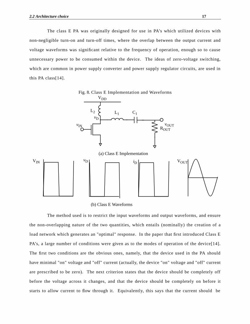
The class E PA was originally designed for use in PA’s which utilized devices with
non-negligible turn-on and turn-off times, where the overlap between the output current and
voltage waveforms was significant relative to the frequency of operation, enough so to cause
unnecessary power to be consumed within the device. The ideas of zero-voltage switching,
which are common in power supply converter and power supply regulator circuits, are used in
this PA class[14].
Fig. 8.Class E Implementation and Waveforms
The method used is to restrict the input waveforms and output waveforms, and ensure
the non-overlapping nature of the two quantities, which entails (nominally) the creation of a
load network which generates an "optimal" response. In the paper that first introduced Class E
PA’s, a large number of conditions were given as to the modes of operation of the device[14].
The first two conditions are the obvious ones, namely, that the device used in the PA should
have minimal "on" voltage and "off" current (actually, the device "on" voltage and "off" current
are prescribed to be zero). The next criterion states that the device should be completely off
before the voltage across it changes, and that the device should be completely on before it
starts to allow current to flow through it. Equivalently, this says that the current should be
L2
ROUT
vOUTvIN
VDD
L1 C1vD
(a) Class E Implementation
vD VOUTVIN
(b) Class E Waveforms
iD

2.2 Architecture choice 18
zero before the voltage across the device increases away from zero, and that the voltage across
the device should return to zero before current is allowed to flow in the device. This allows for
absolutely no power to be lost in the device independent of non-ideal switching times, since the
circuit input and output are controlled such the device output voltage and current will never be
concurrently non-zero. Thus their product, which represents the power lost in the device, is
always zero, making the circuit 100% efficient.
There are several other criterion which need to be satisfied, most notable of which is
the fact that not only should the device output voltage be zero before the current starts to flow
in the device, but also that the time derivative of the voltage at the switching instant be zero as
well. This ensures that if there is a deviation in the switching instant from the ideal switching
time (when the output voltage is zero), the output voltage will be very small, and the power
lost in the device due to this non-ideality will be relatively small [14]. With all these
conditions satisfied, very high efficiencies can be achieved. However, until recently, Class E
PA’s have not really been feasible at PCS RF frequencies (several hundred megahertz and up),
because of the size of the passive components needed in the standard Class-E output
configurations. However, recent publications have indicated slightly different topologies, with
more viable passive component sizes, especially for CMOS (where the large parasitic drain-
bulk capacitance can cause problems in topologies that require small capacitances at the device
output)[15].
There ends a brief discussion of the different classes of Power Amplifiers. More in-
depth information can be found in some of the papers referenced in the previous sections, but
unfortunately, a lot of information resides in the heads of PA designers in industry, and much
of the knowledge used in PA design can be obtained only by talking with experienced designers
and by working with them on PA design.

2.2 Architecture choice 19
2.2.3 Linearization Methods
Several methods of linearizing PA’s do exist, and they are all relatively complex.
Most of these linearization schemes, when implemented, have been implemented at the board
level (that is, with off the shelf components) or in multiple-chip solutions, and have not really
been explored at the integrated single-chip level. Moreover, it is slightly a misnomer to refer
to them as power amplifier linearization schemes, as they really encompass the entire
transmitter, and thus are better referred to astransmitter linearization schemes. They are
decidedly complex, and are mentioned here to flesh out some of the background on Power
Amplifiers (PA’s).
2.2.3.1 Cartesian Feedback
Cartesian Feedback takes the basic concept of negative feedback for linearization and
applies it to the high-frequency PA realm. Applying negative feedback at high frequencies
gives cause for worry, because while it can increase the linearity and the frequency of any
poles that might exist, it will also reduce the forward gain of the amplifier. In the case of a
CMOS PA, the device is being pushed to give as much gain as it possibly can, and thus any
reduction in gain whatsoever is deleterious and undesirable.
Cartesian Feedback, however, avoids that problem by doing the negative feedback at
low frequency. As a result, the RF PA appears as if it is operating in an open-loop manner, and
to first order is not subject to the gain reduction that negative feedback can cause. The
standard block diagram for Cartesian Feedback is shown in Figure 9. As mentioned above, the
linearization works around the entire transmitter, not just the PA, and thus is not direct linear
feedback at the PA’s operating frequency. As shown, the baseband digital bits are put through
a D/A converter, the resulting signals (both I and Q channel) are put into a modulator, which
combines the signals and upconverts them to the RF frequency (the exact method of
conversion, i.e. direct conversion, heterodyne, etc., is not really important). The RF signal is
amplified to the necessary power level from the PA. So far, this is a standard open-loop

2.2 Architecture choice 20
transmitter. At this point, an attenuated version of the RF PA output is demodulated, producing
baseband analog versions of the non-linear PA’s output, which are then subtracted from analog
version of the digital bitstream sent to the PA. This method of linearization linearizes the PA
signal within a smalllinearizing bandwidth bl , which is encompassed by a largeroperating
bandwidth bo. That is, the PA can linearize the signal for any band of sizebl within the fixed
bandbo.
Cartesian feedback amplifiers in literature have been seen to provide as much as 50 dB
of linearization; i.e., the magnitude of undesired spectral components adjacent to the desired
signal, due to intermodulation, spectral regrowth, or other phenomena, has been reduced by 50
dB or more through this technique [16]. Several papers have also reported linearizing
bandwidths on the order of several hundred kHz inside operating bandwidths of tens of MHz
[16]. However, there are limitations to this technique. The linearization is only as good as the
matching of both gain and phase between the upconverting modulator in the forward path and
the downconverting modulator in the feedback path. Moreover, the stability of the loop must
be guaranteed, which sets tight requirements on the loop gain and loop bandwidth [16]. Both
of these affect the amount of linearization provided as well as the available linearizing
bandwidth. Thus very tight control must be exerted over the components in the loop as well as
the overall performance of the loop.
Fig. 9. Cartesian Feedback Architecture
Σ
Σ
IQ Modulationand
Upconversion
Nonlinear RFPA
IQ Modulationand
Upconversion
fLO
I
Q

2.2 Architecture choice 21
2.2.3.2 Predistortion and Adaptive Predistortion
The Predistortion method of linearization is similar to the cartesian feedback method,
in that it looks to modify the signal at the input of the PA, but moves the linearization one step
back in the transmitter chain. The Predistortion method makes use of a DSP by storing known
predistortion coefficients in a lookup table (LUT), which are then used to predistort the input
digital bitstream to create a signal that will generate a linear representation of the desired
input. The coefficients are generated based on the known distortion characteristics of the PA.
Adaptive Predistortion takes this notion one step further in that it periodically senses the PA’s
output in order to update the coefficients in the DSP for any time-varying non-linearities in the
forward path. Because the feedback loop is only closed at selective times, the linearized
transmitter is essentially open-loop and can be viewed as unconditionally stable [17]. This
method can be useful when the system already incorporates a DSP, which may remain unused
or partially unused in this transmit time.
The basic structure of a Predistortion implementation can be seen in Figure 10. It can
be seen that this method is somewhat similar to the Cartesian Feedback method mentioned in
the last section when in its adaptation mode, but that the signal fed back is converted to a
digital representation using an A/D converter and compared to the input bitstream in order to
update its predistortion coefficients. While the linearization is not being adapted, the
transmitter is strictly open-loop, and thus stability is not an issue. The digital I and Q channel
bits are combined in order to generate the value used to index the lookup table; the methods of
combination can include using both the I and Q bits in order to generate an exact 1-to-1
mapping between the digital complex plane and the RF output plane, or possibly combining the
I and Q bits to generate and effective signal magnitude [19]. The latter can give a significantly
smaller LUT.
Practical considerations can set bounds on the amount of linearization attained
through this method. The amount of linearization can be limited by the sampling frequency of
the digital input bits. The linearizing bandwidth should nominally be limited by the sampling

2.2 Architecture choice 22
frequency of the input, due to the Nyquist Sampling criterion. Reduction of the sampling
frequency can cause limited linearization in higher order products, with the linearizing
bandwidth decreasing as the sampling rate is decreased [19]. Moreover, when the feedback
loop is active for coefficient adaptation, extremely tight control must be maintained in order to
ensure correct adaptation. Clearly, since this feedback is periodic and not continuous like in
the Cartesian Feedback (CF) case, the amount of errors in the adaptation loop introduced by
the loop components will be reflected directly in the updated coefficients.
Fig. 10. Digital Predistortion Architecture
Again, these techniques have demonstrated reduction in IM components by more than
50 dB for the systems in which they were implemented [17][19]. However, one other
significant drawback of this technique is that a DSP is needed for this linearization scheme,
which can significantly add to the total power consumption of the transmitter. Remember that
any extra power spent to linearize the PA directly reduced the effective efficiency of the PA;
none of the extra power consumption goes to the load. This reduction in efficiency may or may
not be allowable in a given system or a given implementation, and this must be considered
when implementing the transmit path.
2.2.3.3 Feed Forward
This method does not use feedback; as the name implies, it uses a feed-forward
technique in order to linearize the PA output. The block diagram of the Feed Forward method
fLO
Predistorterikqk
Lookup Table(LUT)
Distortion Estimation
D/AQuadratureModulator
PA
QuadratureDemodulator
A/D
Signal
Magni-tude

2.2 Architecture choice 23
is shown in Figure 11[18]. As shown, the RF input is split into two paths. The first path
contains the nonlinear power amplifier which is to be linearized. The nonlinear amplified
signal is then tapped for an attenuated version of its output and subtracted from a delayed
version of the original RF input. Since the RF input contains only the desired signal, whereas
the attenuated version contains the desired signal as well as other harmonics due to the
nonlinear nature of the PA, the difference contains only the unwanted harmonics, at least in an
ideal sense. This is shown in Figure 11. The difference is then amplified using a linear PA,
which is then subtracted from a delayed version of the PA output. The linear PA ideally does
not add any extra frequency components to its input, and thus when it is subtracted from the
original PA output, it ideally cancels the nonlinearities in the first PA’s output, and thus the
final output is a linear representation of the input.
Fig. 11.Feed Forward Architecture
While the Feed Forward technique is completely open-loop and thus never suffers
from any stability concerns, the matching between the two paths is of critical importance. The
artificial delay added to the lower path to compensate for the delay through the RF PA (as
shown in Figure 11) must closely match the delay introduced by the RF PA; otherwise, the
subtraction will not accurately cancel the linear terms in order to generate the error signal.
Similarly, the delay introduced into the upper path in order to compensate for the delay through
the linear PA used to amplify the error signal must match that delay. Mismatch in that delay
+
PA
TimeDelay
TimeDelay
Error Amplifier(Linear)
+Output
SplitterInput
Nonlinear
- -

2.3 Conclusion 24
can cause poor distortion cancellation, since the combiner will combine two signals that are
effectively out of phase, possibly increasing the phase distortion.
Moreover, efficiency degradations can be problematic in this case, as they were with
Adaptive Predistortion. A linear PA is needed in the error path of the Feed Forward technique.
One of the reasons to use a nonlinear PA in the first place (which thus required the
investigation of linearization techniques) was the better efficiency of the nonlinear PA. The
Feed Forward technique re-introduces a linear PA into the signal path. It must be noted,
however, that using a linear PA to amplify the error signal does not have to consume as much
power as using that same linear PA as the PA used to amplify the RF input. The power level at
the output of the linear PA in the Feed Forward case is only that required to adequately cancel
the error components in the output, which need not require the amount of amplification (and
thus power consumption) of the original input signal. That is, the error signal may only need
to be amplified to a small fraction of the output peak power in order to sufficiently reduce the
error components, and thus the power consumed in the linear PA may be small. That being
said, however, it must be remembered that 100% of that power detracts from the overall
effective efficiency of the PA, and thus the amount of power "wasted" there must be carefully
monitored.
Even with these drawbacks, the Feed Forward technique can be very valuable. The
literature has indicated linearization of up to 60 dB in a high power system [18], which can be
very useful. This technique can be especially significant in a base station-type application, or
one where there is an essentially infinite power supply available.
2.3 Conclusion
The above discussion, while not entirely relevant to the final outcome of this report, is
of crucial importance in the study of PA’s. The different types of PA’s and what methods might
be used to linearize them can be very important in the design process, as meeting the needed

2.3 Conclusion 25
specifications with the minimum power expenditure is a critical concern. It should be
emphasized again that many linearization techniques, including the ones listed above, have
mainly been used at the board level, and not at the single chip level. The freedom from the
restrictions that single-chip (CMOS) integration force upon the designer allow techniques to be
used that might not be considered practical in an integrated environment. While there is some
research going on in an integrated version of at least one of the linearization schemes
mentioned above, there are currently no integrated versions of a linearized transmitter in the
literature.

3.1 Introduction
26
3Design Goals and Approach
3.1 Introduction
The goal of this research was to design and implement an all-CMOS RF Power
Amplifier (PA) that could be integrated into an all-CMOS transmitter and eventually an all-
CMOS transceiver. This is a decidedly large change from the current conventional wisdom
regarding PA’s, as most current PA’s are neither integrated nor CMOS. This requires a slightly
different approach to PA’s, in general, than the standard approaches now, most of which are
implemented in discrete Gallium Arsenide (GaAs) devices.
CMOS faces many disadvantages that are less prevalent in GaAs. In general, theft of
CMOS processes are much lower than those of comparable line width GaAs processes, and as a
result, CMOS is not as well-suited for high-frequency operation than GaAs. Moreover, GaAs
tends to have better gain capability than CMOS due to the better mobility of electrons in GaAs.
In the current design project, both high-frequency operation as well as well as significant
amplification are required and thus CMOS is, in a sense, doubly deficient for this application.

3.2 Design Goals 27
However, as mentioned earlier, CMOS does have its advantages, not the least of which is its
lower cost and its ability to be integrated.
3.2 Design Goals
3.2.1 DECT Specifications
DECT is the Digital European Cordless Telephone standard (it has since become the
Digitally Enhanced Cordless Telephone standard). It is a standard which allocates ten channels
of 1.728 MHz each for communications, and then time-division multiplexes users within a
single channel. In the DECT standard, the key specifications for the Power Amplifier (PA) are
the power output levels and the time-domain transmit masks. The efficiency is a key concern,
but is not specified in any standard; it is an optimizable parameter, dependent on satisfying all
the other requirements put forth by the standard.
Fig. 12. DECT Frequency Allocation
The DECT standards specifies that communications will be done in a frequency band
with a width of 17MHz centered at approximately 1.89GHz, making it a narrowband
communications system. The band consists of 10 channels, each of width 1.728 MHz, but with
a data rate inside the channel of 1.152MHz. Each channel is furthermore divided into 12
different time slots, each of those carrying the communications traffic of a different user. The
basic frequency bands are shown in Figure 12. The power output levels in DECT vary from
approximately 19 dBm, or 80 mW, all the way to 24 dBm, or 250 mW[20].
Cha
nnel
1
Cha
nnel
2
Cha
nnel
10
Slo
t 1
Slo
t 2
Slo
t12
1.880G 1.897G
t
f

3.2 Design Goals 28
The transmitted power time-domain mask is shown in Figure 13[20]. The output
power must ramp up from its essentially zero value while the device is not transmitting to its
final value in a short time. Moreover, once at the transmit frequency, the power should not
deviate from the desired value. Finally, the ramp down is just as critical as the ramp up,
indicated by the amount of time in which the power must return to its off-state minimum value.
Fig. 13. DECT Transmit Power Time-Domain Mask
These are the specifications of the DECT standard that are relevant to the design of the
power amplifier.
3.2.2 Design Goals
As stated before, the overall goal of this project was to design a RF CMOS Power
Amplifier (PA) that could be used in an integrated radio transceiver. This high-level goal in
itself presents a few challenges as well as a few simplifications, even before analyzing the
goals required by the DECT standard. In order for the PA to be easily integrated into a larger
system, it must ideally operate under the same supply voltage. Many of today’s analog IC
applications are being implemented with a power supply of 3.3V or lower for many reasons,
including power consumption (especially in battery operated applications such as this) and
ease of integration with digital blocks. The system that this PA was designed for also was to
operate under a 3V power supply, setting that as one of the goals of this project.
The fact that this PA is meant to be integrated also helps out in one respect, and that is
that it reduces the amount of power needed to drive the PA, which can help raise the efficiency,
27µs
10µs
10µs
10µs
27µs20nW
25µW
20nW
25µW
Desired O/PPower Level
2dB

3.3 Approach 29
especially in a CMOS process, where generating a lot of gain at high frequencies is
challenging. In a discrete PA, the input must be driven from off-chip, and that requires that a
50 Ω load be presented to the previous stage, causing power to be wasted. However, in the case
of an integrated PA, a purely capacitive load can be presented to the previous stage, requiring
significantly less power to drive it. In order to ensure this is the case, though, it is important
that the distances between the previous stage and the input to the PA be much less than the
wavelength at the fundamental frequency, so that the circuit may be treated as a lumped circuit,
and not as a distributed system. At 1.9GHz, the wavelengthλ is approximately 15 cm,
allowing the circuit to be treated as lumped, at least in the on-chip case.
The rest of the goals of this project are set by the DECT standard. The goals are to
achieve a peak power of 250 mW into the load, while meeting the transmit masks specified by
DECT. The output power must also be controllable, to satisfy the output power control
requirements. Finally, a target efficiency of between 30% and 40% was chosen.
3.3 Approach
Because of CMOS’s disadvantages in the amplification and high frequency realms, the
first priority is to find a way to get the desired and necessary gain at the desired frequency.
The specifications of this project call for a differential voltage gain of 10 at 1.9 GHz. Theft of
this process is on the order of 5-10 GHz (depending on the Vgs-Vt of the device), so ideally,
the maximum gain of a single stage device is about 5 at 1.9 GHz. In order to achieve the
required gain, some non-standard methods (at least in terms of power amplifiers) needed to be
used to meet the required goal. They include the choice of process, the need for multiple
stages, the need to provide inter-stage tuning, and differential architecture, and finally, the
choice of PA class. Each of these will be explained in the following sections.

3.3 Approach 30
3.3.1 Process Choice
A strong trend in industry has been the stranglehold that Gallium-Arsenide (GaAs)
processes have had on the Radio Frequency (RF) PA market. GaAs has inherently better high-
frequency performance, and GaAs process have often been built with better contacts and other
process steps that allow PA's to be built more easily. Not only that, but the extremely highft's
of GaAs allow for higher gain (and thus higher amplification) than CMOS for a given
frequency and feature size, make it more attractive than CMOS for the highest-frequency
blocks. The advantage that GaAs has had is so great that the higher cost of building a chip
(and often multiple chips) in GaAs has never really been an issue, even in an era where a low-
cost product is crucial. With good high-frequency performance, a device can amplify well,
requiring very little input drive to obtain a certain output level, which increases both the power
gain and the Power-Added Efficiency (PAE), one of the key PA metrics. Also, the good high-
frequency performance is indicative of low parasitic elements (remember,ft is approximately
gm/Cgs), and this prevents power from being wasted in driving parasitic elements which are
extraneous to the desired goal of driving the output load.
However, with the constant advances in silicon CMOS processing, there has been
thought recently that CMOS devices could compete with GaAs at some of the lower reaches of
the RF wireless communications spectrum. As the channel length of a CMOS device decreases,
the gain it can provide increases, while the parasitics decrease, or equivalently, thefT of the
device increases as the inverse of the channel length squared. Ideally, there should be a point
for which a state-of-the-art CMOS process will be able to compete with a (somewhat) run-of-
the-mill GaAs process. Since silicon CMOS is less expensive and a silicon MOS PA allows for
integration with other transmitter or transceiver blocks (many of which can currently be
implemented in CMOS), such a competitive CMOS process (if it exists) can offer many
advantages over a performance-comparable GaAs process.
The important question, which is really at the heart of this project, is the following:
Will Silicon MOS be able to perform as ideally expected?

3.3 Approach 31
3.3.2 Multi-Stage Design
In an amplifier specification where the necessary gain can not be obtained in one
stage, the logical step is to try a multistage design, allowing the desired gain to be spread over
multiple stages, reducing the gain for each stage to a value that can be achieved in one stage.
However that is not the only concern we have here. Another goal of this project is to design a
power amplifier that can be integrated onto the same chip with a full transmitter as well as
(eventually) with the entire transceiver. As a result, the input to the PA must be one that can be
driven by the output of a mixer or whatever block might precede the PA. In this case, the input
to the PA block presents a totally capacitive input to the previous stage (the gate of a
MOSFET), and thus the size of the first device of the PA must be reasonably sized, although
the required output power in a PA usually necessitates very large output devices. Thus we see
a few important points here: the PA must be multi-stage, it has to have large output devices,
and it has to have reasonably sized input devices so that it presents a small load to the driving
stage. This again points to needing a multi-stage PA, in which the devices increase in size
through the stages.
A key point that must be noted here is that while the first stage should have a
relatively low input capacitance so as not to overly load the previous stage, a significant
victory can be achieved in a CMOS implementation because of the possibility of integration.
In most transmitters today, the PA is implemented on a separate chip from the stage that
precedes it, which necessitates the need for the previous stage to be output matched to 50Ω,
and the PA to be input matched to 50Ω. The previous stage must be able to drive a 50Ω load,
which can require a lot of power to be dissipated. An integrated CMOS PA can present an
entirely capacitive load to the previous stage, as it can be included on the same chip, and so the
input to the PA can be considered a lumped element. The purely capacitive input can definitely
be designed to present a much smaller load than 50Ω, providing what could be a substantial
power savings. Thus while the use of CMOS may require extra stages to compensate for lower

3.3 Approach 32
gain capabilities, a significant power savings may be gained in the removal of the need to drive
a 50Ω load at the input of the PA.
Beyond this, though, the number of stages needs to be determined. It is not readily
apparent what the optimum number is. One must realize, however, that there is some optimum
point, and the best thing is not to have an indiscriminately large number of stages with a
gradual increase in size, and only a minimal gain per stage. The most important restriction on
the PA as a whole is its power consumption and efficiency, and each stage that is added only
increases the power drain on the battery; thus there will be an optimum point at which all the
desired criterion are best met. In this design, the optimum was a three stage amplifier, which
both allows for a relatively low gain per stage (slightly greater than two), a gradual increase in
size from a small first stage device to a large output device, and a reasonable limit on the power
consumption.
3.3.3 Tuned Design
Another method of extracting gain from lowft devices is to somehow tune out the
elements that cause theft to be low; namely, the capacitances associated with the devices. In
the case of an MOS device, the gate capacitance is the dominant capacitance contributing to the
decrease in gain with frequency. One method of tuning the capacitances out is to use inductors
to create a circuit that resonates at the desired frequency, and hence can ideally present an
infinite impedance to the driver. In essence, the region of operation can be “shifted” up in
frequency by creating this tuned element; lower frequency performance will be diminished by
the small load the inductor presents at those frequencies, but the high frequency operation
(hopefully at the frequencies of interest) can be improved. For example, assume a certain gain
stage had the frequency response given in Figure 14(a), with the first pole at a certain
frequencyω0. By using an inductor, the poleω0 can be shifted upward in frequency (at the

3.3 Approach 33
cost of adding a low frequency zero), and the device can be employed at the higher frequencies
that are needed in this application, as shown in Figure 14b.
Fig. 14. Ideal Effect of Tuning on Gain vs. Bandwidth
Equally important, though, is the fact that creating a resonant structure decreases the
amount of current that is needed to drive the large capacitances inherent in large driver stages.
A parallel resonant structure needs only to be supplied with an amount of current that is less
than the circulating current in the resonant structure by the quality factor, orQ. The Q is a
ratio which compares the imaginary parts of the impedance to the real parts of the impedance,
in order to determine how lossy an element is. Thus the higher the Q of an element is, the
lower its resistive component is, and the less power that is lost through dissipation through the
real part of the impedance. For an ideal LC parallel resonant circuit, with infinite Q, no current
needs to be supplied by an external force, as the structure will resonate with any initial
excitation. However, for non-infinite Q’s, the circuit will lose some of the circulating current
due to losses in the resistive components of the circuit. For example, if the inductor is non-
ideal, and has a finite Q due to a parasitic resistance in series with the inductor, the current
circulating will eventually dissipate, and will need to be replenished. Since the amount of
current that needs to replenished is less than the total needed to drive the capacitor, there is a
possible power savings because of the inductor, and a second benefit is derived.
ω0 ω0
Av Av
ω ω
(a) Basic Gain StageFrequency Response
(b) Frequency Responsewith Inductive Tuning

3.3 Approach 34
3.3.4 Differential Topology
The final high-level method used in this approach was the use of a differential
topology, which aided the design of the power amplifier in more than one way. Most power
amplifiers currently available today are designed in a single-ended fashion; after all, most
standard antennas need to be driven with a single-ended signal. However, as analog circuit
design and process technologies progress, the need for lower voltage operation is increasing,
and the large voltage swings needed to generate moderate power levels will not always be
available. With the advent of device feature sizes of 0.6µm and even less, the voltages at
which the transistor or other parasitic junctions break down is reduced as well, and thus
extremely large voltages can not be reliably attained. Hence some circuit design techniques
must be considered that follow the restrictions but yet yield the desired performance.
Fig. 15. Reduction in swing requirements due to Differential Configuration
One way to attempt to solve this problem is to use a differential architecture. The
differential design allows for more dynamic range in the circuit, as the voltage swing
requirements at every node in the circuit are essentially cut in half. For example, if an eight
volt peak-to-peak (pp) swing is required at the output, a single-ended implementation would
need to support the entire eight volts at its output nodevOUT. However, a differential
implementation, in which the output is connected across the two differential output nodes,
would require that each output node only support half of the desired output swing, with the
+ _
(a) single-ended (b) differential
vo
vo
vo
vo+ vo
-vo

3.3 Approach 35
difference between the two providing the required total voltage. This is illustrated in Figure
15.
Another benefit of a differential architecture is the immunity to common-mode (CM)
noise and other disturbances. The final stage of a PA implementation will often be generating
large amounts of AC substrate current, which could cause havoc with a single-ended
implementation, due to fluctuations in substrate voltage, or more generally as large external
noise that could cause the circuit to malfunction. However, in a differential implementation,
that noise, which can be considered to be CM signals, can really be ignored for all intents and
purposes.
3.3.5 Choice of PA Class
Finally, a decision must be made as to which class of PA to design. There are several
factors which go into the class of PA, most of which depend on the communications system for
which the PA is being designed. As stated in Section 3.2, the PA must output a peak of 250
mW, controllable down to a minimum of 0 dBm or 1 mW. It must also be able to meet the time-
domain and frequency-domain transmit masks. In these considerations, the issue of meeting
the transmit masks plays an important role in determining the class of PA to use.
While nonlinear PA’s have great efficiency, their nonlinearity can cause the output
signal to spread (due to intermodulation products, especially if there is a lot of phase noise in
the local oscillator which will cause spreading of the input to the PA), and this spreading of the
output can cause the above restrictions to be violated. Moreover, a key point of the transmit
masks is that during the PA turn-on time (as shown in Figure 13), the transmitted signal must
still meet the spectral mask, which can be difficult for a nonlinear PA. As a result, a nominally
linear class of PA’s was chosen to be used in this design, so as to avoid some of the problems
caused by PA nonlinearity. Since this was really the first attempt at designing and building a
PA, a more cautious route was chosen that would make it easier to meet the spectral mask
requirements. However, maximizing the efficiency was also a concern, and so class AB was

3.3 Approach 36
chosen as the class of PA’s to use in this design. Class AB also translates well into
implementation in a differential architecture, which is another of the approaches that is to be
utilized.
Also, a secondary concern in this choice was the issue of modeling the devices. At the
time that this design process was started, it was unclear how well the existing models for the
process to be used would model a hard-switching, high-frequency nonlinear Power Amplifier.
As such, a linear class AB PA was chosen, in the best interests of some sense of security in the
models.
3.3.6 Chip-On-Board (COB) Die Attachment
Another key decision in this process was the decision to use the Chip-On-Board
(COB) method of die attachment, which facilitated the use of high quality factor (Q) inductors
in this design. In the COB process, the die is attached directly to the Printed Circuit Board
(PCB) through the use of a gold-plated die footprint on the board and a conductive epoxy glue.
Bondwires are connected from the pads on the chip directly to landing zones on the board
(essentially metal traces) which can be brought almost arbitrarily close to the edge of the die
footprint (a minimum distance of a few mils can be required).
By attaching the die directly to the board, several key benefits are obtained. First, the
lengths of the bondwires are minimized compared to those required in a standard package.
With the landing zones so close to the die, the length of the bondwires can be minimized
compared to the lengths of bondwires in packages. This is especially important at RF
frequencies, when the values of lead inductances in many standard packages can present
significant impedances to the circuit. A serious result of these large lead inductance
impedances is that the on-chip electrical ground in a PA can have extreme voltage swings away
from its ideal zero voltage, since PAs source and sink large amounts of current, especially in
the final power stage. Minimizing the lead inductance can reduce the effect of ground bounce,
and can improve the efficiency of the PA.
3.4 Conclusion 37
Also, the use of the COB process allows the length of the bondwires to be controlled
to some extent. The bondwire is a high Q inductor with a value of a few nanoHenries; in the
case that the value of a tuning inductor falls in that range, the bondwire can be used to tune out
the desired capacitance and present a large impedance to the driving transistor. The gain
through each stage of the PA can thus be maximized; the use of low-Q on-chip spiral inductors
may limit the amount of gain through that stage.
Finally, by tying the die footprint to the ground plane on the test board, the footprint
serves as an electrical ground plane for the chip, as well as serving as a mechanism for heat
dissipation. The footprint is electrically connected to a large, electrically quiet ground plane,
aiding in keeping the substrate of the chip as quiet as possible.
3.4 Conclusion
This completes the discussion of some of the design issues that needed to be
addressed, and explains the choices made in the design process, including the decision to use a
Class AB PA in this design. In the next section, the specific circuit-level implementation will
be addressed.

4.1 Introduction
38
4Implementation
4.1 Introduction
Once the architectural decisions have been made, the Power Amplifier must be
realized in a circuit form. The desired output power level must be realized while maintaining
as high an efficiency as possible. Some of the decisions that needed to be made regarding this
design were detailed in the last chapter, and this chapter will detail the circuit level
implementation of the PA.
4.2 Circuit Design
4.2.1 Output Stage
4.2.1.1 Transistor Configuration in the Output Driver Stage
The stage of the PA that actually drives the antenna is often called the power stage, or
the driver stage. This stage needs to be designed first, as the rest of the design, including the

4.2 Circuit Design 39
pre-amplification stages as well as the passive elements, depends on the particulars of this
power stage. Moreover, the specifics of this final stage depend only on already known
quantities.
Fig. 16.Basic Differential Implementation
This stage must, with the available input drive, be able to drive the output load with
the required current, such that the output power is produced. The most basic amplifier that can
be used in this case is a single transistor amplifier, which in this case can be implemented as a
simple common source stage. In Chapter Three, a differential design was proposed, and thus
the most basic differential output stage is shown in Figure 16. This is nominally a simple
differential pair; the only thing missing is the constant tail current. This tail current is not
included because of the large standby power dissipation that would result. In this particular
case, in order to generate 250 mW of output power, as required by the DECT standard, a 100
mA peak sinusoidal current is needed through a 50Ω load. In order to maintain the above
circuit with a tail current, the size of the tail current would have to be that 100 mA, plus
whatever extra current is needed to drive all the capacitances at the output, as well as any
excess current needed to keep the devices saturated throughout the entire cycle of voltage
excursions. This means that independent of the size of the input signal, the amount of current
drained from the supply would be that necessary to drive the maximum output power load, and
thus even for the small output power level situations, the current drain on the battery would be
close to the maximum. Instead, the tail current was eliminated, and the devices were biased
just above threshold, to minimize the DC current taken from the supply. Moreover, this makes
vIN+ vIN
--
Output Load
VDD
vOUT+
vOUT--
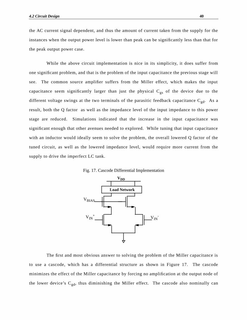
4.2 Circuit Design 40
the AC current signal dependent, and thus the amount of current taken from the supply for the
instances when the output power level is lower than peak can be significantly less than that for
the peak output power case.
While the above circuit implementation is nice in its simplicity, it does suffer from
one significant problem, and that is the problem of the input capacitance the previous stage will
see. The common source amplifier suffers from the Miller effect, which makes the input
capacitance seem significantly larger than just the physical Cgs of the device due to the
different voltage swings at the two terminals of the parasitic feedback capacitance Cgd. As a
result, both the Q factor as well as the impedance level of the input impedance to this power
stage are reduced. Simulations indicated that the increase in the input capacitance was
significant enough that other avenues needed to explored. While tuning that input capacitance
with an inductor would ideally seem to solve the problem, the overall lowered Q factor of the
tuned circuit, as well as the lowered impedance level, would require more current from the
supply to drive the imperfect LC tank.
Fig. 17. Cascode Differential Implementation
The first and most obvious answer to solving the problem of the Miller capacitance is
to use a cascode, which has a differential structure as shown in Figure 17. The cascode
minimizes the effect of the Miller capacitance by forcing no amplification at the output node of
the lower device’s Cgd, thus diminishing the Miller effect. The cascode also nominally can
Load Network
VDD
VBIAS
VIN+ VIN
-

4.2 Circuit Design 41
give better gain from its input to its output because of an increase in the output resistance of
the device.
Another key advantage of the cascode, especially in these high-frequency, high-power
stages is that the cascode provides nice reverse isolation between its output and its input. If
there were to be any significant amounts of feedback between the input and output of the
feedback stage, it would be quite possible for the power stage to go unstable. A common
metric in the stability of high-power PA’s is the stability factork, which is defined as
(Eq 6)
for absolute stability[4], where
. (Eq 7)
In conventional microwave designs, a discrete device, often a GaAs MESFET device,
is thoroughly characterized to determine its large-signal S parameters, which can then be used
in determining the PA’s stability using Eq. 6. However, in the realm of integrated CMOS PA
design, such luxuries are not available to the designer; as such, a different method to guarantee
stability must be examined.
In a standard, single MOS device amplification stage, the output signal can be fed
back to the input by the gate-to-drain capacitanceCgd. At high frequencies, the impedance of
this capacitance decreases, and more and more of the output will be fed back to the input. The
cascode, on the other hand, has no such connection, and thus provides larger amounts of
reverse isolation. Really, the only method of feedback to the input to the final stage is through
parasitic interconnect capacitance, which can be minimized through good layout practices,
reducing the possibility of instability due to feedback by keeping the amplifier an open-loop
system. The stability of the amplifier can and will be verified in SPICE simulations before
sending it for fabrication.
k1 S11
2– S22
2D
2+–
2S12S21----------------------------------------------------------- 1>=
D S11S22 S12S21–=

4.2 Circuit Design 42
The cascode is not without its drawbacks, however. In general, in order to have high
power at the output, high voltage swings, high current swings, or both are required. The
amount of voltage swing or current swing is determined by the output power and the optimum
resistance. For a sinusoidal output,
(Eq 8)
or
(Eq 9)
Ideally, the load resistanceRopt seen by the stage should be as close to the actual value of the
component at the output (in this case, the antenna) as possible, in order to minimize the losses
due to the necessary impedance transformation between the load and the device. The stacking
of devices in a cascode limits the output voltage swing that is available, especially if the goal is
to keep the devices in the saturation region (for MOS devices). If the output voltage swing is
limited, then the current swing must be increased (and the optimum resistance decreased) in
order to achieve the same power. Not only does the reduction in the optimum resistance
decrease the efficiency, due to the now-required impedance transformation at the output, but
the increased current requirement increases the amount of capacitance seen at the output. The
larger capacitance at the output requires more current to drive it, requiring a larger device to
generate the current. As a result, if the voltage swing at the output is limited, it can decrease
the efficiency, as it requires more current to be drawn from the supply to drive this larger
capacitance; this current is not directly driving the load, and directly reduces the efficiency.
Thus the cascode can cause complications in the design of the output.
4.2.1.2 Optimum Load Resistance Determination
The next key step in the design of the output stage is the determination of the load
resistance, which is dependent on the available voltage swing at the output. In an RF or
microwave system, the terminal impedances are all normally designed to be 50Ω by
convention. The purpose of the PA is to drive the antenna, which is nominally modeled as a 50
PV peak
2
2Ropt---------------=
PI peak
2Ropt
2-------------------------=

4.2 Circuit Design 43
Ω resistor. However, there is no guarantee that there will be enough voltage swing available to
drive the antenna with the desired output power. For example, if the available voltage swing is
3V peak and the load resistance is 50Ω, then the power delivered to the load at the RF
frequency will be given by applying Eq. 8
, (Eq 10)
which is not the 250 mW desired in this application.
This then requires that some conversion must take place between the PA output and
the antenna so that the desired power level can be obtained at the antenna. A common and
simple way of doing this is to use an impedance transformation to transform the impedance of
the antenna to a value consistent with the available voltage swing and desired output power.
This transformation network is usually a network of passive, (ideally) lossless components,
usually capacitors and inductors. The transformation network, being lossless, will deliver the
same amount of power to the antenna as the PA delivered to it. In the case where there is a
limited voltage swing and the desired peak power cannot be achieved with the real load, the
optimum resistance will be reduced below that value. In this case, effectively, voltage has been
traded for current, and the required power is achievable, even with the voltage limitations.
In the original design specification, the goal of this research was to design the PA so
that it would operate under a 3V supply voltage. In this design, the output of each stage is
biased at the power supply voltage by an inductor. For a power supply voltage of 3V, which
was one of the design goals, the voltage swing was limited to between 1.8V and 2V peak, in
order to keep the bottom device in the saturation region. According to Eq. 8, the optimum load
impedance is
. (Eq 11)
However, in order to keep the design simple, it was desired to try to keep the optimum
resistance as close to 50Ω as possible. In order to accomplish this, the power supply for the
PV pk( )2
2R----------------- 9
100--------- 90mW= = =
R2V pk( )2
2P pk--------------------- 32Ω= =

4.2 Circuit Design 44
final stage was raised to 5V, giving ample headroom to allow the output node of each side of
the differential configuration to drive 250 mW or more into the 50Ω load.
4.2.1.3 Device sizing requirements
Now that the transistor configuration has been decided, the output stage has to meet
the required peak output power level. Using Eq. 9, the peak current swing needed for 250 mW
of output power is
, (Eq 12)
at the fundamental frequency (equivalent to 5V peak sinusoidal voltage). In order to obtain
this current, the output devices must be large enough to sink that peak current, as well as any
bias current and the current needed to drive the other passive components for the given input
signal at the RF fundamental frequency. The amount of current needed to drive the other
components is highly dependent on the output voltage swing (which is nominally fixed), the Q
factor of the passive network (again, fixed).
In this case, a 100 mA sinusoidal current must be supported through the load. A key
point to note when sizing the devices is that the peak current for a given voltage is different in
the DC and AC cases. The device must be sized so that it can provide the required current
under the AC condition; thus when characterizing the device, the peak current for a given
voltage at the input must be evaluated at the frequency of interest, or in this case, 1.9 GHz. For
this application, the final sizes of the 4 devices in the output stage was 3000µm by 0.6µm.
4.2.1.4 Structure of Passive Components in the Output Stage
Once the transistor configuration has been decided, the structure of the passive
components that make up the rest of the final stage must be designed. The purpose of the
passive components at the output is twofold: first, the imaginary part of the output impedance
at the desired output frequency must be canceled. This is done to ensure that a solely resistive
load is seen and all the output signal at the fundamental frequency is converted into real power;
I pk2P
RLoad--------------- 100mA= =

4.2 Circuit Design 45
imaginary power at the output is wasted. Second, the passive components must, if necessary,
transform the resistance of the load into the optimum resistance for this particular Power
Amplifier (PA) application.
In order to maximize the voltage swing at the output, the drain must be biased at a
high DC voltage. Standard practice in RF PA’s is to bias the output node of the transistor (or
the cascode, in this case) at the power supply VDD through an inductor, often an RF Choke for
AC isolation at the frequencies of interest.
The cancellation of the imaginary portion of the transistor’s output impedance can be
done very simply. The imaginary portion of that impedance usually derives from the output
capacitance of the transistor and any other stray capacitances, possibly due to output
interconnect. The simplest way to cancel that imaginary capacitance is to use an inductor to
create a resonance at the fundamental frequency of operation, which was the method used here.
However, this method does not account for the nonlinearity in the device output capacitance,
which results from the voltage-dependent drain-bulk junction capacitance of the output node.
As the output voltage changes, the output capacitance changes as well, and as a result, the
imaginary part of the total impedance (including the inductor used to resonate the capacitance)
will vary from the ideal. This can give a large capacitive range to match; one solution is to
match the inductance to the average value of the capacitance across the output cycle, which is
what was done here. This minimizes the deviation from the resonance of the tuned circuit as
the capacitance traverses its range of values.
The output stage, including both the RF Choke as well as the impedance matching
inductance, is shown in Figure 18(a), and the equivalent AC circuit is shown in Figure 18(b).
The RF Choke is an off-chip, large inductance that acts as a DC short circuit and an effective
AC open circuit at the RF frequency relative to the other impedances in the circuit. As stated

4.2 Circuit Design 46
in Chapter 3, the impedance matching inductors are implemented using bond wire inductances,
to take advantage of the high Q properties of bond wires.
Fig. 18. Final Output Stage Configuration
4.2.1.5 Biasing
Another important issue in the design is the issue of biasing. This final stage will be
biased just above threshold, as the choice of the Class AB topology mandates. However, as
described in the next section, the previous stage will be inductively loaded, and thus the two
stages can not be seamlessly connected; the two stages must be AC coupled. This is most
easily done through a coupling capacitor. However, the capacitor must be large enough that
there is no significant loss of signal across the coupling capacitor due to the voltage division
between the coupling capacitor and the gate capacitance of the final stage. Moreover, the
parasitic bottom plate capacitance of the coupling cap will increase the effective gate
capacitance of the final stage, causing more signal loss across the AC coupling capacitance. In
order to achieve a balance between signal loss and chip area (as the capacitor size increases, so
does the area required to implement it), a coupling cap value of 20 pF was used.
The actual DC biasing of the stages was done through an off-chip bias; as this design
was a first attempt at design an integrated PA, this allowed the bias voltage of each stage to be
50Ω (modelof antenna)
Off-Chip
VDD
+
_Vin
VDD VDD

4.2 Circuit Design 47
controlled in order to choose the optimum point (in case the bias points chosen in the design
process were not optimum). In essence, it allowed for some more degrees of freedom in
optimizing the design at the testing stage, and would return more information in order to better
tune the design loop.
4.2.2 Pre-amplification stages
Now that the output stage has been determined, the previous stages can be designed in
order to provide the correct amount of gain. The input to the entire PA block has been
specified as being a 0.5V peak (1V P-P) differential signal; that must be gained up to a 10V P-
P signal across the 50W output load. Clearly, the previous block, be it the upconversion mixer
or some transmit filter, will not be able to drive the power stage of the PA. The input of the PA
must present an impedance level that can easily be driven by the previous stage, mandating a
small-sized input device (or pair of devices, in the case of a differential implementation, as in
the present case). At the same time, each of the previous stages must consume minimal power,
as all of that power is “wasted,” at least from an efficiency standpoint, since none of this power
will in any way go towards directly driving the load.
As stated earlier, the PA was designed with 3 stages, with the final stage being the
power stage discussed in the previous section. The second stage was designed to drive the
input of the power stage with an approximately 4V p-p signal in the peak output power case.
As the desired output power decreases, that signal will decrease in value. The impedance
looking into the gate of the input transistor of the power stage is so small, however, that a
tuned network is required to increase the impedance at that node, as discussed in the previous
chapter. The devices in this stage were sized to consume the minimum amount of power and
still provide the necessary current in order to drive the power stage. Again, this necessary
current is dependent on theQ of the inductor used, and since bond wire inductors, with high
Q’s were used, the previous stage was sized to be 400µm by 0.6µm, and would drive the tank

4.2 Circuit Design 48
circuit with a 40mA. The second stage, as well as its output tuning network and the input to
the final stage, is shown in Figure 19.
Fig. 19. Second Stage of PA
Finally, a similar approach was used to design the first stage of the PA, and this gave
the size of the first stage to be 60µm by 0.6µm. The first stage design is shown in Figure 20.
Fig. 20. First stage of PA
The first stage is also used for another key function, and that is for controlling the output
power level. As stated in Chapter 3, the output power level needs to be controlled over a wide
range. In order to accomplish this power control, the first stage is designed to be a Class A
stage. It is simply a differential pair fed by a tail current source, which has a controllable
To3rdStage
To3rdStage
VDD
VDD VDD
vin
To2ndStage
To2ndStage
VDD
StageVDDVDD
vin

4.3 PA Layout 49
value in order to control the gain through the first stage. As the current is increased, so is the
gain in the first stage and equivalently the gain through the PA, modulating the amount of
power delivered to the antenna. This is a relatively simple scheme for power control, which
can easily be implemented by a current DAC, allowing digital control of the output power. For
this implementation, however, the current source used was implemented off-chip, in order to
allow a wide range of available currents to be supplied to the input differential pair. In the case
that the actual chip operation differs from the simulation results, the tail current of the first
stage could be varied over a large range in order to optimize the performance of the PA.
Simulation results of the PA will be presented after the discussion of the layout, as the extra
parasitic capacitances that the layout introduces into the PA affected the values of the inductors
used in the design.
4.3 PA Layout
While the circuit design process of this design was a trying process of many attempts,
once successful, it by no means signaled the end of the design process. The next important
step in the process was the layout of the PA. Not only does the layout add considerable
capacitance to each node, especially the sensitive nodes in the signal path, care must be taken
to minimize resistive losses across metal lines, and to ensure that other losses in the circuit do
not diminish the overall performance that the circuit previously designed had achieved.
4.3.1 Device Layout
The first important point to realize is that the transistors must be drawn in such a
fashion that the RC time constant of the physical gate does not adversely impact the signal
drive. While the devices used in this design are large, especially the output devices, they
cannot just be laid out as one physically long transistor. The input signal has a frequency near
1.9 GHz, and so if the physical resistance of the poly-silicon gate in series with the gate
capacitance of the device has a very slow time constant, the signal driving the transistor itself

4.3 PA Layout 50
will be corrupted. The simplest method of solving this problem is to use a comb structure,
where the large overall width of a device is implemented as a number of transistors in parallel.
While it is true that implementing a transistor with a large width should be
implemented as a number of smaller devices in parallel, this introduces another problem,
especially for a circuit with a large AC signal. The bulk connection of the device will be
carrying a lot of current, due in large part to the AC signal swing at the drain of the transistor.
The reverse-biased drain-bulk junction is a nonlinear capacitor, and so a large number of
substrate contacts are required in order to collect this current. Moreover, these contacts should
not be too far apart, as the bulk current has to flow through the resistive substrate before
reaching the contact; that distance should be minimized as much as possible. If that resistance
is too large, the effective Q of the capacitor (the ratio of its imaginary impedance to its real
impedance) becomes smaller and smaller, and this limits the overall Q of the parallel LC
network. It is well known that the overall Q of a parallel LC network is the parallel
combination of the Q’s; i.e., for an inductor with quality factor QL in parallel with a capacitor
with quality factor QC, the overall quality factor Qeff is given by
. (Eq 13)
This becomes exceedingly important as the device size grows, as the Q of the capacitor will
dominate the overall Q of the network; using bond wires to raise the Q of the inductors is
pointless if the capacitor Q is allowed to become inordinately small. For smaller devices, such
as those in the first two stages of this design, this is less of a concern, as the entire device can
be laid out in a small area, which inherently limits the distance to the substrate contact.
However, for the final stage, the final devices are large enough that even if the device is
parallelized in order to reduce the gate RC time constant, as indicated earlier, the device must
be broken up even further so that substrate contacts can be interspersed in between sub-blocks
of the overall transistor.
Qeff QC QL||QCQL
QC QL+---------------------= =

4.3 PA Layout 51
Practically, the maximum width of a single finger of the fingered (or comb) MOS
device structure was limited to about 20µ/0.6µ in this process, in order to keep the device a
good distance away from the point where the gate RC time constant was a problem. This safe
distance was calculated to be at least an order of magnitude less than the period of interest of
the signals, or less than approximately 50 ps. Also, the large final stage devices, which were
earlier calculated to be 3000µ/0.6µ in size, were split into four separate banks of devices, with
each bank surrounded by a sea of substrate contacts to capture all the AC substrate current.
The layout of the output stage can be seen in Figure 21.
Fig. 21. Layout of Output Stage Devices
4.3.2 Capacitor Layout
In an ideal process, a capacitor is simply a capacitor and nothing more. However, in a
real process, the capacitor is not simply a capacitor; it is also some series resistance. When the
capacitor is made up of two metal layers, this resistance is the resistance of the metal, which is
usually somewhat small, and special layout techniques may not necessarily be needed.
However, for the case of a capacitor made up of two layers of polysilicon, the resistance of the
polysilicon layer is not negligible. This is even more true when the lower layer of polysilicon
is not silicided in those regions where it is under the first region, which is also possible.
PolyGate
Active

4.3 PA Layout 52
Therefore, when considering the layout of the poly-poly capacitor, the series resistance of the
polysilicon layers must be accounted for. If the capacitor is just a bypass capacitor, the series
resistance my not matter, but if the capacitor is in the signal path of the circuit, the series
resistance is very important, and if ignored, can significantly limit the performance of the
circuit.
In the circuit described in this work, two sets of AC coupling capacitors were needed,
in order to set the bias of the inputs of the second and third stages independent of the outputs
of the stages immediately that preceded them. In the case of a multi-chip implementation,
high-Q off-chip capacitors would be used for this purpose; that is not an option in this case, so
on-chip capacitors must be utilized. In order to implement the large capacitors needed to AC-
couple the stages without causing significant losses due to the voltage divider caused by
placing the coupling capacitor in series with the capacitive gate input of the following stage,
poly-poly capacitors were used to minimize the area needed for these capacitors. These
capacitors must be intelligently laid out to reduce their series resistance, which appears
directly in series with the impedance that the gate of the following stage provides. This
reduction can be simply achieved by placing a large number of small capacitors in parallel,
with the overall capacitance being the desired coupling capacitor. This reduces the series
resistance of the poly-poly capacitor by a factor equal to the number of parallel capacitors
used, and this resistance can essentially be made arbitrarily small.
Unfortunately, as will be discussed later in more detail, that was not done in this work,
making testing somewhat difficult. However, this is a key point to note which is not often
readily apparent, at least to novice circuit designers.
4.3.3 Other Layout Issues and Solutions
There are a few other interesting points about this layout that should be noted before
progressing to a discussion of the board design, which will be discussed presently.

4.3 PA Layout 53
First, it should be noted that the bond pads for both the input and the outputs of the
first stage were significantly recessed from the edge of the chip. This was done for a couple
reasons. Most importantly, this allowed larger values of bond-wire inductance to be achieved,
since the length of the bondwire was increased by the distance the pads were recessed. Since
this design was implemented using only bond wires, it was sometimes necessary to use an
inductance value that was somewhat larger than the standard bondwire inductance generated
when using the chip-on-board (COB) method of attaching the die to the board. Secondly,
bringing the pads as close to the actual on-chip circuitry as possible minimizes the extra series
resistance that metal paths on the chip introduce. This extra series resistance goes directly to
reducing the Q of the bondwire inductors, as it adds series resistance without adding an
inductance of consequence.
Another point to note about the layout is that the chip is flooded with substrate
contacts in areas with little or no active circuitry. This point seems to be one that is still not
understood all that well; that is, what is the best method of minimizing the effect of the
modulation of the bulk voltage changing due to AC current flow? One possibility is to put
contacts everywhere possible, but by doing that a potential problem may be introduced;
namely, substrate noise from distant portions of the chip can be introduced into local regions.
However, the benefit to essentially covering the entire substrate with contacts is that the
substrate is turned into an effective ground plane, which can minimize the magnitude of the
substrate noise. The other possibility is to create nominally independent, local substrate
contacts, such that noise from other, more distant parts of the circuit do not leak back into the
local circuitry, but the amount of substrate bounce in certain regions might be larger as well.
Another key point to note is that in many submicron processes today, there exists a low-
resistivity epi-layer underneath the substrate, which can provide low resistance paths for
substrate current and substrate noise to travel to distant portions of the chip. This being the
case, it may not be possible to isolate the substrate in different regions of the chip. In this
circuit, the substrate was covered with substrate contacts as much as was possible, although the
second method may be preferable in other designs.
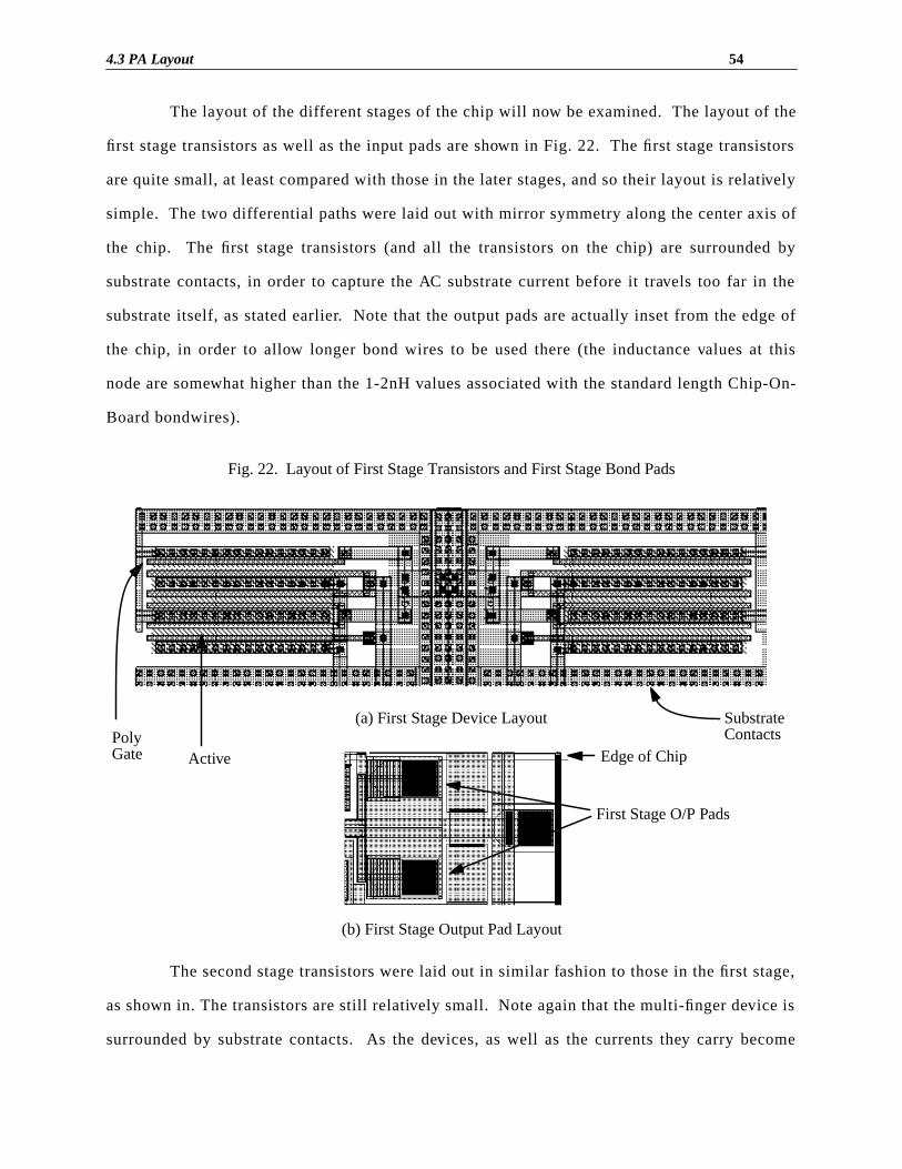
4.3 PA Layout 54
The layout of the different stages of the chip will now be examined. The layout of the
first stage transistors as well as the input pads are shown in Fig. 22. The first stage transistors
are quite small, at least compared with those in the later stages, and so their layout is relatively
simple. The two differential paths were laid out with mirror symmetry along the center axis of
the chip. The first stage transistors (and all the transistors on the chip) are surrounded by
substrate contacts, in order to capture the AC substrate current before it travels too far in the
substrate itself, as stated earlier. Note that the output pads are actually inset from the edge of
the chip, in order to allow longer bond wires to be used there (the inductance values at this
node are somewhat higher than the 1-2nH values associated with the standard length Chip-On-
Board bondwires).
Fig. 22. Layout of First Stage Transistors and First Stage Bond Pads
The second stage transistors were laid out in similar fashion to those in the first stage,
as shown in. The transistors are still relatively small. Note again that the multi-finger device is
surrounded by substrate contacts. As the devices, as well as the currents they carry become
(a) First Stage Device Layout
(b) First Stage Output Pad Layout
Edge of Chip
First Stage O/P Pads
PolyGate Active
SubstrateContacts

4.3 PA Layout 55
larger, the amount of substrate current grows as well, requiring more and more contacts to help
keep the substrate quiet.
Fig. 23. Second Stage Device Layout
4.3.4 Final Circuit
Once the layout has been extracted, the final values of the inductors needed for tuning
purposes can be determined. The final circuit, along with all coupling capacitor values and
inductor values as well as the DC bias at each node, is shown in Figure 24. Though this is a
differential design, only one half of the full circuit is shown, in order to simplify the diagram.

4.4 Simulation Results 56
All the inductor values as well as the final device sizes are listed in the diagram. The final
layout is shown in Figure 25.
Fig. 24. Final Circuit Schematic
4.4 Simulation Results
The simulations of this chip were done using the HSPICE circuit simulator, using
Meta-Software’s (now Avanti) proprietary Level 28 models of the TSMC 0.6mm devices. The
fully extracted circuit, including all parasitic capacitances that were introduced as a result of
the layout, was fully simulated to test the performance. The major simulations run were those
involving an input tone at the desired frequency, with the level of the tail current source being
varied in order to vary the output power level out of the PA.
The PA was to be driven by 1V peak-to-peak differential signal, which needed to be
gained up to 250mW of output power. Figure 26(a) shows the output of the first stage of the
PA, under varying tail current source values. The differential output voltage of the first stage
3.9nH 4pF
1.1nH 20pF
2.3nH
To RFBalun
3V
3V
5V
60µ/0.6µ
400µ/0.6µ
400µ/0.6µ
3000µ/0.6µ
3000µ/0.6µ
RFChoke60µ/0.6µ
2.6V
2.2V
3V
0.8V
0.8V
1.9V

4.4 Simulation Results 57
Fig. 25. Final Full Circuit Layout
OutputStage
SecondStage
FirstStage
Poly-Poly ACCouplingCaps

4.4 Simulation Results 58
can vary from 0.75V to 3V in magnitude, which will cause the output power level to vary as
well.
The corresponding voltages at the output of the second stage are shown in Figure
26(b). Note that it is not particularly instructive to compare the output of the second stage with
that of the first stage and consider the ratio to be the gain of the second stage. Since the second
stage is biased in a Class AB fashion, it does not see the full input that is applied to it. As a
result, the real voltage gain through the devices is actually greater than what it appears to be
from the figures.
Fig. 26. Simulated Output of First, Second, and Output Stages Under Different Tail Current Source Values
Sta
ge 1
Out
put,
VS
tage
2 O
utpu
t, V
Fin
al O
utpu
t, V

4.4 Simulation Results 59
The output of the PA (into the 50Ω load) is shown in Figure 26(c). The output power
delivered to the load is given by
. (Eq 14)
So as the output voltage level varies, the power level varies. The relationship between the
output power delivered to the load and the corresponding first stage tail current is shown in
Figure 27.
Fig. 27. Output Power vs. First Stage Tail Current
Finally, since the output matching network is designed for the peak output power
level, to maximize the efficiency at that point, the efficiency of the PA will vary with the output
POUT
V pk2
2 50Ω⋅------------------ 0.01 V pk
2⋅= =
Pow
er, m
W
First Stage Tail Current, mA

4.5 Conclusion 60
power level. The peak efficiency of the PA is slightly greater than 30% in simulation, but it
drops with the output power level. The efficiency calculated for this PA is the drain efficiency,
which does not include the power needed to drive the PA in the calculation of its efficiency (as
described in Chapter 2). However, because this PA is meant to be used in an integrated
transmitter, it presents only a capacitive load to the block that is driving it. As a result, the
amount of power necessary to drive the PA once it is included in the overall transmitter will be
very small, and thus it was not included in the efficiency calculation. A graph of simulated
efficiency versus output power level is shown in Figure 28. At the peak output power level, the
efficiency is 31.1%. At lower levels, the efficiency drops off, which is to be expected; as the
desired output level decreases, the amount of current needed to generate the output power for a
given load resistance does not decrease linearly with power.
4.5 Conclusion
In this section, the design and layout of a 250 mW PA (peak power is actually
300mW) is described. The design of the output matching network as well as the design of the
individual stages was discussed. The layout process was also explained in great detail.
Finally, simulation results for this power amplifier were discussed as well, with a peak
efficiency of 31.1% obtained for the peak output power level of 300 mW.

4.5 Conclusion 61
Fig. 28. Drain Efficiency vs. Output Power Level
Effi
cien
cy, %
Output Power, mW

5.1 Overview
62
5PC Board Design and Chip
Testing
5.1 Overview
In any design of an RF IC block, it quickly becomes apparent that the design process
does not end when the circuit is down on paper, nor is it finished when the layout is finished;
the board design processes is also critical to the working of the overall block. Not only is the
board the interface between the chip and the test equipment, it also can impact the performance
of the chip; as such, it must be carefully designed. In this section, the process of the board
layout and design is discussed, and those issues that were critical to the design will be
highlighted. Then the testing process and the results of that process will be detailed.
5.2 PC Board Design
As mentioned earlier in this report, the die was to be attached to the board using the
Chip-On-Board (COB) method, in which the die itself is glued to the board using a conductive
epoxy glue. The key benefit of this method of die attachment is that it minimizes the amount of

5.2 PC Board Design 63
bond-wire inductance that individual bond-wires add to the circuit. It also brings the value of
the bondwire inductance more in range with what is needed by the circuit, making bondwires
usable as high Q-factor inductors to be used in the tuning circuitry.
The board needs to include the power supply voltage sources, as well as the bias
voltages needed to drive the current source. Moreover, the board needs to include the bypass
capacitors for those sources. It also needs to include the matching networks and the RF baluns
needed to convert the signal from single-ended to differential (at the input) and back again (at
the output). The first step in designing the board is to place the footprint for the die, which is
just a large square of gold to which the die will be glued. This footprint is filled with vias
which are tied to the ground plane of the board. Thus it serves as a large ground plane which is
tied directly to the substrate of the die, which not only helps to keep the substrate voltage
quiet, but also helps with the heat dissipation. In order to minimize the length of the ground
bond wires, the ground bond wires can be bonded directly to this die footprint, instead of
creating separate landing zones for each ground pad.
Each of the on-chip DC bias points (e.g., at the inputs of the second and third stages)
was created using an off-chip current source which feeds into a diode connected MOS device
on chip, creating a bias voltage that could be changed for test purposes. Similarly, the tail
current source of the chip was created using an on chip current mirror fed by the off-chip
current source. The differential RF signal traces, which exist on the board between the baluns
and the chip were laid out to have a 25Ω characteristic impedance in order to match the
terminal impedances; the single-ended lines were laid out to have a 50Ω characteristic
impedance for the same reason.
The final board components are shown in Figure 29. The RF Choke was actually
implemented as a 18nH surface mount inductor, which actually had a large impedance at the

5.3 Chip Testing 64
operating frequency of 1.89GHz. The balun used in this design was a MuRata 1.9GHz 1:1
transformer, which had close to 3dB of insertion loss.
Fig. 29. Components on RF Board
5.3 Chip Testing
The final step in this design was to actually test the chip. This did not meet with the
success desired; this final portion of the process revealed a key layout error that essentially
prevented the chip from being tested at all.
The first step in the testing was to use an HP Network Analyzer in order to obtain the
S-Parameters for the design. Using the Network Analyzer, a signal of between 0 and 10 dBm
was input to the chip, so that the key S-parameter could be obtained. However, while it seemed
that reasonable S11 and S22 parameters were obtained, the S21 (a measure of the gain from
input to output) was very small; so small, in fact, that it was clear that there was no gain
through the chip. The reason for this was determined after reviewing the layout.
Unfortunately, the layout of the interstage AC coupling capacitors was done without
accounting for the series resistance of the polysilicon. Especially for the AC coupling
capacitor between stages two and three, the series resistance of the polysilicon is comparable
to the input impedance of the second stage, if not larger. Thus most of the signal is lost across
Input fromNetworkAnalyzer
RFBalun
DeviceUnderTest
3V
5V
First StageBondwireInductors
Second StageBondwireInductors
RFChoke
RFBalun
Output ToNetworkAnalyzer

5.4 Conclusion 65
the AC coupling capacitor, and very little signal reaches the input of the third stage. As a
result, the chip produced very little output power, and thus could not effectively be tested to
obtain results as to the quality of the design.
5.4 Conclusion
This chapter detailed the design of the test board used in the chip verification process
as well as the testing process, which unfortunately had to be curtailed due to layout problems.
The board designed included all the voltage sources and bias current sources, as well as the
matching networks and RF baluns used to convert the signal from single-ended to differential
and back.

6 Conclusion
66
6Conclusion
This work attempted to design and build a prototype RF Power Amplifier that could be
used in a system built to meet the DECT standard. A host of classes of RF Power Amplifiers
was reviewed, as well as methods that could have been used to linearize the nonlinear classes
of Power Amplifiers. A Class AB CMOS Power Amplifier was designed in a 0.6µm CMOS
process that delivered greater than 250mW of peak output power with 31.1% efficiency in
simulation.
The PA was implemented in a differential configuration, so as to minimize the amount
of substrate current injected at the signal frequency, as well as to improve the dynamic range at
the output and to increase the common-mode rejection of the circuit. The PA was designed in a
CMOS process to allow it to be integrated on a single-chip with a full transmitter. The design
used 3 stages to generate the power necessary; a Class A first stage, which controlled the
output power level, followed by two Class AB stages to generate the final power level. The two
Class AB stages used cascoded stages, both to reduce the Miller effect on the MOS gate-drain
capacitance as well as to limit the voltage seen across the MOS oxide. Bondwire inductors
were used as high-Q alternatives to on-chip spiral inductors, which is especially useful in
minimizing the resistive loss in the inductors in the power stage.

6 Conclusion 67
A test board was also designed, which included all the necessary DC supplies as well
as the RF matching components and the baluns necessary for the single-ended to differential
conversion. Once the testing process was under way, a layout error was discovered. The AC
coupling capacitors used between stages were poorly laid out, as these capacitors were not laid
out to minimize the polysilicon series resistance. As a result, the testing process was unable to
verify the actual working of the design.
However, the design process was valuable, in that much was learned about PA’s in
general as well as the method of designing a PA. While the results obtained in simulations
were not verified, it is this author’s opinion that a version of this chip with the layout of the AC
coupling capacitors corrected would have verified the simulation results. Because of the
difficulty of obtaining another run in the TSMC process, a second revision of this chip was not
attempted, but, as stated, the process of designing the chip from start to finish was invaluable.

References
68
References
[1] P. R. Gray and R.G. Meyer, “Future Directions of Silicon IC’s for RF PersonalCommunications,” Conference Proceedings, 1995 Custom Integrated CircuitsConference, May 1995, pp. 93-90.
[2] J. C. Rudell, et. al., “A 1.9GHz Wide-Band IF Double Conversion CMOS IntegratedReceiver for Cordless Telephone Applications,”Conference Digest, 1997International Solid-State Circuits Conference, Feb. 1997, pp. 304-5.
[3] P.R. Gray and R.G. Meyer,Analysis and Design of Analog Integrated Circuits, ThirdEdition, John Wiley & Sons, New York, 1993.
[4] G. D. Vendelin, A.M. Pavio, and U.L. Rohde,Microwave Circuit Design Using Linear andNonlinear Techniques, John Wiley and Sons, New York, 1990.
[5] M. Rofougaran, “A 900 MHz CMOS Power Amplifier for a Wireless Transceiver,” MastersReport, University of California at Los Angeles,1995.
[6] J. Griffiths and V. Sadhir, “A Low Cost 3.6V Single-Supply GaAs Power Amplifier For The1.9-GHz DECT System,”Conference Proceedings, IEEE NTC ‘95 The MicrowaveSystems Conference, Orlando, May 17-19, 1995, pp. 37-40.
[7] M. Maeda, et. al., “A High Power and High Efficiency Amplifier With Controlled Second-Harmonic Source Impedance,” Conference Proceedings, 1995 IEEE MTT-S, 1995, pp.579-82.
[8] S. Makioka, et. al., “A High Efficiency GaAs MCM Power Amplifier for 1.9GHz DigitalCordless Telephones,”Conference Proceedings, IEEE 1994 Microwave andMillimeter-Wave Monolithic Circuits Symposium, 1994, pp. 51-4.
[9] M. Nagaoka, et. al., “High Efficiency Monolithic GaAs Power Mesfet Amplifier Operatingwith a Single Low Voltage Supply for 1.9 GHz Digital Mobile CommunicationApplications,” Conference Digest, 1994 IEEE MTT-S, 1994, pp. 577-80.
[10] E. Camargo and R.M. Steinberg, “A Compact High Power Amplifier For Handy Phones,”Conference Digest, 1994 IEEE MTT-S, 1994, pp. 565-8.

References 69
[11] S-J. Maeng, et. al., “A GaAs Power Amplifier for 3.3V CDMA/AMPS Dual-Mode CellularPhones,” IEEE Transactions on Microwave Theory and Techniques, Vol. 43,December 1995, pp. 2839-43.
[12] F. Ali, et. al., “A Study of Class C Operation of GaAs Power HBTs,”Conference Digest,1995 IEEE MTT-S, pp. 721-4.
[13] A. Asensio and F. Perez, “Design and Optimization of High-Power Pulsed Class-CMicrowave Amplifiers,”, Conference Proceedings, IEEE Symposium on Circuits andSystems, New York, 1991, pp. 2371-4.
[14] N. Sokal and A. Sokal, “Class E-A New Class of High-Efficiency Tuned Single-EndedSwitching Power Amplifiers,”IEEE Journal of Solid State Circuits, Vol. SC10, June1975, pp. 168-76.
[15] T. Sowlati, et. al., “Low Voltage, High Efficiency GaAs Class E Power Amplifiers forWireless Transmitters,”,IEEE Journal of Solid State Circuits, Vol. 30, October 1995,pp. 1074-80.
[16] A. Bateman, D. Haines, and R. Wilkinson, “Direct Conversion Linear TransceiverDesign,” Fifth International Conference on Mobile Radio and PersonalCommunications, London, UK, 1989, pp. 53-6.
[17] A. Lohtia, P. A. Goud and C. G. EngleField, “Adaptive Digital Linearization of RF PowerAmplifiers,” Canadian Journal of Electrical & Computer Engineering, Vol. 20, April1995, pp. 65-71.
[18] P.B. Kenington, R.J. Wilkinson, and J.D. Marvil, “Broadband Linear Amplifier Design fora PCN Base-Station,”Proceedings of the 41st Vehicular Technology Conference, St.Louis, May 1991, pp. 155-60.
[19] A. Mansell and A. Bateman, “Practical Implementation Issues for Adaptive PredistortionTransmitter Linearization,” IEE Colloquium on Linear RF Amplifiers andTransmitters, London, UK, 1994, pp. 5/1-7.
[20] European Telecommunications Standard Institute,Digital European Cordless Telephone(DECT) Standard, April 29, 1996, Second Edition.