the biolink implantable telemetry system€¦ · the biolink implantable telemetry system executive...
TRANSCRIPT

DEPARTMENTOFELECTRICALENGINEERING
STANFORDUNIVI]SITY• STAM:ORD,CA94305
THE BIOLINK IMPLANTABLE
TELEMETRY SYSTEM
by Rafael J. Betancourt-Zamora
May 1999
Prepared under Grant No. NGT2-52211
NASA-Ames Research Center
JJUL 2 1 i_,_,_
https://ntrs.nasa.gov/search.jsp?R=19990116773 2020-04-13T01:57:00+00:00Z

THIS PAGE INTENTIONALLY LEFT BLANK
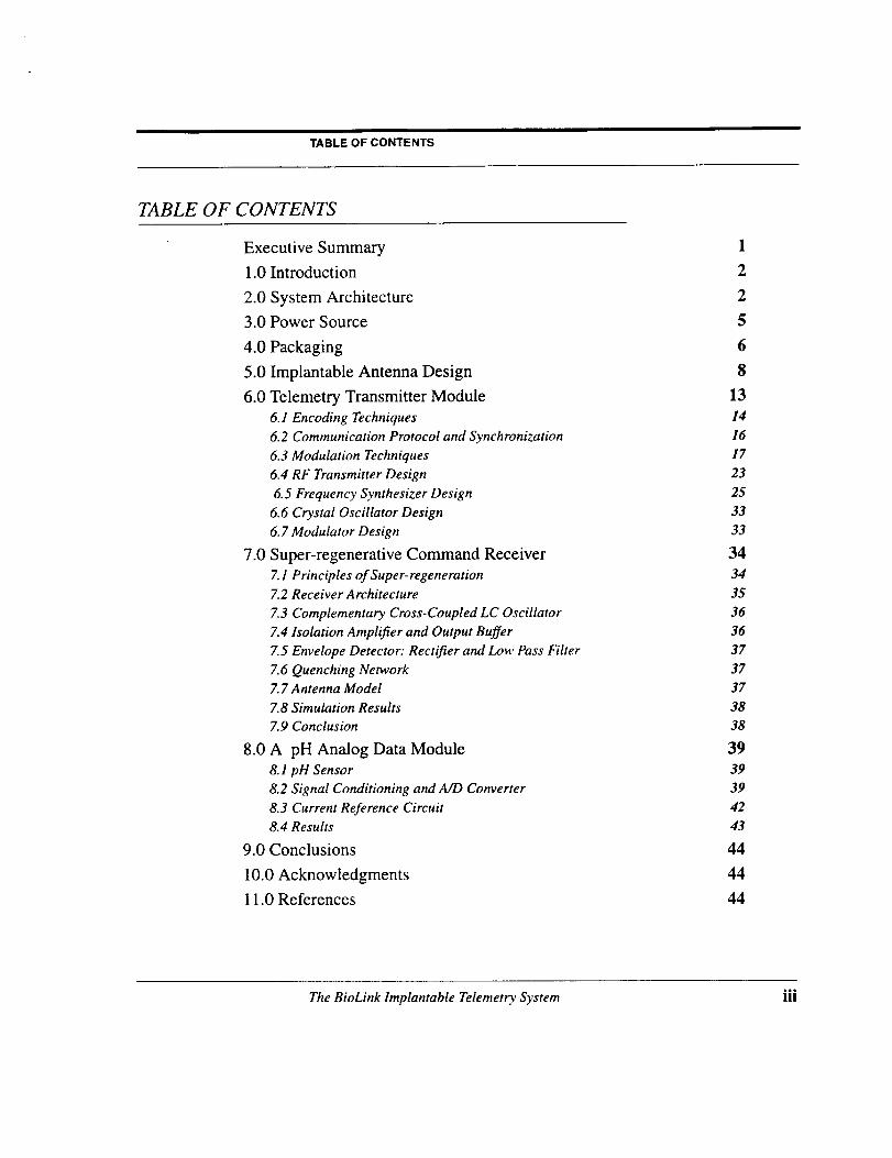
TABLE OF CONTENTS
TABLE OF CONTENTS
Executive Summary
1.0 Introduction
2.0 System Architecture
3.0 Power Source
4.0 Packaging
5.0 Implantable Antenna Design
6.0 Telemetry Transmitter Module
6.1 Encoding Techniques
6.2 Communication Protocol and Synchronization
6.3 Modulation Techniques
6.4 RF Transmitter Design
6.5 Frequency Synthesizer Design
6.6 Crystal Oscillator Design
6.7 Modulator Design
7.0 Super-regenerative Command Receiver
7.1 Principles of Super-regeneration
7.2 Receiver Architecture
Z3 Complementary Cross-Coupled LC Oscillator
7.4 Isolation Amplifier and Output Buffer
7.5 Envelope Detector: Rectifier and Low Pass Filter
7.6 Quenching Network7.7 Antenna Model
7.8 Simulation Results
7.9 Conclusion
8.0 A pH Analog Data Module
8.1 pH Sensor
8.2 Signal Conditioning and A/D Converter
8.3 Current Reference Circuit
8.4 Results
9.0 Conclusions
10.0 Acknowledgments
11.0 References
1
2
2
5
6
8
13
14
16
17
23
25
33
33
34
34
35
36
36
37
37
37
38
38
39
39
39
42
43
44
44
44
The BioLink lmplantable Telemetry System iii

LIST OF FIGURES
FIGURE
FIGURE
FIGURE
FIGURE
FIGURE
FIGURE
FIGURE
FIGURE
FIGURE
FIGURE
FIGURE
FIGURE
FIGURE
FIGURE
FIGURE
FIGURE
FIGURE
FIGURE
FIGURE 19.
1. Overall system architecture of a BioLink-based biotelemetry implant 3
2. Power budget for a typical CMOS PLL frequency synthesizer used in microprocessor
clock generation. 4
3. Frequency-locked loop (FLL) architecture that uses a differential frequencydiscriminator (DFD) 4
4. Eagle-Picher LTC-7P (Li/SOCI 2) discharge characteristic at 20°C 6
5. Saddle package with flexible antenna for rat implants 7
6. Single-turn loop antenna construction and electrical model 9
7. Equivalent circuit for small loop antenna 12
8. Telemetry Module Block Diagram 13
9. QPSK and n/4-QPSK constellation diagram 19
10. Probability of Error vs. EtfN o for ASK, FSK, and PSK modulation schemes 20
11. Class-C RF Output Stage 24
12. QPKS constellation: (a) with AWGN, (b) with AWGN and oscillator phase noise 25
13. Block Diagram of the Frequency-Locked Loop Synthesizer 26
14. FLL Synthesizer uses a Differential Frequency Discriminator 27
15. Differential Ring Oscillator VCO Design 28
16. Oscillator Close-in Phase Noise due to upconversion of thermal and I/f devicenoise 29
17. Ring oscillator waveforms: (a) single-ended output, Vout(t), (b) inpulse sensitivity
function F(tot) 29
t 8. Power dissipation and phase noise for differential ring oscillator using PMOS linear
loads and replica-feedback biasing: (+)Wn=31.tm, (o)Wn=6_tm, (*)Wn=12p.m 30
Differential delay buffer cells: (a) VCO I, clamped-load; (b) VCO 2, symmetric load;
FIGURE 20.
FIGURE 21.
FIGURE 22.
FIGURE 23.
FIGURE 24.
FIGURE 25.
FIGURE 26.
FIGURE 27.
FIGURE 28.
(3) VCO 3, cross-coupled loads
Predicted single-sideband phase noise: (a) VCO 1, (b) VCO 2, (3) VCO 3
Microphotograph of VCO 1with 4 differential buffer delay stages
VCOI transfer characteristic
Pierce Crystal Oscillator Schematic Diagram
Classic Quadrature Modulator Architecture
SS-DQPSK encoder state transition diagram
BioLink Quadrature Modulator Schematic
Simplified diagram of super-regeneration circuit
Oscillation characteristic of super-regenerative receiver
30
31
32
32
33
34
34
35
36
36
iv The BioLink Implantable Telemetry System

LIST OF TABLES
FIGURE 29.
FIGURE 30.
FIGURE 3 !.
FIGURE 32.
FIGURE 33.
FIGURE 34.
FIGURE 35.
FIGURE 36.
Block diagram of super-regenerative receiver 37
Schematic of LC oscillator, isolation amplifier, and output buffer 38
Block diagram of pH Analog Data Module and Biotelemetry Transmitter 39
Schematic for Pulse Width Modulator 40
Simplified diagram for Current Reference 41
Simulated duty cycle vs. input voltage of PWM: (*) Vdd=3.3V, (x) VdO=3.0V, (o)
Vdd=2.7V 42
Simulated Frequency vs. input voltage of PWM: (*) Vdd=3.3V, (x) Vdd=3.0V, (o)
Vdd=2.7V 42
Microphotograph of pH biotelemetry chip 43
LIST OF TABLES
TABLE 1.
TABLE 2.
TABLE 3.
TABLE 4.
TABLE 5.
TABLE 6.
TABLE 7.
TABLE 8.
VHF Industrial, scientific, and medical (ISM) frequency allocation in the UnitedStates. 4
Comparison of primary battery technologies 5
Telemetry Transmitter Module Power Budget 14
BioLink Outlink Packet Format 16
Comparison of various digital modulation schemes 21
Reported Biotelemetry Encoding and Modulation Alternatives 21
Theoretical phase noise and//) d corner frequency for VCO l, VCO 2, VCO 3 31
Summary of simulated results for Super-regenerative receiver 38
The BioLink lmplantable Telemetry System ¥

THIS PAGE INTENTIONALLY LEFT BLANK

The BioLink Implantable Telemetry System
Executive Summary
Most biotelemetry applications deal with the moderated data rates of biological signals. Few people have studied
the problem of transcutaneous data transmission at the rates required by NASA's Life Sciences-Advanced BioTe-
lemetry System (LS-ABTS). Implanted telemetry eliminate the problems associated with wire breaking the skin,
and permits experiments with awake and unrestrained subjects. Our goal is to build a low-power 174-216MHz
RF transmitter suitable for short range biosensor and implantable use.
The BioLink Implantable Telemetry System (BITS) is composed of three major units: an Analog Data Module
(ADM), a Telemetry Transmitter Module (TrM), and a Command Receiver Module (CRM). BioLink incorpo-
rates novel low-power techniques to implement a monolithic digital RF transmitter operating at 100kbps, using
QPSK modulation in the 174-216MHz ISM band. As the ADM will be specific for each application, we focused
on solving the problems associated with a monolithic implementation of the TTM and CRM, and this is the
emphasis of this report.
_hfaearchitecture based on a Frequency-Locked Loop Frequency
(FLL) Synthesizer is presented, and a
rentiai frequency discriminator that eliminates the need for a frequency divider is also shown. A self-
se modulation scheme suitable for low power implementation was also developed. A full system-levelsimulation of the FLL was performed and loop filter parameters were determined. The implantable antenna has
been designed, simulated and constructed. An implant package compatible with the ABTS requirements is also
being proposed.
Extensive work performed at 200MHz in 0.51am CMOS showed the feasibility of integrating the RF transmitter
circuits in a single chip. The Hajimiri phase noise model was used to optimize the VCO for minimum power con-
sumption. Two test chips were fabricated in a 0.5_m, 3V CMOS process. Measured phase noise for a 1.5mW,
200MHz ring oscillator VCO is -80dBc/Hz at 100KHz offset, showing good agreement with the theory.
We also propose a novel superregenerative receiver architecture for implementing the command receiver. The
superregenerative receiver's simplicity, low cost, and low power consumption has made it the receiver of choicefor short-distance data communications, remote control and home automation We present the design of a super-
regenerative AM receiver implemented in a 0.51am CMOS technology that operates at 433.92MHz and dissipates
only 300_W.
Further work entails detailed transistor-level design of the FLL and superregenerative receiver and a monolithic
implementation of an implantable transceiver in 0.5tam CMOS technology.
r
The BioLink Implantable Telemetry System 1

1.0 Introduction
Currently, NASA-Ames Research Center is developing the Life Sciences-Advanced BioTelemetry System (LS-
ABTS) to conduct space-based animal research [NASA95], [Hines95]. In vivo experiments require anesthetizedanimals and hard-wired connections to the implant creating a risk of infection due to transcutaneous wires. Wire
breakage, movement artifacts, ground loops and 60Hz pick-up can also cause problems. NASA requires a low-
power implantable transmitter that can relay biosensor data using an RF digital link in the VHF television band
(174-216MHz). NASA is targeting 2.5KHz of total baseband signal bandwidth equivalent to 100kbps per
implant. Command and control of the unit is achieved through a 433MHz downlink. This design is being pursued
using commercially available components. A low-power highly integrated radio transmitter is key to the success
of this project.
In collaboration with the Fetal Treatment Center at the University of California at San Francisco Medical Center,
NASA is also developing a system for wireless telemetry of physiological parameters of fetuses for monitoring
and identifying distress after pre-natal surgery [Bealer94], [NASA96]. An implant that will monitor heart rate,
temperature, pH, and amniotic fluid pressure is required to operate in-utero for up to 3 months. This application
creates an urgent need for a biotelemetry transmitter for chronic studies of implantable pH sensors. Current
experiments cannot continue beyond 12 days because of wire breakage. BioLink can reduce the cost and extendthe life of such a device.
2.0 System Architecture
Figure 1 shows the overall system architecture of a BioLink-based biotelemetry implant. The amplifer array,
multiplexer, and analog to digital converter (ADC) form the Analog Data Module (ADM).
The Telemetry Module (TM) includes a data buffer, a low-power crystal-controlled frequency synthesizer, a
quadrature phase shift keying (QPSK) modulator, and a differential loop antenna driver. Data is received from the
ADM and a header and CRC block are added by the TM. On command, the RF carrier is modulated with the
resulting bit stream using Differential-QPSK. An RF amplifier drives a small loop antenna to radiate the signal.
The Frequency synthesizer is implemented as a frequency-locked loop, using a 24MHz low-power crystal refer-
ence oscillator. This requires a small external crystal that does not have a major impact on the size of the implant.
A novel switched capacitor differential frequency discriminator (SC-DFD) allows for the selection of the trans-
mit frequency in 3MHz increments in the 174MHz to 216MHz range.
The most important parameter of an implanted biotelemetry system is power dissipation. Power dissipation and
implant lifetime determine the size of the battery which ultimately determines the size of the implant. A signifi-
cant portion of the power budget for any implantable telemetry system is allocated to the generation of the RF
carrier. Given this need for small, low-power wireless devices for biotelemetry, a low-power, integrated fre-quency synthesizer is required.
2 The BioLink Implantable Telemetry System

2.0 System Architecture
Command Receiver Module
l ControlLogic
Super-regenerativeReceiver
Analog Data Module Telemetry Transmitter Module
QPSK RF
-- I M_ r _[_
FIFO
• 200MHz Frequency I I Power &
Synthesizer II Control
FIGURE 1. Overall system architecture of a BioLink-based biotelemetry implant
7
Traditionally, frequency synthesizers have been implemented using a phase-locked loop (PLL). Figure 2 shows
the block diagram and power budget for a state-of-the-art CMOS PLL synthesizer used in microprocessor clock
generation [vonKaene196]. In a PLL synthesizer, the VCO frequency is divided and then compared to a referencefrequency by a phase detector. The phase detector drives a low-pass filter that generate the control voltage for the
VCO. The major sources of power dissipation are the VCO (73%) and the frequency divider (22%). To reduce
power we have to address these blocks first.
We propose a frequency-locked loop (FLL) architecture (fig.3) that uses a switched capacitor differential fre-
quency discriminator (DFD). In the past, quadricorrelators and rotational frequency detectors [Messerschmitt79]
have been used to aid the frequency acquisition process in a PLL, but have been superseded by simpler phase-fre-
quency detectors with charge pumps [Gardner80].
The Command Receiver Module (CRM) provides a mechanism to control remotely the power usage of an
implant in order to extend its useful life. The inlink control channel can change the operating mode (Run,
Standby, and Sleep), transmit frequency, and channel sampling rate. In the Run mode, the implant is fully opera-
tional. During Standby all high frequency circuits are disabled to save power. Sleep mode turns all systems off
except for the receiver and low-frequency clock circuits. The BioLink inlink uses Manchester-encoded Ampli-
tude Shift Keying (ASK) with a 433.92MHz carrier.
The BioLink lmplantable Telemetry System 3

F._ FrequencyPhase
Detector00W_N ChargePump& Loop Filter
101_Ring Fr_._
IPr°g ::emr"b'eI I VCO
- IDivide.by.2I50_
Four
Differential ! _1 Loop Io r u n:,YorI --I Filter
vco
FIGURE 2. Power budget for a typical CMOSPLL frequency synthesizer used inmicroprocessor clock generation.
FIGURE 3. Frequency-locked loop (FLL)architecture that uses a differential frequencydiscriminator (DFD).
We propose a superregenerative receiver architecture for implementing the CRM. The superregenerative receiver,
invented in 1922 by Armstrong [Armstrong22], was eventually supplanted by the superheterodyne receiver
where high performance was required. Still, the superregenerative receiver's simplicity, low cost, and low power
consumption has made it the receiver of choice for short-distance data communications, remote control and home
automation. Recently, a 1.2mW, IGHz superregenerative AM receiver was implemented by P. Farve, et al. in a
0.8Wn BiCMOS technology [Farve98]. Its low power consumption, makes it very attractive for battery-powered
applications. In this report, we present the design of a superregenerative AM receiver implemented in a 0.51am
CMOS technology that operates at 433.92MHz and dissipates only 300_W.
The FCC has authorized unlicensed use of the 38-41MHz, 88-108MHz, 174-216MHz and 433MHz bands for
Industrial, Scientific and Medical (ISM) telemetry purposes [FCC 15] (see Table 1). Other bands in the micro-
wave region (900MHz and above) are not considered because of the high power required to operate at those fre-
quencies. Ideally, the 40MHz band would be used as it is the lowest unlicensed band authorized by the FCC. The
problem with this band is that only 3MHz are allocated making it difficult to accommodate applications requiringmultiple transmitters in a group habitat. The 88-108MHz is usually very congested with FM commercial broad-
casts, leaving only the 174-216MHz VHF television band available for biotelemetry. Up to 14 channels can be
accomodated in this band, easing the selectivity and phase noise requirements of the system.
Frequency (MHz) Bandwidth (KHz)
38-41 200
88-108 200 50 @ 15m
174-216 200 150 @ 30m
Field Strength
QtV/m)
10 @ 15m
Out of bandrequirements (max.)
lO_tWm @ 3m
40_V/m @ 3m
151-tV/m @ 30m
TABLE 1. VHF Industrial, scientific, and medical (ISM) frequency allocation in the United States.
4 The BioLink Implantable Telemetry System

3.0 Power Source
System Zn/HgO Zn/Ag20 Zinc/Air Li/SOCI 2
Cell VoltageEnergy DensityGravimetric
(Wh/kg)
Volumetric
(Wh/L)Advantages
Disadvantages
1.35
100
470
high energy density;flat discharge;stable voltageLow gravimetricenergy density
1.5
120
500
high energy density;good high-rateperformanceLow gravimetricenergy density
TABLE 2. Comparison of primary battery technologies
1.5
340
1050
high energy density;long shelf life(sealed)Not independent ofenvironment
3.65
480
950
high energy density;long shelf life; flatdischargeVery low dischargerate
3.0 Power Source
Power dissipation is the major limiting factor in the performance of a biotelemetry implant. In the past mercury
(Zn/HgO) and silver (Zn/Ag20) oxide cells have been used [Mackay70] and more recently lithium ceils
[Owens86]. Table 2 show a comparison of the best performing primary battery technologies [Linden95]. Even
though Zinc/Air technology offers very high energy density, it requires a source of oxygen, making it unsuitable
for a sealed implant. Lithium thionyl chloride (Li/SOCI 2) batteries have the highest energy density (480Wh/kg)
as well as high cell voltage and long shelf life.
Lithium thionyl chloride (Li/SOCi 2) cells have extremely long storage life (in excess of 10 years) but are capable
of only low-rate discharge. Figure 4 shows the discharge characteristic of the Eagle-Picher LTC-7PN, (Li/SoCI 2)
battery. It is rated at 750mAh, at 3.65V open circuit voltage. For a 2mA discharge rate, we get close to the
expected lifetime of 375 hours, but at a 20mA drain it lasts for only 20 hours. This shows that very small currents
can be drawn for long periods of time, but higher drain reduces significantly the useful life of the battery. The
LTC-7PN has also been fully qualified by NASA for in-flight implantable biotelemetry.
The maximum current drain allowed, given the expected life of the implant is a critical issue for the design of a
telemeter. Current drain limitations have to be considered when allocating the power budget of an implant. For
instance, NASA's LS-ABTS requires 90 hours of implant lifespan for missions that will last up to 90 days.This
constraints the maximum drain for the whole implant to about 5mA. For instance, a BioLink-based ABTS power
budget could allocate up to 2mA for the TM lmA for the CRM, and 2mA for ADM when operating at 100kbps
using the LTC-7PN battery.
For these current drains, the battery might need preconditioning to avoid a prolonged turn-on voltage delay. The
long shelf life of the Li/SOCI 2 cell is a result of the protective LiCI passivation film present on the anode. After
storage, the cell may exhibit a delay in reaching its operating voltage because of the formation of this film. Once
discharge is started, the passivation film is dissipated gradually, and the operating voltage is reached.
The BioLink Implantable Telemetry System 5

4.00
3.50
3.00
2.50
tl ;I I _1ti. l,iIl! : i_
, t ,! ! : !:
! irF!1!1Iiij it! J! llFI' ' _ .... :4 ..... ÷ ..... "'_
1E+O0 1E+01 1E+02 1E+03 1E+04 1E+05
Discharge Time, Hours
FIGURE 4. Eagle-Picher LTC-7P (Li/SOCi2) discharge characteristic at 20°C
The passivation film in the LTC-TPN may be removed more rapidly by the application of high-current pulses fora short time period, or by preconditioning the cell with a 100k_ load for a period of 64 hours. In a sealed
implant, where the battery might be stored for six or more months, it is difficult to precondition the battery just
before its use. Preconditioning is not necessary if the total standby current draw of the implant is about 35pA;
this will prevent the passivation layer from forming, but will also reduce the available capacity by a smallamount.
The size of the battery is also important, as it determines the minimum size of the implant. At 2.66cm 3, and
6.8grams, the LTC-7PN is as large as can be practically accomodated in a rat implant (see Section 4.0 Packag-
ing).
4.0 Packaging
The implant package must provide a moisture barrier to protect the electronics, and must not be toxic or harmful
to the animal. Encapsulation in different kinds of epoxies as well as medical-grade silicone rubber (Silastic), and
conformal coatings such as Parylene are well known. A major concern is sealing the I/O connections to the pack-
age. At Stanford, gold-plated Kovar packages with glass-to-metal feedthroughs were used extensively
6 The BioLink lmplantable Telemetry System
4.0 Packaging
[Knutti83] in the early 1980s, and systems were tested for more than two years using this type of package. In the
past NASA has used machined ceramic packages for implanted telemeters. These are relatively large (7cm dia.),
very expensive to manufacture, and are not readily available.
The package shoud be easy to implant, should cause minimum distress to the animal, and should maximize the
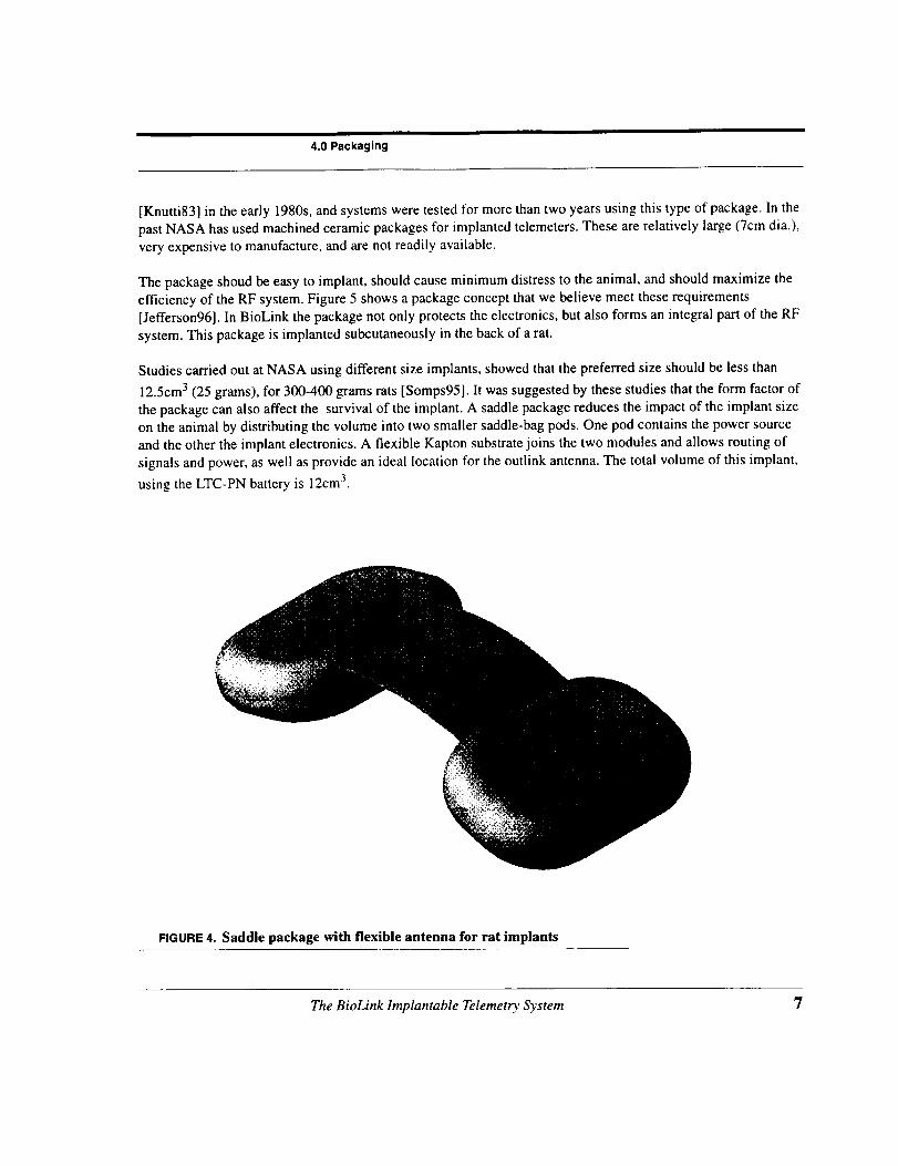
efficiency of the RF system. Figure 5 shows a package concept that we believe meet these requirements
[Jefferson96]. In BioLink the package not only protects the electronics, but also forms an integral part of the RF
system. This package is implanted subcutaneously in the back of a rat.
Studies carried out at NASA using different size implants, showed that the preferred size should be less than
12.5cm 3 (25 grams), for 300-400 grams rats [Somps95]. It was suggested by these studies that the form factor of
the package can also affect the survival of the implant. A saddle package reduces the impact of the implant sizeon the animal by distributing the volume into two smaller saddle-bag pods. One pod contains the power source
and the other the implant electronics. A flexible Kapton substrate joins the two modules and allows routing of
signals and power, as well as provide an ideal location for the outlink antenna. The total volume of this implant,
using the LTC-PN battery is 12cm 3.
FIGURE 4. Saddle package with flexible antenna for rat implants
The BioLink lmplantable Telemetry System 7

Inthisconfigurationtheantennaplacementminimizestheamountoftissuethesignalhastogothrough,andthecorrespondingRFlosses.Also,theflexiblesaddleallowsformaximumlooparea(seeSection5.0),whichmaxi-mizesthesignalcouplingtotheexternalantenna.
TheBioLinkimplantelectronicswillbemounteddirectlytoa1ozrolled-anealedcopper-cladKaptonflexiblesubstrateandconformallycoatedwithParylene.Fiberglassboardstiffeners(FR-4)areusedintheelectronicspodtofacilitatemountingofthecomponents.Thisassemblyisencasedinavacuum-formedmedical-gradeUltemplasticenclosure,andcoatedwithSilastic.TheexposedKaptonbeltinbetweenthepodscontaintheout-linkantennaaswellaspowerleadsfromthebattery.ThisbeltalsoneedstobecoatedwithParyleneandencapsu-latedinSilastic.A Dacronfabricmeshwithsuturehooksisaddedtothebelttoeaseimplantation.Thisprovidesaverylightandruggedencapsulationthatprotectstheelectronicsaswellastheanimal.
5.0 Implantable Antenna Design 1
Any radiating structure produces electrical and magnetic fields. A simple model of a wire carrying a varying cur-rent is described by:
ioLcosO { 1 c _em,.,_d/c;Er = 21r8.o c "_ + jo97d3 J
Eo ioLsinO_j°)¢ c + c 2 le_,,ogt_a/c)= 4 eoc2t d -Z 7g-jd j
H, = i_LsinO4rtc[ d "__J°)_c }ej., t,_d/c)
In the above equations, all l/d terms represent the radiation field component, all l/d 2 terms represent the induc-
tion field component, and all lid 3 terms represent the electrostatic component. These equations describe two
superimposed fields: a "near field" that starts off strong but falls off rapidly with distance, and a weaker "far
field" that changes more slowly. The two become equal at distances from the transmitter of approximately k/6.
At distances a few times this, the electrostatic and inductive fleid components become negligible, and thus the far
field becomes dominant. At a fraction of this distance, the near field is dominant, i.e., more power can be trans-ferred through a near field at short distances than through the radiation field at large distances. At 200MHz,
£-=1.5 meters, and thus the near field dominates inside a small cage, where the maximum transmission distance iswell below ! meter.
1. This work was performed in collaboration with Phillip S. Carter Jr., at Jefferson Laboratories, Inc., Palo Alto, CA, under aNASA-Ames Phase-2 Development Grant for the ABTS Antenna System.
8 The BioLink lmplantable Telemetry System
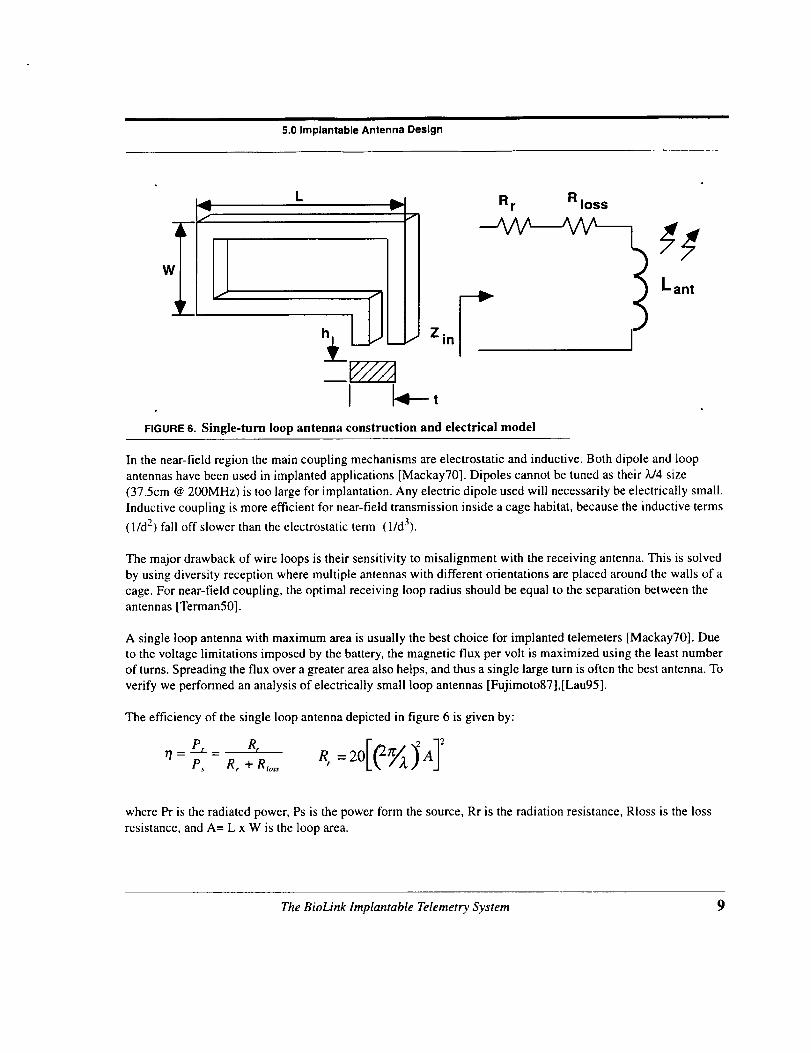
5.0 Implantable Antenna Design
,Jl R r R loss
_l_ Lant
_t z in
FIGURE6. Single-turn loop antenna construction and electrical model
In the near-field region the main coupling mechanisms are electrostatic and inductive. Both dipole and loop
antennas have been used in implanted applications [Mackay70]. Dipoles cannot be tuned as their k/4 size
(37.5cm @ 200MHz) is too large for implantation. Any electric dipole used will necessarily be electrically small.
Inductive coupling is more efficient for near-field transmission inside a cage habitat, because the inductive terms
(1/d 2) fall off slower than the electrostatic term (l/d3).
The major drawback of wire loops is their sensitivity to misalignment with the receiving antenna. This is solved
by using diversity reception where multiple antennas with different orientations are placed around the wails of a
cage. For near-field coupling, the optimal receiving loop radius should be equal to the separation between theantennas [Terman50].
A single loop antenna with maximum area is usually the best choice for implanted telemeters [Mackay70]. Due
to the voltage limitations imposed by the battery, the magnetic flux per volt is maximized using the least number
of turns. Spreading the flux over a greater area also helps, and thus a single large turn is often the best antenna. To
verify we performed an analysis of electrically small loop antennas [Fujimoto87],[Lau95].
The efficiency of the single loop antenna depicted in figure 6 is given by:
[e ]2- Rr "_ AP_-R_+R,o,, R_=20 ¢/'_, ,j
where Pr is the radiated power, Ps is the power form the source, Rr is the radiation resistance, Rloss is the loss
resistance, and A= L x W is the loop area.
The BioLink lmplantable Telemetry System 9

The loss resistance can be represented as:
Rt = _ t where•" 1per
R=_-/O. Lt_ =2(L+W ) Lp,,=2(t+h)
where f is the frequency of operation, c = 5.813 x 10⁷ S/m (conductivity of copper), and Ia = 4p x 10-7 A/m (per-meability of copper), L and W are the length and width of the loop respectively.
We can extend this analysis to a multi-turn loop antenna, by defining the radiation resistance as:
R u=N zx20 A =N 2xR r
where N is the number of turns.
The associated loss resistance is:
and the efficiency of the multi-turn loop is thus given by:
NRRrs = N2Rr _ ......x. for Nl_o,. _ >> N 2R
11= R m + Rios,u N 2R + NRios, - I_o,,
This analysis neglects the proximity effect of closely space turns on the loss resistance. When two loops are
placed close to each other, the proximity effect forces current to the outside edge of each conductor, increasingthe loss resistance. To account for this non-uniform distribution of current along the loop, we redefine:
where Rp is the resistance due to the proximity effect, Ro is the skin-effect resistance per unit length and the ratio
Rp/R o is a function of the spacing ratio (c/a, where 2c is the spacing between conductors and a is the equivalent
wire radius) of the loops [Smith72]. By including the proximity effect on the efficiency calculation, we obtain:
NRr NR r
71-R,os,up-R,o,,(I+Re/Ro)
10 The BioLink lmplantable Telemetry System

5.0 Implantable Antenna Design
The increase in efficiency with the number of turns is offset by the proximity effect. For two-turn loops the effi-
ciency goes up typically by 2dB, but for three or more turns there is no longer a significant benefit.
The radiation resistance is calculated for the far-field, thus the results of this analysis are not completely applica-
ble to the near-field case. In the near-field the ideas of transformer design are more relevant than the usual con-
siderations of radio transmission. Still, this excercise provides some insights on how to maximize the
performance of an antenna. This analysis shows that antenna efficiency increases with the loop area and number
of turns, but at higher frequencies the skin effect limits the useful size of the loop and the proximity effect limitsthe number of turns to one or two.
To complete the antenna model we need to calculate the inductance of the loop, which is given by:
L,.,= (N2-_)x {LlnI" _ (L+ Lc )]+ Wln[" _ (W+ Lc )]+ 2[a+Lc-(L+ W)]}
L =4W2 + L:
and the quality factor of the loop can be calculated using:
jfoZ,,, = f rOa?_t
wherefr is the resonant frequency and 13is the antenna bandwidth. For operation at the 200MHz ISM band, the
required Q is about 6.5.
The antenna impedance is given by:
Z;,, =(R r + R,o,,)+ jO)L..,
This impedance has to be matched to the transmitter in order to maximize the power transfer. The complete
antenna circuit is shown in figure 7 where C I and C2 form a matching network that transforms the input imped-
ance and also resonates the antenna to the operating frequency given by:
1
it-- I2_ L..,_,Q+C2)
The BioLink Implantable Telemetry System 11

R s
R r R loss
Lant
FIGURE 7. Equivalent circuit for small loop antenna
The loaded-Q, when the antenna is matched to the transmitter is given by:
1 ojL
2(R +R,,,.)
and at resonance, the impedance including the matching network is given by:
(g c, + )
By proper selection of Ci and C2, the antenna can be tuned for 200MHz while allowing matching for maximum
power transfer.
The BioLink outlink antenna is built in a flexible Kapton substrate, so our model have to account for the curva-
ture of the loop. The reduction of the effective loop area affects both the radiation resistance and inductance.
Assuming that the antenna is flexed along its width, the curvature correction factor is given by:
Cf I
IT/' ,,/2(1 -cosa)I
W _x
where W' is the effective width for an angle ct, and 0 < cx< 2n.
A small (25 mm x 25mm) two-turn loop was built out of loz (h=341am) copper-clad FR-4 (E=4.8) rigid board
material (l.6mm thick). This antenna was found to be self resonant at 195MHz. This design suffers from exces-
sive parasitic capacitance, due to the construction of the loops with relatively large copper areas (to minimize
Rloss) aligned in opposite sides of the board. Still, using a fixed 56pF chip capacitor in parallel with a high-Q
tubular trimmer (0.6-4.5pF) we were able to tune the antenna to 40MHz. If we neglect the parasitic capacitance,
12 The BioLink lmplantable Telemetry System
6.0 Telemetry Transmitter Module
DATA
Pow r,
FIGURE 8. Telemetry Module Block Diagram
this corresponds to Lant=263nH, which is close to the theoretical value of 200nil. Radiation resistance for a loopthis small is negligible, and the theoretical antenna efficiency approaches zero, thus the main mechanism for sig-
nal propagation is magnetic induction.
An experiment with a 2-turn loop (15mm x 20mm) of AWG.34 wire encapsulated in flexible Kapton tape carried
out at 200MHz showed a difference of 2-8dB in power coupling when flexed with _/2 < a < 2rt/3. Further exper-
iments were carried out to characterize the performance of a flexible loop antenna at 200MHz. Results will be
reported in a future paper.
6. 0 Telemetry Transmitter Module
The Telemetry Transmitter Module (TIM) includes a data buffer, a crystal-controlled frequency synthesizer, a
quadrature phase modulator, and a power amplifier (figure 8). A data packet is first assembled in a FIFO and aheader and CRC block are added by the controller. On command, a packet is serialized and a 174-216MHz car-
rier is modulated with the resulting bit stream using differential quadrature phase shift keying (DQPSK). An RF
power amplifier drives a small loop antenna to transmit the signal. The external RF circuitry is composed of the
loop antenna and its matching network.
The Frequency synthesizer is implemented as a Frequency-Locked Loop, using a 24MHz low-power crystal ref-
erence oscillator. It generates both In-phase and Quadrature outputs necessary for QPSK modulation. A pro-
grammable differential frequency discriminator (DFD) allows for the selection of the transmit frequency in3MHz increments in the 174MHz to 216MHz range.
The BioLink lmplantable Telemetry System 13
Module
TTMSubsystem
FLL Synthesizer & RF Amp24 MHz crystal oscillatorQPSK encoder/modulatorData Buffer
ADM interface
Control LogicTotal TTM
Imax (pA)1000
10550o
10020o
2o0
2105
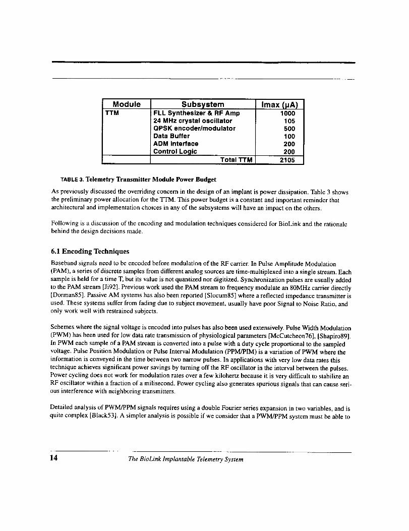
TABLE 3. Telemetry Transmitter Module Power Budget
As previously discussed the overriding concern in the design of an implant is power dissipation. Table 3 shows
the preliminary power allocation for the TTM. This power budget is a constant and important reminder that
architectural and implementation choices in any of the subsystems will have an impact on the others.
Following is a discussion of the encoding and modulation techniques considered for BioLink and the rationalebehind the design decisions made.
6.1 Encoding Techniques
Baseband signals need to be encoded before modulation of the RF carrier. In Pulse Amplitude Modulation
(PAM), a series of discrete samples from different analog sources are time-multiplexed into a single stream. Each
sample is held for a time T, but its value is not quantized nor digitized. Synchronization pulses are usually added
to the PAM stream [Ji92]. Previous work used the PAM stream to frequency modulate an 80MHz cartier directly[Dorman85]. Passive AM systems has also been reported [Slocum85] where a reflected impedance transmitter is
used. These systems suffer from fading due to subject movement, usually have poor Signal to Noise Ratio, and
only work well with restrained subjects.
Schemes where the signal voltage is encoded into pulses has also been used extensively. Pulse Width Modulation
(PWM) has been used for low data rate transmission of physiological parameters [McCutcheon76], [Shapiro89].
In PWM each sample of a PAM stream is converted into a pulse with a duty cycle proportional to the sampledvoltage. Pulse Position Modulation or Pulse Interval Modulation (PPM/PIM) is a variation of PWM where the
information is conveyed in the time between two narrow pulses. In applications with very low data rates this
technique achieves significant power savings by turning off the RF oscillator in the interval between the pulses.
Power cycling does not work for modulation rates over a few kilohertz because it is very difficult to stabilize an
RF oscillator within a fraction of a milisecond. Power cycling also generates spurious signals that can cause seri-ous interference with neighboring transmitters.
Detailed analysis of PWM/PPM signals requires using a double Fourier series expansion in two variables, and is
quite complex [Black53]. A simpler analysis is possible if we consider that a PWM/PPM system must be able to
14 The BioLink lmplantable Telemetry System

6.0 Telemetry Transmitter Module
resolve the minimum pulse width x produced by the encoder. The spectrum of a periodic pulse sequence with
amplitude Am, period T, and pulse width x is given by
f(t) =2 lc.lcos(co./)Z n=l
where and
si _ n'C
forn= 1,2,3 ...
The spacing between harmonics is 2n/T. As T decreases the harmonics move farther apart. As the pulse width "_decreases, the first zero crossing moves out in frequency. For x << T most of the signal energy will lie in the
range 0 < O n < 2r./x. The bandwidth (to the first zero crossing) is thus defined by
2n:fo-
For example, to transmit 25,000 8-bit samples per second using PWM would require
f __
1 1
-T_2S/-25x103x256=6.4MHz"L"
These pulse techniques, even though adequate for low data rates, are impractical for signals above a few kilo-
Hertz due to the excessive bandwidth required.
In Pulse Code Modulation (PCM), a PAM stream is quantized and digitized by an Analog to Digital converter
(ADC). The resulting bit stream is further encoded and shaped to suit the synchronization and RF modulationmethods used further downstream. Several PCM biotelemetry systems have been reported in the literature
[Fryer74], [Leung86], [Cupa189].
Some advantages of PCM include greater noise immunity and robustness to channel impairments, easier multi-
plexing of various channels, and ability to accomodate digital error-control codes. PCM also supports complex
signal conditioning techniques such as source coding, encryption and equalization to improve the overall perfor-mance of the link. Due to its many advantages over analog encoding techniques, PCM encoding is the method of
choice for BioLink.
The BioLink lmplantable Telemetry System 15

Packet Field
1010 1010 1010 10
11
RRRR
BBBB
CC
SSSS SSSS
eee
Definition
14-bit Preamble
2-bit Start of Frame Delimiter
4-bit Rodent Identification Number
4-bit BioLink ID Number
2-bit Error Control Field
8-bit Sample Data Field
(repeat for 8 channels)
TABLE 4. BioLink Outlink Packet Format
6.2 Communication Protocol and Synchronization
Synchronization is achieved by sending data as packets using a protocol similar to those proposed by M. Geisler
[Geisler95], and the IEEE 802.3 standard. Each packet is made up of a header, data block, and error control block(Table 4).
The Header consists of a Packet Preamble (PP), Packet Type (PT), Rodent Identification Number (RID), andBioLink Identification Number (BID). The Packet Preamble allows the external receiver to detect the carrier and
synchronize with the incoming packet. It consists of an alternating 1,0 pattern followed by the Start of Frame
Delimiter (SFD) consisting of two consecutive l's. The Type Field identifies the packet as being either Status or
Data. The Rodent and BID numbers uniquely identify the implant. The CRM has a separate programmable regis-
ter that holds the Packet Type, Rodent Number and BIN. These are automatically added to the packet duringtransmission.
The data block consists of 8 data words with 10 bits each. Each word has a 2-bit Error Control (EC) field and a 8-
bit Data Field (DF). Data is received from the ADM into a buffer on the TTM, and when commanded, a header is
attached, Checksum is generated, and the RF power circuits are energized to send the packet.
The EC field is a 16-bit Cyclic Redundancy Check (CRC) word calculated and appended to a packet during
transmission. During reception, error-free packets result in a specific pattern in the CRC generator. Packets with
improper CRC are rejected. Bit synchronization is implemented in the QPSK modulator and is an integral part ofthe Self-Synchronizing DQPSK modulation technique described in Section 6.3.6.
16 The BioLink lmplantable Telemetry System

6.0 Telemetry Transmitter Module
6.3 Modulation Techniques
Modulation theory provides insights on the basic tradeoff of transmitter power efficiency versus bandwidth effi-
ciency. Modulation design is primarily concerned with the tradeoff of signal power versus error rate over a band-
limited noisy channel. This provides an insight into saving transmitted signal power, which saves battery power
and prolongs the lifetime of the implant. In Section 6.4.1, it is demonstrated that the transmitted power is just a
fraction of the total power required by the transmitter to generate the RF carrier. Thus, the criteria for selecting a
modulation scheme is based on maximizing the practical power efficiency which includes the biasing of the cir-
cuits used in its implementation. Following is a brief review of the modulation techniques available for biotelem-
etry and a comparison of their theoretical power efficiency.
6.3.1 Amplitude Shift Keying (ASK)
Is a special case of Amplitude Modulation where the binary values are represented by two different amplitudes of
the carrier frequency can be described by:
Acos(CO_ t) b = 1fc(t) =
0, b =0
Taking the Fourier transform, we obtain:
A [F(c0 - coc )+ F(Co + 0Jc )]FXo ) = 7
The effect is to shift the spectrum of the baseband signal up to frequency coc with symmetrical sidebands around
o_c. The transmission bandwidth is twice the initial baseband bandwidth.
6.3.2 Frequency Shift Keying (FSK)
The carrier alternates between two frequencies, where e01 corresponds to a binary 1, and ¢o2 to a binary 0, and
can be described by
f<(t)= "Ac°s(O)lt)'b = 1 ,for - % <, <
Acos(Co2t),b = 0
where T is the baseband pulse width. The frequency spectrum of FSK is difficult to obtain. A special case usinga sequence of alternating l's and O's leads to a good rule of thumb for FM bandwidth and is much easier to evalu-
ate [Schwartz80]. If the two frequencies are synchronized in phase and given by
f, :%, and f2 :n/T,
The BioLink Implantable Telemetry System 17

where m,n are integer, then the spectrum is given by
sin [(c0,- o9 )T//2] +(r..o,- 09.)T//2 (-1)"
sin [(o92- o_.)T//2]
(092 -fo, )T//2 ' where o9, :/rt)/T
The spectrum can be visualized as two superimposed periodic ASK signals. The bandwidth (to first zero cross-
ing) is then
B, = 2B(1 + fl)
where B is the baseband bandwidth. The parameter 1_is defined as
B B
where Af is called the frequency deviation. This result is also known as Carson's rule. If Af>>B, the bandwidth
approaches 2Af, and it is called wideband FM. The bandwidth is essentially independent of the baseband band-width. For Af<<B. the bandwidth approaches 2B, and is called narrowband FM. The bandwidth is essentially the
same as for ASK, and is determined by the baseband signal. The minimum spacing required for noncoherentdetection of FSK is 1/T Hertz.
It is the expansion of transmission bandwidth that increases the noise immunity, thus narrowband FSK does not
have a SNR advantage over ASK. FSK's constant envelope has an advantage when transmitting through a nonlin-
ear channel, and although implementing ASK is simple, it has relatively poor error performance and susceptibil-
ity to fading and nonlinearities [Smith93].
6.3.3 Binary Phase Shift Keying (BPSK)
The phase of a constant amplitude carrier is switched between two values corresponding to binary l and binary 0
respectively. The two phases are separated by 180 degrees, and can be described by
f c( t)= m(t)cosOgct,for -T//2 < t < T//2,
where T is the baseband pulse width, and re(t) has values of+l for a binary 1, and -1 for a binary 0. BPSK is
equivalent to a double-sideband suppressed carrier amplitude modulation, where cos Oct is the carrier and re(t) is
the modulating signal. It has the same double-sideband characteristic as ASK, where the bandwidth is twice that
of the baseband signal, centered at the carrierfc.
18 The BioLink lmplantable Telemetry System
6.0 Telemetry Transmitter Module
1,1B
1,1A
QPSK
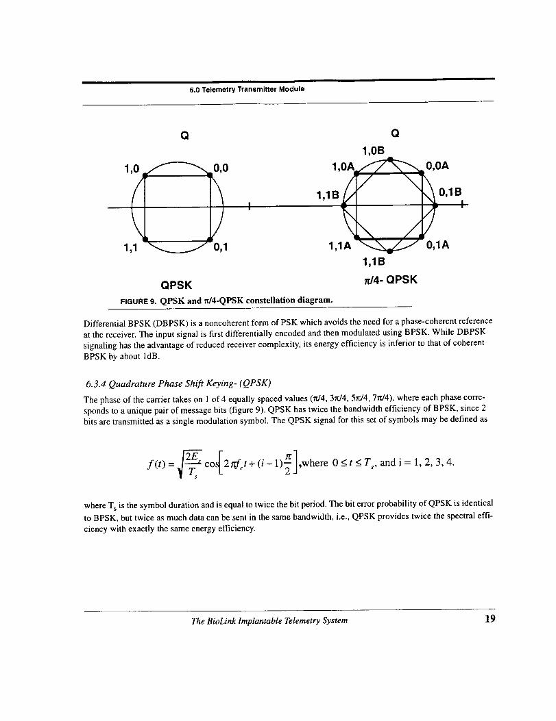
FIGURE 9. QPSK and _J4-QPSK constellation diagram.
Q
1,0B
1,1B
_/4- QPSK
0,0A
0,1B
0,1A
Differential BPSK (DBPSK) is a noncoherent form of PSK which avoids the need for a phase-coherent reference
at the receiver. The input signal is first differentially encoded and then modulated using BPSK. While DBPSK
signaling has the advantage of reduced receiver complexity, its energy efficiency is inferior to that of coherent
BPSK by about ldB.
6.3.4 Quadrature Phase Shift Keying- (QPSK)
The phase of the carrier takes on 1 of 4 equally spaced values (rd4, 3_/4, 5n/4, 7rd4), where each phase corre-
sponds to a unique pair of message bits (figure 9). QPSK has twice the bandwidth efficiency of BPSK, since 2
bits are transmitted as a single modulation symbol. The QPSK signal for this set of symbols may be defined as
= co 2zrfct + (i- 1) ,where 0 < t < Ts, and i = 1, 2, 3, 4.
where T s is the symbol duration and is equal to twice the bit period. The bit error probability of QPSK is identical
to BPSK, but twice as much data can be sent in the same bandwidth, i.e., QPSK provides twice the spectral effi-
ciency with exactly the same energy efficiency.
The BioLink lmplantable Telemetry System 19
6.3.5 Modulation Tradeoffs: Power, Noise and Bandwidth
Modulation design is primarily concerned with maximizing the bandwidth efficiency, and minimizing the power
required for transmission while maintaining an acceptable bit error rate (BER). The most important parameter indetermining the performance of a digital communication system is the signal to noise ratio (SNR). SNR isdefined by
(S/N)d B = lOlog _
N power
which is the ratio of signal power to noise power in a given bandwidth.
Shannon showed that the theoretical maximum channel capacity, in bits per second (bps) is given by
c = 81oo (1+s/N)
where B is the channel bandwidth in Hertz [Shannon49]. In practice, however, only much lower rates are achiev-
able, as this formula only accounts for thermal noise. It can be seen how the SNR determines the upper bound onthe achievable data rate.
100
10 -1
¢-_
.10 -2
2
10-3
0
,-_>'1o-4
..Q
10 -5
10 -6
10 -7 ! | I
0 5 10
Eb/No (dB)15
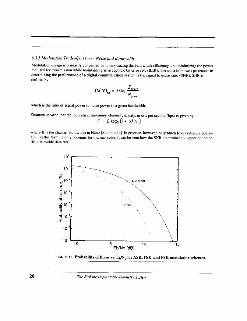
FIGURE 10. Probability of Error vs. Eb/N o for ASK, FSK, and PSK modulation schemes.
20 The BioLink lmplantable Telemetry System

6.0 Telemetry Transmitter Module
Bandwidth BW Efficiency, RfB Eb/NoModulation
(200kbits/sec) (bits/Hz) (BER=10.6)
ASK 400KHz 0.5 13.5dB
FSK 400KHz 0.5 13.5dB
BPSK 400KHz 0.5 10.5dB
QPSK 200KHz 1.0 10.5dB
TABLE 5. Comparison of various digital modulation schemes
A parameter related to SNR is the ratio of signal energy per bit to noise energy per Hertz, Eb/N o. This ratio is
defined as
e /N = (S/ NXe B)
where R is the bit rate, and the ratio (R/B) is the bandwidth efficiency. Eb/N o is important because the bit error
rate (BER) is a decreasing function of this ratio. As the bit rate R increases, the transmitted signal power, relative
to noise, must increase to maintain the required Eb/N o.
Figure 10 shows the probability of bit error Pe versus Et,/N o for ASK, FSK, BPSK and QSK modulation
schemes, assuming coherent detection. As Eb/N o increases, the error rate drops. For Pe less than 10 -5, BPSK/
QPSK show a 3dB advantage in SNR over ASK/FSK.
Table 5 compares ASK, FSK, BPSK and QPSK modulation methods for a 200kbps data rate and BER=10 -6.
ASK and FSK have the same Eb/N o performance as well as the same bandwidth efficiency. Both BPSK and
QPSK have a 3dB advantage over ASK/FSK, and QPSK is clearly superior with twice the bandwidth efficiencyof BPSK.
Encoding Analog Modulation Digital Modulation
AM FM ASK FSK BPSK QPSK
PAM [Slocum85] [Dorman851
FM [Jeutter83]
PPM
PCM
[Henry92]
[Hines95] [Jeutter95]
TABLE6. Reported Biotelemetry Encoding and Modulation Alternatives
[Fernald92] BioLink
The BioLink lmplantable Telemetry System 21

The transmitted signal power represents just a fraction of the total power required by the TIM. The choice of a
modulation scheme should maximize the power efficiency accounting for the power allocation to other sub-
systems within the "VIM. For instance, a QPSK modulator represents only 6.2% of the total power budget.
Assuming that a simpler ASK/FSK modulator that dissipates no power is used instead, this would represent sav-
ings of only 0.28dB of the TrM budget. Thus, the choice of a modulator is strongly influenced by ease of imple-
mentation, and maximum SNR, not as much by theoretical power efficiency of the modulation scheme used.
BioLink use of Differential-QPSK is described in the next section. Table 6 shows how BioLink fits within the
design space of encoding and modulation techniques reported in the implantable biotelemetry literature. BioLink
is the first implantable biotelemetry system to use PCM/QPSK.
6.3.6 Self-Synchronizing Differential QPSK
The Self-Synchronizing Differential QPSK (SS°DQPSK) modulation scheme 2 combines data encoding and car-
rier phase modulation in one operation. This simplifies the hardware required for the modulator and reduces
power dissipation.
To understand SS-DQPSK, it is useful to study the _4-DQPSK modulation scheme used by the U.S. Digital Cel-
lular system (EIA IS-54 standard). In a n/4-DQPSK modulator, signaling points are selected from two orthogo-
nal QPSK constellations (figure 9). Switching between the two constellations every succesive bit ensures that
there is at least a phase shift which is an integer multiple of _/4 between succesive symbols. This ensures thatthere is a phase transition for every symbol, which enables a receiver to perform timing recovery and synchroni-zation.
BioLink scales the rd4-DQPSK scheme to a level more appropriate for low-power biotelemetry using two con-
stellations with two signaling elements each, for a total of 4 phases. In SS-DQPSK, a binary 1 is transmitted as a
+m'2 phase shift, and a binary 0 is represented by a -n/2 phase shift, thus ensuring a phase transition on every
symbol. This scheme solves the problem of bit synchronization, as the bit clock is encoded in the phase shift. The
encoder can be implemented with a simple 2-bit up/down counter, which uses very little power. The SS-DQPSKmodulator essentially combines a DQPSK modulator with a bi-phase differential data encoder.
Differential encoding reduces the power efficiency by ldB, but eliminates the problem of phase synchronizationat the receiver. Power is saved transmitting packets in short bursts, by minimizing the time required by the
receiver to acquire carrier lock. Bandwidth efficiency is reduced in half, because of the signal clock encoding, but
this allows for a very robust and simple synchronization mechanism. Bandwidth efficiency of other modulation
schemes would also be reduced in half if the signal is bi-phase (Manchester) encoded before modulation.
2. Also known as symmetric-QPSK [Hickman93].
22 The BioLink lmplantable Telemetry System

6.0 Telemetry Transmitter Module
6.4 RF Transmitter Design
BioLink uses an integrated class-C power amplifier to drive the antenna. The external RF circuitry is composed
of a loop antenna and its matching network. This section discusses the selection of the operating frequency, spec-
trum allocation, link budget, and implementation issues of the RF power amplifier.
6.4.1 RF Spectrum Allocation
The most important issue of an implanted biotelemetry system is power dissipation. While VLSI circuits can
help reduce the size of the implant, power dissipation and expected implant lifetime determine the size of the bat-
tery which ultimately determines the size of the implant. To minimize the power of a transmitter, we have to
select the lowest practical RF carrier frequency, as RF circuits dissipate power that is proportional to their operat-
ing frequency.
The FCC has authorized unlicense use of the 38-41MHz, 88-108MHz, and 174-216MHz Very High Frequency
(VHF) bands for Industrial, Scientific and Medical (ISM) telemetry purposes [FCC 15]. Other bands in the micro-
wave region (900MHz and above) are not considered because of the high power required to operate at those fre-
quencies. As shown in Table 1, regulations limit the allowable RF field strength to minimize the interference with
other authorized broadcasts. A major concern is also the effect on tissue of a strong RF field. To avoid tissue
damage due to RF heating, the maximum RF power density should not exceed 10mW/cm 2 [Neukomm76].
These constraints are not difficult to meet given that the required transmitted power is in the order of microWatts
for experiments with caged small-animals.
Ideally, the 40MHz band would be used as it is the lowest unlicensed band authorized by the FCC. The problem
with this band is that only 3MHz are allocated making it difficult to accomodate the high data rates required by
neural signal telemetry. This is also unsuitable for low-rate applications requiring multiple transmitters in a group
habitat. The 88-108MHz is usually very congested with FM commercial broadcasts, leaving only the 174-
216MHz VHF television band available for biotelemetry. Up to 14 neural-grade channels can be accomodated in
this band, easing the selectivity and phase noise requirements of the system.
In the BioLink system, the 174-216MHz ISM band is divided into 14 channel slots, each 3MHz apart. Every
other slot is occupied, providing up to 7 simultaneous channels for a frequency-division multiple-access (FDMA)
scheme. Having 3MHz of spacing between channels relaxes the requirements on the transmitter's phase noise
and the external receiver's selectivity.
6.4.2 Link Budget and Transmitter Power
A first order analysis can be performed to determine the power required for the transmitted RF signal. The trans-
mitter power Pt is given by
P, = Lp + kTo + 10 log R + Nj + E_/No
The BioLink lmplantable Telemetry System 23

IN4.6pF
m
Vdd
54/4
FIGURE 11. Class-C RF Output Stage
4000/2
_]__C=,43pF
v0 ¢¢) L ant
Lbond _ 340nil
...J__. Cpa d ,...L_. Cpi n
_lpF _'_ 3pF
where Lp is the transmission loss through tissue and air, kTo is -172.6dBm/Hz at body temperature (37°C), R is
the data rate, and Nf is the receiver's noise. If we assume that Nf is 7dB, and Lp is 75dB [Fotowat84] for a data
rate of 200kbps using QPSK modulation with a desired BER of 10 -6, then
P, = 75 - 172.6 + 101og(200x103)+ 7 + 10.5 = -21.1dBm = 7.7//W
This analysis gives a lower bound on the RF power output of the transmitter. In contrast, the BioLink VCO uses
about 1.5mW to generate a 200MHz carrier. This clearly shows that the biasing requirements of the transmitter
circuit, more than the actual power radiated, determine the power drain of the implant.
6.4.2 RF Power Amplifier
The basic trade-off is between power and range for a given SNR. An active transmitter, where an implanted RF
source is used is the most common solution [Knutti83]. Active AM transmitters require a Class-A or Class-AB
output stage (50-75% efficiency) due to iinearity requirements [Hardy79]. These are not as efficient as the class-
C amplifiers (up to 90% efficiency) usually used with FM transmitters. Performance is also affected by loading
of biological materials on the antenna which can "pull" the frequency of the RF oscillator [Dorman85]. Using abuffered class-C output (figure I I ), BioLink does not suffer from frequency "pull."
24 The BioLink lmplantable Telemetry. System

6.0 Telemetry Transmitter Module
°, • "_, • • •
• , °,, ; v_,Oo
FIGURE 12. QPKS constellation: (a) with AWGN, (b) with AWGN and oscillator phase noise
6.5 Frequency Synthesizer Design
Frequency synthesizers provide the precise reference frequencies for modulation and demodulation of RF sig-
nals. All practical frequency sources have undesirable phase fluctuations due to intrinsic device noise. Phase
noise is particularly important in RF systems as it can lead to (1) increased bit error rates (BERs) in digital com-
munication systems, (2) contamination of adjacent frequency channels and (3) receiver desensitization due to
reciprocal mixing where out-of-band signals are translated into the IF [Crawford94].
In a typical digital communication system, phase noise in the local oscillator can cause the signal constellation to
rotate in a random fashion, thereby degrading the BER performance. As an example, Figure 12 shows the effectsof noise on the constellation for a QPSK modulated signal, where (a) shows the effect of additive white gaussian
noise (AWGN), while (b) adds the effect of phase noise at the carrier frequency. The noise have been exaggerated
for illustration purposes. It shows how phase noise increases the probability of error in the detection of the signal
by skewing the constellation thus reducing the effective distance between the symbols.
Traditionally, frequency synthesizers have been implemented using a phase-locked loop (PLL). Figure 2 shows
the block diagram and power budget for a state-of-the-art CMOS PLL synthesizer used in microprocessor clock
generation [vonKaene196]. In a PLL synthesizer, the VCO frequency is divided and then compared to a reference
frequency by a phase detector. The phase detector drives a low-pass filter that generate the control voltage for the
VCO. The major sources of power dissipation are the VCO (73%) and the frequency divider (22%). To reduce
power we have to address these blocks first. An alternative frequency-locked loop (FLL) synthesizer architecture
has been proposed [Betancourt97], that eliminates the need for a frequency divider. A block diagram of the syn-
thesizer is shown in figure 13.
A FLL synchronizes a voltage controlled oscillator (VCO) with a reference signal in frequency. In the synchro-
nized state the frequency difference between the VCO's output and the reference is ideally zero. If a frequency
error builds up, a feedback mechanism acts on the VCO to reduce the frequency difference. The frequency of the
The BioLink Implantable Telemetry System 25

DifferentialF_ Frequency
Discriminator
,J F°uT I Vo(s) =
FOUT(S) = K v. Vc(s)
Vo Loop Filter
Vc LF(s) ]Kb "(FREF- ForT) = s'_
[Ring[....Vco.....I.........I
FIGURE 13. Block Diagram of the Frequency-Locked Loop Synthesizer
VCO is thus synchronized or locked with the frequency of the reference signal, and that is why this is called a
Frequency-Locked Loop.
We propose a frequency-locked loop (FLL) architecture that uses the differential frequency discriminator (DFD)
shown in figure 14. In the past, quadricorrelators and rotational frequency detectors [Messerschmitt79] have been
used to aid the frequency acquisition process in a PLL, but have been superseded by simpler phase-frequency
detectors with charge pumps [Gardner80] that require frequency dividers in the loop. The proposed FLL does not
require a frequency divider, which represents 22% of the power budget for the PLL example just shown. The
FLL can perform frequency comparison directly without a divider (N= 1) by using a DFD implemented with
switched capacitor circuits.
B ioLink synthesizes the 174-216MHz RF carrier from a low-power 24MHz crystal oscillator using a frequency-
locked loop (FLL). In BioLink, quadrature carriers are generated by a differential ring oscillator VCO. A
switched capacitor differential frequency discriminator (DFD) compares the crystal reference to a scaled down
version of the VCO frequency. The output of the DFD is filtered by a simple l-pole filter, 1/sC. The filtered out-
put controls the biasing of the VCO, thus closing the loop. For a 0.5_m CMOS process, the VCO and crystal
oscillator, use 5001JA, and 1001.tA respectively at 3V. The whole synthesizer consumes about 6001aA.
6.5.1 FLL Frequency Synthesizer Model
The closed-loop signal diagram for the FLL is shown in figure 13, and its phase transfer function is given by
FO_..___T 1 where (oN KV" KDFREF (s) - l + s/(o N - C
26 The BioLink lmplantable Telemetry System

6.0 Telemetry Transmitter Module
M, M21 ,I vco
M5 f "_ CI C2
FIGURE 14. FLL Synthesizer uses a Differential Frequency Discriminator.
This function describes a first order system with one pole, where, Kv is the frequency to voltage transfer charac-
teristic of the VCO, and KD is the capacitor ratio of the DFD. A linear analysis shows that this system is inher-
ently stable (neglecting sample-data effects).
6.5.2 Switched Capacitor Differential Frequency Discriminator Design
The differential frequency discriminator (DFD) is shown in figure 14. In operation, current I I is generated by
switches S 1, S 2 and capacitor C I, and is inversely proportional to the reference frequency driving the switches,
FREF, and the value of C 1. Current 12 is also inversely proportional to the feedback frequency, and the value of
C 2. Current mirror MI/M 2 force these two currents to be equal, resulting in the following relationship:
C 1
Fo, t = -_2" Fref
where the output frequency is determined solely by the capacitor ratio, CI/C 2.
6.5.3 Voltage-Controlled Oscillator Design
The VCO's power dissipation is determined by the frequency of operation and the phase noise performance
required. Power dissipation at a given frequency cannot be made arbitrarily small, as it is constrained by the
choice of technology, and by the system's phase noise requirements. VCO design is critical in the performance of
the synthesizer, as the phase noise at the output of the FLL is solely a function of the phase noise of the VCO.
This section presents a design methodology for differential ring oscillators suitable for FLL frequency synthesis,
The BioLink lmplantable Telemet O, System 27

VcVdd
_ :: _ I V -I_F
Vbias __Ir]Vbias
FIGURE 15. Differential Ring Oscillator VCO Design
IFF
that trades off power dissipation with phase noise. This methodology uses a new phase noise model to trade-off
phase noise and power dissipation in the design of ring oscillators. We compare the theoretical phase noise per-
formance of three buffer stages using clamped, symmetric and cross-coupled loads, respectively. We propose a
cross-coupled buffer topology that achieves lower phase noise by exploiting symmetry. This achieved a 95%
reduction in the l/fl corner frequency of the phase noise characteristic.
Selection Criteria for Oscillator Topology
In general, higher Q oscillators posses lower phase noise. Crystal oscillators have excellent phase noise charac-
teristics, but are not suitable for tunable oscillators. Resonant LC oscillator also have very good phase noise per-
formance, but require inductors that are difficult to implement in monolithic form. Monolithic inductors at
200MHz require large die areas and suffer from low Qs, which makes them unpractical for integration. Ring
oscillators are often used as VCOs in monolithic PLL implementations. The ring oscillator has the worst phase
noise performance of all VCO alternatives, but it is easy to integrate, and can run at very high frequencies with
low power dissipation. In biotelemetry, data rates are low, and channel spacing wide, relaxing the phase noiserequirements. This makes it feasible to use voltage-controlled ring oscillators which are easy to integrate and do
not require any external components.
Power vs. Frequency Trade-off
For a differential ring oscillator, the total power dissipation is given by
P = NlddVad
where N is the number of stages, lad is the tail current of the differential pair, and Vdd is the supply voltage. The
frequency of oscillation can be approximated by
f- 2NCLVs
where C L is the load capacitance and V s is the maximum single-ended voltage swing at the output of each stage.
28 The BioLink lmplantable Telemetry System
6.0 Telemetry Transmitter Module
L(Af)dBc/H;
±
FNoise
--"-Af
FIGURE 16. Oscillator Close-in
Phase Noise due to upconversionof thermal and 1/fdevice noise
Y-h Y-h Y-h._L2 L_2 L2 "-
A AV V V v
FIGURE 17. Ring oscillator waveforms; (a) single-ended output, Vo.t(t), (b) inpulse sensitivityfunction I'(o_t)
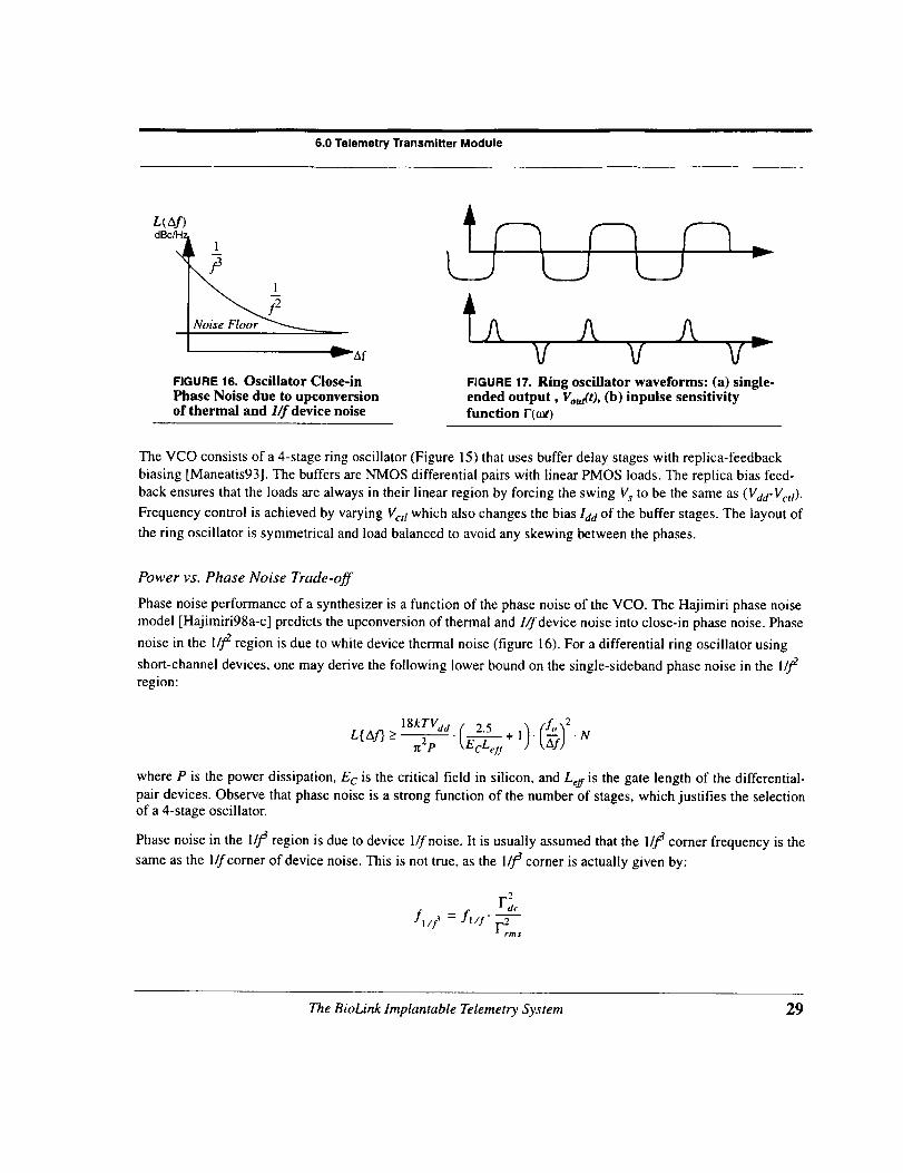
The VCO consists of a 4-stage ring oscillator (Figure 15) that uses buffer delay stages with replica-feedback
biasing [Maneatis93]. The buffers are NMOS differential pairs with linear PMOS loads. The replica bias feed-
back ensures that the loads are always in their linear region by forcing the swing Vs to be the same as (Vdd-Vctl).
Frequency control is achieved by varying Vct ! which also changes the bias lad of the buffer stages. The layout of
the ring oscillator is symmetrical and load balanced to avoid any skewing between the phases.
Power vs. Phase Noise Trade-off
Phase noise performance of a synthesizer is a function of the phase noise of the VCO. The Hajimiri phase noise
model [Hajimiri98a-c] predicts the upconversion of thermal and l/f device noise into close-in phase noise. Phase
noise in the 1/_ region is due to white device thermal noise (figure 16). For a differential ring oscillator using
short-channel devices, one may derive the following lower bound on the single-sideband phase noise in the I/p
region:
18kTVaa ( 25 l_.(fo'_ 2L{Af}>_ -- . -'- + ) _-_f)2p _EcLe/f
N
where P is the power dissipation, E c is the critical field in silicon, and Le# is the gate length of the differential-
pair devices. Observe that phase noise is a strong function of the number of stages, which justifies the selection
of a 4-stage oscillator.
Phase noise in the l/j d region is due to device I/f noise. It is usually assumed that the 1/3d corner frequency is the
same as the I/f corner of device noise. This is not true, as the 1/j"d corner is actually given by:
2Fac
f|lf_ = fill" F 2rills
The BioLink Implantable Telemetry System 29

= w;,=3u_,I iWn=6um _ .... ,,
15 ...... Wn=12umt Zi_i ! i!:: "
.
5
i_ 0 .......
i........._15 rf - i:-; . :, ; _ilii; : ' ::;;4
10 _ 101 10 _ 10
Frequency, MHz
-80 ..... ,.__., : : : : :
N / I Wn=6um / i : i _ _,,,,_i ; : : : : ;:
-ss_ • wn=12uml .i _:_i .... i i i iii;-"o ] _ _ ][![]] ] [ _.:[[_: .
v -9o _ _ _ +_--_ _ [.._'E_ ..... :
-_s .... _)-,_'..._. i .i.i.!,i.i_i ,. i-! i '.i,.i_•_ i _ ii_._;:i :; i li! ::ii i i il _i:
,_-_oo .... i .._. i .i i i iii .... i. i .i i i i i:i ..... _ i : i _i,
• i i ]!:_iii: i i :: :.i!iT:: : : : !:
501 101 10 _ 10 _
Frequency, MHz
FIGURE 18. Power dissipation and phase noise for differential ring oscillator using PMOS linear loadsand replica-feedback biasing: (+)Wn=31am, (o)Wn=6_tm, (*)Wn=12_m
where Fdc is the DC value and rrm s is the RMS value of F(x), the impulse sensitivity function (ISF). The ISF is a
function of the output waveform and it accounts for the time-variant sensitivity of the oscillator to its noise
sources. Figure 17 shows the ISF corresponding to a typical ring oscillator waveform. We can observe a highsensitivity to noise at the transitions of the output waveform.
The upconversion of device l/f noise occurs through Fdc. However, the DC value of the ISF is governed by the
symmetry properties of the single-ended output waveform. This model thus predicts the upconversion of l/fdevice noise into close-in phase noise as a function of the symmetry of the output waveform.
VOd
_
VOiasqI V ia,
Vdd
Vctl
r-
Vdd
vc,
FIGURE 19. Differential delay buffer cells: (a) VCO 1, clamped-load;
(b) VCO 2, symmetric load; (3) VCO 3, cross-coupled loads
F
30 The BioLink Implantable Telemetry System

6.0 Telemetry Transmitter Module
-IO
-20
-30
Q
_ -70
4O
-l_oJ
"'. _ - i;
104 10 L
OffSel Frlquency, HZ
i0 m
Oscillator
(a) Clamped Load
1/f3 corner
137KHz
L{100KHz}
-75dBc/Hz
(b) Symmetric Load 36KHz -77dBc/Hz
(c) Cross-coupled Load 6.5KHz -80dBc/Hz
FIGURE 20. Predicted single-sideband phase TABLE 7. Theoretical phase noise and l/f 3 corner
noise: (a) VCO 1, (b) VCO 2, (3) VCO 3 frequency for VCOI, VCO2, VCO 3
To study the trade-off between phase noise and power dissipation we plotted the power dissipation vs. frequency
(figure 18) for differential pair devices of different widths Wn. The same figure also shows the corresponding 1/j_
phase noise bound using a frequency offset from the carrier of 100kHz. We assumed a typical 0.51.tm CMOS
process ( Vclcl=3.3 V Ee= 5.6x l O6V/m, f l/:= 3MHz), Wpmos= 2 Wn, all minimum length (Leff=O.5gm ) short-channel
devices, and Vs= (Vdd-Vctl).
We observe that Vs increases with frequency, which increases the power dissipation, and lowers the phase noise.
Still, the net effect on phase noise is an increase with frequency as predicted. For our design we selected theWn=6_tm curve for an oscillation frequency of 200MHz at a power level of 2. ldBm (1.6mW @ 3.3V) with L = -90dBc/Hz at 100KHz offset.
Differential Buffer Topology
Three ring oscillators were designed, each using a different load circuit for the delay buffer stage: VCO V
clamped load, VCO2-symmetric load, and VCO3-cross-coupled load, respectively.
The clamped-load differential buffer (Figure 19a) used in VCO! has excellent noise and PSR characteristics
[Horowitz93]. Symmetric load buffers (Figure 19b), as used in VCO 2, also have very good supply noise rejection
characteristics and have been used extensively in PLL and clock generator designs [Maneatis96].
For the proposed cross-coupled load (Figure 19c, VCO3), we started with a symmetric load stage with no cross-
coupling and swept the width of the cross-coupling devices while maintaining the total width(W 1 + W2= W3=6_tm) of the loads constant. The maximum symmetry of the output waveform was observed when
the widths of M 1 and M 2 were equal to half the width of M3.The cross-coupled diode loads clamp the output
swing making the buffer delay insensitive to common-mode noise.
Results
To compare the three topologies, a more detailed noise analysis was performed. The predicted noise for a 4-stage
oscillator in the 1/p region is given by:
The BioLink Implantable Telemetry System 31

FIGURE 21. Microphotograph ofVCO 1 with
4 differential buffer delay stages
VCO Voltage-to-Frequency Transfer Charactenstic350 , •
ff _ i i .
0 i " ! :
1
50I , , , , ,0.8 0.9 1 1.1 1.2 1.3 1.4 1.5
Control Voltage, V
FIGURE 22. VCO 1 transfer characteristic
L{_f} =
2Frm x I n
(_VsCLAf)2 Af
where i:/Af is the total noise contribution from all sources at the output node. Figure 20 shows the predicted
phase noise for VCO b VCO 2, and VCO 3. The lip regions are within 2.6dB of each other as it is to be expected
for similarly sized noise sources. The model also predicts lower phase noise in the l/f region for VCO 3 as it has
better symmetry than the other two.
Table 7 shows the phase noise at 100KHz offset, and the 1/fl comer frequency for all three oscillators running at
200MHz. Note that as expected due to the better symetry, the 1/fl corner for VCO 3 is 95% lower than that of
VCO z. These theoretical phase noise and power vs. frequency characteristics are in good agreement with those
reported previously [Betancourt97] for VCO I.
A test chip was fabricated through MOSIS using the HP 0.5l, tm CMOS process (figure 21 ). The VCO 1 voltage-
to-frequency transfer characteristics (Kv) was measured for different supply voltages (figure 22). Using an
HP8590B Spectrum Analyzer, the phase noise was measured at -103.9dBc/Hz for a 500KHz offset which is very
close to the predicted value of- 103.2dBc/Hz. Test results using a more accurate phase noise measurement test set
for VCO 1 are shown in figure 23 for operation at 150.9MHz, along with the phase noise predicted by the
Hajimiri model. These measurements are within 2dB of the predicted values for frequency offsets between 10Hz
and 1MHz, which is within the 2dB measurement accuracy of the RDL NTS-1000A instrument used.
32 The BioLink lmplantable Telemetry System

6,0 Telemetry Transmitter Module
Vdd
Ibias
r XTAL
FIGURE 23. Pierce Crystal Oscillator Schematic Diagram
6.6 Crystal Oscillator Design
BioLink uses a low-power crystal oscillator design based on a Pierce topology (figure 23). A single transistor
amplifier provides the negative resistance and a high-Q quartz crystal form the resonant circuit. Typical Q values
for a quartz crystal exceed 10,000 making giving this oscillator excellent phase noise performance. Using a
24MHz crystal this circuit dissipates less than 1501aA at 3V in a 0.51am CMOS process. The size of the crystal is
only 35mm 3 and does not affect the overall size of the implant.
6.7 Modulator Design
Figure 24 shows the block diagram of a typical QPSK transmitter. The incoming data bit stream is split into an
in-phase and quadrature streams, for even and odd bits respectively. The two sequences are separately modulated
by quadrature carriers. The two modulated signals, each of which can be considered a BPSK signal, are summed
to produce the QPSK signal.
The encoder for the SS-DQPSK can be described by the diagram shown in figure 25. Here we overlayed the
QPSK constellation with a state transition diagram that implements the differential rr./2 phase encoding. We are
guaranteed that only a +rd2 or -rd2 phase transitions occur at any given time. Only one of the modulators isactive at a time, and if we rotate the QPSK constellation by rd2 then we can merge the multipliers into the single
structure shown in figure 26. This circuit merges two VCO delay buffer cells, and adds inverting switches in
order to generate all 4 phases.
The BioLink lmplantable Telemetry System 33

SERIAL
BIT-
STREAM
m
t:Ill
O¢0ZMJ
m
E
QPSKOUTPUT
ODD @ _]Q-PHASE
FIGURE 24. Classic QuadratureModulator Architecture
FIGURE 25. SS-DQPSK encoder
state transition diagram
7.0 Super-regenerative Command Receiver
7.1 Principles of Super-regeneration
A simplified model of a superregeneration circuit is shown in Figure 27. Switch S I is periodically turned on and
off so that the effective conductance between Wtank and Gnd alternates between positive and negative values. If
the effective conductance across the tank is negative, Vtank grows exponentially. When S lturns off, then the
amplitude decays. Oscillation is initiated either by the incoming signal or internal circuit noise. In real oscilla-
tors, there is always an amplitude limiting mechanism so that the oscillation amplitude eventually saturates.
The typical oscillation characteristic is shown in Figure 28. This superregenerative effect is best described by the
following equation [Favre98]:
where At is time of advance, A I and A 2 are the amplitudes of the incident signal, and x is a constant. The larger
the input signal amplitude, the earlier does the oscillation start. Any amplitude modulation in the received carrier
will produce a difference of areas under the oscillation envelope. An envelope detector is then used to recover the
baseband signal.
34 The BioLink lmplantable Telemetry System

7.0 Super-regenerative Command Receiver
Vdd
]vct r
vo.]!
ol I!i-
I!
02[]
,Y.1i
I11I11
Vo+
04-.i
1 r
Vnbias[] I_ I_
FIGURE 26. BioLink Quadrature Modulator Schematic
7.2 Receiver Architecture
The basic block diagram of a superregenerative AM receiver is shown in Figure 29. An isolation amplifier is nec-
essary to prevent the oscillator from radiating back throught the antenna. The quenching network switches theeffective resistance of the oscillator between positive and negative values. This causes the oscillation build up to
be quenched out periodically. The quenching signal is critical to the performance of the superregenerative
receiver. The optimal frequency for the quenching signal is given by the trade-off between sensitivity and gain.
The best selectivity is obtained with a trapezoidal-shaped quenching signal[Armstrong22], [Fink38]. Also,
smaller negative resistance and larger inductance help improve selectivity [Kalmus44]. Demodulation is per-
formed by the subsequent rectifier and low pass filter (LPF).
The circuit schematic of the LC oscillator including the isolation amplifier and output buffer is shown in Figure
30. Transistors MI-M5 form the oscillator core. Cascode amplifier M6-M9 is needed to provide reverse isola-
tion and prevents radiation of the carrier back to the antenna. The output of the oscillator is buffered by M 10-
M 13. In the following sections we will describe the operation of these circuits.
The BioLink lmplantable Telemetry System 35

IGpI > IGI
Vtank
Antenna_ /
_ Is_t1 G L
GND
FIGURE 27. Simplified diagramof super-regeneration circuit
Oscillation Amplitude
A I >A 2
I-"
FIGURE28. Oscillation characteristic
of super-regenerative receiver
Time
7.3 Complementary Cross-Coupled LC Oscillator
The core of the superregenerative receiver is the oscillator. A complementary cross-coupled LC oscillator is pre-
ferred in high frequency applications due to its low phase noise, easy start-up and low power consumption
[Ahrens97]. Cross-coupled transistors M l-M4 provide negative resistance across the parallel tank circuit
through positive feedback. For oscillation to grow up, this negative conductance should be larger than the effec-
tive conductance across In I and In2. The negative conductance G across the RLC tank is given by
G = --(gm_¢ + gml')
The resonator consists of a surface-mount chip inductor, L, and tuning MOS capacitors CMI, CM2. The inductor
is made by Murata [Murata96] and has a value of 56nil and a Q of 60 at 433MHz. A rather large value of induc-
tance was chosen to minimize the influence of parasitics and process variation on the oscillation frequency. For
a given Q, a larger inductor value reduces the power consumption since the effective parallel conductance across
the tank becomes smaller. Once oscillation is initiated either by the input signal or by noise and enough positive
feedback is sustained, the amplitude of oscillation will keep on growing, eventually saturating due to either a cur-rent-limiting or voltage-limiting mechanism [Hajimiri98]. In our design, the oscillator operates in the current-
limiting regime so that the power consumption is well controlled by the tail current.
7.4 Isolation Amplifier and Output Buffer
The isolation amplifier (IA), M6-M9, a differential cascode is shown in figure 30. Simulations show that reverse
isolation from In I and In 2 to Ant I and Ant 2 is 78. ldB. The voltage gain of the buffer is 0.7 with 6.61.tA of bias.
The output buffer, a differential source follower, consists of M 10-M 13.
36 The BioLink Implantable Telemetry @stem

7.0 Super-regenerative Command Receiver
Antenna
\1/
ModulatedInput Signal
Quenching INetwork
FIGURE 29.
ENVELOPE
DETECTOR
Block diagram of super-regenerative receiver
LPF [
Demodulated
Output
7.5 Envelope Detector: Rectifier and Low Pass Filter
The envelope detector is an absolute value circuit followed by a 4-pole low pass filter. Simulations show that the
gain of the envelope detector is 1.6 with a supply current of 28.6gA.
An operational transconductance amplifier (OTA) and a level-shifter comprise one stage of the low pass filter.Both OTA and level shifter are loaded by capacitors, which provide two poles at 10kHz. The low pass filter con-
sists of two stages, so that it provides a total of 4 poles at 10kHz.
7.6 Quenching Network
The quenching signal generator is implemented using a relaxation oscillator. It consists of a charge pump, a tim-
ing capacitor, and a Schmitt trigger. It produces rectangular pulse trains of 0.8V, 125kHz, and 50% duty cycle
(typical). The W/L ratio of the transistors in the charge pump have been optimized to reduced power consump-tion. The charge pump biasing network uses two external resistors to set the pulse frequency and duty cycle. This
adjustment also affects the sensitivity of the receiver since the quenching frequency and sensitivity are closely
related as explained before.
7.7 Antenna Model
The antenna is a small copper loop etched on the transmitter's PCB. It is modeled as a series connected signal
voltage source, a lumped inductor for the loop's inductance, and a resistor that accounts for losses due to resis-
tance of the copper trace, skin effect and radiation resistance. Simulation shows that the impedance seen from the
Ant I and Ant 2 nodes into the isolation amplifier is 1 i .68k.Q -j 1.11 kD. By using capacitive tapping, a good input
match is easily achieved. With the proper antenna model, a Sll of-26dB was simulated.
The BioLink Implantable Telemetry System 37

PAO - RsvDD mPAOI
M4
VDD
Mll t
V,
VCTL
INI IN 2
CMI CM2
M3
M9
VDD
OUT 2
VB3"_ E MI2
6 VQUENC H MS MS
ANT1 _ _7 ANT2
FIGURE 30. Schematic of LC oscillator, isolation amplifier, and output buffer
7.8 Simulation Results
A 101aV, 5kHz, and 50% duty cycle ASK signal was applied to the
antenna inputs. A summary of the achieved specifications (simu-
lations) is given in Table 8.
7.9 Conclusion
A superregenerative AM receiver designed on 0.51.tm CMOS tech-
nology was demonstrated. An average supply current of 100.21.tA
with 3.0V supply voltage was achieved with performance compa-
rable to previously reported work in a bipolar technology
[Farve98]. With 300laW, average power dissipation, this receiver
is suitable for low-power biotelemetry applications.
Supply Voltage 3.3V
Supply Current (avg) 100}.tA
Oscillation Frequency 433MHz
Quench Frequency 125kHz
Sl I -26.24dB
10kHzLPF cutoff frequency
Max. Data Rate 125kHz
TABLE 8. Summary of simulated results
for Super-regenerative receiver
38 The BioLink Implantable Telemetry System

8.0 A pH Analog Data Module
ICl
IC2
_Oscillator Driver __ _/,
Pulse-Widt__ _ant/
Modulator
Cant V
FIGURE 31. Block diagram of pH Analog Data Module and Biotelemetry Transmitter
8. 0 A pH Analog Data Module
A block diagram for a pH Analog Data Module is shown in figure 31. It consists of the NASA-developed pH sen-
sor, a high impedance buffer amplifier, a pulse width modulator, a differential LC voltage-controlled oscillator,
and an antenna driver. The mV-level pH signal from the high-impedance electrode controls a Pulse Width Modu-
lator (PWM) whose duty cycle changes with the input voltage level.
8.1 pH Sensor
A pH sensor based on a dual-lumen catheter has been developed and tested in animal models [Hines96]. The pH
sensor is based on a polymeric H+ ionophore (Tri-n-dodecylamine) neutral carrier membrane cast around the tip
of a microbore PVC catheter. Baseline drift is on the order of 4mV every 24 hours. Sensor sensitivity is in the
range of 57-60mV/pH unit at room temperatures (theoretical slope is 59mV/pH @ 25C), and sensitivity loss is
2% over a 12 day period. The physiologically significant range of interest (6.8-8.0pH) falls within the linear
range of the sensor, with response time less than 3 seconds.
8.2 Signal Conditioning and A/D Converter
The biologically significant range is 6 to 8.5pH units which corresponds to a +50mV signal from the pH sensor.
We designed the system for _+200mV differential input to accommodate the expected physiological response,
baseline drift, and systematic offsets. The mV level pH signal from the high-impedance electrode is buffered by
U1, a Max406 low-noise opamp that is configured with unity gain and 8KHz 3-dB bandwidth. We take advan-
tage of the dominant pole of the amplifier to low-pass filter the signal before further processing.
The BioLink lmplantable Telemetry System 39

The next block is a Pulse Width Modulator (PWM) that consists of a 100Hz-relaxation oscillator whose duty
cycle varies with a control voltage. For the total input voltage range of 400mV, and 10ms nominal period, the
"gain" of the PWM can be defined by
dc=O.5+ AV i
where dc is the duty cycle of the oscillator and AVi is the differential input voltage.
The circuitry for the PWM is shown in Figure 32. It consists of an input differential stage that steers the currents
I! and 12 through mirrors into a charge pump circuit. The total current Iref is kept constant by the current refer-
ence shown in Figure 33.
Transistors M2 and M3 form an input differential pair, biased by M 1. The gate lengths of M2 and M3 are 50
times the minimum to linearize their transconductance. The differential pair converts the pH voltage signal into a
differential current. Current I 1 is directed into M8 and M9, where diode connected M7 equalizes Vas on M6 and
M8, forming a modified Wilson current mirror. Similarly current I2 (from M5 and M4) is mirrored to M ! 1 and
MI2. Devices M13, M14, M16 and M17 set the current on M15. M10 sets the sink current for the charge pumpon M20, and M15 sets the source current on MI9.
The oscillator consists of a charge pump made up by current sources M 19, M20 and switches M 18, M21, a
schmitt trigger UI, an inverter U2, and a timing capacitor CI. The output of the pump is integrated by capacitor
CI whose voltage serves as the input to the schmitt trigger. U1 is sized to havel-volt of hysteresis, AV. When
Ul's output is high, inverter U2 switches M18 on and the capacitor voltage ramps up as it is being charged by
current I I from M 19. When the capacitor voltage exceeds the schmitt trigger threshold, U 1 goes low turning on
"_-i m
FIGURE32. Schematic for Pulse Width Modulator
40 The BioLink lmplantable Telemetry System

8.0 A pH Analog Data Module
M21 and discharging the capacitor at a rate
determined by the current 12 set by M20. The
charge and discharge times of the capacitor can
be approximated by
qmax qmax
tc =--_l 'td = kI----2
and the oscillation frequency is given by
f __
1 kl] • 1,,
t_ + td 4qmax l_,y
v,ln
"1 L--,
-'It-,
where Ire f is a constant llaA, , and k is the scal-
ing factor of the current mirrors, which is set to
1/33. The frequency can also be expressed in
terms of the input voltage AV i if we assume that
the transconductance is linear over the input
range of AV i, The currents 11 and 12 can then be
expressed by
FIGURE 33. Simplified diagram for Current Reference
Ire/ + AII l =
2
Ir_: -M12 --
2
where I t-I z=AI=g,.AV i
This is true for
I 2ire/Av,<__5_mV
where _tnCox = 154_m]V2,qmax = C I " AV, and the differential pair aspect ratio, (W/L)2. 3 is 5/100 in our design.
Using the expression for transconductance of long-channel devices in saturation,
g,. = 41-t. Cox(W/L)z.31_e/
The BioLink lmplantable Telemetry System 41

we arrive at the following expression for the frequency:
k1,4f- [l-!a.Co_(W/L), .AV)]
4q_
Simulations (figure 34) show a parabolic response with respect to the input voltage AVi, as predicted.
A differential voltage at the inputs of M2 and M3 varies the ratio of I I and 12, changing the duty cycle of the out-
put waveform. The duty cycle is given by
dc- tc = 12 - 1 AI _ 1 gm.AV_t c +t a I,e j 2 21,el 2 2Ire ]
Observe that to the first order the duty cycle insen-sitive to variations in Vdd, C, or AV. We simulated
the operation of the PWM and observed that it has
good linearity over the range of interest
(_+100mV). The duty cycle varies from 66% down
to 33% duty cycle (figure 35). Power supply rejec-
tion is very good: for a 20% change in Vdd, the
duty cycle varied less than 1.5%. The sensitivity of
frequency with Vdd can be attributed to changes of
the reference Ire f with Vdd.
8.3 Current Reference Circuit
The bias reference used by the PWM oscillator is
shown in figure 33. The double cascode formed byM3, M4, M5 and M6 force the same current
through M1 as that through R 1. Then,
V/CCo O,V/L),
FIGURE34. Simulated duty cycle vs. input voltage ofPWM: (*) Vdd=3.3V, (x) Vdd=3.0V, Co) Vdd=2.7V
11¢
1(x
N 8(_-r
5O
3O
20
lo
-_0 -150 -lO0 -50 0 50 100 150 200
Differential Contro_ Voltage, rnV
FIGURE 35. Simulated Frequency vs. input voltage oPWM: (*) Vdd=3.3V, ix) Vdd=3.0V, (o) Vdd=2.7V
42 The BioLink lmplantable Telemetry System

8.0 A pH Analog Data Module
where Vtn is M l's threshold voltage (we have neglected channel length modulation and body effect). By proper
sizing of M1 we can make the second term of the equation small compared to Vtn, and the current Ire f is given
approximately by
v,oIre/ = R---i-
A feedback circuit made up by M2 regulates the current. If the current through M 1 rises, the voltage at the gate of
M2 drops and reduces the output current, which is mirrored to M 1. Transistors M9 and M 10 provide a referencefor the PWM.
8.4Results
The pH biotelemeter was fabricated through the MOSIS service as a single chip using the HP-0.5p.m CMOS pro-
cess. Figure 36 shows a microphotograph of the chip. It has an area of I mm 2. The pH analog circuit consumesless than 5_tA at 3.3V.
FIGURE 36. Microphotograph of pH biotelemetry chip
The BioLink lmplantable Telemetry System 43

9.0 Conclusions
A low-power biotelemeter suitable for chronic sensor implant studies is being developed. It implements a fre-
quency synthesizer based on the FLL architecture just described. The FLL synthesizer does not require a fre-
quency divider with its associated power dissipation, but it imposes more stringent phase noise requirements onthe VCO. To minimize power consumption of the VCO, a design technique using the Hajimiri phase noise model
was presented. Measurements of phase noise show good agreement with the theory.
A system architecture based on a Frequency-Locked Loop (PLL) Frequency Synthesizer was defined and a novel
self-synchronizing phase modulation scheme suitable for low power implementation was deviced. A full system-level simulation of the PLL was performed and loop filter parameters were determined. The implantable antenna
has been designed, simulated and constructed. An implant package compatible with the ABTS requirements is
also proposed.
We also propose a novel superregenerative receiver architecture for implementing the command receiver. The
superregenerative receiver's simplicity, low cost, and low power consumption has made it the receiver of choicefor short-distance data communications, remote control and home automation We present the design of a super-
regenerative AM receiver implemented in a 0.51am CMOS technology that operates at 433.92MHz and dissipates
only 300laW.
Further work entails detailed transistor-level design of the FLL and superregenerative receiver and a monolithic
implementation of an implantable transceiver in 0.5txm CMOS technology.
10.0 Acknowledgments
We wish to thank Ali Hajimiri, and Miguel Gabino-Perez for their assistance, and Rockwell Semiconductor forproviding access to the NTS-1000A test set. This work was partially supported by NASA-Ames Research Centerthrough a Training Grant No. NGT 2-52211.
11.0 References:
[Ahrens97] T. I. Ahrens, A. Hajimiri and T.H. Lee, "A 1.6GHz 0.5mW CMOS LC Low Phase Noise VCO Using
Bond Wire Inductance," First International Workshop on Design of Mixed-Mode Integrated Circuits and Appli-
cations, Canctin, Mexico, Jul. 1997, pp. 69-71.
[Allstot93] D.J. Allstot, et al., "Folded Source-Coupled Logic vs. CMOS Static Logic for Low-Noise Mixed-Sig-
nal ICs", IEEE Journal of Solid-State Circuits, vol. 40, no. 9, pp. 553-563, Sept. 1993.
44 The BioLink lmplantable Telemetry System

11.0 References:
[Armstrong22] E. H. Armstrong, "Some Recent Developments of Regenerative Circuits," Proceedings of the I.R.E., Aug. 1922, pp. 244-260.
[Batty851 J.R. Batty, "Implant communication system with frequency shift means.", U.S. Patent No. 4,532,932, Aug. 6, 1985.
[Bazuin89] B.J. Bazuin, "Totally-implantable biomedical dimension-telemetry.", Ph.D. Dissertation. Stanford University, 1989.
[Betancourt971 R.J. Betancourt-Zamora, A. Hajirniri, and T.H. Lee, "A 1.5mkV 200MHz CMOS VCO for wire- less biotelemetry, "First International Workshop on Design of Mixed-Mode Integrated Circuits and Applications, Cancun, Mexico, pp. 72-74, July, 1997.
[Black531 Harold S. Black, "Modulation Theory", D. Van Nostrand Co., 1953, pp. 263-298.
[Crawford941 J.A.Crawford, "Frequency Synthesizer Design Handbook", Artech House, Boston, 1994.
[Cupa189] J.J. Cupal, R.W. Weeks, "Digital encoding techniques for the telemetering of biological data." Biote- lemetry X, Proc. Int'l Symp. on Biotelemetry, pp. 39-50, University of Arkansas Press, 1989.
[Dorman851 M.G. Dorman, "An IC-based telemetry system for neurophysiology." Ph.D. Dissertation, Stanford University, 1985.
[Eichenberger89] C. Eichenberger, W. Guggenbiihl, "Dummy Transistor Compensation of Analog MOS Switches.", IEEE Journal of Solid-State Circuits, vol. 24, no. 4, pp. 1143-1 146, Aug. 1989.
[Farve98] P. Farve, Norbert Joehl, Michel Declercq. Catherine Dehollain, and Philippe Deval, "A 2V, 600$\mu$A, IGHz, BiCMOS Superregenerative Receiver," ISSCC Digest of Technical Papers, San Francisco, Calif., Feb. 1998, pp. 128-129.
[FCC 151 FCC rules and regulations , part 15
[Fernald92] K.W. Fernald, et al., "A self-tuning digital telemetry IC for use in a microprocessor-based implant- able instrument.", IEEE Journal of Solid-State Circuits, vol. 27, no. 12, pp. 1826-1 832, Dec. 1992.
[Fink381 F. W. Frink, "The Basic Principles of Superregenerative Reception," Proceedings of the I.R.E., Jan. 1938, pp. 76- 106.
[Fotowat84] A. Fotowat-Ahmady, et al., "RF Attenuation of an Implantable Transmitter Signal", IEEE Eng. in Med. and Biol. 6th Conference, pp.738-741, Sept. 1984.
The BioLink implantable Telemetry System 45

[Fotowat91] A. Fotowat-Ahmady, "RF transmission and micropower filtering circuits for implantable ultrasonic blood flow telemetry.". Ph.D. Dissertation, Stanford University, 1991.
[Fryer741 T.B. Fryer, R.M. Westbrook, "A multichannel biotelemetry transmitter utilizing a PCM subcarrier.", Biotelemetry 11, Roc. Int'l Symp. on Biotelemetry, pp. 202-204 , S. Karger, 1974.
[Fujimoto87] K. Fujimoto, A. Henderson, et al.. "Small Antennas", John Wiley & Sons, 1987
[Gardner80] F. M. Gardner, "Charge Pump Phase-Lock Loops", IEEE Trans. Comm., vol. COM-28, Nov. 1980, pp. 1849- 1858.
[Geisler95] M.S. Geisler, "A Microcontroller Based PCM Biotransceiver System for the ABTS (Advanced Bio- telemetry System)", NASA-Ames Final Report, August 1995.
[Hajimiri98a] A. Hajimiri and T.H. Lee, "A general theory of phase noise in electrical oscillators, " IEEE Jour- nal of Solid-State Circuits, vol. 33, pp. 179-194, February 1998.
[Hajimiri98b] A. Hajimiri and T.H. Lee, "Phase noise in multi-gigahertz CMOS ring oscillators, " Custom Inte- grated Circuits Conference Digest, pp. 49-52, May 1998.
[Hajimiri98c] A. Hajimiri and T.H. Lee, Correction to "A general theory of phase noise in electrical oscilla- tors, " IEEE Journal of Solid-State Circuits, vol. 33, p. 928, June 1998.
[Hajimiri98d] A. Hajimiri and T.H. Lee, "Phase Noise in CMOS Differential LC Oscillators," Symposium on VLSI circuits, Honolulu, Hawaii, Jun. 1998, pp. 48-5 1.
[Hardy791 James Hardy, "High Frequency Circuit Design", Prentice Hall, 1979, pp. 288-290.
[Henry921 D.A. Henry, "Synchronous telemetry system and method for an implantable medical device", U.S. Patent No. 5,137,022, Aug. 1 1, 1992.
[Hickman931 I. Hickman, "Newnws Practical RF Handbook", Butterworth-Heinemann Ltd., Oxford, England, 1993.
(Hines951 J.W. Hines, C.J. Somps, et al., "Advanced Biotelemetry Systems for Space Life Sciences: pH Teleme- try," 13th International Symposium on Biotelemetry, Williamsburg, Virginia, March 1995, p. 37.
[Hines96] J.W. Hines, C.J. Somps, et al., "Telemetric Sensors for the Space Life Sciences", 18th Annual IEEE Engineering in Medicine and Biology Conference, Amsterdam, Oct. 1996, pp.30-31.
[Horowitz93] M. Horowitz, et al., "PLL design for a 5OOMB/s interface," Int'l Solid-State Circuits Conference Digest, pp. 160-161, February 1993.
46 The BioLink Implantable Telemetry System

11.0 References:
[Jefferson861 Jefferson Laboratories, Inc. "Report on Biotelemetry Antenna Development", August 1996.
[Jeutter83] D.C. Jeutter, "Overview of biomedical telemetry techniques.", IEEE Eng. in Med. and Biol. Maga- zine, pp.17-24, March 1983.
[Jeutter95] D.C. Jeutter, J.W. Hines, M.S. Geisler, "Microcontroller Based PCM Bio-Transceiver System for the ABTS (Advanced Biotelemetry System)", Roc. Amer. Inst.. Aero. & Astro., 1995.
[Ji92] J. Ji, K.D. Wise, "An implantable CMOS circuit interface for multiplexed microelectrode recording arrays." IEEE Trans. Biomed. Eng., vol. 27, no. 3, pp. 433-443, March 1992.
[KaImus44] H. F! Kalmus, "Some Notes on Superregeneration with Particular Emphasis on Its Possibilities for Frequency Modulation," Proceedings of the I.R.E., Oct. 1944, pp. 591-600.
[Knutti83] J.W. Knutti, et al., "Integrated circuit implantable telemetry systems.", IEEE Eng. in Med. and Biol. Magazine, pp.47-50, March 1983.
[Ko80] W.H. KO, "RF-powered cage system for implant biotelemetry.", IEEE Trans. Biomed. Eng., vol. 27, no. 8, pp. 460-467, Aug. 1980.
[Lau95] H. Lau, "Performance concerns guide the design of pager antennas", Microwaves & RF, December 1995, pp. 95- 106.
[Leung86] A.M. Leung, et al., "Intracranial pressure telemetry system using semicustom integrated circuits.", IEEE Trans. Biomed. Eng., vol. 33, no. 4, pp. 386-395, April 1986.
[Li84] PW. Li, et al., "A ratio-independent algorithmic analog-to-digital conversion technique.", IEEE Journal of Solid-State Circuits, vol. SC-19, no. 6, pp. 828-836, Dec. 1984.
[Linden951 D. Linden, "Handbook of Batteries", McGraw-Hill 1995.
[Mackay70] R.S. Mackay, "Bio-medical telemetry: sensing and transmitting biological information from animals and man", John Wiley & Sons, 1970.
[Maneatis931 J. Maneatis and M. Horowitz, "Precise delay generation using coupled oscillators, " IEEE Journal of Solid-State Circuits, vol. 28, pp. 1273-1282, December 1993.
[Maneatis961 J. Maneatis, "Low-jitter and process-independenr DLL and PLL based on self-biased techniques, " Int'l Solid-State Circuits Conference Digest, pp. 130- 13 1,430, February 1996.
[McCutcheon76]. E.P. McCutcheon, et. al, "An inductively powered implantable multichannel telemetry system for cardiovascular data.", Biotelemetry 111, Proc. Int'l Symp. on Biotelemetry, pp. 71-74, Academic Press, 1976.
The BioLink Implantable Telemerry System 47

[McCreary75] J.L. McCreary, P.R. Gray, "All-MOS charge redistribution analog-to-digital conversion tech- niques." ,IEEE Journal of Solid-State Circuits, vol. SC-10. no. 6, pp. 371-379, Dec. 1975.
[Messerschmitt79] D. G. Messerschmitt, "Frequency Detector for PLL Acquisition in Timing Recovery", IEEE Trans. Comm., vol. COM-27, Sep. 1979, pp. 1288-95.
[Murata96] "LQN 1 A Series Surface Mount Inductors," EM1 FilterKhip Inductor Catalog No. E-06-D, Murata Electronics, 1996, p. 39.
[NASA951 Life Sciences Advanced BioTelemetry System (LS-ABTS) Engineering Specification, NASA-Ames Research Center, January 11, 1995.
[NASA961 "Monitoring the Mysteries of the Fetus", NASA-Ames Research Center, Videotape 1996
[Neukomm76] P.A. Neukomm. "Health hazards for telemetry RF exposure? A review on the interactions between electromagnetic fields and biosystems", Biotelemetry 111, Proc. Int'l Symp. on Biotelemetry, pp. 41-44, Academic Press, 1976.
[Neukomm89] P.A. Neukomm, et al. "Passive telemetry by absorption modulation." Biotelemetry X, Proc. Int'l Symp. on Biotelemetry, pp. 39-50, University of Arkansas Press, 1989.
[Owens861 B.B. Owens, Ed. ,"Batteries for implantable biomedical devices.", Plenum Press, 1986.
[Santic82] A. Santic, et al., "Micropower electronic switches for implanted instrumentation.", IEEE Trans. Biomed. Eng., vol. 29, no. 8, pp. 583-589, Aug. 1982.
[Schild89] J.H. Schild, et al., "A multichannel implantable telemeter for acquisition of physiological data." Bio- telemetry X, Proc. Int'l Symp. on Biotelemetry, pp. 39-50, University of Arkansas Press, 1989.
[Schulman80] J.H. Schulman, et al., "Telemetry means for tissue stimulator system.", U.S. Patent No. 4,223,679, Sep. 23, 1980.
[Schwartz80] Mischa Schwartz, "Information transmission, modulation and noise", McGraw-Hill, 1980, pp. 212-231.
[Shannon491 C.E. Shannon, "Communication in the Presence of Noise.", Proc. IRE, vol. 37, pp. 10-21, January 1949.
[Shapiro89] F.B. Shapiro, "An integrated circuit for biotelemetry with digital IC sensors", Ph.D. Dissertation, Stanford University, 1989.
48 The BioLink Implantable Telemetry System

11.0 References:
[Shih86] C.C. Shih, P.R. Gray, "Reference refreshing cyclic analog-todigital and digital-to-analog converters." ,IEEE Journal of Solid-State Circuits, vol. SC-2 1 , no. 4, pp. 544-554, Aug. 1986.
[Silvian93] S. Silvian, "High speed reflected impedance telemetry system for implantable medical device.", U.S. Patent No. 5,264,843, Nov. 23, 1993.
[Slocum85] C.D. Slocum, V.T. Cutolo, "Analog telemetry system for biomedical implant", U.S. Patent No. 4,543,953, Oct. 1, 1985.
[Smith721 G.S. Smith, "Proximity Effect in Systems of Parallel Conductors", Journal of Applied Physics, May 1972, pp. 2 196-2203.
(smith931 D.R. Smith, "Digital Transmission Systems, 2nd Ed.", Van Nostrand Reinhold, 1993.
[Sornps94], Chris Somps, NASA-Ames Research Center, personal communication.
[Somps95], Chris Somps, NASA-Ames Research Center, personal communication.
[Song871 Bang-Sup Song, "A Narrow-Band CMOS FM Receiver Based on Single-Sideband Modulation IF Fil- tering", EEE Journal of Solid-State Circuits, vol. SC-22, no. 6, pp. 1147-1 154, Dec. 1987.
[Stallings85] W. Stallings, "Data and Computer Communications", Macmillan Publishing Co., 1985.
[Terman501 F.E. Terman, Radio Engineers' Handbook, McGraw Hill, 1950.
[Towe861 B.C. Towe, "Passive biotelemetry by frequency keying", IEEE Trans. Biomed. Eng., vol. 33, no. 10, pp. 905-909, Oct. 1986
[vonKaenel96] V. von Kaenel, D. Aebischer, C. Piguet, and E. Dijkstra. A 320MHz, 1.5mW @ 1.35 V CMOS PLL for microprocessor clock generation. IEEE JSSC 3 1, 1 1 (1996), 17 15- 1722.
[Wegmann87] George Wegmann, et al., "Charge Injection in Analog MOS Switches.", IEEE Journal of Solid- State Circuits, vol. SC-22, no. 6, pp. 1091-1097, Dec. 1987.
[Withers911 D.J. Withers, "Radio Spectrum Management.", Peter Peregrinus Ltd., 1991.
[Yee79] Y.S. Yee, et al., "A two-stage weighted capacitor network for DIA-ND conversion.", IEEE Journal of Solid-State Circuits, vol. SC-14, no. 4, pp. 778-781, Aug. 1979.
The BioLink implantable Telemetry Sysrem 49
