the arm instruction setvalvano/ee345m/arm_ee382n_4.pdfee382n-4 embedded systems architecture main...
TRANSCRIPT

EE382N-4 Embedded Systems Architecture
The ARM Instruction Set Architecture
Mark McDermott
With help from our good friends at ARM
Fall 2008
8/22/2008

EE382N-4 Embedded Systems Architecture
Main features of the ARM Instruction Set
All instructions are 32 bits long.
Most instructions execute in a single cycle.
Most instructions can be conditionally executed.
A load/store architecture – Data processing instructions act only on registers• Three operand format• Combined ALU and shifter for high speed bit manipulation
– Specific memory access instructions with powerful auto‐indexing addressing modes.• 32 bit and 8 bit data types
– and also 16 bit data types on ARM Architecture v4.• Flexible multiple register load and store instructions
Instruction set extension via coprocessors
Very dense 16‐bit compressed instruction set (Thumb)
28/22/2008

EE382N-4 Embedded Systems Architecture
Coprocessors
3
– Up to 16 coprocessors can be defined– Expands the ARM instruction set– Each coprocessor can have up to 16 private registers of any reasonable size– Load‐store architecture

EE382N-4 Embedded Systems Architecture
Thumb
Thumb is a 16‐bit instruction set– Optimized for code density from C code– Improved performance form narrow memory– Subset of the functionality of the ARM instruction set
Core has two execution states – ARM and Thumb– Switch between them using BX instruction
Thumb has characteristic features:– Most Thumb instruction are executed unconditionally– Many Thumb data process instruction use a 2‐address format– Thumb instruction formats are less regular than ARM instruction formats, as a result of the dense encoding.
4

EE382N-4 Embedded Systems Architecture
Processor Modes
The ARM has six operating modes:– User (unprivileged mode under which most tasks run)
– FIQ (entered when a high priority (fast) interrupt is raised)– IRQ (entered when a low priority (normal) interrupt is raised)– Supervisor (entered on reset and when a Software Interrupt instruction is executed)
– Abort (used to handle memory access violations)– Undef (used to handle undefined instructions)
ARM Architecture Version 4 adds a seventh mode:– System (privileged mode using the same registers as user mode)
58/22/2008

EE382N-4 Embedded Systems Architecture
The Registers
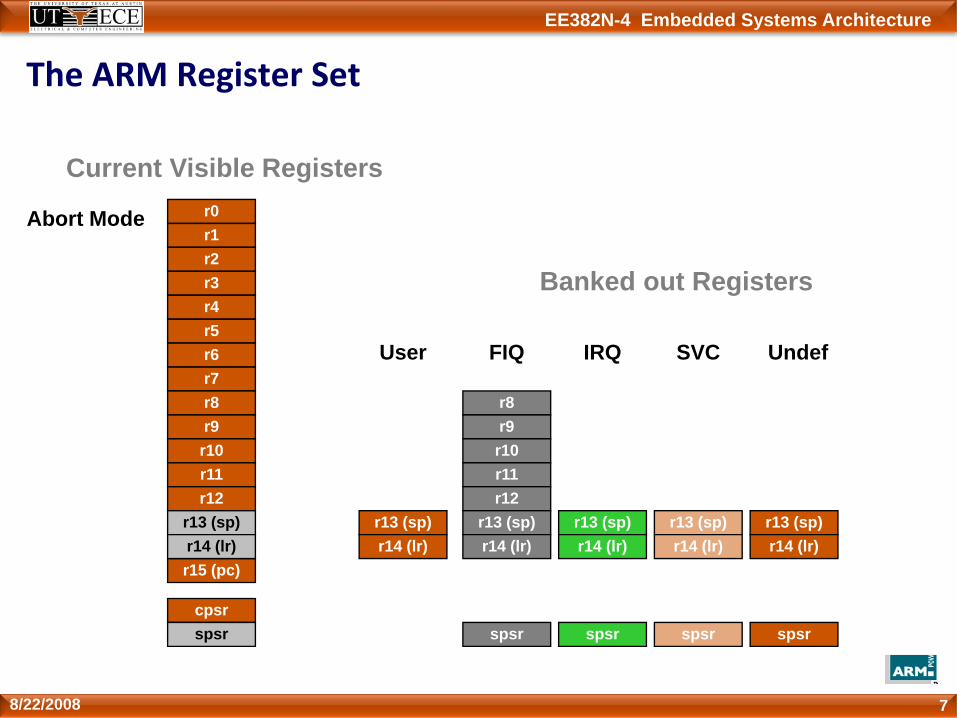
ARM has 37 registers in total, all of which are 32‐bits long.– 1 dedicated program counter– 1 dedicated current program status register– 5 dedicated saved program status registers– 30 general purpose registers
However these are arranged into several banks, with the accessible bank being governed by the processor mode. Each mode can access – a particular set of r0‐r12 registers– a particular r13 (the stack pointer) and r14 (link register)– r15 (the program counter)– cpsr (the current program status register)
And privileged modes can also access– a particular spsr (saved program status register)
68/22/2008
EE382N-4 Embedded Systems Architecture
r0r1r2r3r4r5r6r7r8r9r10r11r12
r13 (sp)r14 (lr)r15 (pc)
cpsr
r13 (sp)r14 (lr)
spsr
r13 (sp)r14 (lr)
spsr
r13 (sp)r14 (lr)
spsr
r13 (sp)r14 (lr)
spsr
r8r9r10r11r12
r13 (sp)r14 (lr)
spsr
FIQ IRQ SVC Undef Abort
User Mode r0r1r2r3r4r5r6r7r8r9r10r11r12
r13 (sp)r14 (lr)r15 (pc)
cpsr
r13 (sp)r14 (lr)
spsr
r13 (sp)r14 (lr)
spsr
r13 (sp)r14 (lr)
spsr
r13 (sp)r14 (lr)
spsr
r8r9r10r11r12
r13 (sp)r14 (lr)
spsr
Current Visible Registers
Banked out Registers
FIQ IRQ SVC Undef Abort
r0r1r2r3r4r5r6r7
r15 (pc)
cpsr
r13 (sp)r14 (lr)
spsr
r13 (sp)r14 (lr)
spsr
r13 (sp)r14 (lr)
spsr
r13 (sp)r14 (lr)
spsr
r8r9r10r11r12
r13 (sp)r14 (lr)
spsr
Current Visible Registers
Banked out Registers
User IRQ SVC Undef Abort
r8r9r10r11r12
r13 (sp)r14 (lr)
FIQ ModeIRQ Mode r0r1r2r3r4r5r6r7r8r9r10r11r12
r15 (pc)
cpsr
r13 (sp)r14 (lr)
spsr
r13 (sp)r14 (lr)
spsr
r13 (sp)r14 (lr)
spsr
r13 (sp)r14 (lr)
spsr
r8r9r10r11r12
r13 (sp)r14 (lr)
spsr
Current Visible Registers
Banked out Registers
User FIQ SVC Undef Abort
r13 (sp)r14 (lr)
Undef Mode r0r1r2r3r4r5r6r7r8r9r10r11r12
r15 (pc)
cpsr
r13 (sp)r14 (lr)
spsr
r13 (sp)r14 (lr)
spsr
r13 (sp)r14 (lr)
spsr
r13 (sp)r14 (lr)
spsr
r8r9r10r11r12
r13 (sp)r14 (lr)
spsr
Current Visible Registers
Banked out Registers
User FIQ IRQ SVC Abort
r13 (sp)r14 (lr)
SVC Mode r0r1r2r3r4r5r6r7r8r9r10r11r12
r15 (pc)
cpsr
r13 (sp)r14 (lr)
spsr
r13 (sp)r14 (lr)
spsr
r13 (sp)r14 (lr)
spsr
r13 (sp)r14 (lr)
spsr
r8r9r10r11r12
r13 (sp)r14 (lr)
spsr
Current Visible Registers
Banked out Registers
User FIQ IRQ Undef Abort
r13 (sp)r14 (lr)
Abort Mode r0r1r2r3r4r5r6r7r8r9r10r11r12
r15 (pc)
cpsr
r13 (sp)r14 (lr)
spsr
r13 (sp)r14 (lr)
spsr
r13 (sp)r14 (lr)
spsr
r13 (sp)r14 (lr)
spsr
r8r9r10r11r12
r13 (sp)r14 (lr)
spsr
Current Visible Registers
Banked out Registers
User FIQ IRQ SVC Undef
r13 (sp)r14 (lr)
The ARM Register Set
78/22/2008

EE382N-4 Embedded Systems Architecture
Register Organization Summary
88/22/2008
Usermoder0-r7,r15,andcpsr
r8r9r10r11r12
r13 (sp)r14 (lr)
spsr
FIQ
r8r9
r10r11r12
r13 (sp)r14 (lr)r15 (pc)
cpsr
r0r1r2r3r4r5r6r7
User
r13 (sp)r14 (lr)
spsr
IRQ
Usermoder0-r12,
r15,andcpsr
r13 (sp)r14 (lr)
spsr
Undef
Usermoder0-r12,
r15,andcpsr
r13 (sp)r14 (lr)
spsr
SVC
Usermoder0-r12,
r15,andcpsr
r13 (sp)r14 (lr)
spsr
Abort
Usermoder0-r12,
r15,andcpsr
Thumb stateLow registers
Thumb stateHigh registers
Note: System mode uses the User mode register set
EE382N-4 Embedded Systems Architecture
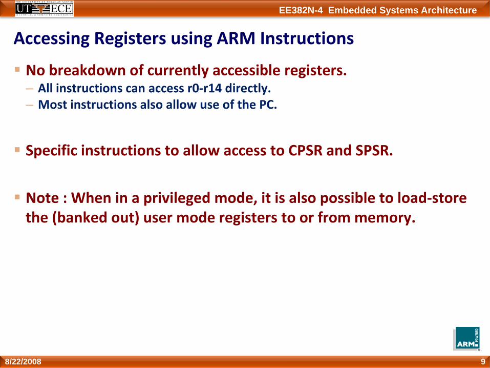
Accessing Registers using ARM Instructions
No breakdown of currently accessible registers.– All instructions can access r0‐r14 directly.– Most instructions also allow use of the PC.
Specific instructions to allow access to CPSR and SPSR.
Note : When in a privileged mode, it is also possible to load‐store the (banked out) user mode registers to or from memory.
98/22/2008

EE382N-4 Embedded Systems Architecture
The Program Status Registers (CPSR and SPSRs)
108/22/2008
Copies of the ALU status flags (latched if theinstruction has the "S" bit set).
N = Negative result from ALU flag.Z = Zero result from ALU flag.C = ALU operation Carried outV = ALU operation oVerflowed
* Interrupt Disable bits.I = 1, disables the IRQ.F = 1, disables the FIQ.
* T Bit (Architecture v4T only)T = 0, Processor in ARM stateT = 1, Processor in Thumb state
* Condition Code Flags
ModeN Z C V
2831 8 4 0
I F T
* Mode BitsM[4:0] define the processor mode.

EE382N-4 Embedded Systems Architecture
Logical Instruction Arithmetic Instruction
Flag
Negative No meaning Bit 31 of the result has been set(N=‘1’) Indicates a negative number in
signed operations
Zero Result is all zeroes Result of operation was zero(Z=‘1’)
Carry After Shift operation Result was greater than 32 bits(C=‘1’) ‘1’ was left in carry flag
oVerflow No meaning Result was greater than 31 bits(V=‘1’) Indicates a possible corruption of
the sign bit in signed numbers
Condition Flags
118/22/2008

EE382N-4 Embedded Systems Architecture
The Program Counter (R15)
When the processor is executing in ARM state:– All instructions are 32 bits in length– All instructions must be word aligned– Therefore the PC value is stored in bits [31:2] with bits [1:0] equal to zero (as instruction cannot be halfword or byte aligned).
R14 is used as the subroutine link register (LR) and stores the return address when Branch with Link operations are performed, calculated from the PC.
Thus to return from a linked branch:MOV r15,r14or
MOV pc,lr
128/22/2008

EE382N-4 Embedded Systems Architecture
Exception Handling and the Vector Table
When an exception occurs, the core:– Copies CPSR into SPSR_<mode>– Sets appropriate CPSR bits • If core implements ARM Architecture 4T and is currently in Thumb state, then– ARM state is entered.
• Mode field bits • Interrupt disable flags if appropriate.
– Maps in appropriate banked registers– Stores the “return address” in LR_<mode>– Sets PC to vector address
To return, exception handler needs to:– Restore CPSR from SPSR_<mode>– Restore PC from LR_<mode>
138/22/2008

EE382N-4 Embedded Systems Architecture
The Original Instruction Pipeline
The ARM uses a pipeline in order to increase the speed of the flow of instructions to the processor.– Allows several operations to be undertaken simultaneously, rather than serially.
Rather than pointing to the instruction being executed, the PC points to the instruction being fetched.
148/22/2008
FETCH
DECODE
EXECUTE
Instruction fetched from memory
Decoding of registers used in instruction
Register(s) read from Register BankShift and ALU operationWrite register(s) back to Register Bank
PC
PC - 4
PC - 8

EE382N-4 Embedded Systems Architecture
Pipeline changes for ARM9TDMI
InstructionFetch Shift + ALU Memory
AccessRegWriteReg
ReadRegDecode
FETCH DECODE EXECUTE MEMORY WRITE
ARM9TDMI
ARM or ThumbInst Decode
Reg Select
RegRead Shift ALU Reg
WriteThumb→ARMdecompress
ARM decodeInstructionFetch
FETCH DECODE EXECUTE
ARM7TDMI

EE382N-4 Embedded Systems Architecture
Pipeline changes for ARM10 vs. ARM11 Pipelines
ARM11
Fetch1
Fetch2 Decode Issue
Shift ALU Saturate
Writeback
MAC1
MAC2
MAC3
AddressDataCache1
DataCache2
Shift + ALU MemoryAccess Reg
Write
FETCH DECODE EXECUTE MEMORY WRITE
Reg Read
Multiply
BranchPrediction
InstructionFetch
ISSUE
ARM or ThumbInstructionDecode Multiply
Add
ARM10

EE382N-4 Embedded Systems Architecture
ARM Instruction Set Format
178/22/2008
31
30
29
28
27
26
25
24
23
22
21
20
19
18
17
16
15
14
13
12
11
10 9 8 7 6 5 4 3 2 1 0 Instruction Type
Condition 0 0 I OPCODE S Rn Rs OPERAND‐2 Data processing
Condition 0 0 0 0 0 0 A S Rd Rn Rs 1 0 0 1 Rm Multiply
Condition 0 0 0 0 1 U A S Rd HIGH Rd LOW Rs 1 0 0 1 Rm Long Multiply
Condition 0 0 0 1 0 B 0 0 Rn Rd 0 0 0 0 1 0 0 1 Rm Swap
Condition 0 1 I P U B W L Rn Rd OFFSET Load/Store ‐ Byte/Word
Condition 1 0 0 P U B W L Rn REGISTER LIST Load/Store Multiple
Condition 0 0 0 P U 1 W L Rn Rd OFFSET 1 1 S H 1 OFFSET 2 Halfword Transfer Imm Off
Condition 0 0 0 P U 0 W L Rn Rd 0 0 0 0 1 S H 1 Rm Halfword Transfer Reg Off
Condition 1 0 1 L BRANCH OFFSET Branch
Condition 0 0 0 1 0 0 1 0 1 1 1 1 1 1 1 1 1 1 1 1 0 0 0 1 Rn Branch Exchange
Condition 1 1 0 P U N W L Rn CRd CPNum OFFSET COPROCESSOR DATA XFER
Condition 1 1 1 0 Op‐1 CRn CRd CPNum OP‐2 0 CRm COPROCESSOR DATA OP
Condition OP‐1 L CRn Rd CPNum OP‐2 1 CRm COPROCESSOR REG XFER
Condition 1 1 1 1 SWI NUMBER Software Interrupt
EE382N-4 Embedded Systems Architecture
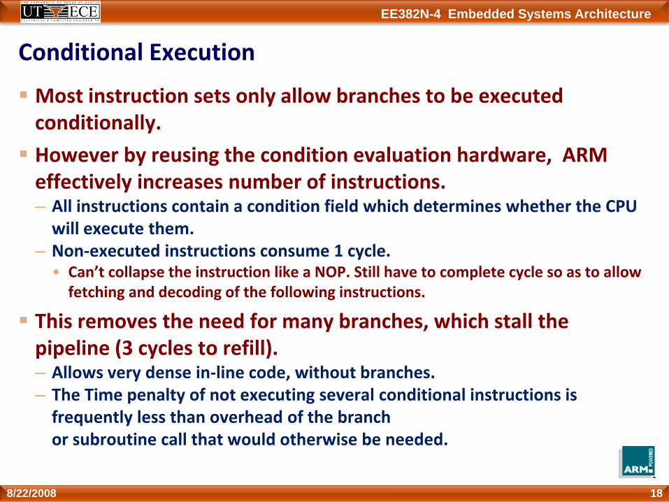
Conditional Execution
Most instruction sets only allow branches to be executed conditionally.
However by reusing the condition evaluation hardware, ARM effectively increases number of instructions.– All instructions contain a condition field which determines whether the CPU will execute them.
– Non‐executed instructions consume 1 cycle.• Can’t collapse the instruction like a NOP. Still have to complete cycle so as to allow fetching and decoding of the following instructions.
This removes the need for many branches, which stall the pipeline (3 cycles to refill).– Allows very dense in‐line code, without branches.– The Time penalty of not executing several conditional instructions is frequently less than overhead of the branch or subroutine call that would otherwise be needed.
188/22/2008

EE382N-4 Embedded Systems Architecture
The Condition Field
198/22/2008
1001 = LS - C clear or Z (set unsigned lower or same)
1010 = GE - N set and V set, or N clear and V clear (>or =)
1011 = LT - N set and V clear, or N clear and V set (>)
1100 = GT - Z clear, and either N set and V set, or N clear and V set (>)
1101 = LE - Z set, or N set and V clear,or N clear and V set (<, or =)
1110 = AL - always
1111 = NV - reserved.
0000 = EQ - Z set (equal)
0001 = NE - Z clear (not equal)
0010 = HS / CS - C set (unsigned higher or same)
0011 = LO / CC - C clear (unsigned lower)
0100 = MI -N set (negative)
0101 = PL - N clear (positive or zero)
0110 = VS - V set (overflow)
0111 = VC - V clear (no overflow)
1000 = HI - C set and Z clear (unsigned higher)
31
30
29
28
27
26
25
24
23
22
21
20
19
18
17
16
15
14
13
12
11
10 9 8 7 6 5 4 3 2 1 0 Instruction Type
Condition 0 0 I OPCODE S Rn Rs OPERAND‐2 Data processing

EE382N-4 Embedded Systems Architecture
Using and updating the Condition Field
To execute an instruction conditionally, simply postfix it with the appropriate condition:– For example an add instruction takes the form:
• ADD r0,r1,r2 ; r0 = r1 + r2 (ADDAL)– To execute this only if the zero flag is set:
• ADDEQ r0,r1,r2 ; If zero flag set then…; ... r0 = r1 + r2
By default, data processing operations do not affect the condition flags (apart from the comparisons where this is the only effect). To cause the condition flags to be updated, the S bit of the instruction needs to be set by postfixing the instruction (and any condition code) with an “S”.– For example to add two numbers and set the condition flags:
• ADDS r0,r1,r2 ; r0 = r1 + r2 ; ... and set flags
208/22/2008

EE382N-4 Embedded Systems Architecture
Conditional Execution and FlagsARM instructions can be made to execute conditionally by postfixing them with the appropriate condition code field.– This improves code density and performance by reducing the number of forward branch instructions.CMP r3,#0 CMP r3,#0BEQ skip ADDNE r0,r1,r2ADD r0,r1,r2
skip
By default, data processing instructions do not affect the condition code flags but the flags can be optionally set by using “S”. CMP does not need “S”.loop…SUBS r1,r1,#1BNE loop
218/22/2008
if Z flag clear then branch
decrement r1 and set flags

EE382N-4 Embedded Systems Architecture
Branch instructions (1)
228/22/2008
Branch : B{<cond>} labelBranch with Link : BL{<cond>} sub_routine_label
The offset for branch instructions is calculated by the assembler:– By taking the difference between the branch instruction and the target address minus 8 (to allow for the pipeline).
– This gives a 26 bit offset which is right shifted 2 bits (as the bottom two bits are always zero as instructions are word – aligned) and stored into the instruction encoding.
– This gives a range of ± 32 Mbytes.
Condition field
Link bit 0 = Branch1 = Branch with link
31
30
29
28
27
26
25
24
23
22
21
20
19
18
17
16
15
14
13
12
11
10 9 8 7 6 5 4 3 2 1 0
Condition 1 0 1 L BRANCH OFFSET

EE382N-4 Embedded Systems Architecture
Branch instructions (2)
When executing the instruction, the processor:– shifts the offset left two bits, sign extends it to 32 bits, and adds it to PC.
Execution then continues from the new PC, once the pipeline has been refilled.
The "Branch with link" instruction implements a subroutine call by writing PC‐4 into the LR of the current bank. – i.e. the address of the next instruction following the branch with link (allowing for the pipeline).
To return from subroutine, simply need to restore the PC from the LR:– MOV pc, lr– Again, pipeline has to refill before execution continues.
238/22/2008

EE382N-4 Embedded Systems Architecture
Branch instructions (3)
The "Branch" instruction does not affect LR.
Note: Architecture 4T offers a further ARM branch instruction, BX– See Thumb Instruction Set Module for details.
BL <subroutine>– Stores return address in LR– Returning implemented by restoring the PC from LR– For non‐leaf functions, LR will have to be stacked
248/22/2008
STMFD sp!,{regs,lr}:BL func2:LDMFD sp!,{regs,pc}
func1 func2
::BL func1::
:::::MOV pc, lr
EE382N-4 Embedded Systems Architecture
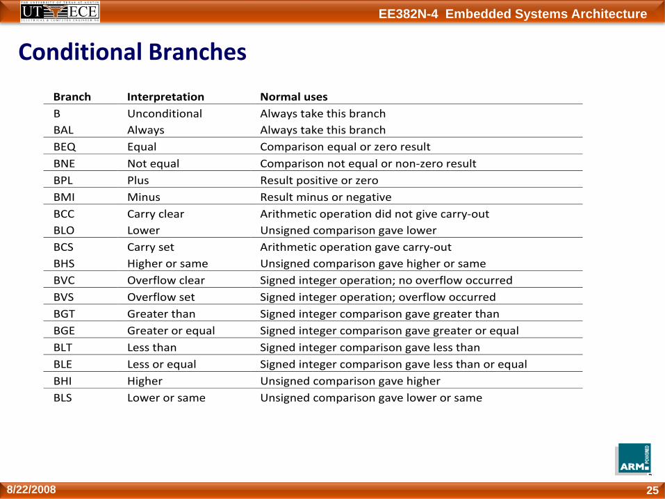
Conditional Branches
258/22/2008
Branch Interpretation Normal uses B BAL
Unconditional Always
Always take this branch Always take this branch
BEQ Equal Comparison equal or zero result BNE Not equal Comparison not equal or non‐zero result BPL Plus Result positive or zero BMI Minus Result minus or negative BCC BLO
Carry clear Lower
Arithmetic operation did not give carry‐out Unsigned comparison gave lower
BCS BHS
Carry set Higher or same
Arithmetic operation gave carry‐out Unsigned comparison gave higher or same
BVC Overflow clear Signed integer operation; no overflow occurred BVS Overflow set Signed integer operation; overflow occurred BGT Greater than Signed integer comparison gave greater than BGE Greater or equal Signed integer comparison gave greater or equal BLT Less than Signed integer comparison gave less than BLE Less or equal Signed integer comparison gave less than or equal BHI Higher Unsigned comparison gave higher BLS Lower or same Unsigned comparison gave lower or same

EE382N-4 Embedded Systems Architecture
Data processing Instructions
Largest family of ARM instructions, all sharing the same instruction format.
Contains:– Arithmetic operations– Comparisons (no results ‐ just set condition codes) – Logical operations– Data movement between registers
Remember, this is a load / store architecture– These instruction only work on registers, NOT memory.
They each perform a specific operation on one or two operands.– First operand always a register ‐ Rn– Second operand sent to the ALU via barrel shifter.
We will examine the barrel shifter shortly.
268/22/2008

EE382N-4 Embedded Systems Architecture
Arithmetic Operations
Operations are:– ADD operand1 + operand2 ; Add– ADC operand1 + operand2 + carry ; Add with carry– SUB operand1 ‐ operand2 ; Subtract– SBC operand1 ‐ operand2 + carry ‐1 ; Subtract with carry– RSB operand2 ‐ operand1 ; Reverse subtract– RSC operand2 ‐ operand1 + carry ‐ 1 ; Reverse subtract with carry
Syntax:– <Operation>{<cond>}{S} Rd, Rn, Operand2
Examples– ADD r0, r1, r2– SUBGT r3, r3, #1– RSBLES r4, r5, #5
278/22/2008
EE382N-4 Embedded Systems Architecture
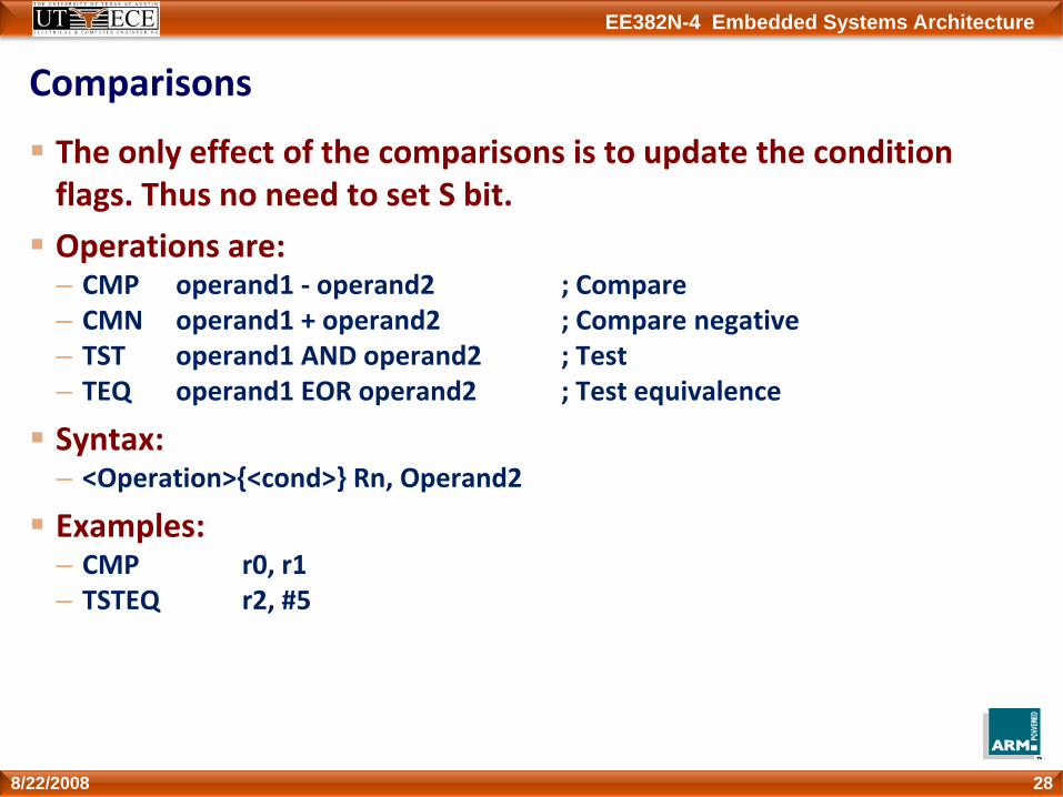
Comparisons
The only effect of the comparisons is to update the condition flags. Thus no need to set S bit.
Operations are:– CMP operand1 ‐ operand2 ; Compare– CMN operand1 + operand2 ; Compare negative– TST operand1 AND operand2 ; Test– TEQ operand1 EOR operand2 ; Test equivalence
Syntax:– <Operation>{<cond>} Rn, Operand2
Examples:– CMP r0, r1– TSTEQ r2, #5
288/22/2008

EE382N-4 Embedded Systems Architecture
Logical Operations
Operations are:AND operand1 AND operand2EOR operand1 EOR operand2ORR operand1 OR operand2ORN operand1 NOR operand2BIC operand1 AND NOT operand2 [ie bit clear]
Syntax:– <Operation>{<cond>}{S} Rd, Rn, Operand2
Examples:AND r0, r1, r2BICEQ r2, r3, #7EORS r1,r3,r0
298/22/2008

EE382N-4 Embedded Systems Architecture
Data Movement
Operations are:MOV operand2MVN NOT operand2
Note that these make no use of operand1.
Syntax:– <Operation>{<cond>}{S} Rd, Operand2
Examples:MOV r0, r1MOVS r2, #10MVNEQ r1,#0
308/22/2008

EE382N-4 Embedded Systems Architecture
The Barrel Shifter
The ARM doesn’t have actual shift instructions.
Instead it has a barrel shifter which provides a mechanism to carry out shifts as part of other instructions.
So what operations does the barrel shifter support?
318/22/2008

EE382N-4 Embedded Systems Architecture
Barrel Shifter ‐ Left Shift
Shifts left by the specified amount (multiplies by powers of two) e.g.
LSL #5 => multiply by 32
328/22/2008
Logical Shift Left (LSL)
DestinationCF 0

EE382N-4 Embedded Systems Architecture
Barrel Shifter ‐ Right Shifts
338/22/2008
Logical Shift Right (LSR) Shifts right by the specified amount (divides by powers of two) e.g.
LSR #5 = divide by 32
Arithmetic Shift Right (ASR) Shifts right (divides by powers of two) and preserves the sign bit, for 2's complement operations. e.g.
ASR #5 = divide by 32
Destination CF
Destination CF
Logical Shift Right
Arithmetic Shift Right
...0
Sign bit shifted in
zero shifted in

EE382N-4 Embedded Systems Architecture
Barrel Shifter ‐ Rotations
348/22/2008
Rotate Right (ROR)
Similar to an ASR but the bits wrap around as they leave the LSB and appear as the MSB.
e.g. ROR #5
Note the last bit rotated is also used as the Carry Out.
Rotate Right Extended (RRX)
This operation uses the CPSR C flag as a 33rd bit.
Rotates right by 1 bit. Encoded as ROR #0
Destination CF
Rotate Right
Destination CF
Rotate Right through Carry

EE382N-4 Embedded Systems Architecture
Using the Barrel Shifter: The Second Operand
358/22/2008
Register, optionally with shift operation applied.Shift value can be either be:5 bit unsigned integerSpecified in bottom byte of another register.
* Immediate value
8 bit number
Can be rotated right through an even number of positions.
Assembler will calculate rotate for you from constant.
Operand 1
Result
ALU
Barrel Shifter
Operand 2

EE382N-4 Embedded Systems Architecture
Second Operand : Shifted Register
The amount by which the register is to be shifted is contained in either: – the immediate 5‐bit field in the instruction • NO OVERHEAD • Shift is done for free ‐ executes in single cycle.
– the bottom byte of a register (not PC)• Then takes extra cycle to execute• ARM doesn’t have enough read ports to read 3 registers at once.• Then same as on other processors where shift isseparate instruction.
If no shift is specified then a default shift is applied: LSL #0– i.e. barrel shifter has no effect on value in register.
368/22/2008

EE382N-4 Embedded Systems Architecture
Second Operand: Using a Shifted Register
Using a multiplication instruction to multiply by a constant means first loading the constant into a register and then waiting a number of internal cycles for the instruction to complete.
A more optimum solution can often be found by using some combination of MOVs, ADDs, SUBs and RSBs with shifts.– Multiplications by a constant equal to a ((power of 2) ± 1) can be done in one cycle.
MOV R2, R0, LSL #2 ; Shift R0 left by 2, write to R2, (R2=R0x4)ADD R9, R5, R5, LSL #3 ; R9 = R5 + R5 x 8 or R9 = R5 x 9RSB R9, R5, R5, LSL #3 ; R9 = R5 x 8 ‐ R5 or R9 = R5 x 7SUB R10, R9, R8, LSR #4 ; R10 = R9 ‐ R8 / 16MOV R12, R4, ROR R3 ; R12 = R4 rotated right by value of R3
378/22/2008
EE382N-4 Embedded Systems Architecture
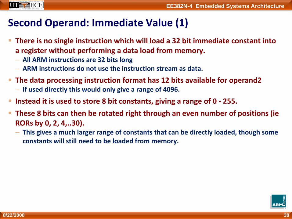
Second Operand: Immediate Value (1)
There is no single instruction which will load a 32 bit immediate constant into a register without performing a data load from memory.– All ARM instructions are 32 bits long– ARM instructions do not use the instruction stream as data.
The data processing instruction format has 12 bits available for operand2– If used directly this would only give a range of 4096.
Instead it is used to store 8 bit constants, giving a range of 0 ‐ 255.
These 8 bits can then be rotated right through an even number of positions (ie RORs by 0, 2, 4,..30).– This gives a much larger range of constants that can be directly loaded, though some constants will still need to be loaded from memory.
388/22/2008

EE382N-4 Embedded Systems Architecture
Second Operand: Immediate Value (2)
This gives us:– 0 ‐ 255 [0 ‐ 0xff]– 256,260,264,..,1020 [0x100‐0x3fc, step 4, 0x40‐0xff ror 30]– 1024,1040,1056,..,4080 [0x400‐0xff0, step 16, 0x40‐0xff ror 28]– 4096,4160, 4224,..,16320 [0x1000‐0x3fc0, step 64, 0x40‐0xff ror 26]
These can be loaded using, for example:– MOV r0, #0x40, 26 ; => MOV r0, #0x1000 (ie 4096)
To make this easier, the assembler will convert to this form for us if simply given the required constant:– MOV r0, #4096 ; => MOV r0, #0x1000 (ie 0x40 ror 26)
The bitwise complements can also be formed using MVN:– MOV r0, #0xFFFFFFFF ; assembles to MVN r0, #0
If the required constant cannot be generated, an error will be reported.
398/22/2008

EE382N-4 Embedded Systems Architecture
Loading full 32 bit constants
Although the MOV/MVN mechanism will load a large range of constants into a register, sometimes this mechanism will not generate the required constant.
Therefore, the assembler also provides a method which will load ANY 32 bit constant:– LDR rd,=numeric constant
If the constant can be constructed using either a MOV or MVN then this will be the instruction actually generated.
Otherwise, the assembler will produce an LDR instruction with a PC‐relative address to read the constant from a literal pool.LDR r0,=0x42 ; generates MOV r0,#0x42LDR r0,=0x55555555 ; generate LDR r0,[pc, offset to lit pool]
::
DCD 0x55555555
As this mechanism will always generate the best instruction for a given case, it is the recommended way of loading constants.
408/22/2008

EE382N-4 Embedded Systems Architecture
Multiplication Instructions
The Basic ARM provides two multiplication instructions.
Multiply– MUL{<cond>}{S} Rd, Rm, Rs ; Rd = Rm * Rs
Multiply Accumulate ‐ does addition for free– MLA{<cond>}{S} Rd, Rm, Rs,Rn ; Rd = (Rm * Rs) + Rn
Restrictions on use:– Rd and Rm cannot be the same register• Can be avoided by swapping Rm and Rs around. This works because multiplication is commutative.
– Cannot use PC.
These will be picked up by the assembler if overlooked.
Operands can be considered signed or unsigned– Up to user to interpret correctly.
418/22/2008

EE382N-4 Embedded Systems Architecture
Multiplication Implementation
The ARM makes use of Booth’s Algorithm to perform integer multiplication.
On non‐M ARMs this operates on 2 bits of Rs at a time.– For each pair of bits this takes 1 cycle (plus 1 cycle to start with).– However when there are no more 1’s left in Rs, the multiplication will early‐terminate.
Example: Multiply 18 and ‐1 : Rd = Rm * Rs
Note: Compiler does not use early termination criteria to decide on which order to place operands.
428/22/2008
0 0 0 0 0 0 1 00 0 0 10 0 0 00 0 0 00 0 0 0 0 0 0 0 0 0 0 0
1 1 1 1 1 1 1 11 1 1 11 1 1 11 1 1 11 1 1 1 1 1 1 1 1 1 1 1
Rm
Rs
17 cycles
Rs
Rm
4 cycles
18
‐1
18
‐1
EE382N-4 Embedded Systems Architecture
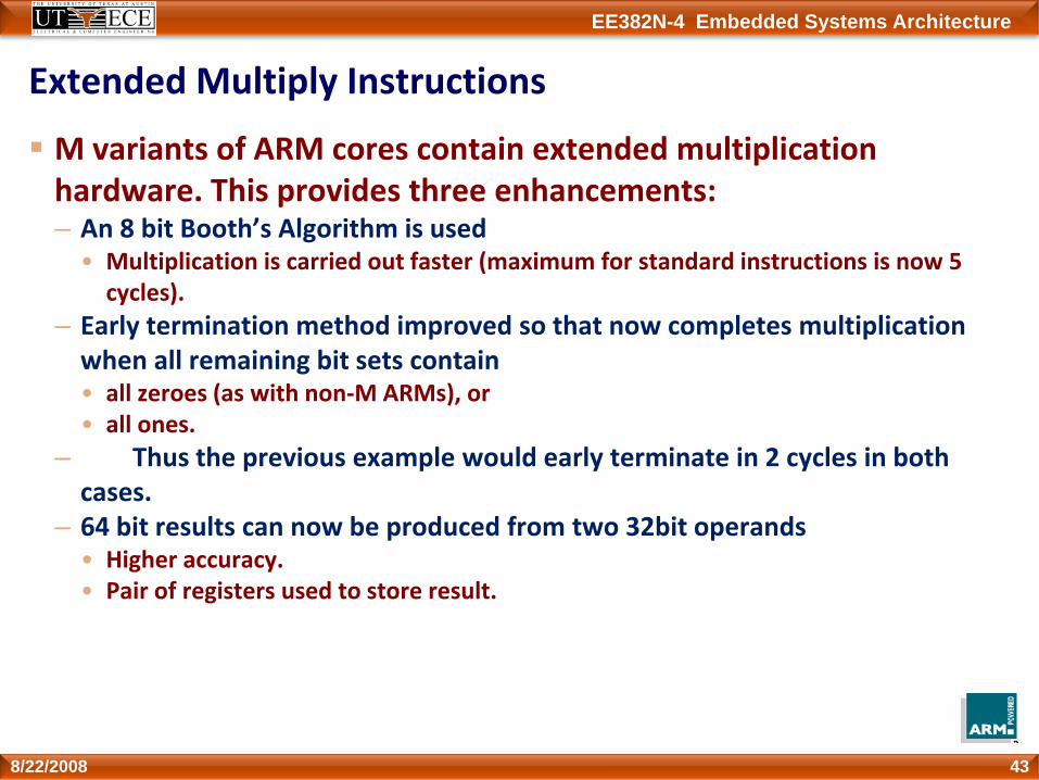
Extended Multiply Instructions
M variants of ARM cores contain extended multiplication hardware. This provides three enhancements:– An 8 bit Booth’s Algorithm is used• Multiplication is carried out faster (maximum for standard instructions is now 5 cycles).
– Early termination method improved so that now completes multiplication when all remaining bit sets contain • all zeroes (as with non‐M ARMs), or• all ones.
– Thus the previous example would early terminate in 2 cycles in both cases.
– 64 bit results can now be produced from two 32bit operands• Higher accuracy.• Pair of registers used to store result.
438/22/2008

EE382N-4 Embedded Systems Architecture
Multiply‐Long & Multiply‐Accumulate Long
Instructions are– MULL which gives RdHi,RdLo:=Rm*Rs – MLAL which gives RdHi,RdLo:=(Rm*Rs)+RdHi,RdLo
However the full 64 bit of the result now matter (lower precision multiply instructions simply throws top 32bits away)– Need to specify whether operands are signed or unsigned
Therefore syntax of new instructions are:– UMULL{<cond>}{S} RdLo,RdHi,Rm,Rs– UMLAL{<cond>}{S} RdLo,RdHi,Rm,Rs– SMULL{<cond>}{S} RdLo, RdHi, Rm, Rs– SMLAL{<cond>}{S} RdLo, RdHi, Rm, Rs
Not generated by the compiler.
Warning : Unpredictable on non‐M ARMs.
448/22/2008

EE382N-4 Embedded Systems Architecture
Load / Store Instructions
The ARM is a Load / Store Architecture:– Does not support memory to memory data processing operations.– Must move data values into registers before using them.
This might sound inefficient, but in practice it isn’t:– Load data values from memory into registers.– Process data in registers using a number of data processing instructions which are not slowed down by memory access.
– Store results from registers out to memory.
The ARM has three sets of instructions which interact with main memory. These are:– Single register data transfer (LDR / STR).– Block data transfer (LDM/STM).– Single Data Swap (SWP).
458/22/2008

EE382N-4 Embedded Systems Architecture
Single register data transfer
The basic load and store instructions are:– Load and Store Word or Byte• LDR / STR / LDRB / STRB
ARM Architecture Version 4 also adds support for Halfwords and signed data.– Load and Store Halfword• LDRH / STRH
– Load Signed Byte or Halfword ‐ load value and sign extend it to 32 bits.• LDRSB / LDRSH
All of these instructions can be conditionally executed by inserting the appropriate condition code after STR / LDR.– e.g. LDREQB
Syntax:– <LDR|STR>{<cond>}{<size>} Rd, <address>
468/22/2008

EE382N-4 Embedded Systems Architecture
Load and Store Word or Byte: Base Register
The memory location to be accessed is held in a base register
STR r0, [r1] ; Store contents of r0 to location pointed to; by contents of r1.
LDR r2, [r1] ; Load r2 with contents of memory location; pointed to by contents of r1.
478/22/2008
r1
0x200Base
Register
Memory
0x50x200
r0
0x5SourceRegisterfor STR
r2
0x5DestinationRegisterfor LDR

EE382N-4 Embedded Systems Architecture
Load/Store Word or Byte: Offsets from the Base Register
As well as accessing the actual location contained in the base register, these instructions can access a location offset from the base register pointer.
This offset can be– An unsigned 12bit immediate value (ie 0 ‐ 4095 bytes).– A register, optionally shifted by an immediate value
This can be either added or subtracted from the base register:– Prefix the offset value or register with ‘+’ (default) or ‘‐’.
This offset can be applied:– before the transfer is made: Pre‐indexed addressing• optionally auto‐incrementing the base register, by postfixing the instruction with an ‘!’.
– after the transfer is made: Post‐indexed addressing• causing the base register to be auto‐incremented.
488/22/2008

EE382N-4 Embedded Systems Architecture
Load/Store Word or Byte: Pre‐indexed Addressing
Example: STR r0, [r1,#12]
– To store to location 0x1f4 instead use: STR r0, [r1,#‐12]– To auto‐increment base pointer to 0x20c use: STR r0, [r1, #12]!– If r2 contains 3, access 0x20c by multiplying this by 4:• STR r0, [r1, r2, LSL #2]
498/22/2008
r1
0x200Base
Register
Memory
0x5
0x200
r0
0x5SourceRegisterfor STR
Offset
12 0x20c
EE382N-4 Embedded Systems Architecture
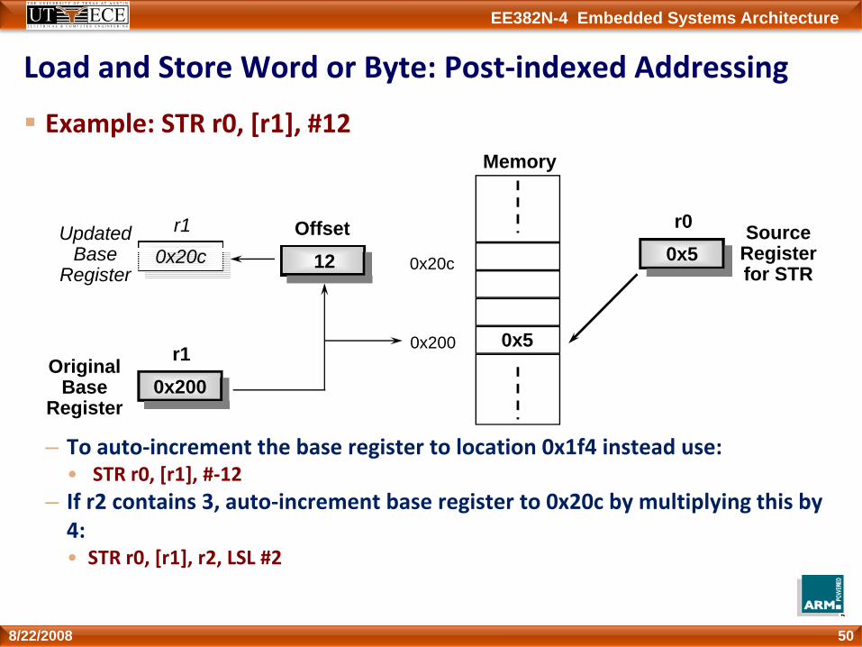
Load and Store Word or Byte: Post‐indexed Addressing
Example: STR r0, [r1], #12
– To auto‐increment the base register to location 0x1f4 instead use:• STR r0, [r1], #‐12
– If r2 contains 3, auto‐increment base register to 0x20c by multiplying this by 4:• STR r0, [r1], r2, LSL #2
508/22/2008
r10x200
OriginalBase
Register
Memory
0x50x200
r00x5
SourceRegisterfor STR
Offset12 0x20c
r10x20c
UpdatedBase
Register

EE382N-4 Embedded Systems Architecture
Load and Stores with User Mode Privilege
When using post‐indexed addressing, there is a further form of Load/Store Word/Byte:– <LDR|STR>{<cond>}{B}T Rd, <post_indexed_address>
When used in a privileged mode, this does the load/store with user mode privilege.– Normally used by an exception handler that is emulating a memory access instruction that would normally execute in user mode.
518/22/2008

EE382N-4 Embedded Systems Architecture
Example Usage of Addressing Modes
Imagine an array, the first element of which is pointed to by the contents of r0.
If we want to access a particular element,then we can use pre‐indexed addressing:– r1 is element we want.– LDR r2, [r0, r1, LSL #2]
If we want to step through everyelement of the array, for instanceto produce sum of elements in thearray, then we can use post‐indexed addressing within a loop:– r1 is address of current element (initially equal to r0).– LDR r2, [r1], #4
Use a further register to store the address of final element,so that the loop can be correctly terminated.
528/22/2008
0123
element
048
12
Memory Offset
r0
Pointer to start of array

EE382N-4 Embedded Systems Architecture
Offsets for Halfword and Signed Halfword / Byte Access
The Load and Store Halfword and Load Signed Byte or Halfword instructions can make use of pre‐ and post‐indexed addressing in much the same way as the basic load and store instructions.
However the actual offset formats are more constrained:– The immediate value is limited to 8 bits (rather than 12 bits) giving an offset of 0‐255 bytes.
– The register form cannot have a shift applied to it.
538/22/2008

EE382N-4 Embedded Systems Architecture
Effect of endianess
The ARM can be set up to access its data in either little or big endian format.
Little endian:– Least significant byte of a word is stored in bits 0‐7 of an addressed word.
Big endian:– Least significant byte of a word is stored in bits 24‐31 of an addressed word.
This has no real relevance unless data is stored as words and then accessed in smaller sized quantities (halfwords or bytes).– Which byte / halfword is accessed will depend on the endianess of the system involved.
548/22/2008

EE382N-4 Embedded Systems Architecture
YA Endianess Example
558/22/2008
Big-endianLittle-endian
r1 = 0x100
r0 = 0x1122334431 24 23 16 15 8 7 0
11 22 33 44
31 24 23 16 15 8 7 0
11 22 33 44
31 24 23 16 15 8 7 0
44 33 22 11
31 24 23 16 15 8 7 0
00 00 00 44
31 24 23 16 15 8 7 0
00 00 00 11
r2 = 0x44 r2 = 0x11
STR r0, [r1]
LDRB r2, [r1]
r1 = 0x100Memory

EE382N-4 Embedded Systems Architecture
Block Data Transfer (1)
The Load and Store Multiple instructions (LDM / STM) allow betweeen 1 and 16 registers to be transferred to or from memory.
The transferred registers can be either:– Any subset of the current bank of registers (default).– Any subset of the user mode bank of registers when in a priviledged mode (postfix instruction with a ‘^’).
568/22/2008
Cond 1 0 0 P U S W L Rn Register list
Condition field Base registerLoad/Store bit0 = Store to memory1 = Load from memoryWrite- back bit0 = no write-back1 = write address into basePSR and force user bit0 = don’t load PSR or force user mode1 = load PSR or force user mode
Up/Down bit0 = Down; subtract offset from base1 = Up ; add offset to base
Pre/Post indexing bit0 = Post; add offset after transfer,1 = Pre ; add offset before transfer
2831 22 16 023 21 1527 20 1924
Each bit corresponds to a particular register. For example:• Bit 0 set causes r0 to be transferred.• Bit 0 unset causes r0 not to be transferred.At least one register must be transferred as the list cannot be empty.

EE382N-4 Embedded Systems Architecture
Block Data Transfer (2)
Base register used to determine where memory access should occur.– 4 different addressing modes allow increment and decrement inclusive or exclusive of the base register location.
– Base register can be optionally updated following the transfer (by appending it with an ‘!’.
– Lowest register number is always transferred to/from lowest memory location accessed.
These instructions are very efficient for– Saving and restoring context• For this useful to view memory as a stack.
– Moving large blocks of data around memory• For this useful to directly represent functionality of the instructions.
578/22/2008
EE382N-4 Embedded Systems Architecture
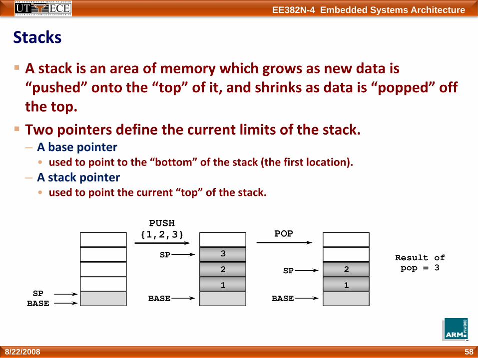
Stacks
A stack is an area of memory which grows as new data is “pushed” onto the “top” of it, and shrinks as data is “popped” off the top.
Two pointers define the current limits of the stack.– A base pointer • used to point to the “bottom” of the stack (the first location).
– A stack pointer• used to point the current “top” of the stack.
588/22/2008
SPBASE
PUSH {1,2,3}
1
2
3
BASE
SP
POP
1
2Result of pop = 3
BASE
SP

EE382N-4 Embedded Systems Architecture
Stack Operation
Traditionally, a stack grows down in memory, with the last “pushed” value at the lowest address. The ARM also supports ascending stacks, where the stack structure grows up through memory.
The value of the stack pointer can either:– Point to the last occupied address (Full stack)
• and so needs pre‐decrementing (ie before the push)– Point to the next occupied address (Empty stack)
• and so needs post‐decrementing (ie after the push)
The stack type to be used is given by the postfix to the instruction:– STMFD / LDMFD : Full Descending stack– STMFA / LDMFA : Full Ascending stack.– STMED / LDMED : Empty Descending stack– STMEA / LDMEA : Empty Ascending stack
Note: ARM Compiler will always use a Full descending stack.
598/22/2008

EE382N-4 Embedded Systems Architecture
Stack Examples
608/22/2008
STMFD sp!,{r0,r1,r3-r5}
r5r4r3r1r0SP
Old SP
STMED sp!,{r0,r1,r3-r5}
r5r4r3r1r0
SP
Old SP
r5r4r3r1r0
STMFA sp!,{r0,r1,r3-r5}
SP
Old SP 0x400
0x418
0x3e8
STMEA sp!,{r0,r1,r3-r5}
r5r4r3r1r0
SP
Old SP

EE382N-4 Embedded Systems Architecture
Stacks and Subroutines
One use of stacks is to create temporary register workspace for subroutines. Any registers that are needed can be pushed onto the stack at the start of the subroutine and popped off again at the end so as to restore them before return to the caller :
STMFD sp!,{r0-r12, lr} ; stack all registers........ ; and the return address........LDMFD sp!,{r0-r12, pc} ; load all the registers
; and return automatically
See the chapter on the ARM Procedure Call Standard in the SDT Reference Manual for further details of register usage within subroutines.
If the pop instruction also had the ‘S’ bit set (using ‘^’) then the transfer of the PC when in a privileged mode would also cause the SPSR to be copied into the CPSR (see exception handling module).
618/22/2008

EE382N-4 Embedded Systems Architecture
Direct functionality of Block Data Transfer
When LDM / STM are not being used to implement stacks, it is clearer to specify exactly what functionality of the instruction is:– i.e. specify whether to increment / decrement the base pointer, before or after the memory access.
In order to do this, LDM / STM support a further syntax in addition to the stack one: – STMIA / LDMIA : Increment After– STMIB / LDMIB : Increment Before– STMDA / LDMDA : Decrement After– STMDB / LDMDB : Decrement Before
628/22/2008

EE382N-4 Embedded Systems Architecture
Example: Block Copy
Copy a block of memory, which is an exact multiple of 12 words long from the location pointed to by r12 to the location pointed to by r13. r14 points to the end of block to be copied.
; r12 points to the start of the source data
; r14 points to the end of the source data
; r13 points to the start of the destination data
loop LDMIA r12!, {r0-r11} ; load 48 bytes
STMIA r13!, {r0-r11} ; and store them
CMP r12, r14 ; check for the end
BNE loop ; and loop until done
– This loop transfers 48 bytes in 31 cycles– Over 50 Mbytes/sec at 33 MHz
638/22/2008
r13
r14
r12
Increasing Memory

EE382N-4 Embedded Systems Architecture
Swap and Swap Byte Instructions
Atomic operation of a memory read followed by a memory write which moves byte or word quantities between registers and memory.
Syntax:– SWP{<cond>}{B} Rd, Rm, [Rn]
To implement an actual swap of contents make Rd = Rm.
The compiler cannot produce this instruction.
648/22/2008
Rm Rd
Rn
32
1temp
Memory
EE382N-4 Embedded Systems Architecture
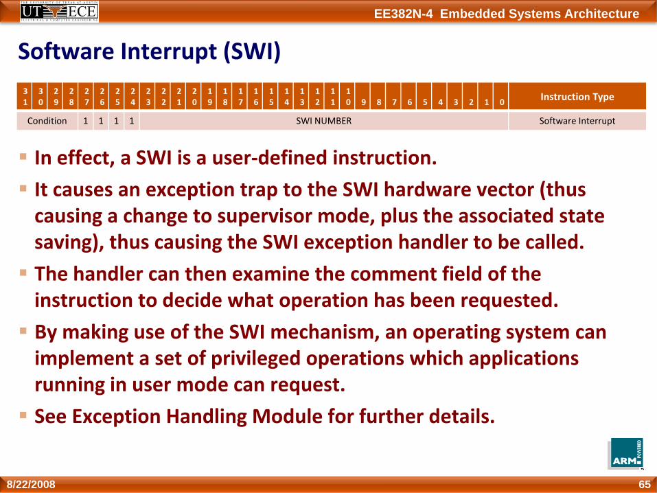
Software Interrupt (SWI)
In effect, a SWI is a user‐defined instruction.
It causes an exception trap to the SWI hardware vector (thus causing a change to supervisor mode, plus the associated state saving), thus causing the SWI exception handler to be called.
The handler can then examine the comment field of the instruction to decide what operation has been requested.
By making use of the SWI mechanism, an operating system can implement a set of privileged operations which applications running in user mode can request.
See Exception Handling Module for further details.
658/22/2008
31
30
29
28
27
26
25
24
23
22
21
20
19
18
17
16
15
14
13
12
11
10 9 8 7 6 5 4 3 2 1 0 Instruction Type
Condition 1 1 1 1 SWI NUMBER Software Interrupt

EE382N-4 Embedded Systems Architecture
Backup
8/22/2008

EE382N-4 Embedded Systems Architecture
Assembler: Pseudo‐ops
AREA ‐> chunks of data ($data) or code ($code)
ADR ‐> load address into a registerADR R0, BUFFER
ALIGN ‐> adjust location counter to word boundary usually after a storage directive
END ‐> no more to assemble
678/22/2008

EE382N-4 Embedded Systems Architecture
Assembler: Pseudo‐ops
DCD ‐> defined word value storage areaBOW DCD 1024, 2055, 9051
DCB ‐> defined byte value storage areaBOB DCB 10, 12, 15
% ‐> zeroed out byte storage areaBLBYTE % 30
688/22/2008

EE382N-4 Embedded Systems Architecture
Assembler: Pseudo‐ops
IMPORT ‐> name of routine to import for use in this routineIMPORT _printf ; C print routine
EXPORT ‐> name of routine to export for use in other routinesEXPORT add2 ; add2 routine
EQU ‐> symbol replacementloopcnt EQU 5
698/22/2008

EE382N-4 Embedded Systems Architecture
Assembly Line Format
708/22/2008
label <whitespace> instruction <whitespace> ; comment
label: created by programmer, alphanumeric
whitespace: space(s) or tab character(s)
instruction: op-code mnemonic or pseudo-op with required fields
comment: preceded by ; ignored by assembler but usefulto the programmer for documentation
NOTE: All fields are optional.

EE382N-4 Embedded Systems Architecture
Example: C assignments
C: x = (a + b) - c;
Assembler:ADR r4,a ; get address for a
LDR r0,[r4] ; get value of a
ADR r4,b ; get address for b, reusing r4
LDR r1,[r4] ; get value of b
ADD r3,r0,r1 ; compute a+b
ADR r4,c ; get address for c
LDR r2,[r4] ; get value of c
SUB r3,r3,r2 ; complete computation of x
ADR r4,x ; get address for x
STR r3,[r4] ; store value of x
718/22/2008© 2008 Wayne Wolf Computers as Components 2nd ed.

EE382N-4 Embedded Systems Architecture
Example: C assignment
C:y = a*(b+c);
Assembler:ADR r4,b ; get address for bLDR r0,[r4] ; get value of bADR r4,c ; get address for cLDR r1,[r4] ; get value of cADD r2,r0,r1 ; compute partial resultADR r4,a ; get address for aLDR r0,[r4] ; get value of aMUL r2,r2,r0 ; compute final value for yADR r4,y ; get address for ySTR r2,[r4] ; store y
728/22/2008© 2008 Wayne Wolf Computers as Components 2nd ed.

EE382N-4 Embedded Systems Architecture
Example: C assignment
C:z = (a << 2) | (b & 15);
Assembler:ADR r4,a ; get address for a
LDR r0,[r4] ; get value of a
MOV r0,r0,LSL 2 ; perform shift
ADR r4,b ; get address for b
LDR r1,[r4] ; get value of b
AND r1,r1,#15 ; perform AND
ORR r1,r0,r1 ; perform OR
ADR r4,z ; get address for z
STR r1,[r4] ; store value for z
738/22/2008© 2008 Wayne Wolf Computers as Components 2nd ed.

EE382N-4 Embedded Systems Architecture
Example: if statement
C: if (a > b) { x = 5; y = c + d; } else x = c - d;
Assembler:; compute and test condition
ADR r4,a ; get address for a
LDR r0,[r4] ; get value of a
ADR r4,b ; get address for b
LDR r1,[r4] ; get value for b
CMP r0,r1 ; compare a < b
BLE fblock ; if a ><= b, branch to false block
748/22/2008© 2008 Wayne Wolf Computers as Components 2nd ed.

EE382N-4 Embedded Systems Architecture
if statement, cont’d.
; true blockMOV r0,#5 ; generate value for xADR r4,x ; get address for xSTR r0,[r4] ; store xADR r4,c ; get address for cLDR r0,[r4] ; get value of cADR r4,d ; get address for dLDR r1,[r4] ; get value of dADD r0,r0,r1 ; compute yADR r4,y ; get address for ySTR r0,[r4] ; store yB after ; branch around false block
758/22/2008© 2008 Wayne Wolf Computers as Components 2nd ed.
EE382N-4 Embedded Systems Architecture
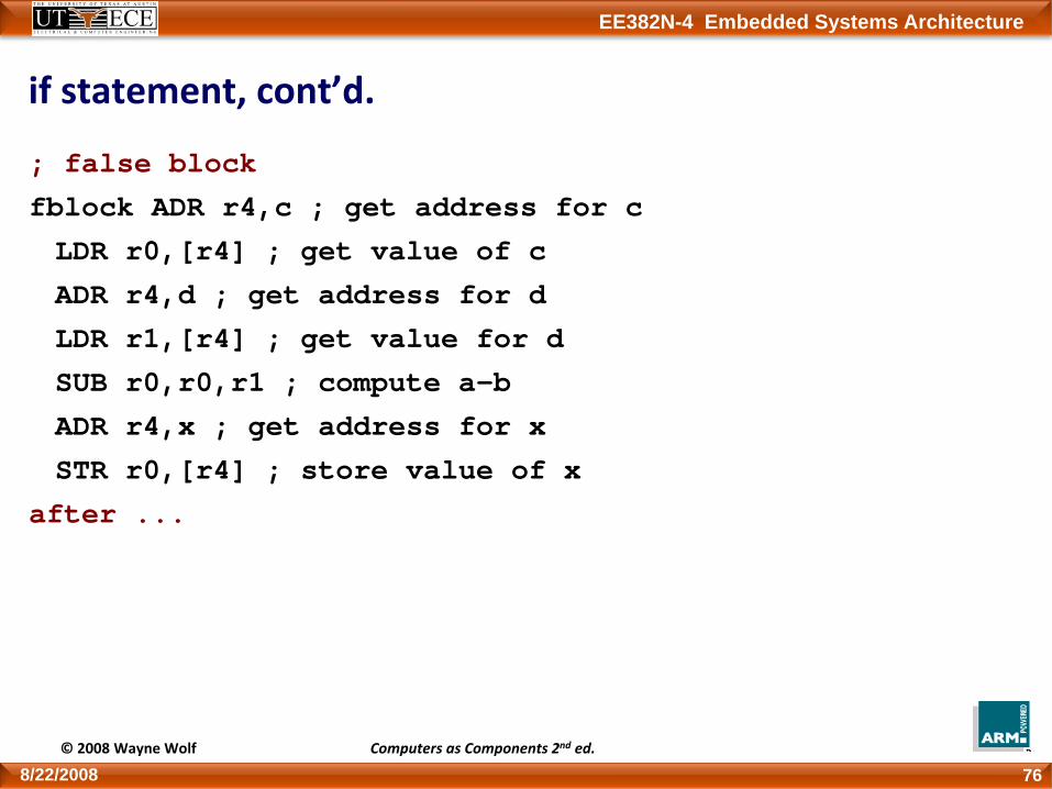
if statement, cont’d.
; false block
fblock ADR r4,c ; get address for c
LDR r0,[r4] ; get value of c
ADR r4,d ; get address for d
LDR r1,[r4] ; get value for d
SUB r0,r0,r1 ; compute a-b
ADR r4,x ; get address for x
STR r0,[r4] ; store value of x
after ...
768/22/2008© 2008 Wayne Wolf Computers as Components 2nd ed.
EE382N-4 Embedded Systems Architecture
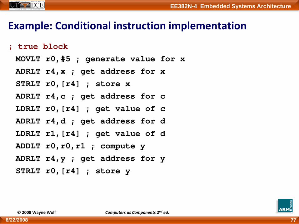
Example: Conditional instruction implementation
; true block
MOVLT r0,#5 ; generate value for x
ADRLT r4,x ; get address for x
STRLT r0,[r4] ; store x
ADRLT r4,c ; get address for c
LDRLT r0,[r4] ; get value of c
ADRLT r4,d ; get address for d
LDRLT r1,[r4] ; get value of d
ADDLT r0,r0,r1 ; compute y
ADRLT r4,y ; get address for y
STRLT r0,[r4] ; store y
778/22/2008© 2008 Wayne Wolf Computers as Components 2nd ed.

EE382N-4 Embedded Systems Architecture
Conditional instruction implementation, cont’d.
; false block
ADRGE r4,c ; get address for c
LDRGE r0,[r4] ; get value of c
ADRGE r4,d ; get address for d
LDRGE r1,[r4] ; get value for d
SUBGE r0,r0,r1 ; compute a-b
ADRGE r4,x ; get address for x
STRGE r0,[r4] ; store value of x
788/22/2008© 2008 Wayne Wolf Computers as Components 2nd ed.
EE382N-4 Embedded Systems Architecture
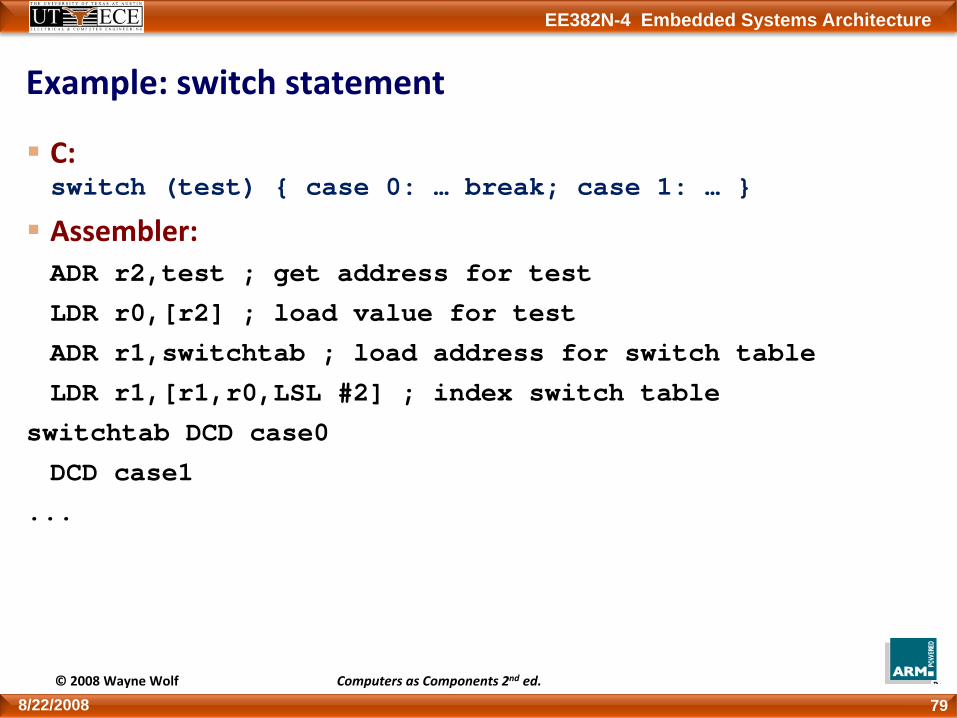
Example: switch statement
C: switch (test) { case 0: … break; case 1: … }
Assembler:ADR r2,test ; get address for test
LDR r0,[r2] ; load value for test
ADR r1,switchtab ; load address for switch table
LDR r1,[r1,r0,LSL #2] ; index switch table
switchtab DCD case0
DCD case1
...
798/22/2008© 2008 Wayne Wolf Computers as Components 2nd ed.

EE382N-4 Embedded Systems Architecture
Example: FIR filter
C:for (i=0, f=0; i<N; i++)f = f + c[i]*x[i];
Assembler; loop initiation code
MOV r0,#0 ; use r0 for I
MOV r8,#0 ; use separate index for arrays
ADR r2,N ; get address for N
LDR r1,[r2] ; get value of N
MOV r2,#0 ; use r2 for f
808/22/2008© 2008 Wayne Wolf Computers as Components 2nd ed.

EE382N-4 Embedded Systems Architecture
FIR filter, cont’.d
ADR r3,c ; load r3 with base of c
ADR r5,x ; load r5 with base of x
; loop body
loop LDR r4,[r3,r8] ; get c[i]
LDR r6,[r5,r8] ; get x[i]
MUL r4,r4,r6 ; compute c[i]*x[i]
ADD r2,r2,r4 ; add into running sum
ADD r8,r8,#4 ; add one word offset to array index
ADD r0,r0,#1 ; add 1 to i
CMP r0,r1 ; exit?
BLT loop ; if i < N, continue
818/22/2008© 2008 Wayne Wolf Computers as Components 2nd ed.
EE382N-4 Embedded Systems Architecture
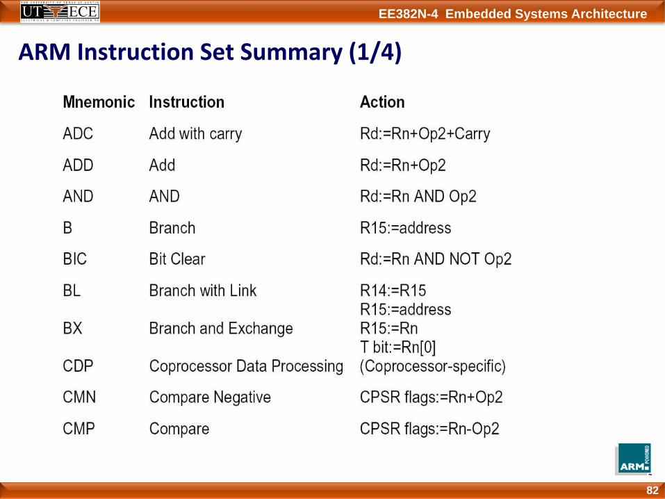
ARM Instruction Set Summary (1/4)
82

EE382N-4 Embedded Systems Architecture
83
ARM Instruction Set Summary (2/4)

EE382N-4 Embedded Systems Architecture
84
ARM Instruction Set Summary (3/4)

EE382N-4 Embedded Systems Architecture
85
ARM Instruction Set Summary (4/4)