the affects of high density plasma oxide deposition on
TRANSCRIPT
Lehigh UniversityLehigh Preserve
Theses and Dissertations
1999
The affects of high density plasma oxide depositionon CMOS transistor characteristicsMichael D. GrossLehigh University
Follow this and additional works at: http://preserve.lehigh.edu/etd
This Thesis is brought to you for free and open access by Lehigh Preserve. It has been accepted for inclusion in Theses and Dissertations by anauthorized administrator of Lehigh Preserve. For more information, please contact [email protected].
Recommended CitationGross, Michael D., "The affects of high density plasma oxide deposition on CMOS transistor characteristics" (1999). Theses andDissertations. Paper 582.
brought to you by COREView metadata, citation and similar papers at core.ac.uk
provided by Lehigh University: Lehigh Preserve

pross, Michael D. .,
.The affects of highdensity plasma ..oxide .deposition .on CMOS··transistor·
~eharacteristics ..
'. I, i
.Ma\/31· .1-999 .. .~~~\C;:~~~~!t'.;=~Fi'j::?;i··?t''''"F!:1?E£'.s;Jf2:;;:':~~';2~",,;~g~~Z~'5;1-7:":::;2··:·J:~:3)·:'.,~:.· ••.·;2~;;;.:CE:;:S~,;::":':;:'~"".22.;;j,~,;.:;'-';;;.~,!;;"";::~=-i§,0;;;;:£~:·,,,',':.Efjii;F::';',~,E;·',':5:'-&
. ,

- .
THE AFFECTS OFHIGH DENSITY PLASMA
OXIDE DEPOSITION ON CMOSTRANSlSTOR CHARACTERISTICS
by
Michael D. Gross
. A Thesis
I .Presented to the Graduate and Research Committee
of Lehigh University
in Candidacy for the Degree of
<. Master of Science
in
Electrical Engineering
Lehigh University
May 1999
..

Acknowledgments
I would like to thank Dr. Marvin White for his support in this endeavor. His expertise in
the solid state field, coupled with vast experience in industry has provided unique insight
to b~th this thesis and my personal career. I would also like to thank Dr. Charles Pearce .
for his help and patience in answering endless questions-during this project and
throughout my graduate studies. .
I would like to acknowledge Lucent Technologies for providing the necessary
funding to process many additional experimental lots, resulting in significant p~ocessing
costs.
Finally, I would like to thankmy wife Deborah, and son Stephen for their support,
sacrifices, and understanding during my graduate work.
iii ,
!J

iv

Contents
Acknowledgments ' 111
List of Tables V1I
List ofFigures Vll
Abstract 1
1 Introduction 3
1.1 Historical Review..~.
3
1.2 Motivation for parametric study 7---J
1.3 Scope ofthesis 8
2 Theory ofPlasma Damage 9
2.1 Damage History 9
2.2 Mechanisms for Damage 11
3 I-V tests 14
3.1 Transconductance 16
3.2 Threshold voltage 19
3.3 Saturation current - Ion 21
3.4 Leakage current - Ioff 22
v

4. r,·
Experiments .24
4.1
4.2
0.55 micron Technologies
0.35 micron Technologies
24
24
5 Conclusions 25
References
Appendices
A .' HDP deposition machine description!
Vitae
vi
26
28
28
3.1

List of Tables
3. 1 List of lots processed and individual cell experiments 15
List of Figures
1.1 "Breadloaf' coverage ofoxide 5
1.2 Gap fill progression with HOP 6
2.1 Fowler-Nordheim Tunneling 12
2.2 Direct Tunneling 13
\ 3.1 0.55 micron p-channel transconductance 16\
3.2 0.35 micron p-channel transconductance 17
3.3 I-V plot to determine threshold voltage and transconductance 18
-3.4 0.55 micron p-ch~el threshol? voltage 19
3.5 0.35 micron p-channel threshold voltage 20....
3.6 0.55 micron p-channel Ion 21
3.7 0.35 micron p-channel Ion 22
3.8 0.55 micron p-c~annelloff 23
3.9 0.35' micron p-channel loff 23
A.I Electrical Chamber Schematic 30
vii
. ~
\
Abstract
The affects ofHigh Density Plasma (HDP) oxide deposition on Complimentary
Metal Oxide Semiconductor (CMOS) devices during the manufacturing process is
ex8:ffiined. The device parameters of transconductance, saturation current, gate leakage
current, and the threshold voltages ofminimum channel length transistors are studied.
Both p-channel and n-channel device parameter variations are studied with respect to,
varying HDP deposition conditions and standard Plasma Enhanced
TetraEthylOrthoSilicate (PETEOS) oxide dielectri~ films.
High Density Plasma processing equipment has become an important part ofthe
Illanufacturing process for subrnicron CMOS devices. HDP processing is used for pattern
etching ofthin films and deposition of insulating oxides. The plasma gene~ated in this
equipment takes place at extremely low pressures and has a much higher ion density than .
processing equipment used for the last 20 years of integrated circuit manufacture. This
has led to concerns over device damage due to plasma charging, ion bombardment, and
UV radiation. Two groups ofdevice structures are analyzed for this investigation, a 0.55
and 0.35 micron CMOS Twin Tub process. Historically, these fi.nely balanced, and
relatively mature technologies have shown a 'sensitivity to process changes.
1
.'
/

The HDP deposited films studied here are used for the interlevel metal dielectric.
At this point in the manufacturing process, the transistors have been formed and are
susceptible to several types of damage. Plasma charging during deposit is ofparticular
concern. Uneven plasma fields and topography dependent charging have been identified
as sources ofuneven electrical potentials that cause c~rrents to circulate through the
device and damage the gate oxide during the manufacturing process.
The data presented shows small decreases in the P-channel threshbld voltages on, .
devices withthicker gate oxides. This is consistent with literature showing how thinner
gate oxides are subject to a higher degree ofless damaging Direct tunneling, rather than
the more destructive Fowler-Nordheim tunneling dominant above lOq angstroms ofgate
.thickness. The selective P-channel damage observed is explained by the posithre plasma,
which creates an accumulation of electrons under the gate'electrode with an increase in
electron flow across the gate and damaging Fowler-Nordheim tunneling current flow to
the N tub below. The electron accumulation causes a depletion region in the N-channel
device which protects the N-channel from damagi~g current flow.
2
...
Introduction
1.1 .Historical Review
Integrated circuits. are fabricated on thin disks of silicon four to twelve inches in
diameter, with eight inch currently the most popular size for high volume production.
These disks, or wafers as they are commonly called, are sequenced through a process
routing of several hundred stepsto produce a completed device wafer. Each wafer
contains up to several hundred individual devices which are subsequently cut apart arid
individually packaged. Each ofthese devices can contain millions oftransistors with the .-
smallest geometry approaching one tenth ofa micrometer. Wafers are typically processed
in batches of 25 wafers per standard cassette.
The entire circuit fabrication process takes place in a "clean room" environment
where air is filtered to remove particles an order ofmagnitude smaller than the smallest
device geometry. Within this manufacturing area, there are several specialized
processing areas each with its own unique capabilities. The early history ofintegrated .
circuit processing included many batch processing operations where up to 100 wafers at a,
time were loaded, many times by hand, into specialized fixturing for eacl:idifferent piece of
equipment. Today, the trend has been toward single wafer processing within each
processing tool, using automated handling fro~ the standard travel cassette to a central
robot feeding individual chambers for processing and then returning to the cassette to be
moved t.9 the next piece of equipment. The HOP process under study runs on this type of:....=-_---=-._- ~
3
equipment which provides extremely uniform within wafer processing variations, as well
as minimal wafer to wafer variations.
As wafer sizes have grown from one inch substrates in the early 1960's to the most
common eight inch substrates today, transistor minimum channel lengths have shrunk two
. .
orders ofmagnitude and now approach one tenth of a micrometer. When the minimum
dimension oftransistors dosed in on two micrometers, the packing density oftransistors
became so high that one level ofmetal tran~istor interconnects became insufficient. A
second level ofmetal was required to accommodate all the connections. The insulating
layer between the metal runners became a problem because this film was deposited on thin
aluminum runners. The most conformal insulating oxide films at the time were produced,
in low pressure chemical vapor deposition furnaces operating above 700C, while the0I •
aluminum covered wafers could no~ be subjected to temperatures above 450C. This led to
Plasma Enhanced Chemical Vapor Deposition (PECVD) being used for the intermetal
dielectric.
PECVD oxide films at ~400C served as a suitable alternative. Plasma enhanced
films are produced using a radio frequency power source to provide energy to the reaction
which allows a lower deposit temperature. The solution using straight PECVD films was
short lived because ofanother physical limitation. The deposited oxide films ''balloons
out" while covering the metal runners and causes a 'breadloaf' effect at the tops ofthe
metal (Figure 1.1). When the spacing between the metal runners became less than one
micrometer, the oxide coverage closed the gap at the top before the space was filled in
with oxide.' This resulted in a void in the oxide coverage. The answer to the void problem
4
)

was to used a sputter etch on the oxide in between deposits, etching the top. comers of the
oxide over the runners at a 45 degree angle and allowing the subsequent oxide deposition
to fill the gaps between runners. There was some process divergence in industry at this
point in time, with the mainstream using TEOS based PECVD films with an etchback,•
while others used spin on~ or TEOS/Ozone processes to fill gaps and planarize
topography.
HDP-CVDDEPOSITION' ANDGA'P-FILL MECH~AN·ISM
~pPsitiQn'Only .
(<:. 1.1 - 1.2 tldr)
Deposition+ln$ituSputtering.. ,' -: ':-',---,.-. '. ..- .. ' .-.-. '." .. -:'----.. ',' .. '.' ".--. ''-'',-,
Figur~}.1: ''Breadloaf' coverage of oxide and result of sputtering during deposit
ndr =net deposition rate
5
\.

The alternative gap fill processes were adequate down to 0.5 micron technologies,~ .
but below that, they have reached their gap fill limitations. High Density Plasma
deposition has come on as a promising new technology. HDP films are capable offilling
gaps down to the limits of current technology. Argon gas is used during the deposition
process to sputter etch concurrently with the deposit (Figure 1.2). The resulfis a high
quality film that meets the physical requirements for the device, but has questions
pertaining to process induced transistor damage........
Gap-FHlEvolution
Figure 1.2:.Gap fill progression with'HDP
6

Many new technologies are being developed with HDP technology. HDP
deposition has opportunities for future production processes with the addition of fluorine.
The dielectric constant of the deposited oxide is reduced with flourine as a dopant, and. .
device speed can be improved on those advanced devices that have interconnect delays as
a limiting factor.
1.2 Motivation for parametric study
The fabrication process for a sub-micron CMOS integrated circuit is a delicate
balance ofthermal budgets and process interactions. An established production line has
many checks and balances to prod1;lce a high performance device. New technologies are
using HDP throughout their development and evaluate overall damage to the device. This
study concentrates on the interactions ofHDP deposits with established production
technologies. The 0.55 and '0-35 micron technologies under study have been running in
volume production for a significant period oftime and have established I-V parametric
ranges and behaviors which can be ea.sily upsetby a ne'Wpr~cess technology replacing a
. process under which the device was characterized. For this reason, many older
technologies do not take advantage ofnew processing developments.
7

By combining the deposit-etch-deposit sequence into one process step, HDP
deposition has the potential to improve fabrication cycle time, reduce defects and improve
. .yields. Intel has recently ~ounced a ne"Y high performance 0.18 mi~ technology that
used fluorine doped HOP oxide to provide a lower dielectric constant and has shown
speed improvements of 14% over standard oxide films [1]. These advantages make HDP
attractive' to both oM and new technologies. Applied Materials, one ofthe industry
rers in this type ofequipment; has recently announced the shipment of its 100ili system
(most still in development), compared to thousands of systems shipped using the older
PETEOS tethnology, demon,strates the immaturity of the process and the need for more
detailed study.
1.3 Scope of Thesis
The purpose ofthis thesis is to determine the way HDP deposition affects the I-V'-
characteristics of CMOS devices and how it impacts the implementation ofthis
manufacturing process on established technologies in high volume production.
Specifically, explaining why only p-channel devices are affected only on technologies with
thicker gate oxides.
8
2 Theory of Plasma Damage
2.1 Damage History
Device damage was first identified in the 1970's as "radiation damage" and neither
the mechanisms nor the level of damage were completely understood. As the gate oxides
thinned through the 1980's; "charging damage" was the topic of interest. The general
prevailing theory ofthe time was that positive charging on the wafer surface led to
Fowler-Nordheim tunneling in the gate oxide[2]. Damage Models became more complex
and research began to explain charging patterns across the wafer[3]. Plasma chemistries
were initially used for etching circuits, thus earlier studies focused on etch processes. The
etch studies showed damage occurred at endpoint and during over etch [4], and was
insignificant during initial etching, plasma ignition and extinction[5].
More recent studies consider both etch and deposition plasmas as well as multiple
frequency radio frequency sources [14]. The trend in process chemistries has been toward
extremely low pressures and high ion densities which have increased the damage potential.
Specific charge test wafers are used at present with antenna structures characterized by
area ratios of 100,000: 1. Other specialized test structures include large aspect ratio,
densely packed metal runners that promote topography induced charging.
Damage that scales ~th increased area indicates charging affe.cts. Another
relatively new charge analysis tool is the Contact Potential Difference or the Surface
Potential Measurement, where the voltage potential of the surface of a thick oxide is"'." . .
. mapped across a wafer [6]. This technique hasbeeri used to solve one ofthe classic atld
"9
most far reaching cases ofplasma damage that has been documented in processing history..,
[7]. One ofthe major manufacturers ofPECVD oxide 'used a low power inert plasma at
the ,end ofthe deposit to remove a static charge on the wafer that caused the wafer to
stick to the deposit fixturing that held the wafers. This "power lift" step solved the
sticking problem, but left a severe charge in the oxide. Since this charge was incorporated
into a process that was used for devices on the order of one micron, no significant
difference was observed until transistors shrank below a half micron. Then, as new
te~logies were phased in, problems with device yield started to become apparent with
gate oxide failures. Caution must be exercised in evaluating charge distributions with
, SPM because it only gives a snapshot of the very last operation in the plasma chamber.
These measurements were originally interpreted as representing the charge in th~ entire
film.. Modern PECVD deposition processes may layer multiple d~position conditions
within one thick oxide, and proper analysis requires stopping the process throughout the
. \ .deposit to take measurements.
It may appear that as gate oxides thin down and plasma densities increase, plasma
. damag~ may become a limiting factor in ULSI production, but tills is not the case.
Processing equipment manufacturers have improved both wafer coupling during deposit
and plasma uniformity such that damage resulting from charging currents are minimized.
Also researchers have demonstrated that gate oxide damage peaks as oxide thickness
decreases to roughly 100 angstroms, but begins to improve as the oxide thickness thins
below 100 angstroms [2]. This can be explained by a theory that attributes damage in
oxides above 100 angstroms to'Fowler-Nordheim tunneling and to oxides below 100
10

angstroms to direct tunneling, which causes less damage to the gate oxide [2]. These
factors should allow the continued scaling down ofdevices to at least the 0.1 micron
(lOOrim) feature size..
2.2 Mechanisms for .Damage
The primary concerns for damage with plasma processing are charging, UV
radiation, and ion bombardment. Ion bombardment is part of charging but can cause
problems with physically sputtering trenches at the base of tall features and increasing
overall surface roughness. UV radiation is' under investigation for causing direct line of
sight damage rather than typical surface charging and th.reshold voltage shifts have been
associated with this phenomena in HDP gate etches [8].
Surface charging in its most extreme form is the result ofuneven electric plasma
fields in the processing equipment anq poor wafer coupling to the plasma. Texas
Instruments reports on early HDP deposition tools showed 300 mV threshold voltage
shifts in P-channel devices [9]. The latest generation ofHDP equipment has minimized.
these extreme affects and the general mechanism for damage is topography dependent
charging [10]. HDP deposition charging occurs with high aspect ratio metal runners being
bombarded by positively charged ions from the plasma. The electrons are shielded by the
positively charged runners and a net positive charge is presented to the surface. A current
can circulate through the gate. oxide. while the deposition process is taking place. At high
electric field strengths (>5MV/cm) on oxides greater than 60 angstroms, Fowler- ,
11

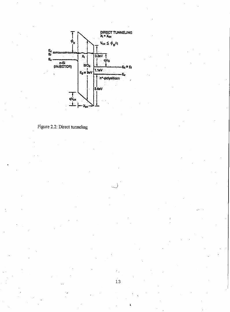
Nordheim tunneling, (Figure 2.1), takes place which causes damage to the oxide by the
energy released from electrons which break bonds or can fill traps. Below gate oxide
. .thicknesses of40 angstroms is where Direct tunneling, (Figure 2.2), dominates and
electrons pass through the oxide with a minimum of reaction[11]. Trap assisted
tunneling can also be a factor in this range of oxide thicknesses.
n-Sl.(INJEeTOR)
IqVqS
F-N TUNNELING:
Xt·~SXox·
Vox '2=. epslq
,
~""";,.;&,.---Ec. Ef
~~Iz:r- ..........................-e.,""'~)'$!llcon.
Fi~re 2.1: Fowler-Nordheim tunneling
12
S102 Ec"Et
F.ga~vt.1eV .....•.. •. Ewn+...potyallicon
~Et =-=.==._=.~Ie--""(-..I.
Ert----..."I'-$i
(INJIWTOR)
3.8eV
T 1··qVox ....-L."" .'"~~"
Figure 2.2: Direct tunneling
13

3 I-V tests
The I-V measurements were taken on 5 sites per wafer (top~ bottom, left, right,
and center) and ten to fifteen wafers per group. Therefore each bar within each cluster
represents the average of 50 to 75 transistor measurements. Each bar cluster represents aseparate group (lot) ofwafers processed under conditions listed in Table 1. Refer to the
experiments section for a description of individual group conditions. There were no
significant differences in the n-channel devices measured for any of the parameters under
study, thus only the p-channel data is presented.
The charging taking place during deposit is a positive charge. This positive charge
attracts electrons under the gate oxide to essentially make a depletion area in the p-tub and
a restriction to the plasma charging circuit that circulates through the gate, oxide, tub, and
substrate. Tunneling currents are thus prevented from damaging the oxide in n-channel
devices. P-channel devices are susceptible to these currents because the accumulated
electrons under the gate electrode .increase the electric field across the oxide, thereby,
enhancing the flow oftunneling current. The result is observed a's an increase of damage
inp-channel devices as compared with n-channel devices.
·fJ
14
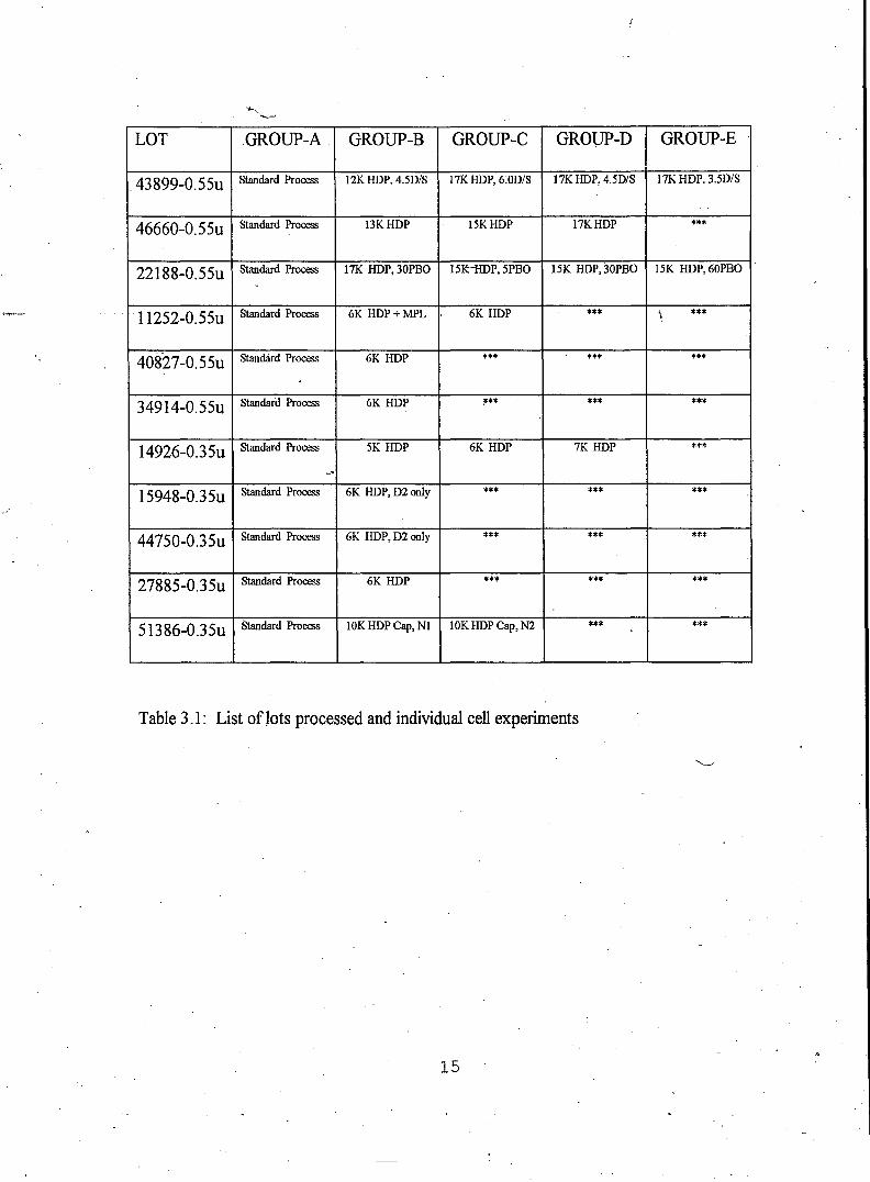
LOT GROUP-A GROUP-B GROUP-C GROuP-D GROUP-E
43899-0.55u Standard Process 12K HDP, 4.5D/S 17K HDP, 6:0D/S 17K HDP, 4.5D/S 17K HDP, 3.5D/S
46660-0.55u &'tandard Process 13KHDP 15KHDP 17KHDP ***
22188-0.55u Standard Process 17K HDP,30PBO 15K:-HDP,5PBO 15K HDP,30PBO 15K HDP,60PBO,
11252-0.55u Standard Process 6K HDP+MPL 6K HDP *** '\ ***
40827-0.55u Standard Process 6K HDP *** *** ***
34914-0.55u Standard Process 6K HDP ~** *** ***
14926-0.35u Standard Process 5K HDP 6K HDP 7K HDP ***
~
15948-0.35u Standard Process 6K HDP, D2 only *** *** ***
44750-0.35u Standard Process 6K HDP, D2 only *** *** ***
27885-0.35u Standard Process 6K HDP *** *** ***
51386-0.35u Standard Process 10K HDP Cap, Nl 10KHDP Cap, N2 *** ***
Table 3.1: List oflots processed and individual cell experiments
15

• gm - Standard
Il:lgm -8
lllIgm-C
lilgm -0
mgm-E
3.1 TranscQnductance (gm)
Transconductance measurements were made on the devices by placing -5V on the
"drain, ground to the source and tub, and varying the gate voltage from 0.5 to -4.0 volts in
-0.1 volt increments. The transconductance is calculated as the change in drain current
divided by the. change in gate voltage in the linear region ofthe curve. The gate voltage
was increased until the slope ofthe Id vs Vg curve begins to decrease, indicating a end to
the linear region ofthe curve. The linear portion ofthe curve is extrapolated back to
where it crosses the Vg axis and this is the value used for threshold voltage.
P-channel (small) gm (O.55u)
1180.---------------~'----__,1160 .j-----m~ira-----------------l,- ----,
~~~ +-.m,,,~--.~l-. ---. --
1100 11---.i~1l-:il-_-_-_-liffii!f--......-
~1~0:40 ~1---.lt11l--~--~~l\1-- __1;,,'.1l---
1020 ~'jl--__lr:,:;,L,..,~,:..,.!''---·,:--l~il ::lr-1000 t--""'--+-""'----+
40827 34914 43899 46660 22188 11252
Figure 3.1: 0.55 micron p-channel transconductance
-,1
16

P-channel (small) - gm (O.35u)
• gm - Standard
IlIgm - B
IIIIgm-C
IIgm - D
Bgm -E
1000
1200-1----
1600 -j-------------
1400-j-------------
20001800 ------------------------------------------------ -----------------------------------,--------.---------------------------------------------]
f~i~I--------;
11----~J~!~;I----
m~ll
27885 14926 15948 44750 51386
Figure 3.2: 0.35 micron p-channel transconductance
There were no significant observable changes in the maximum ofthe
transconductance with ~ither the 0.35 or the 0.55um technology.
Ifthe maximum gm changes, then this indicates a build-up in interface traps due to
the d~mage~However, if the curve shifts to the right or left, then there is a build-up of
tied charge. Sometimes both are observed.
17

-II)
/
/.:/. ,
~,
,I
-v5
\'
7
Figure 3.3: I-V plot to detennine threshold voltage and transconductance
18~ .

·3.2 Threshold voltage
The threshold voltages were extrapolated from the Id vs Vg curve as covered in
the transconductance section.
P-channel(small) - Vt (O.55u)
1.1 ..-------------------,---------,1.00+-r--------------------l1.08 ,-------,
irJ.':iI-! --,--- --j .vt - Standard
~:~ ~I~~~!~l-----------------__i [lvt - B
~:~ (:il-i-----.-------------------j :~~~
~.~ ~:,..,..i".:f:".l.!",..:'-. ~..,',:.:,i;,.!"[.,.,,i·l-.- __!~~~t---.=- mVl - E1.01 ~~.- ~;!}---'--.If--l?&t-1
4:Rt2.7 34914 43899 22188 11252
Figure 3.4: 0.55 micron p-channel threshold voltage
19

P-channel (small) - Vt (0.35)
• Vt - Standard
IlIVt - B
mVt -c .IBVt - 0
EI Vt - E11----if!~I----
0.92 ,---------------------,
0.9+------.,.--
0.88 -t----
0.86
0.84
0.82
0.8
27885 14926 15948 44750 51386
Figure 3.5: 0.35 micron p-channel threshold voltage
The threshold voltage was the only parameter that had any significant variance
with HDP processing. Figure 3.4 shows a lower threshold voltage for every cell ofHDP
processing compared to the standard deposit/etch!deposit process, although this is not the
case for the product with thinner gate oxides in figure 3.5. The one exception (11252B) is
one HDP cell with a higher Vt that used a Metal Protection Layer (MPL) before the HDP ,
deposit. This was a 1000 angstroms ofless damaging standard plasma film deposited on
top ofthe metal runners. The MPL layer has been documented to show improvements in
damage for both Etch [12] and deposit [13]. These results are inagreement with
previously stated plasma damage theories that support only damage to the P-channel
devices and the direct tunneling causes less damage to the thinner gate oxide device
[12,13]. These small changes in threshold voltage are significant because each and every
lot showed a 10 to 20 mV change.
20
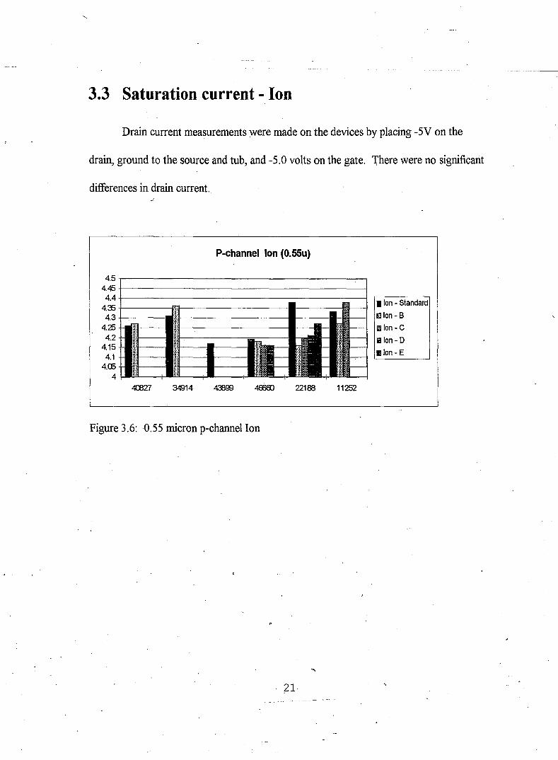
3.3 Saturation current - Ion
Drain current measurements were made on the devices by placing -5V on the
drain, ground to the source and tub, and -5.0 volts on the gate. 'rhere were no significant
differences in drain current.
P-channel Ion (O.55u)
4.5,---------------------,4.45 +---------------------1
4.4 r-.-1o-n --S-ta-nd-ar--'d
444.3525.3 :====-=-=-~fm:.r.~,..,·~.,r"~.,:.,.,~,~".,i;r-,i,,.--------._----l!JII---1 1311II" I,oonn ~ Be
~~it------1·>"I----------------'~~j4.2 ~~ ,,' I~ lilian - D4.15~] ~l----__-- ~ lilian _E
4~ ~ml-----1·:.~.;[i,.l---111---- i~4 ~ !t.i +-Wl~l""""---1
40027 34914 22188 11252
Figure 3.6:0.55 micron p-channel Ion

• Ion - Standard
Ii!! Ion - B
III Ion - C
Blion - D
!3lon - E
um 1 _
I
11!l-:--
i!)~f----
!J, _
1""-----
54.8+----4.6+---4.44.2
43.83.63.43.2
3
27885 14926 15948 44750 51386
Figure 3.7: 0.35 micron p-channel Ion
3.4 Leakage current - loff
Leakage current measurements were made on the devices by placing -5V on the
. drain, ground to the source and tub, and vary the gate voltage from 0.5 to -4.0 volts in
-0.1 volt increments. ThVe were no significant differences in leakage current.
22-\

I
---P-ehannel-to1t(O;55u)
---------------------------------_._-------_..~-- ..-------~-_._---.------------_. __ ._-
""'• Joff - Standard
[Jloff- B
B1loff - C
Bloff- 0
.Ioff - E
11252221883491440027
------1--- ---11.911.8 -1--------------11.7 -I-==------------I._-IE11.6 ~iil--;---I.if.ill-----t,11.5 ii:t------.,f.jif,'.i.:.,I-----
~~11.4 ~r------'~t'iI--; --.'!!It
~ ~:~ +-.p~r---- t,r~'.,l.t.:;t--".;1---_-_-_--I__E~ ,
11.1 'i'ir-------t.;~.:11 +--"",j~'-----Ic--=- ---\--
Figure 3.8: 0.55 micron p-channel Ioff
P-channel loff (O.35u)
iii-:--
11----I
• loff - Standard
!llIloff - B
IS Ioff - C
IlIloff - 0
mloff - EIii-'------."
}i
!~H;j-:----------'
11-----
11.6
11.4-+------------11.2 -+--=,.-----
,;~ Il--'---10.6 '-*,1-----~~.~ 1+1----
1027885 14926 15948 51386
Figure 3.9: 0.35 micronp-channel Ioff
23

-4----E-~periments---- --.- . -.-.-
4.1 0.55 micron Technologies
....~._-~....._.._-_.-._-~--,--~-_._~
The 0.55 micron technologies used for this project are double level metal twin tub
CMOS logic testers. They have 125 angstrom gates and use aluminum interconnects.
The standard processing to fill the inter metal dielectric uses two plasma enhanced TEOS
deposits with al). Argon sputter etch between the two deposits. The standard HDP
... conditions are a 6000 angstrom (6K) film comprising of2K ofa 4.5 Deposit to Sputter
(DIS) ratio, and 4K of6.0 DIS. The lower the DIS, the higher the sputtering component,
which provides a better gap fill with a higher damage potential. The Pre Bias Off(PBO)
step is used at the end of deposit to tum off the deposit gases while continuing to sputter.
Longer PBO times can help planarize topography.
4.2 0.35 micron Technologies
The 0.35 micron technologies used for this project are three level metal twin tub
CMOS logic testers. They have 90 angstrom gates and are essentially a shrink ofthe 0.55
micron process. All lots in this thesis except 51386 are used to evaluate HDP as the inter
level dielectric. Lot 51386 uses a 10K HDP oxide as part of the final encapsulation ofthe
device on top ofthe third level ofmetal, with standard processlng being a thinner 3K of
plasma enhanced TEOS.
------.IilIo5.------IIeonclus-iuns-- ~~~~~----
The data presented shows small decreases in the P-channel threshold voltages on
devices with thicker gate oxides. This is consistent with literature showing how thinner
gate oxides are subject to a higher degree of less damaging Direct tunneling, rather than
the more destructive Fowler-Nordheim tunneling dominant above 100 angstroms ofgate
thickness. The positive plasma charging causing a depletion region in the N-channel device
which protects the N-channel device. However, the same positive plasma creates an
accumulation regime for the P-channel device, which results in an increased field across
the oxide and the flow of significant Fowler-Nordheim tunneling currents. A l}oteworthy
observation was the apparent reduction in damage using the Metal Protection Layer. This...
thin, non-damaging oxide layer, deposited between the metal and the High Density Plasma
oxide layer, has promise for minimizing process damage and will be considered in future
experiments.
Equipment manufacturers ofHigh Density Plasma systems have tuned out plasma
field uniformity problems to a degree which provides a process damage level nearly _
-equivalent to standard plasma oxide processing. Process deposition specifics, partic&f.irly
the Metal Protection Layer, can be useful in optimizing particularly sensitive devices.
25-

References
1 S. Yang et aI., "A High Performance 18.onm Generation Logic Technology, IEDM
Technical Digest, 1998, p.l97-200
2 C. Hu, IEDM Technical Digest, 1996, p.319
3 Namura et aI., "Charge buid up in magnatized plasma process", Dry Process
Symposium 1990, p. 135
4 S. Ma and 1. P. McVittie, Symposium on Plasma Process Induced Damage, May
1996 American Vacuum Society
5 Shin, Noguchi and Hu, "Thickness and other effects on oxide and interface damage
by plasma processing", Proceedings ofIRPS 1993, p. 272 ..
6 K. Nauka et aI., ''Monitoring ofDielectric charges introduced by plasma
processing with contact potential difference and surface photovoltage
measurements", Plasma Etch Users Group May 1995
7 K. Cheung, "Is Surface Potential Measurement a useful charge damage
measurement method?" Sym,posium on Plasma Process Induced Damage, 1998
American Vacuum Society, p 18
8 G. Bersuker et aI., "Transistor degredation due to radiation in a high density
plasma", Symposium on Plasma Process Induced Damage, 1998 American
Vacuum Society
26

11 C. Gabriel, CEE, DC, Berkeley, Oct. 1998, chap.2
14 Pearce, Fetcho, Gross, Koefer, Pudliner. "Characteristics of silicon nitride
Rockwell Proc. SPIE, Volume 3212
IEEE Ele. Dev. Letters, vol. 15, no. 8, August 1994
radio frequency source" Journal ofAppliedPhysics 71(4), 1838-41, Feb. 1992
deposited by plasma enhanced chemical vapor deposition using a dual frequency
Phys., 33,1994, p. 6013
S. Krishnan and S. Nag~Y1TIROsium onPlasma process Induced Damag~, 1996~
American Vacuum Society\.J
13 D. y.: C. Lie, "Hot...;Carrier Degridation Introduced by Backend Processing", -
12 C. Gabriel, "Gate Oxide damage reduction using a protective dielectric layer",
10K. Hashimoto, "Charge damage caused by electron shading effect", .Jpn..J. Appl.
9
27
Appendices
A HDP deposition machine description
The equipment used is a standard system available from Applied Materials, Inc.,
model 5200 Centura. The machine handles up to four single wafer process chambers,
connec~ by a central robot. The single wafer process chamber is completely ceramic
inside and virtually maintenance free. After each wafer is deposited, the wafer is removed
and a microwave activated flourine gas is used to clean the residual oxide in the chamber.
This is followed by a short deposit to condition the chamber and seal any flourine residue
from the clean.
...
/
28

----:---~--"--~---_._-
The top ofthe chamber is a dome with radio frequency energy being supplied by
coils on the outside driven by 1.8 and 1.4 MHz generators that provide an inductively
coupled plasma inside the chamber when the process gasses are added. The wafer sits on
an electrostatic chuck which is powered by a DC bias for holding force, and a 13.56:MHz
generator to direct the ion flux from the plasma to the wafer (Figure A.l). This
electrostatic chuck pulls the wafer flat on the chuck"and holds it down with enough force
so that helium can be pressurized on the wafer backside to cool the wafer, as well as
helping to develop the necessary bias to accelerate the Argon sputtering. Typically
deposited wafers are heated by either quartz lamps or resistance heaters, but this process
generates enough heat from the Argon sputtering component to elevate the wafer
temperature to above 600C and helium backside cooling is used to cool the wafer down to
approximately 400C. The oxide deposition is achieved using SiH4 and oxygen along with
the Argon sputtering component.
29

, ,
OOOOO~--l
SOURCE RFLOCAL MATCH
(TOP COIL) .
SOURCE RFLOCAL MATCH(SIDE COIL)
o
o HOP OXIDECHAMBER
oo
ELECTROSTATICCHUCK
RF SWITCH
RF FILTER
BIAS RFCABLE
DC/DCCONVERTER
E-CHUCK POWERSUPPLY BOARD ~--~
r------------III _I
IIII ELECTROSTATIC CHUCK POWER SUPPLY ASSEMBLY
------------~-----~
SYSTEMCHAMBER
CONTROLLER
BIAS RF MATCH& DC BLOCKING
CAPACITOR
r-CHUCK
.''h..
Figure A.I: Electrical Chamber schematic
30

Vitae
Michael D. Gross was born June 29, 1959 in Allentown, Pa. to Peter and Fay Gross. In
1979 he graduated from Lincoln Technical Institute with an Associate degree in
Electronics, and stared his 20 year career with Western Electric (Subsequently renamed
AT&T Microelectronics in 1984, and Lucent Technologies in 1996). Mr. Gross started
attending part time engineering classes at Lafayette College in 1981, and graduated in
1994 with a B. S. degree in Electrical Engineering. Part time graduate work at Lehigh
University began in 1995.
Mr. Gross has spent his entire career working with integrated circuit wafer
fabrication, and is currently a Member of the Technical Staff at Lucent Technologies. The
last ten years have been spent as a Senior Process Engineer in Plasma Enhanced Chemical
Vapor Deposition, with previous years spent in Plasma Etching. He possesses a patent for
machine fixturing that improves the uniformity of deposit in thin PECVD films and has co
authored a paper on dual frequency deposited films published in the Journal of Applied
Physics.
31

END
OF
TITLE""