texturing industrial multicrystalline silicon solar cells · texturing industrial multicrystalline...
TRANSCRIPT
Texturing Industrial Multicrystalline Silicon Solar Cells
D. Macdonald, A. Cuevas, M. Kerr, C. Samundsett, D. Ruby1, S. Winderbaum2 and A. Leo2
Centre for Sustainable Energy Systems, Dept. of Engineering, FEIT,Australian National University, Acton, ACT 0200, AUSTRALIA
1Sandia National Laboratories, Albuquerque, NM, USA2BPSolar, Homebush Bay, AUSTRALIA
E-mail: [email protected]
Three potential techniques for texturing commercial multicrystalline silicon solar cells are compared on thebasis of reflectance measurements. Wet acidic texturing, which would be the least costly to implement, producesa modest improvement in reflection before antirflection coating and encapsulation, whereas maskless reactive-ion etching texturing, and especially masked reactive-ion etched ‘pyramids’, generate a larger gain inabsorption. After antireflection coating and encapsulation however, the differences between the methods arereduced. Short-circuit current measurements on wet acidic textured cells reveal that there is a significantadditional current gain above that expected from the reduced reflection. This is attributed to both light-trappingand oblique coupling of incident light into the cell, resulting in generation closer to the junction.
1. INTRODUCTION
Multicrystalline silicon (mc-Si) solar cells currently account for around 50% of worldwide PV production, andtheir share of the market is steadily increasing. In general however, commercial mc-Si cells have lowerefficiencies than their single-crystal counterparts. One of the main reasons for this difference is the lack of a cost-effective method of texturing mc-Si, a process that is straightforward in single-crystal cells.
Texturing the front surface of a solar cell generally results in improved performance, mostly due to an increase inthe short-circuit current. This increase arises from three distinct mechanisms, all of which are related to the factthat the incident photons strike the cell surface at an angle.
Firstly, some light rays will be reflected from one angled surface merely to strike another, resulting in animproved probability of absorption, and therefore reduced reflection. Secondly, photons refracted into the siliconwill propagate at an angle, causing them to be absorbed closer to the junction than would occur with a planarsurface. This is especially relevant in material with diffusion lengths comparable to or less than the cell thickness,such as many multicrystalline silicon wafers. Thirdly, long-wavelength photons which are reflected from the rearsurface back to the front will encounter an angled silicon surface, improving the chance of being internallyreflected, either at the silicon interface or at the glass surface, and providing another chance for absorption. Thisfinal process is referred to as light-trapping, and gives an improved response to infra-red light.
Single-crystal silicon solar cells are generally textured with random pyramids, which are produced by etching inan alkaline solution such as KOH or NaOH. This is made possible by the anisotropic (i.e. orientation dependent)nature of these etching solutions, in conjunction with an appropriate choice of the crystal plane orientation at thewafer surface. The random nature of the crystal orientation of multicrystalline silicon wafers makes suchtechniques much less effective for this material because only a handful of grains are properly orientated. Inaddition, alkaline solutions can cause unwanted steps and crevasses between the grains. In this work, we examineand compare some of the texturing methods that appear to have potential as cost-effective processes. Specifically,wet acidic texturing and masked and maskless Reactive Ion Etching (RIE) processes are studied.
2. TEXTURING TECHNIQUES FOR MULTICRYSTALLINE SILICON
Numerous techniques for texturing mc-Si silicon have been examined in the past. Some have focussed on the useof RIE, either in conjunction with a mask to achieve large, regular features (Winderbaum et al, 1997), or withouta mask to produce much smaller and more random texture (Ruby et al, 1999). Other approaches have been basedon isotropic wet acidic etching (De Wolf et al, 2000). All of these methods produce lower reflection than can be
Texturing Industrial Multicrystalline Silicon Solar Cells Macdonald
ISES 2001 Solar World Congress 2
achieved with the standard alkaline damage-removal etch used today in industry.
Wet acidic texturing, performed with solutions containing HF/HNO3 which tend to etch isotropically, can resultin features with rounded surfaces, as opposed to flat-sided features which arise from anisotropic etches (de Wolfet al, 2000). These rounded features produce a scalloped surface that can have good reflection properties. Animportant issue with this technique is that the feature growth need to be ‘seeded’ in some way, otherwise a planarsurface will result. This seeding can be provided by surface damage caused during wafer sawing (maskless acidicetching), or, in more complex methods, by defined holes through protective layers such as oxides, nitrides orpolymers (masked acidic etching). In this paper we examine and evaluate a maskless acidic etching technique.Such a technique does not provide the extremely low reflection of some other methods, but does have theadvantages of being relatively easy to implement and low-cost.
Reactive Ion Etching (RIE) is a method for ‘dry’ etching silicon without the use of large quantities of liquidsolutions. It is based on placing wafers in a plasma of highly reactive ions. Under certain conditions, the etchingdynamics produce deep surface features that have excellent reflection properties. Like wet acidic etching, RIEcan be performed in a maskless fashion that produces somewhat randomly placed features, or in conjunction witha masking layer to produce more even features. In this paper, we compare the wet acidic texturing with both amasked and a maskless RIE texturing method. The maskless RIE texturing was performed at Sandia laboratoriesin the USA using a proprietary ‘metal-assisted’ process (Ruby et al, 1999). Masked RIE texturing was created byetching through phtolithographically-defined holes in a metal layer which is subsequently removed (Winderbaumet al, 1997). Both of these techniques offer promise for very low reflectance surfaces with minimal chemicalwaste, an issue that will become increasingly important in the photovoltaic industry. However, they are likely tobe more costly to implement than wet chemical methods.
3. RESULTS AND DISCUSSION
To provide a baseline with which to compare the three types of texture studied in this paper, we havecharacterised wafers from BPSolar’s current industrial alkaline-etching method for producing a damage-free, butoptically flat, surface. We have also studied as-cut wafers, which remain in the damaged state after wafer sawing.Because of the surface damage, they have relatively low reflection. However, the damage also produces manyregions of high recombination, which severely degrade cell performance. This highlights the important point thatgenerating good texture has to be coupled with a relatively damage-free surface.
3.1. Electron Micrographs of As-Cut, Etched and Textured Wafers
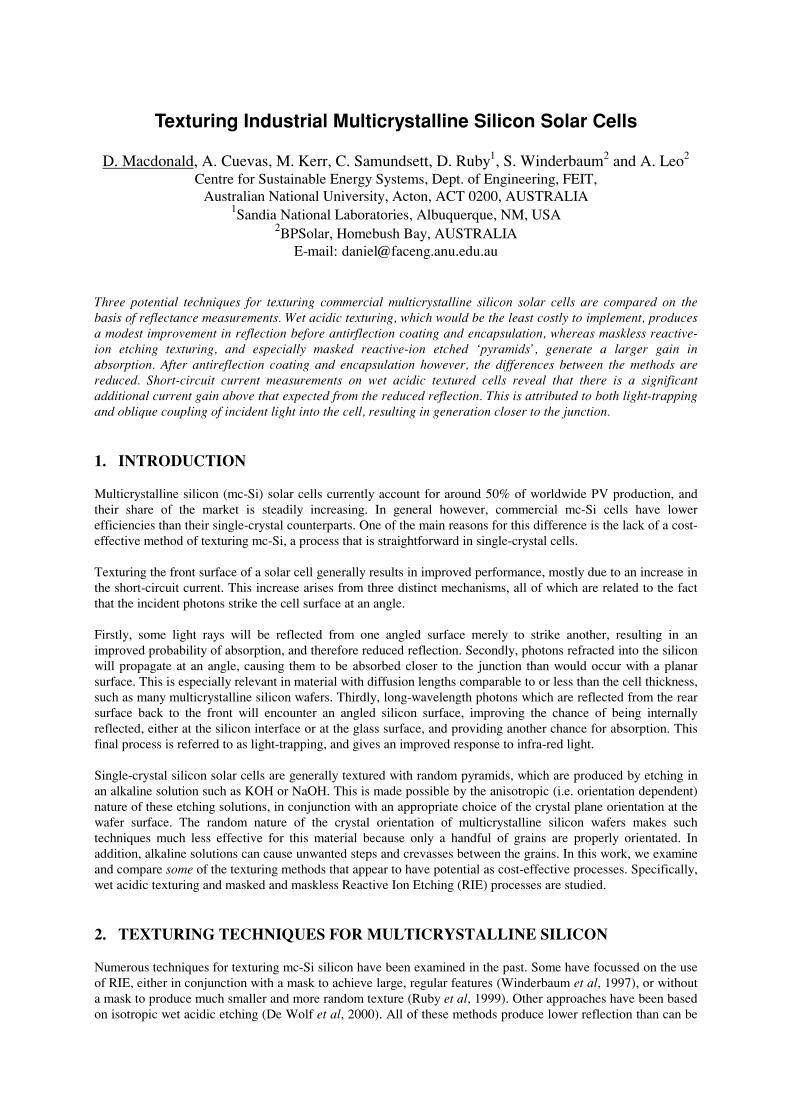
Figure 1 shows Scanning Electron Micrographs (SEMs) of multicrystalline silicon wafers with various surfaces.In the as-cut wafer (top two images), the heavy surface damage is evident as deep fissures and cracks, resulting inreasonable reflection control but high recombination. The next two images are of a standard industrial alkaline-etched wafer. It appears to have some texturing, but this is both shallow and highly grain-dependent, and whenaveraged over many grains is almost as reflective as a perfectly flat wafer. This reflects the fact that the alkalineetching solution used by BPSolar is relatively isotropic in comparison to solutions sometimes used for texturingsingle-crystal wafers.
The following two images are of an acidic textured wafer, which was performed with a HF/HNO3 solution. Awetting agent was added to produce more uniform texturing. Approximately 5-10µm of silicon was removedfrom each surface. Although the surface damage is removed, its original presence is nevertheless critical, since itacts as a seeding layer for the texturing. The resulting surface contains smooth sided, bowl-like features.
Figure 1 also shows images of the maskless RIE texturing performed at Sandia. These wafers have somewhatrandomly-placed but nevertheless deep features with steep sides, which provide very low reflection. Note that thefeatures of these RIE textured wafers are much smaller than those of the acidic textured sample (the two imageson the right have the same magnification, 5000×). Finally, a masked RIE textured wafer is also shown at thebottom of Figure 1. These features are very regular and steep-sided, with a distance of 7µm between pyramidpeaks. The pyramids are approximately the same size as the features on the wet acidic textured wafer.
Texturing Industrial Multicrystalline Silicon Solar Cells Macdonald
ISES 2001 Solar World Congress 3
Figure 1. SEM images of various mc-Sisurfaces. From top to bottom: as-cut (left1000×, right 5000×), alkaline-etched(both 500×, different grains), acidictextured (left 500×, right 5000×),maskless RIE textured (left 1000×, right5000×) and masked RIE pyramids(2000×, from Winderbaum et al (1997)).
Texturing Industrial Multicrystalline Silicon Solar Cells Macdonald
ISES 2001 Solar World Congress 4
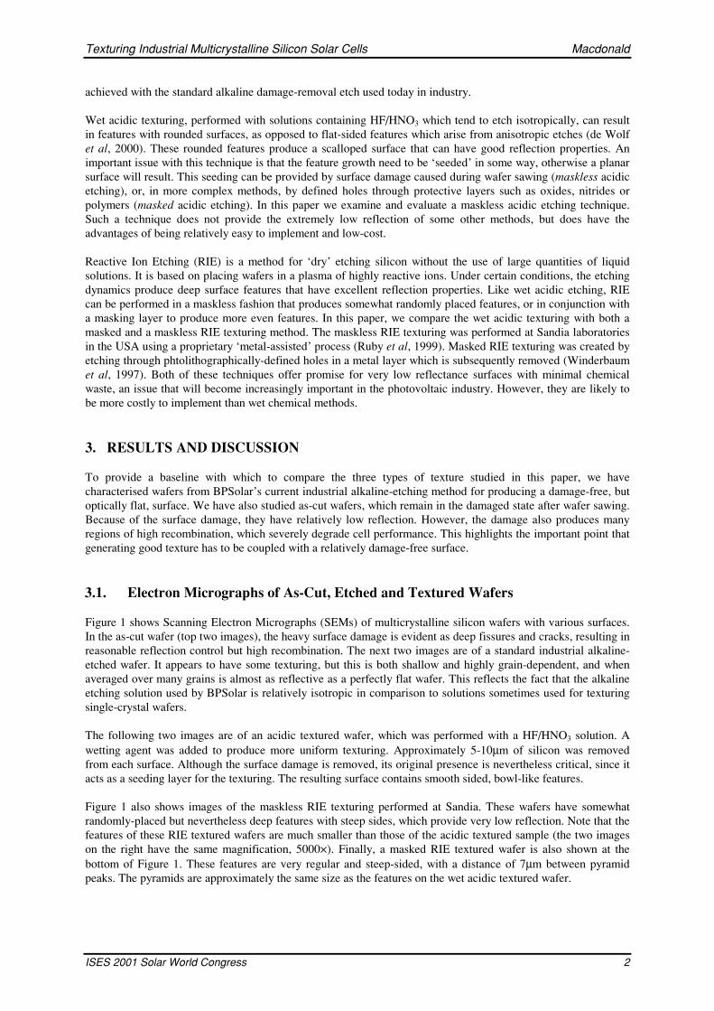
Figure 2. Reflectance measurements of bare alkaline-etched, as-cut, acidic textured, masked RIE andmaskless RIE textured multicrystalline silicon wafers.
3.2. Reflectance Measurements
Figure 2 shows the results of reflectance measurements on the three types of textured wafers, plus alkaline-etchedand as-cut samples. These curves have been used to calculate weighted reflectances for the AM1.5G spectrum.The results are shown in Table 1.
As-cut Alkalineetched
Acidictextured
MasklessRIE
Masked RIEpyramids
Bare 22.6% 34.4 27.6 11.0 5.6*With SiN AR coating 7.6 9.0 8.0 3.9 n/aSiN & encapsulated 8.9 12.9 9.2 7.6 n/a
Table 1. Weighted AM1.5 reflectivities of bare, SiN-coated and SiN-coated/encapsulated wafers withvarious surfaces. Data marked * from Winderbaum et al. 1997.
As discussed above, the alkaline etch, which is optimised for removing the saw damage, not for texturing,produces a high reflectance. In fact, for samples of this thickness (about 275µm), a perfectly polished surfacewould also produce a reflectance of around 34%. The as-cut surface exhibits reasonable reflection control, but, asshown below, is electronically unacceptable for cell production.
The acidic textured sample produced a weighted reflectance somewhat lower than the alkaline etch, but certainlynot as good as the RIE textured samples. However, this may be offset by the relative ease of implementing acidictexturing. Purely in terms of reflectance though, the results for the RIE texturing processes are very good. Itshould be noted that the reflectance of acidic textured wafers could be improved with further optimisation, asshown by De Wolf et al, 2000, who have achieved weighted reflectances on bare wafers of about 22% (asopposed to 27.6% here).
While the results of the bare wafers give a good indication of the effectiveness of the various texturing methods,in a real cell the surface will have an encapsulated antireflection coating (ARC), which will further change theoverall reflection properties. Therefore, we have measured the reflectance of the textured surfaces coated with aplasma-enhanced chemical vapour deposited (PECVD) SiN film, both before and after encapsulation. A majoradvantage of PECVD SiN films is that they also electronically passivate the surface, leading to reducedrecombination losses. Hence there are two separate issues to consider here: firstly, the optical properties of theSiN coated textured surfaces, and secondly, how well the SiN film passivates the textured surfaces. The quality ofthe surface passivation is revealed by lifetime measurements, which are presented in the next section. Firstlythough, we present reflectance results on SiN coated wafers.
0
10
20
30
40
50
60
70
80
90
100
300 400 500 600 700 800 900 1000 1100 1200
Wavelength (nm)
Ref
lect
ance
(%
)
alkaline-etched
acidic textured
as-cut
maskless RIE
masked RIE pyramids
Bare wafers
Texturing Industrial Multicrystalline Silicon Solar Cells Macdonald
ISES 2001 Solar World Congress 5
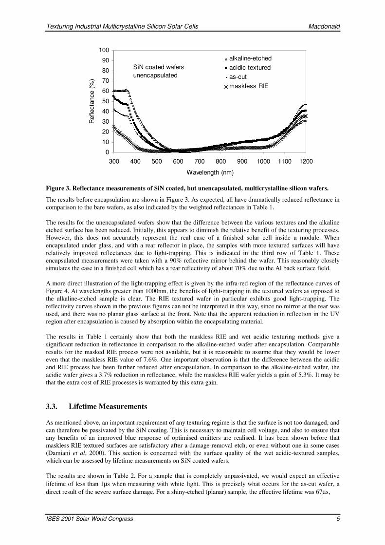
Figure 3. Reflectance measurements of SiN coated, but unencapsulated, multicrystalline silicon wafers.
The results before encapsulation are shown in Figure 3. As expected, all have dramatically reduced reflectance incomparison to the bare wafers, as also indicated by the weighted reflectances in Table 1.
The results for the unencapsulated wafers show that the difference between the various textures and the alkalineetched surface has been reduced. Initially, this appears to diminish the relative benefit of the texturing processes.However, this does not accurately represent the real case of a finished solar cell inside a module. Whenencapsulated under glass, and with a rear reflector in place, the samples with more textured surfaces will haverelatively improved reflectances due to light-trapping. This is indicated in the third row of Table 1. Theseencapsulated measurements were taken with a 90% reflective mirror behind the wafer. This reasonably closelysimulates the case in a finished cell which has a rear reflectivity of about 70% due to the Al back surface field.
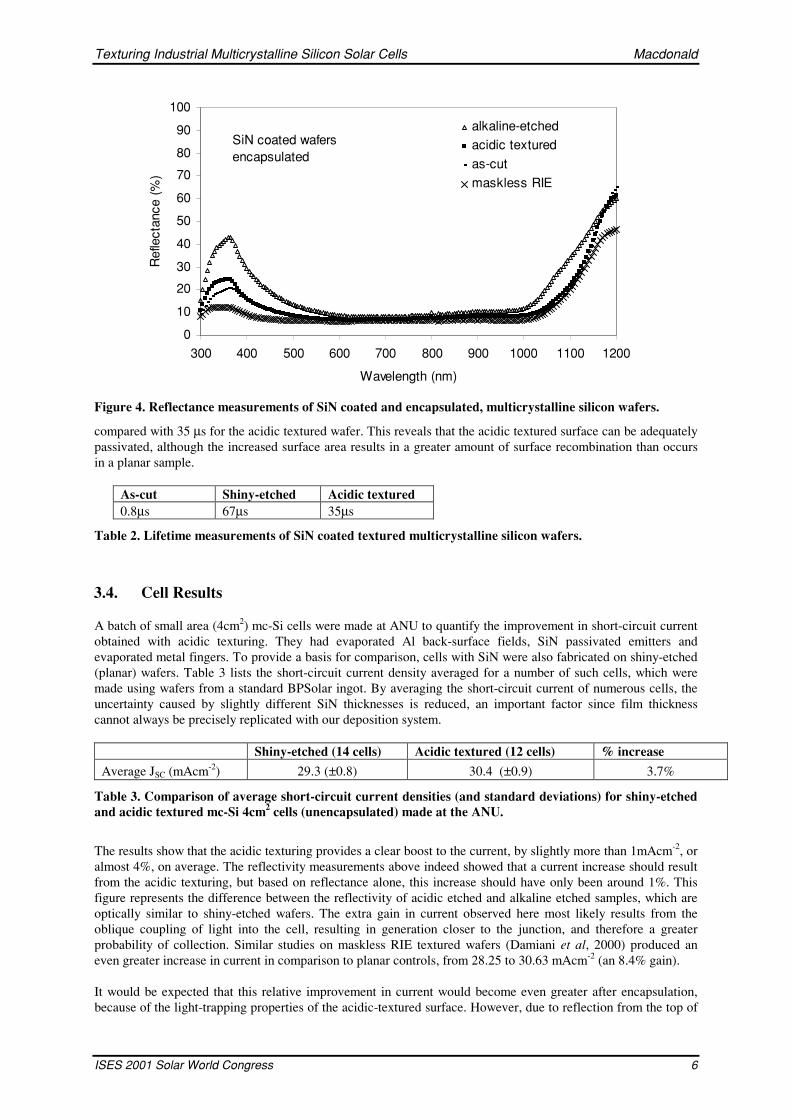
A more direct illustration of the light-trapping effect is given by the infra-red region of the reflectance curves ofFigure 4. At wavelengths greater than 1000nm, the benefits of light-trapping in the textured wafers as opposed tothe alkaline-etched sample is clear. The RIE textured wafer in particular exhibits good light-trapping. Thereflectivity curves shown in the previous figures can not be interpreted in this way, since no mirror at the rear wasused, and there was no planar glass surface at the front. Note that the apparent reduction in reflection in the UVregion after encapsulation is caused by absorption within the encapsulating material.
The results in Table 1 certainly show that both the maskless RIE and wet acidic texturing methods give asignificant reduction in reflectance in comparison to the alkaline-etched wafer after encapsulation. Comparableresults for the masked RIE process were not available, but it is reasonable to assume that they would be lowereven that the maskless RIE value of 7.6%. One important observation is that the difference between the acidicand RIE process has been further reduced after encapsulation. In comparison to the alkaline-etched wafer, theacidic wafer gives a 3.7% reduction in reflectance, while the maskless RIE wafer yields a gain of 5.3%. It may bethat the extra cost of RIE processes is warranted by this extra gain.
3.3. Lifetime Measurements
As mentioned above, an important requirement of any texturing regime is that the surface is not too damaged, andcan therefore be passivated by the SiN coating. This is necessary to maintain cell voltage, and also to ensure thatany benefits of an improved blue response of optimised emitters are realised. It has been shown before thatmaskless RIE textured surfaces are satisfactory after a damage-removal etch, or even without one in some cases(Damiani et al, 2000). This section is concerned with the surface quality of the wet acidic-textured samples,which can be assessed by lifetime measurements on SiN coated wafers.
The results are shown in Table 2. For a sample that is completely unpassivated, we would expect an effectivelifetime of less than 1µs when measuring with white light. This is precisely what occurs for the as-cut wafer, adirect result of the severe surface damage. For a shiny-etched (planar) sample, the effective lifetime was 67µs,
0
10
20
30
40
50
60
70
80
90
100
300 400 500 600 700 800 900 1000 1100 1200
Wavelength (nm)
Ref
lect
ance
(%
)
alkaline-etched
acidic textured
as-cut
maskless RIE
SiN coated wafersunencapsulated
Texturing Industrial Multicrystalline Silicon Solar Cells Macdonald
ISES 2001 Solar World Congress 6
Figure 4. Reflectance measurements of SiN coated and encapsulated, multicrystalline silicon wafers.
compared with 35 µs for the acidic textured wafer. This reveals that the acidic textured surface can be adequatelypassivated, although the increased surface area results in a greater amount of surface recombination than occursin a planar sample.
As-cut Shiny-etched Acidic textured0.8µs 67µs 35µs
Table 2. Lifetime measurements of SiN coated textured multicrystalline silicon wafers.
3.4. Cell Results
A batch of small area (4cm2) mc-Si cells were made at ANU to quantify the improvement in short-circuit currentobtained with acidic texturing. They had evaporated Al back-surface fields, SiN passivated emitters andevaporated metal fingers. To provide a basis for comparison, cells with SiN were also fabricated on shiny-etched(planar) wafers. Table 3 lists the short-circuit current density averaged for a number of such cells, which weremade using wafers from a standard BPSolar ingot. By averaging the short-circuit current of numerous cells, theuncertainty caused by slightly different SiN thicknesses is reduced, an important factor since film thicknesscannot always be precisely replicated with our deposition system.
Shiny-etched (14 cells) Acidic textured (12 cells) % increase
Average JSC (mAcm-2) 29.3 (±0.8) 30.4 (±0.9) 3.7%
Table 3. Comparison of average short-circuit current densities (and standard deviations) for shiny-etchedand acidic textured mc-Si 4cm2 cells (unencapsulated) made at the ANU.
The results show that the acidic texturing provides a clear boost to the current, by slightly more than 1mAcm-2, oralmost 4%, on average. The reflectivity measurements above indeed showed that a current increase should resultfrom the acidic texturing, but based on reflectance alone, this increase should have only been around 1%. Thisfigure represents the difference between the reflectivity of acidic etched and alkaline etched samples, which areoptically similar to shiny-etched wafers. The extra gain in current observed here most likely results from theoblique coupling of light into the cell, resulting in generation closer to the junction, and therefore a greaterprobability of collection. Similar studies on maskless RIE textured wafers (Damiani et al, 2000) produced aneven greater increase in current in comparison to planar controls, from 28.25 to 30.63 mAcm-2 (an 8.4% gain).
It would be expected that this relative improvement in current would become even greater after encapsulation,because of the light-trapping properties of the acidic-textured surface. However, due to reflection from the top of
0
10
20
30
40
50
60
70
80
90
100
300 400 500 600 700 800 900 1000 1100 1200
Wavelength (nm)
Ref
lect
ance
(%
)
alkaline-etched
acidic textured
as-cut
maskless RIE
SiN coated wafersencapsulated
Texturing Industrial Multicrystalline Silicon Solar Cells Macdonald
ISES 2001 Solar World Congress 7
the glass (about 4.5%), the magnitude of the current will in fact decrease after encapsulation for both acidictextured and planar cells, but the decrease should be less for textured cells.
Table 4 shows that this is indeed the case. It gives a comparison of the short-circuit currents of two individualmc-Si cells, one of which was acidic textured and the other shiny-etched, before and after encapsulation. Theresults show that the gain from acidic texturing increased from 3.3% to 5.1% after encapsulation (an increase of1.8%). This is similar to the results of De Wolf et al., 2000, who observed an improvement of 6.4% for a modulemade of acidic textured cells in comparison to a module of alkaline-etched cells. The results from Table 1indicate that the difference in reflectance between planar and acidic textured wafers widens from 1% to 3.7%after encapsulation. This suggests that a further 2.7% relative current gain can reasonably be expected afterencapsulation of acidic textured samples compared with planar cells, a little higher but still in reasonableagreement with the observed increase of 1.8%. Generally speaking, these results certainly show that acidictexturing provides significant gains in terms of current in BPSolar material.
Cell91DA shiny-etched 90AB acidic textured % difference
JSC before encapsulation
JSC after encapsulation
% change in JSC
30.7
29.7
-3.4%
31.7
31.2
-1.6%
3.3%
5.1%
1.8%
Table 4. Comparison of short-circuit current densities for an acidic textured and a shiny-etched SiN-coated mc-Si 4cm2 cell before and after encapsulation.
4. CONCLUSIONS
All three texturing methods examined - wet acidic texturing, and masked and maskless RIE texturing –significantly reduce reflection losses in solar cells. The reduction in reflection is greatest for masked RIEpyramids, followed by maskless RIE, and then acidic texturing, and this is likely to also be the order of greatestimprovement in cell performance. However, the relative difference between the methods is substantially reducedafter antireflection-coating and encapsulation. Also, the cost of implementation is likely to be substantially lessfor acidic texturing then for either RIE process, especially masked RIE. It is therefore difficult to accuratelyquantify, at this stage, which technique offers the best prospects for commercial implementation.
5. ACKNOWLEDGMENTS
This work has been supported by the Australian Greenhouse Office through the Renewable EnergyCommercialisation Program (RECP), and by the New South Wales Ministry of Energy through the SustainableEnergy Research and Development Fund (SERDF). The authors are grateful to James Cotsell and MickStuckings from CSES at the ANU for assisting with encapsulation and reflectance measurements.
6. REFERENCES
Damiani B., Ludemann R., Ruby D., Zaidi S. and Rohatgi A. (2000), Development of RIE-textured silicon solarcells, in Proceedings of the 28th IEEE Photovoltaic Specialists Conference, Anchorage, Alaska, 2000.
De Wolf S., Choulat P., Vazsonyi E., Einhaus R., Van Kerschaver E., De Clercq K and Szlufcik J. (2000),Towards industrial application of isotropic texturing for multi-crystalline silicon solar cells, in Proceedings of the16th European Photovoltaic Solar Energy Conference, Glasgow, U.K., 2000, pp. 1521-1523.
Ruby D., Zaidi S., Roy M. and Narayanan M. (1999), Plasma texturing of silicon solar cells, in Proceedings of the9th Workshop on the Role of Impurities and Defects in Silicon Device Processing, Colorado, USA, 1999, pp. 179-182.
Winderbaum S., Reinhold O. and Yun F. (1997), Reactive ion etching (RIE) as a method for texturingpolycrystalline silicon solar cells, Solar Energy Materials and Solar Cells, 46, 239-248.