testable cross-power domain interface (cpdi) …...testable cross-power domain interface (cpdi)...
TRANSCRIPT

�
�
�
�
�
�
�
�
5
Testable Cross-Power Domain Interface (CPDI) Circuit Designin Monolithic 3D Technology
JING XIE, The Pennsylvania State UniversityYANG DU, Qualcomm Corporation Research and DevelopmentYUAN XIE, The Pennsylvania State University
Optimizing energy consumption for electronic systems has been an important design consideration.Multipower domain design is widely used for low-power and high-performance applications. Data trans-fer between power domains needs a cross-power domain interface (CPDI). The existing level-conversionflip-flop (LCFF) structures all need dual power rails, which lead to large area and performance overhead.In this article, we propose a scanable CPDI circuit, utilizing monolithic 3D technology. This interface func-tions as a flip-flop and provides reliable data conversion from one power domain to another. It has a built-inscan feature, which makes it a testable design. Our design separates power rails in each tier, substantiallyreducing physical design complexity and area penalty. The design is implemented in a 20nm, 28nm, and45nm low-power technology. It shows a 20%–35% smaller insertion delay compared to normal designs. Thisproposed design also shows scalability and better energy consumption than previous LCFF circuits.
Categories and Subject Descriptors: B.6.1 [Logic Design]: Design Styles—Sequential circuits; B.6.2 [LogicDesign]: Reliability and Testing—Testability
General Terms: Design, Performance, Standardization
Additional Key Words and Phrases: Testability, level shifter, monolithic 3D, multipower domain, flip-flop
ACM Reference Format:Xie, J., Du, Y., and Xie, Y. 2014. Testable cross-power domain interface (CPDI) circuit design in monolithic3D technology. ACM J. Emerg. Technol. Comput. Syst. 11, 1, Article 5 (September 2014), 17 pages.DOI:http://dx.doi.org/10.1145/2629516
1. INTRODUCTION
Power consumption has become a first-order design goal in today’s high performanceand mobile applications. In mobile space, a nearly doubled annual growth of data de-mand and a mere 6-8% annual improvement of battery capacity quickly deplete theavailable battery charges. In the meantime, as technology continues scaling, more andmore transistors are packed into a smaller area, local hot spots and heat dissipationalso impose tremendous challenges to high performance logic systems, leading to the“dark silicon” dilemma [Esmaeilzadeh et al. 2012]. In the past, power consumptionproblem was tackled at architecture and system levels. More recently, however, lowpower device technologies also draw considerable attentions [Auth et al. 2012] and adevice-IC design cooptimization is making its way to IC design community [Seversonet al. 2012].
This work is supported by the National Science Foundation, under grant 0903432, grant 1017277.Authors’ addresses: J. Xie, Y. Xie, Computer Science and Engineering Department, Pennsylvania StateUniversity; Y. Du, Qualcomm Corporation Research and Development, San Diego, California, 92121.Permission to make digital or hard copies of all or part of this work for personal or classroom use is grantedwithout fee provided that copies are not made or distributed for profit or commercial advantage and thatcopies bear this notice and the full citation on the first page. Copyrights for components of this work ownedby others than ACM must be honored. Abstracting with credit is permitted. To copy otherwise, or repub-lish, to post on servers or to redistribute to lists, requires prior specific permission and/or a fee. Requestpermissions from [email protected]© 2014 ACM 1550-4832/2014/09-ART5 $15.00DOI:http://dx.doi.org/10.1145/2629516
ACM Journal on Emerging Technologies in Computing Systems, Vol. 11, No. 1, Article 5, Pub. date: September 2014.

�
�
�
�
�
�
�
�
5:2 J. Xie et al.
In SoC design, a common solution is to divide the system into different voltage do-mains. For example, at coarse level, computational logics and cache can be designedto operate at their own supply voltages. In multicore systems, multi-power-domains isrequired to facilitate dynamic voltage and frequency scaling (DVFS) for each core [Kimet al. 2008; Kulkarni et al. 2007]. Even within a design block, e.g. SRAM based cache,it becomes a major trend to have multiple power supplies [Chang et al. 2013; Pilo et al.2013]. Generally, finer granularity of voltage domains is known to reduce system powermore effectively and is considered as an attractive approach of mitigating the powerwall problem [Kikuchi et al. 2011].
Multipower-domain design requires logic level shifters at domain boundaries toassure reliable cross-domain data transfer and manage cross-domain data traffic. Sev-eral level shifter structures were published in the past [Khan et al. 2006; Tran et al.2005; Usami et al. 1998]. These level shifters are, however, area and performance inef-ficient, when connecting with flip-flop. Recently, sequential logic cell integrating levelshifting function has been proposed in master-slave flip-flop designs [Ishihara et al.2004; Lin et al. 2008]. These designs explored the possibility to minimize area penaltyand to reduce circuit delay. Practical implementation, however, needs to address thecomplexity of in-cell dual power rail physical design and the problem of voltage do-main isolation. These challenges hinder the widespread acceptance of fine-grainedmultivoltage domain system design due to considerable area penalty and additionaldesign complexity.
Fortunately, recent advance in monolithic 3D integration technology may lead toa fundamental breakthrough in reducing overhead of the multivoltage domain sys-tem design [Batude et al. 2011; Bobba et al. 2010; Mayberry 2012]. The small mono-lithic inter-tier vias (MIVs), which is similar to normal interconnect via, providehigh speed and high-density interconnection between different tiers. Implementing inmonolithic 3DIC, the in-cell dual power rails can be naturally separated and managedin different tiers, greatly simplifies the physical layout design than in conventional2D IC.
In this study, we propose a novel cross-power domain interface (CPDI) circuit, whichtransfers synchronous data between power domains effectively and reliably. Our CPDIcircuit utilizes the level conversion flip-flop (LCFF) structure, and resolves the isola-tion problem by using a differential pair of common source nMOS in the data pathbetween the master and slave stages of this LCFF design. Self-induced voltage col-lapsing (SIVC) technique [Kulkarni et al. 2012] is further introduced to enhance levelshifter efficiency and reduce conversion power. Moreover, the transistors in the levelshifting stage are sized such that it minimizes area and achieves reliable data trans-fer at the worst case process corner simultaneously. This is a practical design with thescanable feature and it scales with the technology nodes.
The proposed CPDI is implemented in a dual-tier 3DIC. Two power rails of the CPDIcircuit are readily arranged in two separate tiers. Taking the advantages of our novelcircuit topology and monolithic 3DIC implementation, we achieved a highly compact,highly reliable, low power CPDI design. Comparing with the conventional flip-flop pluslevel shifter design, our optimized CPDI shows a 20%–35% delay improvement andconsiderable dynamic energy and leakage saving.
To our knowledge, this is the first time that a practical CPDI circuit is designedand implemented in monolithic 3DIC. The implementation in 3DIC is also essentialfor cross-tier, cross-domain synchronized data transfer in future multivoltage domain3DIC systems. Later in the article, we will introduce the background knowledge inSection 2. The detailed CPDI circuit design will be provided in Section 3. We will showthe experimental results in Section 4 and conclude the work in Section 5.
ACM Journal on Emerging Technologies in Computing Systems, Vol. 11, No. 1, Article 5, Pub. date: September 2014.

�
�
�
�
�
�
�
�
Testable Cross-Power Domain Interface (CPDI) Circuit Design in Monolithic 3D Technology 5:3
Fig. 1. Circuit performance and energy relationship under different voltage for combinational logics.
Fig. 2. Dynamic, leakage and total energy per cycle.
2. MOTIVATION AND BACKGROUND
2.1. Low Power Design and Voltage Scaling
The power consumption is critical in today’s integrated circuit design. Changing thesupply voltage is an effective way to reduce power. There is an interesting trade-offbetween using low supply voltage, and thus saving the dynamic power, versus usingnormal supply voltage, which decreases the operation time. The major task is to findthe optimal design point of a circuit by means of switching energy, leakage power andperformance.
The performance and power relation is studied by using circuit level benchmarks in45nm technology. We simulated an inverter chain that could represent combinationallogics. The result shows that power consumption increases much faster than speedunder high supply voltage (Figure 1). A chip is limited by its power/thermal budgetin this region. Under low voltage, the power is minimized at the expense of rapidlydecreased performance.
Efficiency of the circuit, which is defined by the energy per operation, is another im-portant consideration. For a given computational task, we expect to use minimal en-ergy to complete it within allowed time. It is known that maximum energy efficiencyoccurs at near threshold voltage [Kaul et al. 2012]. Threshold voltage is the voltageat which the transistor is considered to the turned on. It is defined on the biggest gmpoint for long channel devices. For modern technology nodes, it is usually defined bythe Vgs when the on current is above a certain value per unit channel Width/Length. Itdepends on the process and usually multi-Vth device cells are provided in one processfor energy efficient design. For example, the 45nm process we used here has a thresh-old voltage around 0.4 V. As shown in Figure 2, the operation voltage could be divided
ACM Journal on Emerging Technologies in Computing Systems, Vol. 11, No. 1, Article 5, Pub. date: September 2014.

�
�
�
�
�
�
�
�
5:4 J. Xie et al.
Fig. 3. Monolithic 3D structure.
into three regions based on energy efficiency: the sub-Vth voltage region wasted bothenergy and performance; the middle region has the lowest energy consumption withrelatively low performance; the high voltage region has the best performance and highenergy consumption as well. Hence, it is essential and tricky to determine the opera-tion voltage for one design to meet the design constraint.
The previous discussion is about getting the optimal trade-off point for one circuitblock. However, there are many blocks in a VLSI design. Each block has its uniqueperformance-power relationship. For example, the core and the cache usually havedifferent energy efficiency under the same operation voltage. There is no single optimalsupply voltage for the whole system. Therefore, multi voltage domain design is amongthe best solution for low power design. For example, using the high supply voltage inthe timing critical critical blocks, while keeping other blocks operate at a low voltage tocontrol the leakage; using high voltage for the SRAM array for better performance andless error rate, while using low voltage for the cache decoder to reduce system power.
2.2. Monolithic 3D Technology
Monolithic 3D technology is introduced in recent years [Batude et al. 2011; Bobbaet al. 2010]. Technology scaling helps the performance of transistors. However, globalinterconnect wire delay does not scale accordingly. The increasing wire delays is oneof the major impediments for performance improvement [Xie et al. 2010] under thesame power budget. Monolithic 3D offers an opportunity to continue the performanceimprovements and power saving by reducing the interconnect distance, which makesit one of the most promising technology for circuit scaling [Lee et al. 2012].
The monolithic 3D IC is fabricated by stacking high quality mono-crystalline siliconlayers using low temperature oxide bonding, followed by low temperature transistorand interconnect integrations, sequentially. Connections between tiers are made bymonolithic intertier vias (MIVs). The process is effectively the same as fab front-endand back-end integration flow, using similar mask alignment technique and CD con-trol. This way, MIV size can be made as small as regular interconnect vias. The layoutoverhead of MIV is very small and its electrical properties can be simply modelled asa wire with parasitical RC.
MIV allows gate level inter-tier partition that will greatly changes the chip organiza-tion methodology and leads to new design challenges. Long wire delay can be reducedby folding a 2D IC design into a smaller footprint monolithic 3D stacked IC tiers.Figure 3 is the cross-sectional example of a master slave flip-flop design in monolithic3DIC. The devices on different tiers can have their own power rails. The separated
ACM Journal on Emerging Technologies in Computing Systems, Vol. 11, No. 1, Article 5, Pub. date: September 2014.
�
�
�
�
�
�
�
�
Testable Cross-Power Domain Interface (CPDI) Circuit Design in Monolithic 3D Technology 5:5
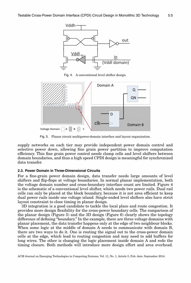
Fig. 4. A conventional level shifter design.
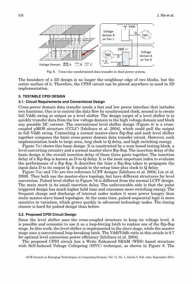
Fig. 5. Planar circuit multipower-domain interface and layout organization.
supply networks on each tier may provide independent power domain control andselective power down, allowing fine grain power partition to improve computationefficiency. This fine grain power control needs clamp cells and level shifters betweendomain boundaries, and thus a high speed CPDI design is meaningful for synchronizeddata transfer.
2.3. Power Domain in Three-Dimensional Circuits
For a fine-grain power domain design, data transfer needs large amounts of levelshifters and flip-flops at voltage boundaries. In normal planar implementation, boththe voltage domain number and cross-boundary interface count are limited. Figure 4is the schematic of a conventional level shifter, which needs two power rails. Dual railcells can only be placed at the block boundary, because it is not area efficient to keepdual power rails inside one voltage island. Single-ended level shifters also have strictlayout constraint to close timing in planar design.
3D integration is a good candidate to tackle the local place and route congestion. Itprovides more design flexibility for the cross-power boundary cells. The comparison ofthe planar design (Figure 5) and the 3D design (Figure 6) clearly shows the topologydifference of defining “boundary.” In the example, there are three voltage domains withplanar placement, the data transfer happens only at the edge of two neighbour blocks.When some logic at the middle of domain A needs to communicate with domain B,there are two ways to do it. One is routing the signal out to the cross-power domaincells at the edge, which lead to routing congestion and may need to add buffers forlong wires. The other is changing the logic placement inside domain A and redo thetiming closure. Both methods will introduce more design effort and area overhead.
ACM Journal on Emerging Technologies in Computing Systems, Vol. 11, No. 1, Article 5, Pub. date: September 2014.
�
�
�
�
�
�
�
�
5:6 J. Xie et al.
Fig. 6. Cross-tier synchronized data transfer in dual power system.
The boundary of a 3D design is no longer the neighbour edge of two blocks, but theentire surface of it. Therefore, the CPDI circuit can be placed anywhere in need in 3Dimplementation.
3. TESTABLE CPDI DESIGN
3.1. Circuit Requirements and Conventional Design
Cross-power domain data transfer needs a fast and low power interface that includestwo functions. One is to control the data flow by synchronized clock; second is to createfull Vddh swing at output as a level shifter. The design target of a level shifter is toquickly transfer data from the low voltage domain to the high voltage domain and blockany possible DC current. The conventional level shifter design (Figure 4) is a cross-coupled pMOS structure (CCLC) [Ishihara et al. 2004], which could pull the outputto full Vddh swing. Connecting a normal master-slave flip-flop and such level shiftertogether composes the basic cross-power domain data transfer circuit. However, suchimplementation leads to large area, long clock to Q delay, and high switching energy.
Figure 7(c) shows this basic design. It is constructed by a scan based testing block, alevel converting circuitry and a normal master-slave flip-flop. The insertion delay of thebasic design is the overall insertion delay of these three parts together. The insertiondelay of a flip-flop is known as D-to-Q delay. It is the most important index to evaluatethe performance of a flip flop. It describes the time a flip-flop takes to propagate theinput data D to its output Q. It equals to the setup time plus clock to Q delay.
Figure 7(a) and 7(b) are two reference LCFF designs [Ishihara et al. 2004; Lin et al.2008]. They both use the master-slave topology, but have different structures for levelconversion. Pulsed level shifter in Figure 7d is different from the normal LCFF design.The main merit is its small insertion delay. The unfavourable side is that the pulsetriggered design has much higher hold time and consumes more switching energy. Thefrequent charge and discharge of internal nodes makes it more power hungry thanstatic master-slave based topologies. At the same time, pulsed sequential logic is moresensitive to variation, which grows quickly in advanced technology nodes. The timingclosure is hard for pulsed design than before.
3.2. Proposed CPDI Circuit Design
Since the level shifter uses the cross-coupled structure to keep its voltage level, itis possible and economic to use it as a loop-forcing latch to replace one of the flip-flopstage. In this work, the level shifter is implemented in the slave stage, while the masterstage uses a conventional loop-breaking latch. The Vddl/Vddh ratio in this article is 0.7for optimal level conversion power efficiency [Ishihara et al. 2004].
The proposed CPDI circuit has a Write Enhanced SRAM (WES) based structurewith Self-Induced Voltage Collapsing (SIVC) technique, as shown in Figure 8. The
ACM Journal on Emerging Technologies in Computing Systems, Vol. 11, No. 1, Article 5, Pub. date: September 2014.

�
�
�
�
�
�
�
�
Testable Cross-Power Domain Interface (CPDI) Circuit Design in Monolithic 3D Technology 5:7
Fig. 7. Examples of cross-power boundary design and previous level convert flip-flops. (a) The master-slavehalf-latch level converter [Ishihara et al. 2004]; (b) The MSCC LCFF [Lin et al. 2008]; (c) Conventionalcross-power boundary design with a testing block; (d) The pulse latch level shifter [Karimiyan et al. 2010].
Fig. 8. Schematic of the testable cross-power boundary interface circuit.
setup/hold time of the design mainly depends on the conventional master stage, andthe clock-to-q mainly depends on the level shifting stage and the internal clock buffer.There is no DC current path between these two power domains; therefore, this voltagetripping free design has no feedback from Vddh domain to Vddl domain.
The function of the CPDI circuit is a rising edge trigger flip-flop, which has Vddl-GND range input and Vddh-GND range output. When the clock is low, the data signalgoes through the master stage T-gate. Then master stage node msnd stores the dataand msnd n stores its reverse value. N1 and N2 controlled by msnd and msnd n willpull one of their drain nodes down to ground, and make the other nMOS drain floating.The slave stage is disconnected to the master stage by two clock-controlled nMOS(N3 and N4). The output follows the data stored in the internal node of the slave stagecoupled inverters. At the rising edge, the clock turns on the slave stage nMOS N3 and
ACM Journal on Emerging Technologies in Computing Systems, Vol. 11, No. 1, Article 5, Pub. date: September 2014.

�
�
�
�
�
�
�
�
5:8 J. Xie et al.
Fig. 9. Waveform of the internal nodes when (a) Q rising and (b) Q falling.
N4. The new data goes into the slave stage and is stored at a Vddh voltage level. Forexample, if N1 and N3 are on, bit n will be written by the pull down path and bit willstore a Vddh data. During the high clock phase, the master stage T-gate is off and bothmsnd and msnd n value are maintained by the master stage clock controlled coupledinverters. Figure 9 shows the waveform of important circuit nodes.
The level shifting slave stage uses a symmetric design. The key part is similar toa SRAM cell with different customization. Normal SRAM cell needs to have balancedread/write margins. However, our design is only sensitive to the write margin andstatic noise margin when word line is closed. Therefore, we use the WES sizing tospeedup the circuit and save dynamic power. There is a dedicated port with gate con-nection for read, so that the read operation cannot disturb the internal nodes. Duringthe write operation, two clocked nMOS pass gates (N3 and N4) are turned on andthe pull down nMOS (N1 or N2) competes with the pull up pMOS. Thus, a WES designuses small device size in coupled inverters and large device size at the pull down paths.
In order to further reduce the Clk-to-Q delay and improve the pull down pathstrength, we use a minimum size always on header pMOS (P1) to increase the pullup path impedance by one stack. During level conversion, the header P1, which willcause a considerable voltage drop from Vddh to Vdd-local at the internal supply nodeS, provides the current go through both of the pMOS in the couple structure. As inFigure 9, this SIVC effect could reduce the local voltage supply level to 85%–90% ofVddh during the transition. With the technology node scaling down, this device sizemay need to be larger than the minimum size in order to guarantee speed.
Comparing with the baseline design, the new WES-SIVC structure has fewer stageson the D-to-Q path. We compromise the nMOS size on the level shifting pull downpath to achieve a better overall delay. At the same time, we use the gate connectionbetween two stages, which has two benefits. One is that by using the source/drainconnection, like the MSHL design, the master stage inverters should use much largernMOS size, because this nMOS affects the pull down time of the level shifting stage.The other benefit is removing the potential voltage tripping path. Level shifters aredesigned for low to high data converting. Nevertheless, it is quite possible that theywill transfer data from high to low voltage in real case. Under the clock is 1 situation,the source/drain connection between two stages can open a DC path through the clockcontrolled nMOS and cause the voltage tripping issue of different power domains.
The proposed design is checked at every process corner for correct function. Theworst corner of this design is the SF corner, under which the level shifting func-tion needs more margin. To assure design robustness, the proposed CPDI passed therobustness test at 10% power supply bounce.
ACM Journal on Emerging Technologies in Computing Systems, Vol. 11, No. 1, Article 5, Pub. date: September 2014.

�
�
�
�
�
�
�
�
Testable Cross-Power Domain Interface (CPDI) Circuit Design in Monolithic 3D Technology 5:9
Fig. 10. Scan chain design for multipower system. (A) the normal FF scan chain. (B) flops in each powerdomain are connected into a scan chain and the level shifter are inserted between scan chains. (C) the CPDIscan chain design that connect two opposite direction CPDI circuits one after another. (D) the CPDI scanchain design with integrated level shifting function.
3.3. The Cross-Boundary Scan Chain in 3D Circuits
Testability is essential for VLSI circuits. The scan based testing is the common testingmethod, which needs Q value to be scanned out for debugging. Thus every sequentialunits need to have scanable feature. However, the input and output signals of a CPDIcircuit are located at two voltage domains, which makes the scan chain design differentfrom the 2D cases.
3.3.1. Scan Connection Method. The normal scan chain design is connecting all the flip-flops in an area with the least P&R resource, because the influence of scan chain to thefunction blocks should be minimized. For a multipower domain system using our CPDIdesigns, the normal flip-flops and CPDI circuits can be placed together in one blockarea. In this way, sharing one scan chain is a nature and efficient way. However, theshared scan chain makes the scan data flow complex, which could change frequentlybetween two or more voltage levels. The designer has to determine where, when to addwhat kind of level shifters during the scan chain insertion for a correct function. Thetiming closure for such complex design could be messy. Moreover, the dual power raillevel shifter may consume more limited P&R resources. Thus it is meaningful to finda simple and unified scan chain design with proposed CPDI circuits.
Three methods are considered here, as illustrated in Figure 10. (A) is the normalscan chain design, in which there is only one power domain. The scan chain is formedby the location of each flip-flop and the connection consideration is to take the leastP&R resource. Method 1 in (B) is connecting all the FFs in one power domain into onechain, and using level converters to connect each group. This method could not includeany LCFF, because all the FFs inside a group only have one voltage level. It is veryhard to have a fine grain power domain partitioning by using this method, because it isnot energy and area efficient when the cross-power domain data transfer is frequent.Method 2 in (C) is connecting the CPDI circuits in a interdigital way into a scan chain.Making sure that every domain A→B LCFF is connected with a domain B→A LCFF.This method has the least chain complexity in the ideal case. For example, the cross-power domain design is between the logic and memory, the read out data and write in
ACM Journal on Emerging Technologies in Computing Systems, Vol. 11, No. 1, Article 5, Pub. date: September 2014.

�
�
�
�
�
�
�
�
5:10 J. Xie et al.
data has the same number of pins and could form one chain. The issue for this methodis obvious that it is hardly possible to find exact number of opposite directional sig-nals placed close to each other. The connection overhead and the imbalanced oppositedirectional data transfer are the critical obstacles for this method. Method 3 in (D) isa new kind of CPDI circuit that could be simply connected together with the build-inlogic level conversion function. This method has no connection constraint, so that it isthe easiest way for scan chain connection. It could be used exactly in the same way asa single power domain case.
3.3.2. CPDI Circuit Scan Chain Design. Our proposed CPDI circuit includes the scanablefeature that follows method 3. A differential input level shifter is added at the scanin data pin. It is from the Q and Q n of the previous stage in its scan chain. The scanpath speed requirements is much slower than the D-to-Q path. Thus the transistor sizeare minimized to save the area and ensure correct function at all process corner casesunder a longer cycle time. On the other hand, a short setup time need to be guaranteedafter adding the D path scan select T-gate. This T-gate on the D path controlled by SENand SEN n matches the clk controlled T-gate size.
The power of scan path is not critical, since the scan function is not used in normaloperation. The leakage of the scan path under normal operation is a major concern.To further reducing leakage, one power gating pMOS could be added on the scan path.During scan mode, this SEN controlled header is on. In normal operation, this headeris off and the whole scan path is in the power down mode.
3.4. Partition and Layout Balancing
The dual-tier CPDI logic structure shown in Figure 6 exploits monolithic 3D technol-ogy. The Vddl power island is on tier 0 and Vddh power island is on tier 1. For multi-power domain design, most of the standard cells locate in a single power domain andhave one power rail. Dual-power rail design LCFF will significantly decrease the placeand route flexibility and increase the design complexity. Our monolithic 3D based de-sign does not have this problem, because it is a single power rail design in each tier.MIVs transfer the data signal between two domains.
The partition of this CPDI circuit into tiers has two considerations: power domainisolation and cell footprint. Two tiers have separated power rails, so that transistorsconnected to different supply rails must be placed in the correspondent tier. Othertransistors, like pass gates, are placed to either tier that provides less footprint. Con-sidering the above two criteria, we partition the master stage, scan in transistors andclock buffer into tier 0, and the level shifting slave stage into tier 1. The transistorson each tier are placed such that the overall transistor widths in each tier are close tomaximize 3DIC area utilization. Thus, this design has compact layout and make fulluse of vertical interconnecting resource.
4. EXPERIMENTAL RESULTS AND COMPARISON
The performance of the proposed WES-SIVC design is compared with several other re-ported LCFF designs. All these designs are implemented in a 3D IC style that containstwo tiers of active devices. MIVs deliver the communication signals between the twotiers. An MIV has similar electrical properties as a normal via between metal layersand thus are not specially modelled in the schematic. This is different from TSV basedmultitiers designs, where the TSV capacitance is not negligible. The designs are placedacross two tiers with different power rails. The voltage level of each tie is independentof the other. The maximum voltage is chosen to be 1.1 times of the process nominalvoltage, and the minimum voltage is 70% of the maximum voltage.
ACM Journal on Emerging Technologies in Computing Systems, Vol. 11, No. 1, Article 5, Pub. date: September 2014.

�
�
�
�
�
�
�
�
Testable Cross-Power Domain Interface (CPDI) Circuit Design in Monolithic 3D Technology 5:11
Fig. 11. D-to-q of the designs under 45nm, 28nm, and 20nm process.
Scalability is an important factor in choosing the circuit design style. All the circuitsunder evaluation are implemented in 3 different technology nodes, which include a45nm bulk low power, a 28nm bulk low power and a 20nm FDSOI process [Haond2012]. The circuit performance of 6 designs is compared within each process node. Thetransistor sizes in the designs are optimized for D-to-Q delay, under the condition thatthe inputs come from the lower voltage domain and the outputs are in the high voltagedomain. Not timing critical devices are chosen to use minimum possible size that keepsthe correct circuit function.
4.1. Timing and Energy of CPDI Designs
Timing and energy of the new WES style designs are compared with the two otherLCFF structures, which are the MSHL and MSCC reported in Ishihara et al. [2004]and Lin et al. [2008]. A baseline structure in this study is constructed by a flip-flop anda separate CCLC (Figure 4). The flop is placed in the low voltage domain and CCLCshifts the flop output to the high voltage domain. Pulse design is frequently used inhigh speed circuits. A pulse latch proposed in Karimiyan et al. [2010] is implementedfor speed and energy comparison. For fair comparison, all designs follow the rule be-low in transistor sizing. The sizes are identical for the master stage of the flip-flopand the local clock drivers. The device sizes of the slave stage are slightly modified ineach design to ensure proper level shifting function. The pull-up and pull-down pathstrength at the level shifting nodes are carefully tuned to assure correct function un-der the largest input/output voltage difference in all process corners. The output stageuses a FO4 loaded inverter to mimic practical output environment. In this section, thediscussion is focused on the 45nm process node data.
The D-to-Q delay of all 6 designs are compared in Figure 11. The values are aver-aged between the output rising/falling cases. The insertion delay of the WES-SIVC issimilar to the one without the SIVC structure. The header pMOS weaken the slavestage pull-up strength during state transition, and thus speed up the internal bit/bit nnode falling transition by 20%. The output Q rising transition is faster since the inter-nal bit n node is pulled down quickly. On the other hand, the Q falling case does notbenefit much from the header pMOS. Bit node has the 1 → 0 transition before bit nhas 0 → 1 transition, while the temporary drop of VDD limits the bit n rising speed.These two WES type designs are the fastest master-slave LCFF in all designs. TheMSHL structure has slightly longer (6%) insertion delay than the WES type flops. Thebaseline FF+LC structure has 60% larger delay. The pulse latch design insertion delayis only 35% of the baseline because of its negative setup time, but it consumes a lot ofpower and has long hold time.
Temperature sensitivity is important for both level shifter designs and 3D ICs. Theproposed design shows very similar temperature sensitivity to the baseline design inFigure 12 in reference to the D-to-Q delay. The experiment is of the 28nm node. Thistrend meets the design expectation, because the temperature sensitivity can be dividedinto the setup part and the Clk-to-Q part. The setup delay mainly depends on the path
ACM Journal on Emerging Technologies in Computing Systems, Vol. 11, No. 1, Article 5, Pub. date: September 2014.

�
�
�
�
�
�
�
�
5:12 J. Xie et al.
Fig. 12. Design sensitivity comparison to temperature.
Fig. 13. Switching energy of the designs under 45nm, 28nm, and 20nm process.
in the low power domain, while the C-to-Q delay mainly depends on the path in thehigh voltage domain. The WES-SIVC has shorter path in the high domain. Thus theClk-to-Q delay variation of WES-SIVC is significantly lower than the baseline design,but the WES-SIVC design has longer setup time than the Clk-to-Q delay, which makesthe overall D-to-Q delay temperature sensitivity difference negligible. One interest-ing thing worth to be mentioned here is that both circuits shows better performanceat higher operation temperature, which is result of the reverse temperature effect atadvanced technology nodes.
Energy consumption for the 6 designs are compared in Figure 13. The data is calcu-lated as the average energy for both output rising and falling cases at a clock periodof 2 ns and a data activity of 50%. It includes the total energy consumption at Vddland Vddh voltage domains and also the leakage energy during the clock period of bothdomains. Energy is calculated with the following equation.
Etotal =∫ 2ns
0(Vddhigh · Ihigh + Vddlow · Ilow)dt. (1)
The energy of the WES-SIVC design is 92% of the same structure w/o SIVC. TheFF+LC design consumes less energy than the MSCC structure, but it is still worsethan the WES style structures. The pulse latch design has the largest energy due tothe high switching activity in the pulse generator. Comparing the leakage power inFigure 14, the WES w/o SIVC design has the same leakage as the one with SIVC ver-sion, because the always on pMOS does not affect the leakage current. All the LCFFstructures contain fewer single stacking transistors comparing with the FF+LC de-sign, thus their leakage power is greatly reduced. This makes LCFFs style designpreferable in advanced technology nodes, where the leakage power occupies a largepercentage of total power.
The energy delay product (EDP) of the 6 designs is compared in Figure 15. TheWES-SIVC structures achieves 50% EDP of the baseline design. The use of SRAMtype structure with SIVC effect greatly improves the slave stage from previous LCFF
ACM Journal on Emerging Technologies in Computing Systems, Vol. 11, No. 1, Article 5, Pub. date: September 2014.

�
�
�
�
�
�
�
�
Testable Cross-Power Domain Interface (CPDI) Circuit Design in Monolithic 3D Technology 5:13
Fig. 14. Leakage of the designs under 45nm, 28nm, and 20nm process.
Fig. 15. Energy delay product of the designs under 45nm, 28nm and 20nm process.
Table I. Data Comparison for Timing, Energy, EDP and Area of the Six Designs
Timing Energy EDP AREAD to Q Dynamic Energy Leakeage
45nm 28nm 20nm 45nm 28nm 20nm 45nm 28nm 20nm 45nm 28nm 20nmWES-SIVC 0.61 0.77 0.80 0.82 1.02 0.79 0.69 0.65 0.67 0.50 0.78 0.63 18
WES 0.61 0.78 0.79 0.87 1.10 0.82 0.69 0.65 0.67 0.53 0.85 0.65 18MSHL 0.65 0.84 0.91 0.87 1.09 0.80 0.78 0.76 0.73 0.56 0.92 0.73 18MSCC 0.87 1.12 1.07 1.24 1.44 1.32 0.88 0.82 0.82 1.07 1.62 1.41 20FF+LC 1.00 1.00 1.00 1.00 1.00 1.00 1.00 1.00 1.00 1.00 1.00 1.00 20Pulse 0.33 0.43 0.60 1.24 2.09 1.75 1.35 1.09 1.09 0.57 0.91 1.05 16
* Data is normalized to the FF+LC baseline structure. Area is counted by tracks.
designs and also reduces the interference between the two stages. Although the pulselatch design has short insertion delay, its EDP is not superior to the WES style de-signs. The area of these designs are listed in Table I. The circuit layouts are designedfor standard cell style P&R, whose area are counted by poly tracks. The footprint ofthe new WES type designs utilizing monolithic 3DIC is 8 and 10 tracks on each tier.The total chip area of these two layers is 18 tracks, which has the same area as theMSHL design. They uses 90% of the conventional FF+LC design area. Table I alsosummarizes the normalized timing, energy and EDP data discussed above.
The setup and hold constraints are compared in Figure 16. Setup time is measuredfrom D-to-clock, hold time is measured from clock-to-D. They are measured by theclock-to-q push out method. A negative setup time indicates that the constraint isafter the clock edge, a negative hold time indicates that it is before the clock edge. Thehold time bars in the plot use a reversed vertical axis, so that the height differencebetween the setup and hold bars show the length of the timing window that datacannot change. This difference is shown as the gray area in each bar. The WES-SIVCstructure has the best setup/hold time among all master-slave LCFFs, but it is worsethan the conventional FF+LC design. The level shifting function in the slave stagerequires the data to be ready earlier and hold for a longer time. In the MSHL design,the master stage involves in the level shifting fighting, the interaction leads to a larger
ACM Journal on Emerging Technologies in Computing Systems, Vol. 11, No. 1, Article 5, Pub. date: September 2014.

�
�
�
�
�
�
�
�
5:14 J. Xie et al.
Fig. 16. Setup time, hold time of the designs under 45nm, 28nm and 20nm process.
Table II. Scan Path Timing Constraints
EnergySetup Time (ps) Hold time (ps)
45nm 28nm 20nm 45nm 28nm 20nmWES-SIVC 533.3 270.0 71.0 −341.9 −150.6 −53.7
WES 543.9 276.8 71.3 −336.5 −146.6 −52.6MSHL 595.0 305.0 82.3 −313.6 −126.2 −50.1MSCC 629.7 311.7 64.9 −93.4 −56.1 −42.9FF+LC 162.4 115.8 24.4 −67.4 −47.4 −20.3Pulse −87.3 −71.9 −42.7 400.3 171.5 73.2
setup/hold time. The WES style designs isolate the two stages in a LCFF, and thushas better constraint requirement comparing to the other LCFF designs. ApplyingSIVC technique improves the slave stage bit/bit n nodes transition speed, which makesconstraint timing window smaller.
The scan path timing constrains are listed in Table II. The setup time of the SIN pinis longer than the D pin setup. It means the scan-in data need to be ready earlier thanthe D pin data. This constraint is not tight for scan path, because the scan frequency isusually much less than the flip-flop normal operation frequency. The hold time of SINpin is smaller than the Clk to Q, such that there is no need to add additional buffersin the scan chain for correct function. In this scan path, our design still shows bettersetup/hold time than all the other LCFF designs. In this way, this scan based CPDIdesign is practical.
4.2. Scaling of CPDI Designs
Scalability is an important aspect of digital circuit IPs. The performance and powerconsumption of a good LCFF design should always be better than the FF+LC struc-ture with the evolution of technology nodes. The 6 CPDI structures discussed in theprevious section are implemented in three tech nodes for scalability comparison. Thecircuits are ported from the 45nm tech node to the other two nodes, while the areais shrunken proportionally to the square root of the channel length ratio. After port-ing, the device sizes within a circuit topology are tuned based on the specific p/n MOSstrength ratio. The level shifting function is checked at the worst PVT corner again af-ter porting to ensure correct operation at a target frequency. The circuit performanceis evaluated with the same method, while the input drivers and output loading areshrunken among tech nodes.
The D-to-Q delay of the 3 tech nodes are shown in Figure 11. For each design, the in-sertion delay shrinks with tech nodes. The WES-SIVC delay at 20nm FDSOI is 80% ofthe 45nm LP process. The WES style and the MSHL designs always have smaller de-lay than the FF+LC design, but the MSCC has longer delay than the FF+LC structure
ACM Journal on Emerging Technologies in Computing Systems, Vol. 11, No. 1, Article 5, Pub. date: September 2014.

�
�
�
�
�
�
�
�
Testable Cross-Power Domain Interface (CPDI) Circuit Design in Monolithic 3D Technology 5:15
Table III. S Node VoltageDrop Percentage Relative
to Vdd
45nm 28nm 20nm8.3% 13.4% 12.0%
at the 28nm process. The delay of circuits shrinks with advanced technology nodes.However, the designs with voltage tripping issue does not benefit from the scalingas much as other structures, because of the N/P driving strength change. The MSCCstructure has the most severe voltage tripping problem. The baseline design and ourproposed designs do not suffer from the same issue. Thus FF+LC shows a better per-formance over MSCC design in advanced technology nodes. Comparing among the de-signs within a tech node, the difference is large at 45nm and 28nm nodes. The delayvalues become close to each other at the 20nm FDSOI node, because a single stage de-lay at this process is very short, therefore, a few more stages of inverters do not causesignificant difference. If the 20nm tech node is implemented in bulk CMOS, the delaydifference among these circuits is expected to become larger.
It is possible that the node S voltage drop level changes with the technology nodes.The result of this temporary voltage drop is listed in Table III. There is a 8.3% to13.4% voltage drop. Thus the minimum size pMOS header is big enough under thesetech nodes.
The energy of the LCFF designs also shrinks at smaller tech nodes (Figure 13). Theenergy is mainly contributed by charging/discharging the gate cap and the DC currentduring level shifting. The gate cap is smaller at advanced tech nodes. The energy causeby DC current is reduced due to shorter transition time during level shifting, and thusthe total energy is smaller. The energy of the pulse design does not shrink from 45nmto 28nm design, which is from the large energy consumption at the pulse generator.The EDP value at the three tech nodes are shown in Figure 15. The WES style and theMSHL designs always have better EDP than the baseline at all 3 tech nodes, but thegap becomes smaller at advanced tech nodes. The ratio of EDP between WES-SIVCand baseline designs is around 0.5–0.8, depending on device sizing and technologyrelated device character. The sizing method in this study is optimized for D-to-Q delay,and thus we observe this EDP ratio fluctuates among tech nodes. The pulse designdoes not scaling well with the evolution of technologies. Its EDP becomes larger thanthe baseline at 20nm node.
The constraint time at the three tech nodes are compared in Figure 16. The setuptime reduced from 194 ps in 45nm to 39 ps in 20nm FDSOI process for the WES-SIVCdesign. The data changing forbidden window is also reduced from 96 ps to 9 ps. At allthree tech nodes, the WES style designs have similar setup/hold characteristic as thenormal FF and are scaled under the same trend. However, the WES style design setupvalue is larger because of the influence of the level shifting function.
5. CONCLUSION
In this work, we proposed a scanable design of cross-power domain interface for datatransfer. We evaluated it under different flavor process and technology nodes. This in-terface is constructed by a Master-Slave flip-flop followed by a level shifter functionedas its slave stage. The level shifter uses the 6T SRAM structure, with special size op-timization for write operation. A Self-Induced Voltage Collapse technique is applied tofurther improve performance and reducing switching power. Comparing with the base-line design, our CPDI improves both the performance and the energy consumptionby 20-35% under 10% smaller area and a 30% lower leakage. The implement of our
ACM Journal on Emerging Technologies in Computing Systems, Vol. 11, No. 1, Article 5, Pub. date: September 2014.

�
�
�
�
�
�
�
�
5:16 J. Xie et al.
design utilizes the monolithic 3D technology, which not only provides the low overheadsingle power rail structure on each tier, but also increases the flexibility of multipowerdomain design. We evaluate the influence of technology scaling for the CPDI circuit,which shows better scalability comparing with previous LCFF designs.
REFERENCES
C. Auth, C. Allen, A. Blattner, et al. 2012. A 22nm high performance and low-power CMOS technologyfeaturing fully-depleted tri-gate transistors, self-aligned contacts and high density MIM capacitors. InProceedings of the Symposium on VLSI Technology. 131–132.
P. Batude, M. Vinet, B. Previtali, et al. 2011. Advances, challenges and opportunities in 3D CMOS sequentialintegration. In Proceedings of the IEEE International Electron Devices Meeting. 7.3.1–7.3.4.
S. Bobba, A. Chakraborty, O. Thomas, P. Batude, V. F. Pavlidis, and G. De Micheli. 2010. Performance anal-ysis of 3-D monolithic integrated circuits. In Proceedings of the IEEE International 3D Systems Integra-tion Conference. 1–4.
J. Chang, Y. H. Chen, H. Cheng, et al. 2013. A 20nm 112Mb SRAM in High-metal-gate with assist cir-cuitry for low-leakage and low-VMIN applications. In Proceedings of the IEEE International Solid-StateCircuits Conference. 316–317.
H. Esmaeilzadeh, E. Blem, R. St. Amant, K. Sankaralingam, and D. Burger. 2012. Dark silicon and the endof multicore scaling. IEEE Micro 32, 3, 122–134.
M. Haond. 2012. 20 nm FDSOI process and design platforms for high performance/ low power systems onchip. In Proceedings of the IEEE International SOI Conference. 1–2.
F. Ishihara, F. Sheikh, and B. Nikolic. 2004. Level conversion for dual-supply systems. IEEE Trans. VLSISyst. 12, 2, 185–195.
H. Karimiyan, S. M. Sayedi, and H. Saidi. 2010. Low-power dual-edge triggered state-retention scan flip-flop.IET Comput. Digital Tech. 4, 5, 410–419.
H. Kaul, M. Anders, S. Hsu, A. Agarwal, R. Krishnamurthy, and S. Borkar. 2012. Near-threshold voltage(NTV) design: Opportunities and challenges. In Proceedings of the 49th ACM/EDAC/IEEE DesignAutomation Conference. 1149–1154.
Q. A. Khan, S. K. Wadhwa, and Kulbhushan Misri. 2006. A single supply level shifter for multi-voltagesystems. In Proceedings of the 19th International Conference on VLSI Design held jointly with the 5thInternational Conference on Embedded Systems and Design.DOI:http://dx.doi.org/10.1109/VLSID.2006.24.
Y. Kikuchi, M. Takahashi, T. Maeda, et al. 2011. A 40 nm 222 mW H.264 full-HD decoding, 25 powerdomains, 14-core application processor with x512b stacked DRAM. IEEE J. Solid-State Circuits 46,1, 32–41.
Wonyoung Kim, M. S. Gupta, Gu-Yeon Wei, et al. 2008. System level analysis of fast, per-core DVFSusing on-chip switching regulators. In Proceedings of the IEEE 14th International Symposium on HighPerformance Computer Architecture. 123–134.
J. Kulkarni, B. Geuskens, T. Karnik, M. Khellah, J. Tschanz, J., and V. De. 2012. Capacitive-coupling word-line boosting with self-induced VCC collapse for write VMIN reduction in 22-nm 8T SRAM. In Proceed-ings of the IEEE International Solid-State Circuits Conference. 234–236.
S. Kulkarni, A. Srivastava, D. Sylvester, and D. Blaauw. 2007. Power optimization using multi-ple supply voltages. In Closing the Power Gap Between ASIC & Custom, Springer, 189–217.DOI:http://dx.doi.org/10.1007/978-0-387-68953-1 8.
Y. J. Lee, P. Morrow, and S. K. Lim. 2012. Ultra high density logic designs using transistor-level monolithic3D integration. In Proceedings of the IEEE/ACM International Conference on Computer-Aided Design.539– 546.
Saihua Lin, Huazhong Yang, and Rong Luo. 2008. A new family of sequential elements with built-in softerror tolerance for dual-VDD systems. IEEE Trans. VLSI Syst. 16, 10, 1372–1384.
M. Mayberry. 2012. Peering through the technology scaling fog. In Proceedings of the Symposium on VLSITechnology. 1–4.
H. Pilo, C. A. Adams, I. Arsovski, et al. 2013. A 64Mb SRAM in 22nm SOI technology featuring fine-granularity power gating and low-energy power-supply-partition techniques for 37% leakage reduc-tion.In Proceedings of the IEEE International Solid-State Circuits Conference. 322–323.
M. Severson, K. Yuen, and Yang Du. 2012. Not so fast my friend: Is near-threshold computing the answer forpower reduction of wireless devices? In Proceedings of the 49th ACM/EDAC/IEEE Design AutomationConference. 1160–1162.
ACM Journal on Emerging Technologies in Computing Systems, Vol. 11, No. 1, Article 5, Pub. date: September 2014.

�
�
�
�
�
�
�
�
Testable Cross-Power Domain Interface (CPDI) Circuit Design in Monolithic 3D Technology 5:17
C. Q. Tran, H. Kawaguchi, and T. Sakurai. 2005. Low-power high-speed level shifter design for block-leveldynamic voltage scaling environment. In Proceedings of the International Conference on IntegratedCircuit Design and Technology. 229–232.
K. Usami, M. Igarashi, F. Minami, T. Ishikawa, M. Kanzawa, M. Ichida, and K. Nogami. 1998. Automatedlow-power technique exploiting multiple supply voltages applied to a media processor. IEEE J. Solid-State Circuits 33, 3, 463–472.
J. Xie, J. Zhao, X. Dong, and Y. Xie. 2010. Architectural benefits and design challenges for three-dimensionalintegrated circuits. In Proceedings of the IEEE Asia Pacific Conference on Circuits and Systems.540–543.
Received August 2013; revised December 2013; accepted January 2014
ACM Journal on Emerging Technologies in Computing Systems, Vol. 11, No. 1, Article 5, Pub. date: September 2014.