test point insertion to improve bist performance, and to...
TRANSCRIPT
Test Point Insertion to improve BIST performance,and to reduce ATPG test time and data volume

Test Point Insertion to improve BIST performance,and to reduce ATPG test time and data volume
Proefschrift
ter verkrijging van de graad van doctoraan de Technische Universiteit Delft,
op gezag van de Rector Magnificus prof.dr.ir. J.T. Fokkema,voorzitter van het College voor Promoties,
in het openbaar te verdedigen
op maandag 19 mei 2003 om 16:00 uur
door
Marc Jeroen GEUZEBROEK
elektrotechnisch ingenieurgeboren te Rotterdam

Dit proefschrift is goedgekeurd door de promotor:
Prof. dr. ir. A.J. van de Goor
Samenstelling promotiecommissie:
Rector Magnificus, voorzitter Technische Universiteit DelftProf. dr. ir. A.J. van de Goor, promotor Technische Universiteit DelftProf. dr. ir. L.K. Nanver Technische Universiteit DelftProf. ir. M.T.M. Segers Technische Universiteit EindhovenProf. dr. H. Corporaal Technische Universiteit EindhovenProf. dr. ir. Th.Krol Universiteit TwenteDr. ir. H.G. Kerkhoff Universiteit TwenteDr. ir. H.P.E. Vranken Philips Research, EindhovenProf. dr. C.I.M. Beenakker, reservelid Technische Universiteit Delft
This work has been supported and funded by Philips Semiconductors
Published and distributed by: DUP Science
Delft University PressP.O. Box 982600 MG DelftThe NetherlandsTelephone: +31 15 27 85 678Telefax: + 31 15 27 85 706E-mail: [email protected]
ISBN 90-407-2412-1
Keywords: Digital systems testing, ATPG, BIST, TPI
Copyright c© 2003 by Jeroen Geuzebroek
All rights reserved. No part of the material protected by this copyright notice may bereproduced or utilized in any form or by any means, electronic or mechanical, includingphotocopying, recording or by any information storage and retrieval system, without writ-ten permission from the publisher: Delft University Press
Printed in The Netherlands
Contents
Abstract ix
Preface and acknowledgments xi
1 Introduction 11.1 Fault models . . . . . . . . . . . . . . . . . . . . . . . . . . . . . . . . . 31.2 Testing methods . . . . . . . . . . . . . . . . . . . . . . . . . . . . . . . 5
1.2.1 Off-chip testing . . . . . . . . . . . . . . . . . . . . . . . . . . . 51.2.2 On-chip testing . . . . . . . . . . . . . . . . . . . . . . . . . . . 61.2.3 Advantages and disadvantages of off-chip and on-chip testing . . 6
1.3 Test Point Insertion . . . . . . . . . . . . . . . . . . . . . . . . . . . . . 81.4 Industrial circuits . . . . . . . . . . . . . . . . . . . . . . . . . . . . . . 8
1.4.1 The ’floating’ (Z) and ’unknown’ (U) value in three-state circuits 91.4.2 Three-state elements . . . . . . . . . . . . . . . . . . . . . . . . 10
1.5 Open questions and problems . . . . . . . . . . . . . . . . . . . . . . . . 111.6 Overview of this dissertation . . . . . . . . . . . . . . . . . . . . . . . . 12
2 Built-In Self-Test 152.1 Concept and purpose of BIST . . . . . . . . . . . . . . . . . . . . . . . . 152.2 TPG and ORA . . . . . . . . . . . . . . . . . . . . . . . . . . . . . . . . 16
2.2.1 Linear Feedback Shift Register (LFSR) . . . . . . . . . . . . . . 162.2.2 Multiple Input Shift Register (MISR) . . . . . . . . . . . . . . . 18
2.3 BIST and real-world circuits . . . . . . . . . . . . . . . . . . . . . . . . 192.4 BIST implementations . . . . . . . . . . . . . . . . . . . . . . . . . . . 20
2.4.1 Exhaustive test pattern generator (XTPG) . . . . . . . . . . . . . 212.4.2 Pseudo random test pattern generator (PRTPG) . . . . . . . . . . 222.4.3 Deterministic test pattern generator (DTPG) . . . . . . . . . . . . 242.4.4 BIST facilitation techniques . . . . . . . . . . . . . . . . . . . . 24
2.5 BIST facilitation techniques: Modify the test patterns . . . . . . . . . . . 262.5.1 Reseeding of the LFSR . . . . . . . . . . . . . . . . . . . . . . . 262.5.2 Weighted Random TPG . . . . . . . . . . . . . . . . . . . . . . 272.5.3 Mapping logic to replace useless patterns . . . . . . . . . . . . . 29
v

vi CONTENTS
2.5.4 Comparison of test pattern mutation techniques . . . . . . . . . . 312.6 BIST facilitation techniques: Fully embedded deterministic test patterns . 32
2.6.1 The pre-stored test BIST method . . . . . . . . . . . . . . . . . . 322.6.2 The LFSROM architecture . . . . . . . . . . . . . . . . . . . . . 342.6.3 The deterministic LFSR . . . . . . . . . . . . . . . . . . . . . . 35
2.7 BIST facilitation techniques: Partially embedded deterministic test patterns 382.7.1 Mapping logic . . . . . . . . . . . . . . . . . . . . . . . . . . . 382.7.2 Fixed-biased PR BIST . . . . . . . . . . . . . . . . . . . . . . . 412.7.3 Bit-flipping BIST . . . . . . . . . . . . . . . . . . . . . . . . . . 44
2.8 BIST facilitation techniques: circuit mutation . . . . . . . . . . . . . . . 472.8.1 Circuit mutation: Redesigning the circuit . . . . . . . . . . . . . 472.8.2 Circuit mutation: Inserting test points . . . . . . . . . . . . . . . 47
2.9 Summary and conclusions . . . . . . . . . . . . . . . . . . . . . . . . . 48
3 Test Point Insertion 493.1 Test points . . . . . . . . . . . . . . . . . . . . . . . . . . . . . . . . . . 493.2 TPI to facilitate testing . . . . . . . . . . . . . . . . . . . . . . . . . . . 523.3 Test point selection . . . . . . . . . . . . . . . . . . . . . . . . . . . . . 533.4 TPI for industrial circuits . . . . . . . . . . . . . . . . . . . . . . . . . . 553.5 Controllability/Observability Program (COP) . . . . . . . . . . . . . . . 55
3.5.1 Introduction to COP . . . . . . . . . . . . . . . . . . . . . . . . 553.5.2 Calculation of the COP controllability and observability . . . . . 563.5.3 Cost function and the cost gradient values . . . . . . . . . . . . . 59
3.6 STUMPS . . . . . . . . . . . . . . . . . . . . . . . . . . . . . . . . . . 633.6.1 Introduction to STUMPS . . . . . . . . . . . . . . . . . . . . . . 633.6.2 Restrictions and problems of STUMPS BIST . . . . . . . . . . . 64
3.7 State-of-the-art TPI algorithms . . . . . . . . . . . . . . . . . . . . . . . 663.7.1 The Cost Reduction Factor (CRF) TPI algorithm . . . . . . . . . 663.7.2 The Hybrid Cost Reduction Factor (HCRF) TPI algorithm . . . . 713.7.3 Multi-phase Test Point Insertion . . . . . . . . . . . . . . . . . . 783.7.4 Other state-of-the-art TPI algorithm . . . . . . . . . . . . . . . . 85
3.8 Overview TPI topics in this dissertation . . . . . . . . . . . . . . . . . . 863.8.1 TPI topics overview . . . . . . . . . . . . . . . . . . . . . . . . 863.8.2 TPI benchmark circuits . . . . . . . . . . . . . . . . . . . . . . . 87
3.9 Summary and conclusions . . . . . . . . . . . . . . . . . . . . . . . . . 88
4 Test Point Insertion for BIST 894.1 Comparison of the CRF, HCRF and MTPI algorithm . . . . . . . . . . . 89
4.1.1 Comparison of the TPI experimental results . . . . . . . . . . . . 894.1.2 Summary of the CRF, HCRF and MTPI algorithms . . . . . . . . 914.1.3 Implications of Z and U values on TPI and BIST . . . . . . . . . 93
4.2 COP for industrial circuits . . . . . . . . . . . . . . . . . . . . . . . . . 944.2.1 COP controllabilities in industrial circuits . . . . . . . . . . . . . 94
CONTENTS vii
4.2.2 COP observabilities in industrial circuits . . . . . . . . . . . . . 964.2.3 COP detection probabilities in industrial circuits . . . . . . . . . 984.2.4 The cost gradients equations in industrial circuits . . . . . . . . . 98
4.3 Proposed TPI for BIST algorithm for industrial circuits . . . . . . . . . . 1004.3.1 The Hybrid CRF TPI algorithm for industrial circuits . . . . . . . 1014.3.2 Experimental results of the Hybrid CRF TPI algorithm for indus-
trial circuits . . . . . . . . . . . . . . . . . . . . . . . . . . . . . 1044.3.3 New cost function for TPI for BIST . . . . . . . . . . . . . . . . 1074.3.4 CPU time reduction: Reduce the number of TP candidates . . . . 110
4.4 Summary and conclusions . . . . . . . . . . . . . . . . . . . . . . . . . 113
5 Test Point Insertion for compact SAF ATPG 1155.1 Impact of TPI for BIST on ATPG test set sizes . . . . . . . . . . . . . . . 1165.2 Testability analysis measures for detecting specific ATPG/test set size
problems . . . . . . . . . . . . . . . . . . . . . . . . . . . . . . . . . . 1195.2.1 SCOAP . . . . . . . . . . . . . . . . . . . . . . . . . . . . . . . 1205.2.2 Test counts . . . . . . . . . . . . . . . . . . . . . . . . . . . . . 120
5.3 Test counts in a TPI cost function . . . . . . . . . . . . . . . . . . . . . . 1245.3.1 TC and COP based cost function . . . . . . . . . . . . . . . . . . 1255.3.2 Implications of a TC based CF on the TPI algorithm . . . . . . . 1275.3.3 Results of HCRF TPI with TC based cost function . . . . . . . . 132
5.4 TPI and circuits with large Fan-out Free Regions . . . . . . . . . . . . . 1355.4.1 Four TPI techniques for reducing large FFRs . . . . . . . . . . . 1375.4.2 Experimental results of TPI for reducing large FFRs techniques . 138
5.5 Multi-stage TPI with dynamic cost function selection . . . . . . . . . . . 1405.5.1 The cost function selection procedure . . . . . . . . . . . . . . . 1405.5.2 Experimental results of multi-stage TPI . . . . . . . . . . . . . . 145
5.6 Summary and conclusions . . . . . . . . . . . . . . . . . . . . . . . . . 148
6 Test Point Insertion for delay fault ATPG 1516.1 Transition faults and gate-delay fault ATPG . . . . . . . . . . . . . . . . 1516.2 Experimental results of TPI for SAF ATPG on gate-delay fault ATPG . . 153
6.2.1 The impact of TPI for SAF ATPG on GDF ATPG in general . . . 1536.2.2 The impact of TPI for SAF ATPG on GDF test set sizes only . . . 157
6.3 Summary and conclusions . . . . . . . . . . . . . . . . . . . . . . . . . 161
7 Summary and conclusions 1637.1 Major contributions . . . . . . . . . . . . . . . . . . . . . . . . . . . . . 1677.2 Suggested topics for future research . . . . . . . . . . . . . . . . . . . . 169
A ISCAS ’85 and ’89 benchmark circuits 171
B Industrial benchmark circuits 175

viii CONTENTS
C Boolean elements 179
D Three-state elements 181
E Delft Advanced Test (DAT) generation system and AMSAL 187
Glossary 189
Bibliography 193
Samenvatting (Summary in Dutch) 201
Curriculum Vitae 203
Abstract
Test Point Insertion to improve BIST performance,and to reduce ATPG test time and data volume
The main subject of this dissertation is to facilitate structural testing by means of TestPoint Insertion (TPI) for both on-chip and off-chip tests.
Efficient production testing is frequently hampered because current complex digitaldesigns require too large test sets, even with powerful ATPG tools that generate compacttest sets. An alternative is Built-In Self-Test (BIST); by embedding the test on-chip, ex-pensive test equipment costs and test time can be reduced. However, BIST approachesoften suffer from fault coverage problems, due to random pattern resistant faults. Theseproblems can successfully be reduced, or even eliminated, by means of Test Point Inser-tion (TPI). In this dissertation we analyze three state-of-the-art TPI methods on their faultcoverage improvement for BIST and develop a novel TPI algorithm that results in evenbetter fault coverage improvement. This novel TPI algorithm has not only been developedto be applicable to Boolean circuits, but also to three-state designs. Results of several IS-CAS and Philips industrial benchmark circuits show that the proposed TPI algorithm isapplicable to both small Boolean circuits as well as to large complex industrial designs.
TPI for BIST not only improves PR fault coverage; it will be shown that TPI alsoresults in more compact ATPG test set sizes. In this dissertation new TPI methods arepresented that are aimed at solving ATPG specific testability problems, such that theATPG test set sizes and CPU times can be reduced much further. These TPI methodsare not only applicable to SAF ATPG; it has been demonstrated that also for gate-delayfault ATPG significant ATPG test set size reduction, ATPG fault coverage improvementand ATPG CPU time reduction can be achieved.
The new TPI methods have been implemented as part of the Delft Advanced TestGeneration System and AMSAL, and are currently being used within Philips as part oftheir logic test tool set.
ix

x Abstract

Preface and acknowledgments
This research on facilitating testing started in 1996 during my masters project at theComputer Engineering (CE) group of the department of Information Technology and Sys-tems at the Delft University of Technology. Because integrated circuits can contain moreand more transistors and testers become more and more expensive, we wanted to investi-gate whether the existing on-chip test methods were applicable to large industrial circuitsand if we could integrate them in the test tools developed at Delft University, i.e., integratethem in the Delft Advanced Test generation system (DAT). At the same time, a Ph.D. po-sition was made available by Philips Semiconductors at our test group on investigatingATPG driven BIST. One of the big issues with BIST was low fault coverage or high sil-icon overhead due to Random Pattern Resistant faults. As Test Point Insertion (TPI) is asolution for this problem, our first goal was the investigation and implement a TPI algo-rithm for improving BIST fault coverages.
During the research and the development of a TPI algorithm for BIST, Philips Semi-conductors Hamburg got involved. They experienced more and more problems with grow-ing ATPG test set sizes and they wanted to know if TPI could also be used to reduce thesetest set sizes. At that moment we shifted our focus on the investigation and developmentof TPI for facilitating ATPGs in generating compact test sets. Fortunately we ware ableto reduce these ATPG test sets significantly by developing new TPI techniques aimed atfacilitating ATPG. The results of the research and the development of TPI for BIST andATPG are found in this dissertation.
Many people have contributed to this work and I would like to thank all of them. Inparticular, I will take the opportunity to thank the following persons for their contribu-tions: First of all, I want to thank Hans van der Linden and Ad van de Goor for theirsupport and guidance during both my masters and Ph.D. study and the preparation of thisdissertation, and all the constructive technical discussions Thanks to Mario Konijnenburgfor his support with DAT and the DAT source code. Also many thanks to the peoplefrom Philips who supported me with this research: Rene Segers who directed the projecton Philips side; Friedrich Hapke for directing my research to TPI, in order to facilitateATPG, and for providing the industrial circuits for the development, testing and optimiza-tion of a TPI algorithm for the “real-world”; and Harald Vranken for his support, interestand the constructive technical discussions on TPI.
xi

xii Preface and acknowledgments
I would also like to thank all people of the Computer Engineering group at the DelftUniversity of Technology, especially thanks to Hans van der Linden, Mario Konijnenburgand Steven Roos for being fine colleagues with whom I shared the office. Also manythanks to Bert Meys for providing and maintaining the computer network environment.
Finally, of course, I would like to thank all my friends and my family for their supportduring all years of this Ph.D. study.

CHAPTER 1
Introduction
During the fabrication of Integrated Circuits (ICs), even the smallest irregularity, likea dust-particle, can result in a malfunctioning IC. The testing of ICs forms an importantstep in the process of preventing that these malfunctioning ICs will be delivered to con-sumers or are used in end-products. It also is an important feedback for optimizing themanufacturing process. Customers of the IC-manufacturers want a guarantee that the ICsthat are shipped to them are of high quality. They only allow a low number of malfunc-tioning ICs. The Defect Level (DL) [Wil81] is a measure for the fraction of malfunctioningICs that pass all tests and can be calculated with Eq. 1.1,
DL = 1−Y 1−FC (1.1)
in which Y is the process yield, defined as the fraction of manufactured parts that is defectfree, and FC is the Fault Coverage, defined as the ratio of the number of actual detectedfaults and the total number of faults in the IC, whereby the faults are assumed of a par-ticular Fault Model as described in Section 1.1. The DL is often expressed in the DPM(Defects Per Million) (defective parts per million shipped instances). In order to reach lowDPM-levels, the manufacturers need high quality tests. E.g., assume for a specific designa yield of 0.9 (90%) and a DL of 200 DPM (DL=0.0002), the required fault coverage canbe calculated with
FC = 1−log(1−DL)
log Y(1.2)
and becomes for this example 99.81%. Hence at least 99.81% of all faults should bedetected otherwise more than 200 out of 1 million parts contain defects.
During the complete design and manufacturing process, different levels of testing arerequired:
1. Functional testing:Verification whether the design/IC meets its functional specification. Does it dowhat it is supposed to do?
1

2 CHAPTER 1. INTRODUCTION
2. Structural testing:Verification whether the design/IC meets its structural specification. Is the layoutas specified and are there no defects introduced?
3. Application mode testing:Verification whether the design/IC meets the specifications of the environment inwhich it is used.
Testing in this dissertation refers to structural testing; i.e., testing whether the IC hasbeen manufactured correctly. For example, whether no spot-defects are introduced. Spot-defects are local conducting (i.e., shorts) or non-conducting (i.e., opens) disturbances inthe IC silicon structures. These disturbances can lead to an adjusted behavior of an IC,i.e., to incorrect logic functions, to timing problems, to higher power consumption, etc.The structural test has to detect this adjusted behavior.
An IC usually consists of logic, memory and possibly mixed-signal blocks. Memo-ries have a very regular structure and can be tested for defects by regular algorithms inpolynomial time; e.g., by march tests [vdG98]. The logic blocks usually do not have aregular structure and more sophisticated algorithms are necessary to generate tests. Be-sides digital logic, mixed-signal blocks also contain analog logic. Mixed-signal circuitsare out-of-scope of this dissertation.
Logic circuits are tested by the application of a set of test patterns. A test patternconsists of a single set of simultaneous applied input values, i.e., stimulus, that is appliedto the circuit, and a set of expected output values, i.e., response, for a defect-free circuit.Often, when speaking of test patterns, only the stimuli are meant. A defect in a circuitis detected by a test pattern when after applying the stimulus to the circuit, the responsefor that IC differs from the expected response. The complete application of the set of testpatterns; i.e., the test set, to check for defects in the IC is called a test for this IC.
Logic circuits can be divided into combinational circuits, see Fig. 1.1(a) and sequen-tial circuits, see Fig. 1.1(b):
Combinational circuits: A combinational circuit, see Fig. 1.1(a), consists of an inter-connected set of gates, containing no feedback loops1[Kon98] with a set of PrimaryInputs (PIs) and a set of Primary Outputs (POs) to interact with the circuit. Theoutput response of a combinational circuit only depends on the current appliedstimulus.
Sequential circuits: A sequential circuit, see Fig. 1.1(b), consists of a combinationalcircuit part and feedback loops containing memory elements, which give the circuitthe capability to memorize information [Kon98]. The output response of a sequen-tial circuit depends on the current applied stimulus and on the stimuli applied in the
1A feedback loop is a directed path from the output of a gate to an input of that gate.

1.1. FAULT MODELS 3
>&
=
Prim
ary
Inpu
ts (
PIs)
Prim
ary
Out
puts
(PO
s)
Combinationalcircuit
(a) Combinational
>&
=
Combinational
partPIs
POs
FFmemory
circuit
FF1
m
(b) Sequential
Figure 1.1: Combinational and sequential logic circuits
past. This information from the past is usually stored in explicit memory; i.e., inone or more latches or flipflops (FFs).
Most ICs contain sequential circuits, implemented with FFs and/or latches. Testingcombinational circuits is far easier than testing sequential circuits, because the stimuliapplied in the past do not have to be taken into account. A sequential circuit can be testedas a combinational circuit when the circuit conforms to a full-scan design [Eic77]. In afull-scan design, shown in Fig. 1.2, all FFs are made scannable by linking them togetherto form one or more shift-registers, the scan-chain(s). Bits are shifted in the scan-chainthrough the scan-in input, and are shifted out of the scan-chain through the scan-outoutput. This way all FF values can be controlled (observed) directly by shifting in (out)values to (from) the scan-chain. The FFs that form the scan-chain are called scan flipflops(SFFs). The test-mode signal specifies whether the FFs work in normal application modeor in scan mode. In this dissertation it is assumed that the designs conform to full-scandesigns.
1.1 Fault models
As previously mentioned, defects can result in adjusted behavior in different ways.To model this behavior, various fault models are introduced. In this dissertation we willfocus only on the following two important fault models: the stuck-at fault (SAF) modeland the delay fault model.
Stuck-at fault: The defect results in signal lines in the circuit being stuck-at a fixed
4 CHAPTER 1. INTRODUCTION
Combinational
partlogic circuit
POs
PIs
scan−chainscan−in
scan−out
test−mode
FF
FF
Figure 1.2: A sequential design with a scan-chain
&
>1
a
b
c
d
ef
z0/1
0
1
0/1
1/0
0
&
x
Figure 1.3: Circuit with a SA1 fault at line e
value, i.e., stuck-at logic 0 (SA0) or stuck-at logic 1 (SA1). A test pattern for detect-ing a SAF at a signal line l has to activate the fault, i.e., the applied stimulus shouldresult in a different value on l in the fault-free case compared to the faulty case, andit should propagate the fault-effect to an output. Fig. 1.3 illustrates this for a simpleexample circuit with four PIs (a to d) and one PO (z) with a SA1 fault at internalline e. The fault is activated by the 0 on PI b; i.e., e is 0 in the fault-free circuit and1 the faulty circuit, shown as 0/1 in Fig. 1.3. The 0/1 fault-effect at e is propagatedto PO z by the 0 at a and the 1 at d . PO z is 0 in the good case and 1 in the faultycase (0/1 in Fig. 1.3). The value of PI c does not matter, shown with the don’t-carevalue ’x’.
Delay fault: The defect results in malfunctioning of the IC at a given clock-frequencywithin the timing specification of the IC. Delay faults can be divided into two groups[Smi85]:
1. Path-delay fault: A path is defined faulty if it fails to propagate a transitionfrom the path input to the path output, within a specified time interval.

1.2. TESTING METHODS 5
2. Gate-delay fault: A gate is defined faulty if its gate defect results in at leastone path-delay fault.
Besides the stuck-at fault and the delay fault, other fault models exist, such as the IDDq
fault, the stuck-open fault and the bridge-fault [Fuj85].
1.2 Testing methods
Testing of a circuit can take place in two different ways:
1. Off-chip testing
2. On-chip testing
Subsection 1.2.1 describes off-chip testing while Subsection 1.2.2 describes on-chip test-ing. The main advantages and disadvantages are summarized in Subsection 1.2.3.
1.2.1 Off-chip testing
In case the circuit is tested off-chip, external Automated Test Equipment (ATE) (i.e.,a tester) is used to apply the test stimuli to the PIs and to compare the output responsesof the Circuit-Under-Test (CUT) with the responses of the fault-free circuit. Before thetest patterns can be applied to a circuit, they have to be generated and stored in the tester.These test patterns are generated by Automatic Test Pattern Generators (ATPGs).
Given a circuit with n inputs (both PI and SFF inputs), 2n different test patterns arepossible. One can imagine that it is not feasible to apply all possible test patterns to largecircuits (with a large number of inputs). Therefore the ATPG has to generate a subsetof test patterns with which still all possible SAFs can be detected. Nowadays state-of-the-art ATPGs [vdL96, Wai90] are capable of generating test sets with a nearly completecoverage of all detectable SAFs, even for the larger and more complex circuits. But withthe increasing complexity of circuits, the ATPG test set sizes also grow, even with allstate-of-the art techniques [Ake87, Goe81, Tro91, Pom91, Cha92, Kon96c] that aim atproducing a compact test set. This may have a major impact on the test costs for thesemiconductor industry. Increasing test set sizes not only result in longer test times, butalso in increased memory usage on the ATE in order to store the test patterns and theoutput responses.
Due to the technological progress, the clock-frequencies on which ICs run are everincreasing. To be able to detect possible timing-problems, it can be important that the ICis tested at-speed, i.e., it is tested at the clock frequency it will run in normal applicationmode. As a result, for new ICs often new testers are required which are able to operate atthese high frequencies and which are accurate enough to capture the responses of the ICs.
To cope with this increasing complexity of circuits, faster testers with much morememory will be required, which will become very expensive.
6 CHAPTER 1. INTRODUCTION
TPG
Prim
ary
Out
puts
Prim
ary
Inpu
ts
BISTcontroller
Circuit
Under
Test (core) ORA
Integrated Circuit
Figure 1.4: On-chip testing
1.2.2 On-chip testing
With on-chip testing is meant that the test is embedded on the IC. A circuit with anon-chip test is often referred to as a circuit with Built-In Self-Test (BIST). The basic ideaof a circuit with BIST is depicted in Fig. 1.4. Both the Test Pattern Generator (TPG),which applies the test stimuli to the inputs of the core, and the Output Response Analyzer(ORA), which compares the output responses with the responses of a fault-free circuit, areembedded on the IC. They are controlled by a BIST controller. The advantage of a circuitwith BIST is that there is no need for expensive external testers to apply the input stimulito the circuit and to analyze the output responses. This opens the possibility for massiveparallel testing.
One of the main draw-backs of BIST is the silicon-overhead necessary to implementthe BIST hardware, i.e., the TPG, the ORA and the BIST controller. This overhead de-pends on the type of TPG that is used. Often a Linear Feedback Shift Register (LFSR),described in Chapter 2, is used as Pseudo Random (PR) TPG to generate the test patterns.This is a very low cost implementation, but the fault coverages that can be achieved withthis TPG are often also low. In order to get a higher fault coverage, the PRTPG shouldapply a very large number of test patterns, resulting in impractical test application times.
Other BIST solutions embed deterministic (ATPG) test patterns in the TPG. An easyimplementation would be embedding a ROM in which a complete ATPG generated testset is stored. Although a high fault coverage can be achieved, the silicon overhead for theROM can be significant.
Another draw-back of BIST is the possible performance-penalty introduced by the ex-tra BIST hardware, adding the extra hardware to a design can result in extra developmentiterations and increases the development time.
More detailed descriptions of BIST methods are given in Chapter 2.
1.2.3 Advantages and disadvantages of off-chip and on-chip testing
The advantages (+) of off-chip testing are:
+ High fault coverages can be achieved.
+ Relative compact test sets, resulting in relative low test application times.

1.2. TESTING METHODS 7
+ No performance impact on circuit for normal application mode, except for scan-chaininsertion.
while the disadvantages (-) of off-chip testing are:
- Due to ATE limitations, often at-speed testing is not possible.
- Expensive external testers are necessary.
- ATPG can take much CPU-time to generate the test set.
The advantages (+) of on-chip testing are:
+ No expensive external testers are necessary.
+ Often no complex ATPG tool is necessary to generate the test set.
+ At-speed test with a possibility for parallel testing.
and the disadvantages (-) of on-chip testing are:
- Lower fault coverages, and/or
- High silicon overhead.
- Hardware insertion may result in extra development iterations in the design flow; i.e.,longer development times.
- A possible performance-penalty.
- Fault localization (diagnostics) is difficult.
The ever increasing complexity of designs has a major impact on the test costs. Notonly faster testers are required which still can do accurate measurements, but the increas-ing ATPG test set sizes result in higher test pattern memory requirements and longer testapplication times. The more (tester) time a test takes for an IC, the more expensive thetest becomes. According to the International Technology Roadmap for Semiconductors,it is even expected that without the necessary solutions, the ATE will not be able to copewith these high demands within only a few years [Sem01].
BIST would be a solution to decrease the tester demands, but the lower fault coverageachieved by BIST often does not meet the high quality demands of the semiconductorindustry, or the test time required to reach a high fault coverage is way too long. Also thesilicon area overhead penalty and/or the performance penalty and the diagnostics prob-lem are known reasons why BIST often is not used as alternative to ATPG/external ATE.When a test fails with on-chip testing it is also difficult to find the fault location, as it isin most cases not known which pattern(s) caused the test failure, and hence which faultsare covered by the failing pattern(s). In other words, diagnostics is difficult with on-chiptesting. In this dissertation methods are proposed which can be used to reduce test setsizes for off-chip testing, and methods which can be used to improve the fault coveragesfor on-chip testing without large silicon overhead.
8 CHAPTER 1. INTRODUCTION
1.3 Test Point Insertion
One way to solve test problems is by inserting Test Points (TPs) in the circuit. TPsprovide extra inputs and/or outputs to internal parts of the circuit. TPs are often dividedinto Control Points (CPs) and Observation Points (OPs). A CP provides an extra input tothe circuit while an OP provides an extra output. With a CP, internal signal lines can beset to a specific value such that it becomes easier to activate faults in the fan-out cone ofthe CP. An OP provides an extra output. At an OP, internal parts of the circuit can directlybe observed. This way fault-effects from faults in the fan-in cone of the inserted OP donot have to be propagated further through the CUT, but can be observed directly at theextra inserted output.
With the extra inputs and outputs of inserted TPs, it becomes easier to detect faultswithin the circuit that were hard-to-test before. Test Point Insertion (TPI) can result inhigher fault coverages achievable with on-chip testing and can also reduce ATPG testgeneration times and test set sizes for off-chip testing.
However, not every position in the circuit is suitable for a TP. The problem for TPIis to find the positions in the circuit where TPs will result in the best fault coverageimprovement, or the best test set size or test generation time reduction. There exist severalTPI methods which search the positions in CUTs at which TPs would result in good faultcoverage improvement for on-chip testing. However, most of these methods are designedfor Boolean circuits, while the ’real-world’ industrial circuits also contain non-Booleanelements and suffer from other restrictions that these TPI methods cannot cope with. TPImethods for off-chip testing, in order to reduce ATPG test times and data volume, havenot been researched. In this dissertation TPI methods are proposed which can be used toincrease both the fault coverages achievable with on-chip testing and to reduce ATPG testtimes and data volume with off-chip testing for industrial circuits.
1.4 Industrial circuits
Besides the well-known Boolean elements, e.g., AND-gates, OR-gates, inverters, etc.,in the industry also non-Boolean elements are used. Besides 0 or 1, these elements canalso result in the ’high impedance’ state or Z. Industrial circuits also often contain blocks,like embedded memories, from which it is not always known what the values on its out-puts are. This results in ’unknown’ U (fixed) values on several inputs of the circuit core,the inputs that are connected with the outputs of that block (memory). In the remainingpart of this dissertation, with Boolean circuits are meant circuits containing only Booleangates and no unknown (fixed) circuit inputs. Subsection 1.4.1 describes the occurrenceof Z and U values in three-state circuits, while Subsection 1.4.2 shortly describes severalthree-state elements found in industrial circuits. These three-state elements are taken from[vdL96].

1.4. INDUSTRIAL CIRCUITS 9
z
control
data
(a) A bus-driver
z
bus
b
a
c
controla
controlb
controlc
data
data
data
(b) A three-state bus driven bythree bus-drivers
1
control
z
data b
data a
(c) The two bus-drivers are neverenabled at the same time
Figure 1.5: Examples of three-state logic
1.4.1 The ’floating’ (Z) and ’unknown’ (U) value in three-state circuits
Often, circuits are designed with Boolean elements only and can be expanded into acircuit consisting of primitive Boolean elements. These primitive Boolean elements arelisted in Appendix C. They are the AND / NAND, OR / NOR, XOR / NXOR and theBUF (buffer) / INV (inverter). The output of a Boolean element is 0 or 1, depending onthe input-values.
Besides Boolean logic, industrial designs can also contain non-Boolean logic. Theoutput of these elements cannot only be 0 or 1, but can also be at high impedance (float-ing), commonly denoted by signal value Z. These logic elements are called three-stateelements. An example of such an element is the bus-driver, see Fig. 1.5(a). When a bus-driver is enabled (1 on the control-input), the output of the driver equals the data-input,when it is disabled (0 on the control-input), the output floats (is Z). Bus-drivers are usedto drive buses; i.e., multiple bus-drivers are used to drive a single node, as depicted inFig. 1.5(b). When two or more bus-drivers are enabled and drive the bus with oppositevalues, it is not known what the value at the bus-node will be. A bus-conflict occurs andthe value at the bus node will be unknown (U). Besides that the logic value at the buscannot be determined, bus-conflicts can also result in IC damage. Connecting two lineswith opposite values can result in a short between power-lines. Therefore bus-conflictsshould be avoided. Often this is accomplished by making sure that the bus-drivers con-nected to a given bus are never enabled at the same time. Fig. 1.5(c) shows an examplehow bus-conflicts can be avoided; the two bus-drivers are never enabled at the same time;assuming that the inverter operates properly.

10 CHAPTER 1. INTRODUCTION
zdata
control
(a) Switch
z
x
1
(b) OpenDrainPFET
xz
0
(c) OpenDrainNFET
1
z
0
EP
EN
(d) Tri
1
EP
data z
0
EN
(e) Tristateinverter
Figure 1.6: Three-state elements
1.4.2 Three-state elements
This subsection gives a short description of several three-state elements found andused in the semiconductor industry. More information on these three-state elements canbe found in Appendix D.
(N)Switch: This element, shown in Fig. 1.6(a) has two inputs. A control and a datainput. When the control input is 1 (0 in case of an NSwitch), the output equals thevalue of data, else the output floats and is Z.
(N)Bus-driver: Is the same as (N)Switch except that it cannot propagate Z-values fromthe data input to the output. In that case the output becomes unknown.
Three-state bus: The three-state bus, shown in Fig. 1.5(b) is driven by multiple lines(inputs). When all lines are undriven, i.e., propagate value Z, the output will also beZ. When only one line is driven, the output equals the value of this line. But whenmultiple lines are driven, with one line carrying the value 0 and another the value1, a bus-conflict occurs and the output becomes unknown.
Wired AND (WAND): This kind of bus can be seen as an AND gate. When all inputsare undriven, the output will be Z. If none of the inputs carry the value 0 and at leastone input carries a 1, the output becomes 1. A 0 on an input dominates all otherinput values and the output becomes 0.
Wired OR (WOR): See Wired AND, except that this bus can be seen as an OR gate; aninput value 1 dominates input value 0.

1.5. OPEN QUESTIONS AND PROBLEMS 11
Pull-down bus: Identical to the three-state bus except for the case that no lines aredriven, i.e., all are Z. The output does not become Z but is pulled-down to a 0.
Pull-up bus: Identical to the three-state bus except for the case that no lines are driven,i.e., all are Z. The output is pulled-up to a 1 instead of Z.
Open Drain PFET (ODP): The ODP, shown in Fig. 1.6(b) can be seen as a bus-driverwhich output is 1 when the input of this element is 0 and floats when the input is 1.
Open Drain NFET (ODN): The ODN, shown in Fig. 1.6(c) can be seen as a bus-driverwhich output is 0 when the input of this element is 1 and floats when the input is 0.
Tri: The Tri, shown in Fig. 1.6(d) is a combination of an ODP and an ODN in whichthe outputs are combined. The designer should prevent that both drivers are turnedon at the same time.
Tristate inverter (TRINV): The Tristate inverter, shown in Fig. 1.6(e) is an elementwhich consists of a bus that is driven by two drivers, an NBus-driver and a Bus-driver. The data input is used to enable only one of these drivers. This way noconflict can occur.
1.5 Open questions and problems
The increasing complexity of ICs makes testing of ICs more and more costly. In or-der to reduce the ATE costs, on-chip testing, i.e., BIST, is a way to embed the test in theIC chip reducing the need of expensive ATE. However the fault coverages achieved withBIST are often not high enough to reach an acceptable low DPM level for the semicon-ductor industry. The open questions that still exist are:
1. What kind of methods exist in literature that can be used to improve fault coveragewith on-chip testing?
2. How well are existing on-chip test methods in achieving both low hardware over-head and high fault coverage?
3. Are existing on-chip test methods applicable to industrial circuits, i.e., can theycope with high-impedance and unknown values and are they applicable to verylarge designs?
By inserting TPs into a circuit, it becomes easier to detect hard-to-test faults. After TPI,higher fault coverages can be achieved with BIST. The questions that arise are:
1. Which TPI methods can be used to improve the fault coverage with on-chip testing?
2. Are existing TPI methods applicable to industrial circuits with respect to

12 CHAPTER 1. INTRODUCTION
• the fault coverage achievable after TPI?
• the hardware overhead of TPs? (how many TPs are inserted in order to gethigher fault coverage?)
• the circuit size?
• the element types in CUT, i.e., Boolean and non-Boolean element?
Applying on-chip test, i.e., BIST, is only one way to reduce the ATE costs with re-spect to test pattern memory requirements and test application & generation times. TPIalso makes it easier for ATPGs to generate test patterns for the faults in the circuit. Butdoes this also result in significant reduction of test set sizes and so in test pattern mem-ory requirements and test application generation times? The open question for TPI onfacilitating ATPG are:
1. Can TPI (for BIST) be used to significantly reduce ATPG test set sizes?
2. Which ATPG specific test problems exist that cause large test sets?
3. Which TPI techniques can be used that aim at solving the ATPG specific test prob-lems that cause large test sets?
4. Does TPI for ATPG, e.g., with TPI techniques that aim at solving the ATPG specifictest problems, result in better test set size reduction compared to TPI for BIST?
Currently it is assumed that TPI is applied to improve the detectability of SAFs in thecircuit. But what is the impact of TPI on other fault models? I.e., can TPI also be used toreduce ATPG test set sizes for delay faults?
1.6 Overview of this dissertation
This dissertation is organized as follows: At first, the goal of this research was thedevelopment of ATPG driven BIST. Therefore existing BIST methods have been studiedon their performance with respect to fault coverage, silicon overhead and application tolarge industrial designs. During studying these existing methods, we found out that allof them suffered from low fault coverages and/or high silicon overhead for circuits withfaults that are hard-to-detect by PR patterns. As TPI is a successful technique to im-prove the testability of circuits, the research was continued on TPI instead of BIST. Forcompleteness, Chapter 2 provides the research and evaluation of the existing state-of-the-art BIST methods with respect to the hardware overhead and achieved fault coverage.Chapter 3 starts with a general description of the concept, purpose and properties of TPI,followed by descriptions of state-of-the-art TPI algorithms found in literature, which aremainly aimed at improving the PR fault coverage in a BIST environment. This chapteralso provides an overview of the TPI topics addressed in the remaining part of this dis-sertation including an overview of the test circuits used to benchmark TPI algorithms.

1.6. OVERVIEW OF THIS DISSERTATION 13
The state-of-the-art TPI methods often are not suitable for industrial circuits, due to CPUtime consumption, accuracy of the selection of TP positions, and/or support for industrialcircuits with three-state elements and U values. Chapter 4 provides a proposal for a TPIalgorithm that results in higher fault coverage improvements for BIST than the existingTPI methods and can be applied to industrial circuits. Chapter 5 starts with the impact ofTPI for PR BIST on ATPG test set sizes, followed by a description of the ATPG specifictestability problems that cause large tests. Given these ATPG specific testability prob-lems, a proposal of a TPI algorithm for ATPG is given, i.e., a TPI algorithm that aimsat reducing ATPG test set sizes. Experimental results will show the effectiveness of theproposed TPI algorithm for ATPG. Chapter 6 shows the impact of TPI on ATPG test setsizes for delay faults. The chapter starts with describing the similarities & differences be-tween SAF ATPG and delay fault ATPG, including the implications of delay fault ATPGfor TPI. It will be shown that TPI for ATPG can be used both for SAFs and for delayfaults. Chapter 7 provides a summary and conclusions of the main contributions of thisdissertation, including suggestions for future work.
Appendices A and B provide details on the ISCAS, respectively the industrial (Philips),circuits used throughout this dissertation for experimental results. Appendices C and Dprovide details on the Boolean, respectively non-Boolean (three-state), elements that arefound in (industrial) circuits. Appendix E provides information on the test tools DAT andAMSAL2, that have been used. In these tools the algorithms and techniques presented inthis dissertation have been implemented.
2DAT is embedded in AMSAL

14 CHAPTER 1. INTRODUCTION
CHAPTER 2
Built-In Self-Test
This chapter gives an overview of Built-In Self-Test (BIST) techniques that can beused to implement on-chip testing. Although in Section 1.2.2 already a short descriptionof BIST has been given, Section 2.1 starts with describing the general concept and purposeof BIST; what is BIST and what can you do with it? Section 2.2 describes the LinearFeedback Shift Register (LFSR) and the Multiple Input Shift Register (MISR), which areoften found in BIST implementation as TPG, respectively ORA. There are restrictions inorder to be able to implement an industrial circuit with BIST. The restrictions, limitationsand implications of BIST on industrial circuits are summarized in Section 2.3. BIST isoften characterized by its TPG implementation. Section 2.4 starts with describing thedifferent types of TPGs that are used to implement BIST. It is followed with techniquesthat can be used to facilitate the TPG to generate patterns that do detect the hard-to-testfaults. Sections 2.5 to 2.7 describe state-of-the-art BIST methods, based on the differentBIST facilitation techniques listed in Section 2.4; Section 2.5 describes BIST methodsthat modify the test patterns generated by the TPG, Section 2.6 describes BIST methodsthat fully embed a deterministic test set, and Section 2.7 describes BIST methods thatonly embed parts of deterministic test sets or test patterns. Sections 2.8 describes howthe circuit itself itself can be made better testable, instead of using state-of-the-art BISTmethods. Section 2.9 concludes this chapter.
2.1 Concept and purpose of BIST
The purpose of BIST is to embed the test for a circuit on-chip. This way the externaltester requirements, and hence the test costs for the semiconductor industry, can be re-duced. BIST is accomplished by adding logic to the IC that allows the on-chip testing ofthe IC, hence no stimuli have to be applied by the ATE, neither the CUT responses haveto be captured by the ATE and compared with the responses of a fault-free design. Thegeneral BIST operation is depicted in Fig. 2.1. This is a slightly more detailed version ofthe picture shown in Fig. 1.4.
15

16 CHAPTER 2. BUILT-IN SELF-TEST
Prim
ary
Inpu
ts
BISTIntegrated Circuit
mux
Prim
ary
Out
puts
controller
TPG
CircuitUnderTest(core) ORA
has fault
start test
test−mode
Figure 2.1: Built-In Self-Test
In normal application mode, the input values of the CUT are applied externally throughthe PIs. In test mode, entered by setting start test, the BIST controller sets the test-mode
signal and instead of external input values, the TPG applies the stimuli to the CUT. It ispossible that the TPG is initialized by an initial pattern applied externally (through PIs).In test mode, the ORA captures the output values from the CUT. After all test patternsare applied to the circuit and all responses have been captured by the ORA, the signal has
fault indicates whether a fault has been detected.
2.2 TPG and ORA
LFSRs are often used in BIST as TPG, while Multiple Input Shift Registers (MISRs)are often used as ORA in BIST. Therefore, before the descriptions of existing BIST im-plementations in Sections 2.5-2.7, first the LFSR and MISR are described in Subsections2.2.1 and 2.2.2.
2.2.1 Linear Feedback Shift Register (LFSR)
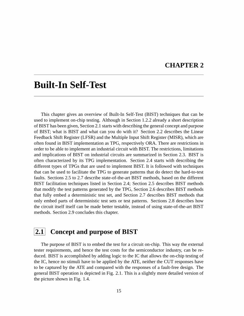
BIST TPGs are often implemented by means of an LFSR[Bar87]. The general struc-ture of an LFSR is depicted in Fig. 2.2. An LFSR is composed of R memory cells (cellsM0 to MR−1 in Fig. 2.2) connected together as a shift register with linear feedbacks (exclu-sive or (exor) function). The variables hr, with 0 ≤ r ≤ R− 1, the feedback coefficients,indicate whether there exists a feedback connection from the output of memory cell MR−1
to the input of memory cell Mr. These coefficients can be 0 (no feedback connection) or 1(feedback connection).
The next state of an LFSR is uniquely determined from the previous state by thefeedback network. Given an initial state, or seed, the LFSR will generate a sequence ofdifferent states, as illustrated by the LFSR given in Fig. 2.3. As soon as a state repeats,
2.2. TPG AND ORA 17
h h
exormemory cell
serial output
hh0
Parallel outputs (PIs)
(scan−chain)M M M M
1 2
0 1 2 R−1
R−1
Figure 2.2: Linear Feedback Shift Register
2 31
0 1 2 3
0011110
1111001
10
11100
1001111
0M M M M
M M M M
Figure 2.3: A 4-bit LFSR
all following states will also repeat; the sequence of states is periodic. Given the seed of0110, the 4-bit LFSR in Fig. 2.3 will generate a sequence of six different states. Whenthe parallel outputs of the LFSR are connected to the PIs of the CUT, this LFSR wouldapply 6 of the 16(=24) possible test patterns to the CUT. LFSRs can also apply PR pat-terns to scan-chains. In that case the last memory cell is often used as serial input for thescan-chain.
An LFSR can be characterized by its characteristic polynomial (ChPol). The ChPolof an R-bit LFSR is given in Eq. 2.1.
ChPol(x) = h0 +h1 · x+h2 · x2 + · · ·+hR−1 · x
R−1 + xR (2.1)
A ChPol is called a primitive ChPol when the corresponding R-bit LFSR would gener-ate a sequence of 2R − 1 different states, given any non-zero seed. This is also called amaximum length sequence and the corresponding LFSR is called a maximum configuredLFSR. Because an LFSR is linear, an LFSR initialized with the all-zero pattern will al-ways generate the all-zero pattern.
The next state of the LFSR can be calculated by multiplying the current state of the

18 CHAPTER 2. BUILT-IN SELF-TEST
0 1 0 . . . 00 0 1 . . . 0. . . . . . . . . . . . . . .0 0 0 . . . 1h0 h1 h2 . . . hR−1
Figure 2.4: The characteristic matrix of an LFSR
h1h0
1
h
2
2
Parallel outputs (primary inputs)
serial output(scan chain) 0M M M M
h
R−1
R−1
Figure 2.5: Out-tapping (type-I) Linear Feedback Shift Register
LFSR with the characteristic matrix, Tc, shown in Fig. 2.4. Given the current state X(t),the next state, X(t +1) can be calculated with Eq. 2.2.
X(t +1) = X(t) ·Tc (2.2)
or given the initial state X(0), the state after t cycles is given by:
X(t) = X(0) ·T tc (2.3)
The ChPol given in Eq. 2.1 can be used to describe both an out-tapping (or type-I)LFSR and an in-tapping (or type-II) LFSR. The LFSR depicted in Fig. 2.2 is an in-tappingLFSR; the XOR taps are within the shift register. The out-tapping LFSR represented bythe same ChPol is depicted in Fig. 2.5. The in-tapping LFSR is more commonly usedthan the out-tapping LFSR, but both configurations are found in existing BIST schemes.
2.2.2 Multiple Input Shift Register (MISR)
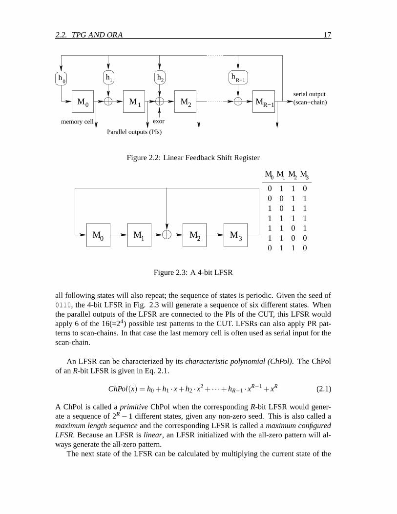
As ORA often the Multiple Input Shift Register (MISR) [Bar87] is used. The MISRis depicted in Fig. 2.6. A MISR is quite similar to an in-tapping LFSR, it consists of R
memory cells (M0 . . .MR−1) with linear feedbacks from cell MR−1. However, the MISR isalso fed by the POs of the CUT. Like the LFSR, the MISR can be characterized by the
2.3. BIST AND REAL-WORLD CIRCUITS 19
h0
1 2
hh h21
Connected to POs of the CUT
R−1
R−1
0M M M M
Figure 2.6: A Multiple Input Shift Register
polynomial given in Eq. 2.1. Given the ChPol and the initial state of the MISR, everycycle the MISR will generate a new state, based on the current state, the ChPol and theresponse of the CUT. The state of the MISR is referred to as the signature. Given theinitial state, the ChPol and the set of responses from the CUT to a given test, the signatureof the MISR after the complete test can be determined. This signature is compared tothe signature of a simulated fault-free circuit. When these signatures do not match, theCUT is not fault-free. However, it is possible that due to aliasing, the signature of theCUT matches the signature of the fault-free circuit, while not all responses were correct.In [Bar87] it is shown that the probability on aliasing can be approximated with Eq. 2.4,where R is the number of stages in the MISR.
p(aliasing) ≈12R (2.4)
Eq. 2.4 shows that the probability on aliasing is independent of the number of test patterns.As long as the number of MISR cells is large enough; e.g., for RMISR ≥ 16, the probabilityof aliasing is almost negligible (≤ 0.0015%).
2.3 BIST and real-world circuits
BIST is not straightforwardly suitable for implementation in every circuit. A circuitmust meet several requirements, especially with respect to high impedance and unknownvalues, before BIST can successfully be applied.
As described in Section 2.2, MISRs are often used as ORA. In order to get a correctand known signature in the MISR, no ’unknown’ or floating values are allowed to beshifted in the MISR during test. When such a value is shifted in the MISR, the completeMISR state becomes unknown and it cannot be checked whether the signature conformsto a fault-free circuit. Therefore a circuit should satisfy the following requirements forsuccessful BIST implementation:
1. There are no floating/unknown circuit inputs that can propagate to the MISR.

20 CHAPTER 2. BUILT-IN SELF-TEST
2. POs that can float or be unknown should not be connected directly to the MISR inorder to avoid an unknown MISR signature.
These requirements can be satisfied when:
• Embedded memory inputs, bi-directional inputs and other possibly floating inputsor inputs with an unknown value are set to a known value by extra test-logic.
• Bus-drivers of three-state buses are never enabled at the same time, regardless ofthe circuit’s input values,in order to avoid bus-conflicts and hence buses becomingunknown.
• POs that can float, e.g., due to floating buses, should be pulled-up or pulled-downbefore their value is shifted into the MISR.
• POs that cannot be pulled-up/pulled-down and still can float or can become un-known should not be connected to the MISR. This has a negative impact on theachievable fault coverage, because an unknown MISR signature means no faultcoverage at all.
Bus-conflicts should be avoided regardless whether they can result in unknown MISRsignatures because they can cause circuit damage. ATPGs do avoid bus-conflicts by notgenerating test patterns that cause bus-conflicts, but PRTPGs do not! Because PRTPGsare often used in BIST implementations, one should make sure that buses in the circuitcan never become conflicting regardless of the circuit input values.
In Gu et al. [Gu 01] techniques are described, to overcome BIST problems e.g., timingviolations and unknown MISR signatures due to unknowns, that can be used to minimizethe designs efforts with respect to BIST implementation in industrial designs.
In general, BIST implementations assume that the circuit confirms to a full-scan de-sign. In order to be able to reach high enough fault coverages, all memory elements (i.e.,flipflops, latches) should be made scannable such that their values can be controlled andobserved.
2.4 BIST implementations
In order for BIST to be successful, BIST implementations have to meet the followingrequirements:
1. Low hardware overhead
2. Low test application time (i.e., low number of applied test patterns)
3. High enough fault coverage in order to meet the test quality requirements

2.4. BIST IMPLEMENTATIONS 21
Especially the first two points are hard to achieve at the same time. Several state-of-the-artBIST methods mainly focus on low hardware overhead [Lis87, Wai89, Hel92, Lem94],while other methods focus mainly on low test application times [Nag95, Duf91, Duf93,Vas93]. One of the main differences in all BIST implementations found in literature is thetype of TPG that is used. Basically, TPGs can be divided into the following three groups:
1. Exhaustive TPG (XTPG)
2. Pseudo random TPG (PRTPG)
3. Deterministic TPG (DTPG)
Each of these groups of TPGs have their own advantages/disadvantages with respect tohardware overhead, test application time and fault coverage. This will be described inSubsections 2.4.1 to 2.4.3.
2.4.1 Exhaustive test pattern generator (XTPG)
The (theoretical) XTPG generates all possible test patterns. If a circuit has n PIs, theXTPG will generate 2n patterns1. The XTPG generates all possible patterns and hencewill also detect all possible detectable single SAFs; the fault coverage will be high. How-ever, one can imagine that this large number of test patterns that have to be generated willnot be feasible for large designs. Consider ISCAS’85 circuit c7552, see Appendix A. Thiscircuit has 207 inputs (both PI and SFF inputs). An XTPG would have to generate 2207
patterns! Therefore, the XTPG is not practical for nowadays complex industrial designsas they often have far more than 207 inputs. In general one can say that the XTPG has a
+ low hardware overhead
– very large test application time
+ complete fault coverage (all detectable faults are covered)
The large number of test patterns of the XTPG can be reduced considerably whena pseudo exhaustive test pattern generator (PXTPG) is used. In this case the circuit isfirst partitioned into several independent sub-circuits. Each sub-circuit is tested with anXTPG. Because the number of PIs for each sub-circuit is much lower than the total num-ber of PIs, the total number of test patterns that have to be generated can be reducedconsiderably.
Fig. 2.7(a) shows an example circuit with 16 PIs. The 16-bit XTPG will generate 216
= 65536 patterns. Fig. 2.7(b) shows the same circuit in case PXTPG-testing is used. Thecircuit of Fig. 2.7(a) has been divided into three independent sub-circuits with respec-tively 4, 7, and 5 PIs. Each of these sub-circuits can be tested with an XTPG. Because the
1Or 2n −1 patterns, because often the all-zero pattern will not be applied

22 CHAPTER 2. BUILT-IN SELF-TEST
16−
bit X
TPG
CircuitUnderTest
(a) XTPG
7−bi
t XT
PG
Sub−circuit 1
Sub−circuit 3
Sub−circuit 2
(b) PXTPG
Figure 2.7: (Pseudo) exhaustive test pattern generators
sub-circuits are independent, they can be tested in parallel by using the same XTPG withas width the number of inputs of the sub-circuit with the largest number of PIs. In theexample, this sub-circuit has 7 inputs and hence 27 = 128 test patterns will be generated,significantly less than the initial 65536 test patterns.
Although the number of test patterns that will be generated by a PXTPG is alreadyreduced enormously, the PXTPG is still not very practical. Partitioning the circuit intoindependent sub-circuits is a complex problem by itself (NP complete) and is not alwayspossible. Even when such sub-circuits are found, they are often still too large to be testedby a XTPG.
2.4.2 Pseudo random test pattern generator (PRTPG)
A PRTPG generates a set of PR test patterns which are applied to the CUT. These pat-terns are generated without taking into account any knowledge about the CUT structure.The patterns generated by a PRTPG are not really random, because they are determineddeterministically by the implementation of the TPG. Although the patterns seem to berandom, the PRTPG will generate the same sequence of patterns given the same initialpattern. Therefore this TPG is called a pseudo random test pattern generator.
Usually only a small subset of all possible test patterns are generated by the PRTPG.This way the test application time can be kept low, however at the cost of a lower faultcoverage. Because the patterns are generated without any knowledge of the CUT, it cannot always be guaranteed that all stuck-at faults are covered.
PRTPGs are often implemented by means of an LFSR or Cellular Automaton (CA)[Hor89]. Although an LFSR has very low hardware overhead, the patterns generated bythe LFSR often fail to detect faults known to be Random Pattern Resistant (RPR). RPR

2.4. BIST IMPLEMENTATIONS 23
80
85
90
94
96
98
99
100
64 256 1024 4096 16384 65536 262144 1.04858e+06Number of applied PR test patterns
fault coverage
Fault efficiency as function of the number of applied PR test patterns for circuit c7552.Fa
ult e
ffic
ienc
y (%
)
Figure 2.8: Fault efficiency versus number of applied PR patterns plot
faults are faults which can only be detected by a very small set of test patterns. Mostfaults, i.e., non RPR faults, can be detected by a relative large set of different test patterns.Because it is not feasible (with respect to test application time) to generate all test patterns,the number of test patterns generated by the PRTPG is often only a very small subset ofall possible test patterns. Still it is likely that this subset contains at least one pattern withwhich a non RPR fault can be detected. Because there are only very few patterns whichwill detect an RPR fault, it is unlikely that this subset contains a pattern with which anRPR fault will be detected. Hence, the RPR faults remain undetected, reducing the faultcoverage. Again one could increase the number of generated test patterns, but this willresult in unacceptable long test application times.
Fig. 2.8 shows a plot of a PRTPG run on ISCAS’85 circuit c7552. The figure showsthe fault efficiency as function of the number of applied PR test patterns. Note that thex-axis is in log2-scale! In Chapter 1, the fault coverage has been defined as the ratio ofthe number of actual detected faults and the total number of faults in the IC; the faultefficiency, on the other hand, is defined as the ratio of the number of actual detected faultsand the number of detectable faults in the IC, i.e., the fault efficiency does not take intoaccount faults that cannot be detected.
Fig. 2.8 shows that less than 200 PR patterns are required to reach 90% fault effi-ciency. Also 94% fault efficiency has been reached with less than 2000 PR test patterns.
24 CHAPTER 2. BUILT-IN SELF-TEST
But increasing the fault efficiency from 94% to 96% becomes already harder, althoughthe number of required patterns is still acceptable in most cases; after 15,000 patterns the96% level has been reached. But the remaining 4% becomes a problem. The 98% faultefficiency level already requires 180,000 patterns, more than 10 times as much as the 96%level. And even after applying 1 million PR test patterns, the 99% fault efficiency levelhas not been reached. This means that even for such a small circuit as the c7552 (only3512 gates), over 1% of all detectable faults cannot be detected after applying one millionPR patterns. In general one can say that the PRTPG has a
+ low hardware overhead
- large test application time
- low fault coverage
2.4.3 Deterministic test pattern generator (DTPG)
Both the XTPG and the PRTPG generate a lot of test patterns which are useless, thesetest patterns do not detect any ’new’ faults that were not already detected by other patterns.A deterministic TPG generates a set of deterministic test patterns, often generated by anATPG tool. These deterministic test patterns do contribute to detecting ’new’ faults. Bygenerating deterministic patterns, often the number of test patterns that have to be appliedis low (short test application times), while still high fault coverages can be reached. Thedeterministic test patterns will contain the patterns that detect RPR faults.
However, the deterministic test patterns have to be stored in some way in the TPG. Thestate-of-the art deterministic BIST methods [Nag95, Duf91, Duf93] handle this in variousways as described in the following section. One of the most simple implementationswould be using an embedded Read-Only Memory (ROM). But for a circuit with manyPIs and/or test patterns, the size of the ROM and hence the hardware overhead becomesunpractical large. For example, ISCAS’85 circuit c7552 with 207 inputs requires 128ATPG test patterns (see Appendix A) for 100% fault efficiency. Hence a 26496 bits ROMwould be required for a circuit with only 3512 gates, this would be an enormous overhead.In general one can say that a DTPG has a
– high hardware overhead
+ low test application time
+ high achievable fault coverage
2.4.4 BIST facilitation techniques
Fig. 2.9 shows a schematic test time versus hardware plot for several BIST methods.The ROM acting as DTPG and the LFSR acting as XTPG are put in this plot as extremes.
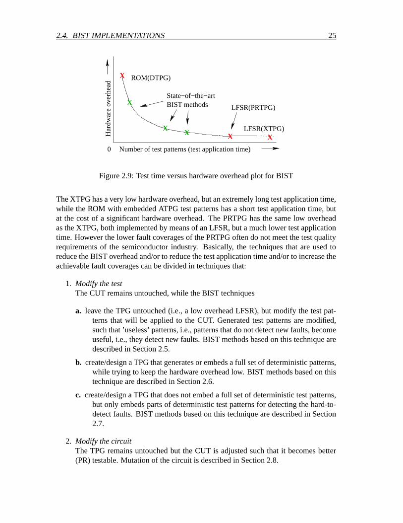
2.4. BIST IMPLEMENTATIONS 25
0
State−of−the−artBIST methods
ROM(DTPG)
X
LFSR(PRTPG)
LFSR(XTPG)
X
XXH
ardw
are
over
head
Number of test patterns (test application time)
X
X
Figure 2.9: Test time versus hardware overhead plot for BIST
The XTPG has a very low hardware overhead, but an extremely long test application time,while the ROM with embedded ATPG test patterns has a short test application time, butat the cost of a significant hardware overhead. The PRTPG has the same low overheadas the XTPG, both implemented by means of an LFSR, but a much lower test applicationtime. However the lower fault coverages of the PRTPG often do not meet the test qualityrequirements of the semiconductor industry. Basically, the techniques that are used toreduce the BIST overhead and/or to reduce the test application time and/or to increase theachievable fault coverages can be divided in techniques that:
1. Modify the testThe CUT remains untouched, while the BIST techniques
a. leave the TPG untouched (i.e., a low overhead LFSR), but modify the test pat-terns that will be applied to the CUT. Generated test patterns are modified,such that ’useless’ patterns, i.e., patterns that do not detect new faults, becomeuseful, i.e., they detect new faults. BIST methods based on this technique aredescribed in Section 2.5.
b. create/design a TPG that generates or embeds a full set of deterministic patterns,while trying to keep the hardware overhead low. BIST methods based on thistechnique are described in Section 2.6.
c. create/design a TPG that does not embed a full set of deterministic test patterns,but only embeds parts of deterministic test patterns for detecting the hard-to-detect faults. BIST methods based on this technique are described in Section2.7.
2. Modify the circuitThe TPG remains untouched but the CUT is adjusted such that it becomes better(PR) testable. Mutation of the circuit is described in Section 2.8.

26 CHAPTER 2. BUILT-IN SELF-TEST
2.5 BIST facilitation techniques: Modify the test pat-terns
This section describes three BIST techniques, which modify the test patterns gen-erated by a PRTPG in such a way that the fault-coverage will be increased. They aredescribed in Subsections 2.5.1-2.5.3.
2.5.1 Reseeding of the LFSR
The LFSR starts generating patterns, given the seed of the LFSR. An R-bit LFSRwith a primitive ChPol will generate all possible R-bit patterns, hence also the patternsthat detect RPR faults. However, it might take a while before the LFSR generates a testpattern for a specific RPR fault. But with a right chosen seed, several RPR faults can bedetected with only a few patterns, e.g., using a test pattern as seed that detects very hardRPR faults.
[Lem94] describes a method based on discrete logarithms [Poh78], which selects theChPol and the seed of the LFSR which results in the smallest test sequence, detecting agiven set of RPR faults. However, for circuits with many RPR faults, still a very large testsequence is necessary to cover most, if not all, RPR faults.
Instead of using one seed, reseeding can be used to make sure that most of the RPRfaults are covered by the test sequence. After a first set of test patterns is generated usingan initial seed, the LFSR is re-initialized with a new seed. This way a sequence of uselesstest patterns can be skipped, such that the LFSR will continue generating test patterns thatdo detect (RPR) faults.
[Hel92] describes a method which uses a partially reconfigurable LFSR and reseeding
Dec
odin
gL
ogic
ORA(SR)Scan−chain
CUT
Poly. Id Seeds
&&&
Multiple−polynomial LFSR
Figure 2.10: BIST scheme using Multiple-polynomial LFSR with reseeding

2.5. BIST FACILITATION TECHNIQUES: MODIFY THE TEST PATTERNS 27
0.5 / 0.50.5 / 0.50.5 / 0.50.5 / 0.50.5 / 0.50.5 / 0.50.5 / 0.50.5 / 0.50.5 / 0.50.5 / 0.5
0.999 / 0.001
0 / 1 Probability
&
(a) Uniform 0/1 distribution
0.1 / 0.90.1 / 0.90.1 / 0.90.1 / 0.90.1 / 0.90.1 / 0.90.1 / 0.90.1 / 0.90.1 / 0.90.1 / 0.9
0.651 / 0.349
0 / 1 Probability
&
(b) Non-uniform 0/1 distribution
Figure 2.11: Impact input-value distribution on testability of a CUT
techniques to reduce the number of test patterns while keeping a high fault coverage.Partial reconfigurable means that the LFSR embeds multiple primitive ChPols and theLFSR can operate according to one of these ChPols. This BIST scheme is depicted in Fig.2.10. Given the used ChPol (by the Polynomial Identifier (Poly. Id)) and the correspondingseed, the Decoding Logic enables/disables feedback loops through the AND-gates. TheChPol and seeds are chosen in such a way that test patterns for hard-to-detect faults willbe generated. The PR bits generated by the out-tapping LFSR are shifted into the scan-chain of the CUT. The response of the CUT will be shifted out through the scan-chaininto the ORA, implemented as a Signature Register [Bar87]. [Hel92] shows that thisBIST scheme reduces the linear dependences between the bits shifted in the scan-chain.However, it is also mentioned that applications of this scheme are seen in the area ofPXTPG, which means that the test application times still tend to be large for nowadayslarge and complex circuit designs.
2.5.2 Weighted Random TPG
When an LFSR is used as TPG, especially in case the LFSR has a primitive ChPol, thePI values will be uniformly distributed, i.e., each input will have a probability of 0.5 to beassigned a 0 or a 1. However, there are faults in the circuits which require a non-uniformdistribution of 0 and 1 on the PIs in order to have a reasonable high probability to becomedetected by a PR pattern. This is illustrated in Fig. 2.11.
If all inputs of the 10-input AND-gate in Fig. 2.11(a) have an equal probability to beassigned 0 or 1, the probability that a SA0 fault at the output of the AND-gate will be

28 CHAPTER 2. BUILT-IN SELF-TEST
&0.5 / 0.50.5 / 0.5
0.5 / 0.5
>1
1−0.5 /N
0.5
0.5 / 1−0.5N N
X
X
1X2X
N
N
2X1X
N
(a) Uniform 0/1 distribution
&
XX
X
>1
N N
N N
0.1 / 0.90.1 / 0.9
0.1 / 0.9
1−0.9 / 0.9
0.1 / 1−0.1
N
2
1
X N
2X1X
(b) Non-uniform 0/1 distribution
Figure 2.12: Changing input-value distribution has positive impact on several faults andnegative impact on other faults
detected2 is very low (0.510). However, when these inputs have a much higher probabilityon a 1 than on a 0, the probability that the SA0 fault at the output will be detected, is muchhigher, as illustrated in Fig. 2.11(b).
Such a set of input values with a non-uniform distribution is called a weight set. Sev-eral faults which are RPR in case of a uniform input distribution, become much moretestable with a certain weight set. However, this weight set can make one set of RPRfaults better testable, but another group of faults worse testable. This is illustrated in Fig.2.12. By increasing the probability of a 1 on the inputs of the gates, the probability that theSA0 fault at the output of the AND-gate will be detected, increases significantly, howeverat the same time, the probability of detecting the SA1 fault at the output of the OR-gate isreduced.
In order to be able to improve the detectability of all RPR faults in the CUT, multipleweight sets are required. In this case, the applied test set will be divided into sub test-sets.The first group of test patterns will be applied using weight set 1, the following group oftest patterns will be applied using weight set 2, etc.. To apply weighted input values to theCUT, Boolean logic is required which converts uniformly distributed LFSR outputs intoweighted inputs values for the CUT. E.g., in order to get a weight of 0.25 on a 1, a 2-inputAND-gate can be used. The inputs of the AND-gate are connected to the LFSR and willhave a probability of 0.5 on a 1. The output of the AND-gate will have a probability of0.75 on a 0 and a probability of 0.25 on a 1.
The weighted random methods differ in the way they determine the weights. Severalmethods use testability analysis measures and heuristics to determine the weights [Lis87,Wai89], other methods use the input-value distribution of deterministic, i.e., ATPG, gen-erated test sets [Mur90, Pom93], and again other methods are a combination of testability
2a SA0 fault at a line can only be detected, when that line is 1 in the fault-free case

2.5. BIST FACILITATION TECHNIQUES: MODIFY THE TEST PATTERNS 29
Table 2.1: Weighted random benchmark results of several ISCAS’85 circuits
Circuit #Wt. sets #WR pat. Circuit #Wt. sets #WR pat.c880 2 1280 c3540 4 3840c1355 3 2098 c5315 2 2048c1908 6 5376 c6288 1 512c2670 8 5888 c7552 10 9278
analysis and deterministic test distribution [Ree96].Table 2.1, taken from [Wai89], shows weighted random benchmark results. Column
Circuit shows the circuit name, Column #Wt. sets the number of weight sets that werenecessary to detect all faults in the circuit, and column #WR pat. the number of weightedrandom patterns necessary to test all faults. [Wai89] only uses weights 1/16, 1/2 and 15/16for input values. As could be expected, these results show that circuits which are knownto be RPR, e.g., circuits c2670 and c7552, require more weight sets than more randomsusceptible circuits like the c880, c1355, c5315 and c6288. The number of weight setsfor circuit c2670 and c7552 is quite large to be implemented for such small circuits (only1193, respectively 3512 gates).
Also other weighted random results have shown that often a large number of differentweight sets are required in order to achieve a high enough fault coverage within a reason-able test length. The logic overhead, necessary to enable the different weight sets, can bequite large. This overhead can be reduced by decreasing the number of weight sets and bylimiting the number of allowed weights.3. However, this will decrease the fault coverageand increase the test length.
2.5.3 Mapping logic to replace useless patterns
LFSRs/CAs used as PRTPG generate lots of test patterns that do not detect faultswhich were not already detected by previous test patterns. Mapping logic is logic whichconverts these ’useless’ patterns into patterns which do detect faults that were not detectedpreviously. Converting useless test patterns into patterns that detect RPR faults would beespecially interesting. [Tou95] introduces such a method, which is based on cube map-ping.
Test cube: A w-bit test cube Cu is a test pattern for which not all w bits necessarily havea specified value, i.e., Cu = (c1,c2, . . . ,cw) ∈ {0,1,x}w with x representing don’t care.
A test pattern A = (a1,a2, . . . ,aw) ∈ {0,1}w is contained in a test cubeCu = (c0,c1, . . . ,cw) ∈ {0,1,x}w if ∀ j,1 ≤ j ≤ w|(a j = c j or c j = x).
3A weight of 0.231 is much more expensive in logic than a weight of 0.25 (2-input AND-gate)

30 CHAPTER 2. BUILT-IN SELF-TEST
1a
a2
a3
1b
b2
b3
Mapping Logic
Out
put t
o C
UT
Inpu
t fro
m P
RT
PG
&
1
&
testmode
(a) Cube mapping logic
1a a2 a3 1b b2 b3
00001111
00000011
01110101
00001111
00110011
01010101
(b) Mapped patterns
Figure 2.13: Cube mapping with source cube sCu={0 1 X} and image cube iCu={X 0 1}
The Cube Mapping CM : {0,1}w → {0,1}w is defined as follows: Given the sourcecube sCu = (s0,s1, . . . ,sw) and image cube iCu = (i0, i1, . . . , iw), then the Cube MappingCMsCu→iCu(A) = B = (b0,b1, . . . ,bw) ∈ {0,1}w where if test pattern A is contained insCu, then if i j = x then b j = a j else b j = i j. If test pattern A is not contained in sCu, thenb j = a j∀ j. In other words, when pattern A is contained in sCu, pattern A is transformedinto a pattern which is contained in iCu. When A is not contained in sCu, A stays the same.
Given a required fault coverage level and given a maximum test length, the method de-scribed in [Tou95] tries to determine the mapping logic (based on cube mapping) requiredto reach this fault coverage level. The steps applied during this method are:
1. Do fault simulation on the set of test patterns generated by the PRTPG (LFSR).
2. Evaluate the fault coverage and identify the set of undetected faults
3. If the fault coverage is high enough, the process is finished.
4. If not, add a cube mapping.
5. Compute the transformed pattern set and do fault simulation on this test pattern setand go to step 2.
Fig. 2.13(a) shows an example of mapping logic based on cube mapping. In normalapplication mode (test mode = 0), the values on b{1,2,3} that will feed the CUT will bethe same as on a{1,2,3} applied by the PRTPG. In test mode (test mode = 1), the valuesa applied by the PRTPG are mapped according to the cube mapping CM{01X}→{X01}.The corresponding mapping logic is shown in Fig. 2.13(a) and the corresponding patternmapping is shown in Fig. 2.13(b).
The key problem that this method tries to solve is how to find the right cube mappings.

2.5. BIST FACILITATION TECHNIQUES: MODIFY THE TEST PATTERNS 31
The described method in [Tou95] is based on solving a binate covering problem [Bra89].Although good heuristics exist, the CPU requirements for solving the NP-complete binatecovering problem still make this method infeasible for large industrial circuits.
2.5.4 Comparison of test pattern mutation techniques
Table 2.2 shows experimental results of weighted random testing and cube mapping.The table also contains experimental results of the fixed-biased BIST method [Als94],which is described further on in Subsection 2.7.2. Results are shown for several ISCASbenchmark circuits [Brg85, Brg89] and are taken from [Tou95].
Column Circuit in Table 2.2 shows the circuit name. Columns Gates and FFs show thenumber of gates, respectively the the number of FFs in the circuit; while Column Random
length shows the number of required PR test patterns in order to reach 100% fault cover-age of all detectable faults, when only an LFSR is used to generate the patterns. Columns3-Weight, Fixed-biased and Cube mapping show the results for respectively the weightedrandom method proposed by Pomeranz and Reddy [Pom93], the fix-biased method pro-posed by Alshaibi and Kime [Als94], and the cube mapping method proposed by Toubaand McCluskey[Tou95]. For each of these methods, the hardware overhead is shown thatcorresponds to reaching 100% fault coverage for the given test length Len. This hardwareoverhead is split into added FFs (Column FFs) and Gate Equivalents (Column GEs), usingthe method suggested in [Har93]: 4 0.5n GEs for an n-input NAND/NOR, 2.5(n−1) GEsfor an n-input XOR, and 1.5 GEs for a 2-to-1 multiplexer.
These results show that the extra hardware overhead inserted to reduce the test lengthcan be enormous and be more than the size of the circuit itself. Using the weightedrandom method of Pomeranz, the overhead can be over 100% as for circuit c2670, the
4One GE equals the size of a two-input NAND gate
Table 2.2: Comparison of Test Length and Required Hardware
Random 3-Weight Fixed-biased Cube mappingCircuit Gates FFs length Len FFs GEs Len FFs GEs Len FFs GEs
s420 196 16 1.1M N/A N/A N/A 5K 18 >7 500 0 481K 0 31
s641 379 19 1.0M N/A N/A N/A 19K 20 > 21 500 0 2310K 0 12
s838 390 32 >100M N/A N/A N/A 86K 19 >14 850 0 9910K 0 59
c2670 1193 0 4.6M 19K 5 1507 19K 54 >259 1K 0 26030K 5 1316 7K 0 114
c7552 3512 0 >100M 47K 6 3003 191K 111 >658 10K 0 21472K 6 2475 50K 0 183

32 CHAPTER 2. BUILT-IN SELF-TEST
overhead in GEs is 1316 or 1507 GE, depending on the test length, which are both morethan the 1193 gates the circuit itself consists of. In case cube mapping is used, the hard-ware overhead is much less, but still often over 5%, which is already considered too muchby most manufacturers. 114 GEs for circuit c2670 is still 9.5% overhead.
2.6 BIST facilitation techniques: Fully embedded deter-ministic test patterns
The following methods modify the TPG/LFSR in such a way that the TPG/LFSR alsogenerates a full set of deterministic test patterns. The deterministic test set (e.g., generatedby an ATPG) contains also patterns for the RPR faults such that the fault coverages achiev-able with BIST can be improved. Subsections 2.6.1, 2.6.2 and 2.6.3 describe respectivelythe pre-stored test BIST method, the LFSROM BIST architecture and the deterministicLFSR.
2.6.1 The pre-stored test BIST method
The pre-stored test BIST method [Nag95] uses the response of the CUT to generatethe next test pattern. The TPG is implemented as a Finite-State-Machine (FSM). The TPGruns through a sequence of states and each state represents a test pattern. The next state(hence, next test pattern) depends on the response of the CUT. If the CUT has a correctresponse, the TPG will come in the next valid state and will apply the pattern to the CUT,else the TPG will come in a different state and hence will apply a different pattern to the
S0
0001
S1
0011
S2
0110
F5
S3S4
S9S8
S5
S6
S7
100010011010
1100
1011
0101 1110
1111
F1
0000 F2
0100 F30111
F4
1101
0010
F6
Faulty−free response
Faulty response A State
Figure 2.14: The state-sequence of the Pre-stored Test BIST method

2.6. BIST FACILITATION TECHNIQUES: FULLY EMBEDDED DETERMINISTICTEST PATTERNS 33
Table 2.3: Hardware overhead and Fault coverage of a Pre-stored BIST
Test Fault HardwareCircuit Gates patterns coverage overhead74283 35 11 100% 15%74181 61 17 100% 7%74280 55 11 100% 4%74885 87 48 100% 27%c432 160 34 99% 11%c499 202 43 100% 18%c880 383 51 99% 9%c1355 546 85 100% 10%c1908 880 119 100% 9%
CUT. A graphical representation of an example FSM is depicted in Fig. 2.14.If all responses are correct and given that the FSM will start in state S0, the FSM will
run through the sequence of states S0, S1, . . ., S9 to S0. If an error occurs somewhere inthis sequence, the TPG will follow another sequence of states and will return in a differentend state after 9 applied test patterns. The states F1. . .F6 can only be reached when anerror occurred during the test and are considered fault states. So, without errors, the FSMwill end in the state in which it started and one only has to check if this end state equalsthe initial state. Nagvajara [Nag95] describes how the FSM should be designed such thatit has a low probability of aliasing. In this case aliasing is the effect that a faulty circuitends in state S0, because then it would falsely be considered a fault-free circuit.
Table 2.3 shows experimental results for the pre-stored test, taken from [Nag95]. Onlyresults for some very small circuits are shown. Columns Circuit and Gates show the nameof the circuit respectively the number of gates in the circuit. Column Test Patterns showsthe number of ATPG test patterns needed to reach the fault coverage shown in ColumnFault Coverage. Column Hardware overhead shows the hardware overhead (percentage) ofthe FSM.
The hardware overhead of this BIST system is linear with the number of pre-storedtest patterns and the pattern size. Therefore, this method is only feasible for circuits witha very compact ATPG test set which can be pre-stored. Otherwise, although often 100%fault coverage is achieved, the hardware overhead will be far over 5% and will be oftenconsidered too high by IC manufacturers. In Table 2.3 only circuit 74280 results in lessthan 5% overhead, all other circuits result in more overhead; up to 27% for circuit 74885.

34 CHAPTER 2. BUILT-IN SELF-TEST
2OR Gates Network
Ac0 1 AcB−1
b−to−1 Multiplexerw−bit wide
t0
t1
tb−1 w
w
wwt
Ac
R−bit Shift Register Asynchronous Counter
CUTM
0M
1M
2 MR−1
LFSROM
Figure 2.15: The LFSROM architecture
2.6.2 The LFSROM architecture
The LFSROM architecture, presented in [Duf93], uses a shift register in combina-tion with an OR2 gates (2-input OR gates) network to store a deterministic test set; theLFSROM stores a deterministic test set containing T test patterns of w bits width. It iscomposed of the following four parts, depicted in Fig. 2.15:
1. A R-bit shift register
The R-bit shift-register shifts through the states from [100· · ·0], [010· · ·0] to [000· · ·1]with a cyclic period R.
2. An OR2 gates network
The R states of the shift register are transformed into R deterministic test patternsby the OR2 gates network. These test patterns are w bits wide.
3. A w-bit wide b-to-1 multiplexer
Instead of generating R test patterns, the test set contains T deterministic test pat-terns that have to be generated. Multiple subsets of test patterns can be generatedby the OR2 gates network in parallel. The w-bit wide multiplexer can be used toselect one of the b = dT/Re subsets of test patterns.
4. An Asynchronous Counter
An B = dlog2(b)e bit asynchronous counter is used control the multiplexer and toselect which of the b subsets of test patterns will be applied to the CUT.
Table 2.4 shows experimental results for the LFSROM architecture, taken from [Duf93].The overhead of the LFSROM architecture is compared to the overhead of using a ROMto store the test patterns. Column Circuit shows the circuit name, Columns T and w showrespectively the number of test patterns to store and the width of the test patterns. Col-umn R shows the length of the R-bit shift register and Column b shows the value for b ofthe b-to-1 multiplexer. Columns ROM mm2 and LFSROM mm2 show the silicon-size of the
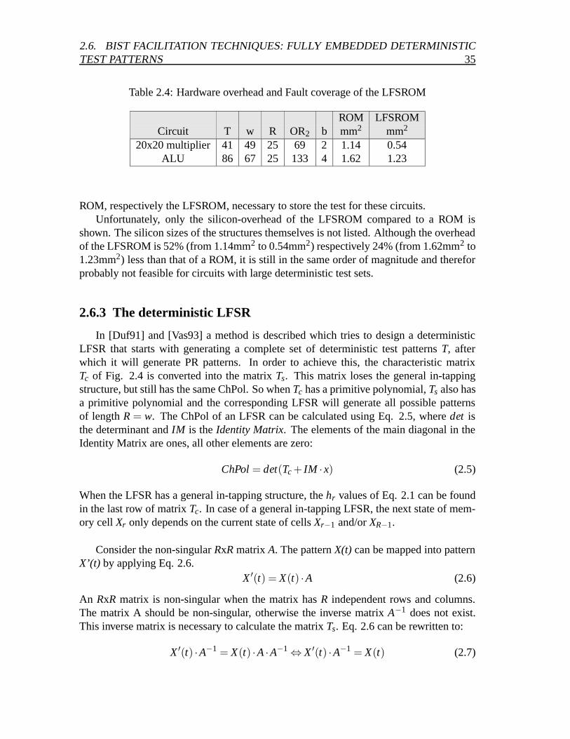
2.6. BIST FACILITATION TECHNIQUES: FULLY EMBEDDED DETERMINISTICTEST PATTERNS 35
Table 2.4: Hardware overhead and Fault coverage of the LFSROM
ROM LFSROMCircuit T w R OR2 b mm2 mm2
20x20 multiplier 41 49 25 69 2 1.14 0.54ALU 86 67 25 133 4 1.62 1.23
ROM, respectively the LFSROM, necessary to store the test for these circuits.Unfortunately, only the silicon-overhead of the LFSROM compared to a ROM is
shown. The silicon sizes of the structures themselves is not listed. Although the overheadof the LFSROM is 52% (from 1.14mm2 to 0.54mm2) respectively 24% (from 1.62mm2 to1.23mm2) less than that of a ROM, it is still in the same order of magnitude and thereforprobably not feasible for circuits with large deterministic test sets.
2.6.3 The deterministic LFSR
In [Duf91] and [Vas93] a method is described which tries to design a deterministicLFSR that starts with generating a complete set of deterministic test patterns T, afterwhich it will generate PR patterns. In order to achieve this, the characteristic matrixTc of Fig. 2.4 is converted into the matrix Ts. This matrix loses the general in-tappingstructure, but still has the same ChPol. So when Tc has a primitive polynomial, Ts also hasa primitive polynomial and the corresponding LFSR will generate all possible patternsof length R = w. The ChPol of an LFSR can be calculated using Eq. 2.5, where det isthe determinant and IM is the Identity Matrix. The elements of the main diagonal in theIdentity Matrix are ones, all other elements are zero:
ChPol = det(Tc + IM · x) (2.5)
When the LFSR has a general in-tapping structure, the hr values of Eq. 2.1 can be foundin the last row of matrix Tc. In case of a general in-tapping LFSR, the next state of mem-ory cell Xr only depends on the current state of cells Xr−1 and/or XR−1.
Consider the non-singular RxR matrix A. The pattern X(t) can be mapped into patternX’(t) by applying Eq. 2.6.
X ′(t) = X(t) ·A (2.6)
An RxR matrix is non-singular when the matrix has R independent rows and columns.The matrix A should be non-singular, otherwise the inverse matrix A−1 does not exist.This inverse matrix is necessary to calculate the matrix Ts. Eq. 2.6 can be rewritten to:
X ′(t) ·A−1 = X(t) ·A ·A−1 ⇔ X ′(t) ·A−1 = X(t) (2.7)
36 CHAPTER 2. BUILT-IN SELF-TEST
Combining Eqs. 2.2 and 2.7, we get:
X ′(t +1) ·A−1 = X ′(t) ·A−1 ·Tc
X ′(t +1) = X ′(t) ·A−1 ·Tc ·A
and finally into:X ′(t +1) = X ′(t) · (A−1 ·Tc ·A) = X ′(t) ·Ts (2.8)
Ts and Tc are called similar matrices; these matrices possess the same ChPol [Duf91]:det(Tc + I · x) = det(Ts + I · x).
The LFSR corresponding to the matrix Ts can be found as follows: The next stateof memory cell Xi can be found by taking the exclusive OR of the current states of thememory cells X j for which element ( j, i) (row j and column i) in matrix Ts is 1.
According to [Poh78], when the Tc is initialized with the state X(0)=[100· · ·0], inde-pendent of the ChPol, the LFSR will first generate the following state sequence:
X(t = 0) = [100 · · ·0]
X(t = 1) = [010 · · ·0]
X(t = 2) = [001 · · ·0]... =
...
X(t = N −1) = [000 · · ·1]
When each of these states X(t) is transformed into X ′(t), using Eq. 2.6, it is clear thateach state X ′(t = i) equals to row i of matrix A. Hence, if the LFSR with characteristicmatrix Ts is initialized with the first row of A, all following rows of A will be generated.After all rows of A have been generated, the LFSR continues with the PR states.
So if A would be the test set containing T = R independent deterministic patterns, thismethod can be used to design an LFSR which will generate all test patterns of this testset. However, a drawback of this method is that the LFSR must have the same width (R)as the test patterns (w). For a circuit with many inputs (PIs and SFF outputs), this can beenormous. If the test set A is singular, extra bits or patterns have to be added to make itnon-singular; this will make the LFSR even larger!
Fig. 2.16 shows an example of the deterministic LFSR for a deterministic test setcontaining 4 patterns. Given the seed 0101, which is the first test pattern in test set A, thedeterministic LFSR first generates the remaining patterns/states of test set A, after whichit will generate two PR states before it will generate state 0101 again. The ChPol found inthe last row of the Tc given in Fig. 2.16 is not primitive. Ts has the same non-primitive Ch-Pol and therefore the deterministic LFSR will not generate all 2n−1 = 15 possible states,but only 6 (4 deterministic, 2 PR) different states, given seed 0101.
[Duf91, Vas93] do not show results with respect to the hardware overhead. It is as-sumed that all inputs are controlled through (S)FFs and therefore the LFSR memory cellswill not result in much hardware overhead. However, the main hardware overhead con-sists of the overhead of the necessary XOR gates. In [Geu97a], experimental results for

2.6. BIST FACILITATION TECHNIQUES: FULLY EMBEDDED DETERMINISTICTEST PATTERNS 37
0 1 0 11 0 1 11 1 0 00 0 1 1
Test set A:
Deterministic LFSR corresponding to T
ResultingGiven Given
Sequence generated by LFSR, given initial seed 0101:
MM M M2 310
0101 1011 1100 0011 1001 1000 0101
0 1 0 00 0 1 00 0 0 11 0 1 0
T T
0 1 0 10 1 1 00 1 0 01 1 0 1
sc
s
Figure 2.16: Deterministic test set embedded in an LFSR
the ISCAS’85 benchmark circuits [Brg85] are given of the deterministic LFSR, with re-spect to the number of necessary two-input XOR gates; see Table 2.5.
Column Circuit shows the circuit name, Column #Patterns shows the number of deter-ministic test patterns and Columns #Inputs and #Gates show respectively the number of
Table 2.5: Hardware overhead of the Deterministic LFSR
Circuit #Patterns #Inputs #Gates XOR2
c17 6 5 6 5c245 19 14 63 42c432 45 36 160 306c499 60 41 202 262c880 27 60 383 313c1355 96 41 546 546c1908 127 33 880 766c2670 76 233 1193 2916c3540 130 50 1669 1226c5315 129 178 2307 3708c6288 33 32 2416 201c7552 160 207 3512 5405

38 CHAPTER 2. BUILT-IN SELF-TEST
inputs and the number of gates of the circuit. Column XOR2 lists the number of two-inputXOR gates which are necessary to implement a deterministic LFSR which starts withgenerating all patterns of the deterministic test set. If necessary, extra patterns and or bitsare added in order to get a non-singular NxN test set.
The experimental results in Table 2.5 show that the hardware overhead with respect tothe number of XOR gates, compared to the number of gates in the circuit, is large; circuitsc432, c399, c2670, c5315, 7552 require even more XOR gates than the original numberof gates in the circuit. The remaining circuits, except circuit c6288, require approximatelythe same number of XOR gates compared to the number of gates in the circuit itself. Thismeans that the deterministic LFSR-overhead for these circuits is approximately 100% ormore5. Only circuit c6288 requires a much lower number of XOR gates compared to thenumber of gates in the circuit, 201 XOR gates compared to 2416 gates in the circuit itself,resulting in an overhead of 201/2416*100%=8.2% when only the XOR gate overhead istaking into account; i.e., ignoring the overhead for the 33 (the number of test patterns;R = T ) memory cells of the deterministic LFSR. Both the number of PIs and the numberof test patterns for circuit c6288 are relatively small compared to the number of gates inthe circuit. As the size of the deterministic LFSR depends both on the number of PIsand the number of test patterns, the size of the deterministic LFSR is also kept relativelysmall.
The deterministic LFSR is only feasible for circuits with only a relative small numberof inputs and a relatively small test set compared to the circuit size. Embedding completedeterministic test sets, or creating a deterministic LFSR for circuits with a large numberof inputs, can result in an overhead of 100% or more, as shown in Table 2.5.
2.7 BIST facilitation techniques: Partially embedded de-terministic test patterns
This section describes BIST techniques which do not embed a full set of deterministictest patterns, but only embed partially specified deterministic patterns for the hard-to-detect faults. Subsections 2.7.1, 2.7.2 and 2.7.3 describe respectively mapping logic,fixed-biased PR BIST and bit-flipping BIST.
2.7.1 Mapping logic
In Subsection 2.5.3 it has already been shown that mapping logic can be used to map’useless’ patterns generated by the PRPG/LFSR into patterns that do detect hard-to-detectfaults. Mapping logic can also be used to take advantage of redundant information that ispresent in deterministic test sets in order to reduce the TPG size and/or test length.
5It is assumed that an XOR gate results in the same overhead as an arbitrary gate in the circuit, which isin general not the case

2.7. BIST FACILITATION TECHNIQUES: PARTIALLY EMBEDDED DETERMIN-ISTIC TEST PATTERNS 39
In [Kag96] a BIST method is presented which uses a binary counter as TPG, insteadof an LFSR. This TPG generates all test patterns of a given deterministic test set. This testset is represented as a T x w matrix A, T patterns w bits wide. The counter is initializedwith pattern tlow and counts until pattern thigh is reached. The patterns tlow and thigh arechosen in such way that the cyclic distance between tlow and thigh is as small as possible,while still all patterns of A will be generated by the counter. The cyclic distance of Ais the minimum of the straight distance and the wraparound distance of A. The straightdistance of A is defined in Eq. 2.9, where ti, 1 ≤ i ≤ T , are the decimal values of the testpatterns in A.
Straight distance = max{ti}−min{ti} (2.9)
The wraparound distance is given in Eq. 2.10, where ti,t j are consecutive patterns in A,sorted on decimal value, and ti > t j.
Wraparound distance = 2w −max{ti − t j} (2.10)
The minimum cyclic distance is the minimum number of patterns that the counter has togenerate such that all deterministic patterns of A will be generated.
[Kag96] introduces the following techniques in order to transform matrix A into A′,with a smaller cyclic distance:
1. Pre-processing operationsThese operations reduce the width of the patterns of the test set. This is done bydeleting columns from A. Mapping logic between the counter and the CUT is usedto re-insert the removed bits/columns. These operations consist of:
• Constant column eliminationColumns with only ones or zeros are removed. These columns do not have tobe generated by the counter.
• Identical column mergingTwo columns ci and c j are identical if for every row position the value ofcolumn ci equals the value of column c j. Only one of these columns has to begenerated by the counter.
• Complementary column merging:Two columns ci and c j are complementary when for every row position thevalue of column ci is the opposite of column c j. Only one of these columns hasto be generated by the counter, the other column can be retrieved by invertingthis column.
2. Basic operationsThese operations adapt the to be generated patterns into other patterns such thatthe distance between these patterns is as low as possible. They do not deletecolumns, but adjust the matrix by inverting columns or interchange columns withother columns. The basic operations consist of:
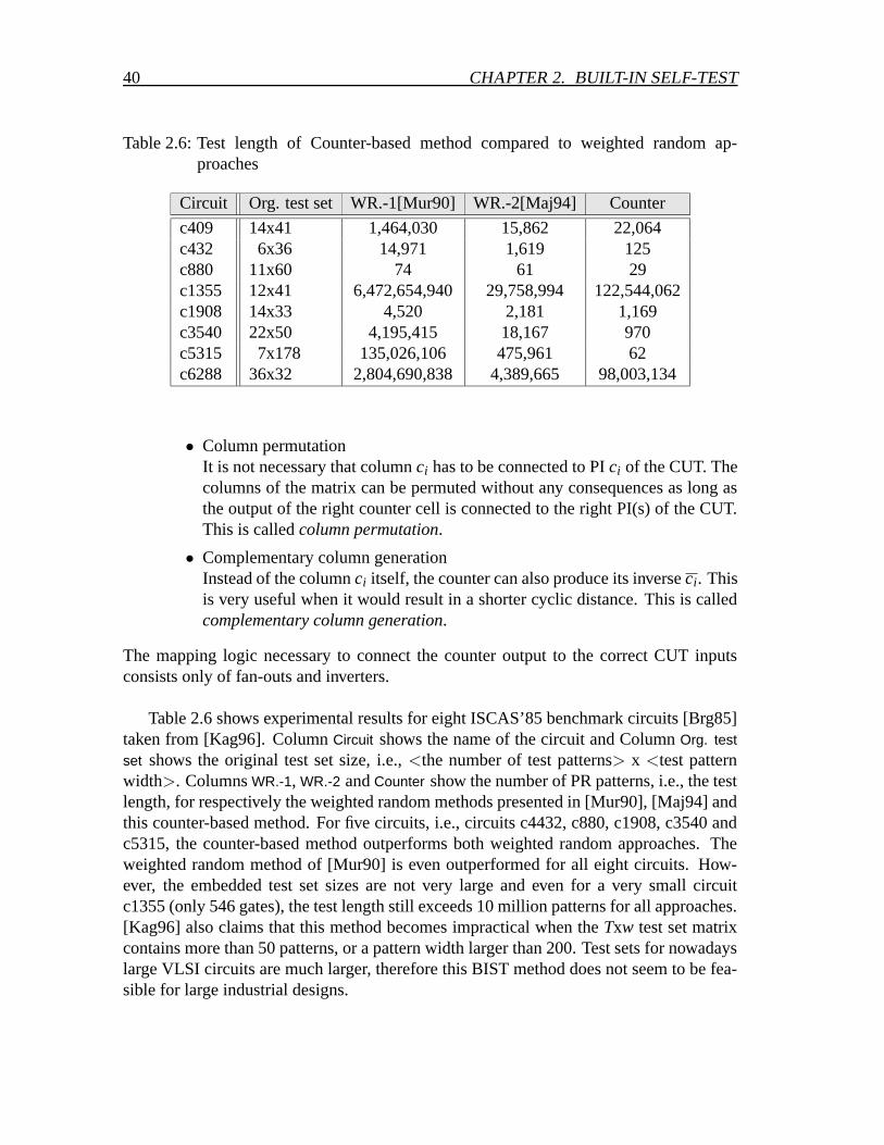
40 CHAPTER 2. BUILT-IN SELF-TEST
Table 2.6: Test length of Counter-based method compared to weighted random ap-proaches
Circuit Org. test set WR.-1[Mur90] WR.-2[Maj94] Counter
c409 14x41 1,464,030 15,862 22,064c432 6x36 14,971 1,619 125c880 11x60 74 61 29c1355 12x41 6,472,654,940 29,758,994 122,544,062c1908 14x33 4,520 2,181 1,169c3540 22x50 4,195,415 18,167 970c5315 7x178 135,026,106 475,961 62c6288 36x32 2,804,690,838 4,389,665 98,003,134
• Column permutationIt is not necessary that column ci has to be connected to PI ci of the CUT. Thecolumns of the matrix can be permuted without any consequences as long asthe output of the right counter cell is connected to the right PI(s) of the CUT.This is called column permutation.
• Complementary column generationInstead of the column ci itself, the counter can also produce its inverse ci. Thisis very useful when it would result in a shorter cyclic distance. This is calledcomplementary column generation.
The mapping logic necessary to connect the counter output to the correct CUT inputsconsists only of fan-outs and inverters.
Table 2.6 shows experimental results for eight ISCAS’85 benchmark circuits [Brg85]taken from [Kag96]. Column Circuit shows the name of the circuit and Column Org. test
set shows the original test set size, i.e., <the number of test patterns> x <test patternwidth>. Columns WR.-1, WR.-2 and Counter show the number of PR patterns, i.e., the testlength, for respectively the weighted random methods presented in [Mur90], [Maj94] andthis counter-based method. For five circuits, i.e., circuits c4432, c880, c1908, c3540 andc5315, the counter-based method outperforms both weighted random approaches. Theweighted random method of [Mur90] is even outperformed for all eight circuits. How-ever, the embedded test set sizes are not very large and even for a very small circuitc1355 (only 546 gates), the test length still exceeds 10 million patterns for all approaches.[Kag96] also claims that this method becomes impractical when the Txw test set matrixcontains more than 50 patterns, or a pattern width larger than 200. Test sets for nowadayslarge VLSI circuits are much larger, therefore this BIST method does not seem to be fea-sible for large industrial designs.

2.7. BIST FACILITATION TECHNIQUES: PARTIALLY EMBEDDED DETERMIN-ISTIC TEST PATTERNS 41
1 0 1 0 1 0 1 0 1 0 0 1 1 1 1 1 0 0 0 0
x1 x2 x3 x4 x5
Test set
x1x2x3x4x5
2−bit LFSR
c17
Figure 2.17: LFSR input reduction for ISCAS’85 circuit c17
In [Che95a] also techniques are introduced to reduce the width of the LFSR that isused to drive the PIs of the CUT. In this case no deterministic test patterns will be em-bedded; the idea is to reduce the width of the LFSR and hence the test length. Thisis achieved by shorting Compatible inputs and Inversely compatible inputs. Compatibleinputs are inputs which can be shorted together without introducing untestable faults. In-versely compatible inputs are inputs that can be shorted together by means of an inverterwithout introducing untestable faults. Fig. 2.17 shows the minimal LFSR with which IS-CAS’85 benchmark circuit c17 [Brg85] can be tested. With only a 2-bit LFSR, all faultsin circuit c17 are detected.
Table 2.7 shows experimental results taken from [Che95a] for several ISCAS’85[Brg85] and ISCAS’89 [Brg89] circuits. Column Circuit lists the circuit name and Column#Inputs shows the number of inputs (PIs and SFF outputs). The number of stages of theLFSR are shown in Column #LFSR stages.
The results listed in Table 2.7 show that the number of LFSR stages can be reducedwith a factor of 2 or even 3. For many circuits, a maximum length pattern sequence canbe generated by the LFSR (2R−1 patterns, where R is the number of LFSR stages), whilestill having a test length below the 1 million patterns (R=20). Only circuits c2670 (R=22),s838 (R=35) and s15850 (R=31) result in a maximum length sequence exceeding the 1million patterns. If a maximum length sequence is not considered feasible for a circuit,e.g., circuits s838 and s15850, still only a part of the LFSR sequence can be appliedduring test, just as in the case an LFSR is used without input reduction at the cost of alower fault coverage. The input reduction method seems to be rather complex and is CPUtime consuming (no CPU time information available) which can be a bottleneck for largeindustrial designs.
2.7.2 Fixed-biased PR BIST
The fixed-biased PR BIST architecture, presented in [Als94] is using a mixture offixed bits plus biased PR patterns. In this case biased PR patterns are patterns in whichall bits have the same probability p, 0 < p < 1, of being 1. The basic structure of this
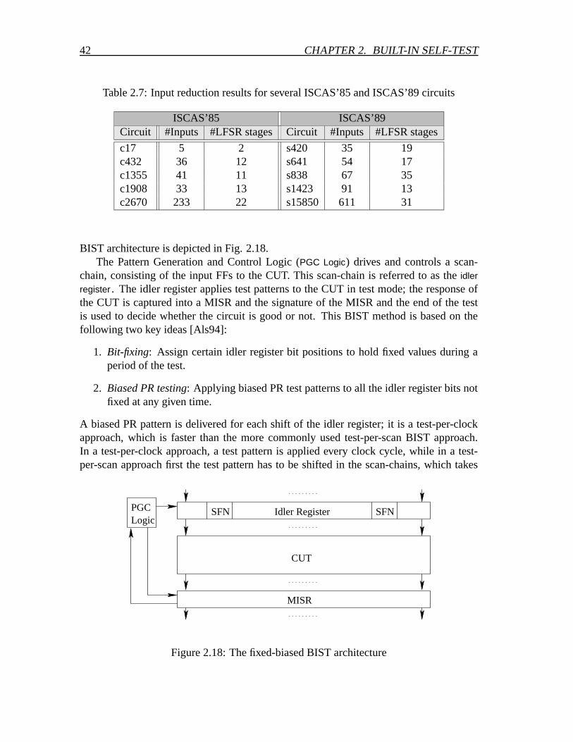
42 CHAPTER 2. BUILT-IN SELF-TEST
Table 2.7: Input reduction results for several ISCAS’85 and ISCAS’89 circuits
ISCAS’85 ISCAS’89Circuit #Inputs #LFSR stages Circuit #Inputs #LFSR stages
c17 5 2 s420 35 19c432 36 12 s641 54 17c1355 41 11 s838 67 35c1908 33 13 s1423 91 13c2670 233 22 s15850 611 31
BIST architecture is depicted in Fig. 2.18.The Pattern Generation and Control Logic (PGC Logic) drives and controls a scan-
chain, consisting of the input FFs to the CUT. This scan-chain is referred to as the idler
register . The idler register applies test patterns to the CUT in test mode; the response ofthe CUT is captured into a MISR and the signature of the MISR and the end of the testis used to decide whether the circuit is good or not. This BIST method is based on thefollowing two key ideas [Als94]:
1. Bit-fixing: Assign certain idler register bit positions to hold fixed values during aperiod of the test.
2. Biased PR testing: Applying biased PR test patterns to all the idler register bits notfixed at any given time.
A biased PR pattern is delivered for each shift of the idler register; it is a test-per-clockapproach, which is faster than the more commonly used test-per-scan BIST approach.In a test-per-clock approach, a test pattern is applied every clock cycle, while in a test-per-scan approach first the test pattern has to be shifted in the scan-chains, which takes
SFN Idler Register SFNPGCLogic
CUT
MISR
Figure 2.18: The fixed-biased BIST architecture

2.7. BIST FACILITATION TECHNIQUES: PARTIALLY EMBEDDED DETERMIN-ISTIC TEST PATTERNS 43
multiple clock-cycles (at least as many as the longest scan-chain). Bit-fixing is accom-plished by special Scan, Fix and Normal (SFN) scan-cells. These scan-cells can operatein scan, fixed-scan and normal mode. The scan and normal mode are the same as in aregular scan-cell. In the fixed-scan mode, the cells stay fixed at 1 or 0, while the value ofthe previous cell is passed to the next cell in the chain, bypassing this fixed cell.
[Als94] describes the FBIST algorithm which is used to determine the bits that have tobe fixed, the bias value and the number of different sequences (different fixed bits and/ordifferent bias values) the test will consist of. The concept of this FBIST algorithm issummarized as follows:
1. Use PR test patterns to detect the easy-to-detect faults.
2. Use an ATPG tool to generate sparsely assigned test patterns for each of the remain-ing undetected faults.
3. Use a bit selection algorithm to determine which bits, if any, need to be fixed, giventhe set of generated ATPG patterns. Use a bias determination algorithm to calculatethe appropriate bias value, and use fault simulation to evaluate the fault coverageof these fixed-biased PR test patterns. For the detected faults, remove the ATPGpatterns from the set of sparsely assigned ATPG patterns.
4. If all faults are detected: Stop; Otherwise go to step 3 with the remaining ATPGpatterns.
The bias is determined by the ratio between 1s and 0s in the sparsely assigned set of testpatterns. A bit is permanently fixed at 1(0) when all of the ATPG patterns have a 1(0) atthat position. A bit is temporary fixed at 1(0) when more than a given percentage of theATPG patterns have a 1(0) at that bit position.
The hardware overhead of the fixed-biased method consists of the extra hardwarecosts of the SFN cells and the PGC logic. According to [Als94], the SFN cells are ap-proximately 2.5 times the size of a normal scan-cell. It is therefore important that thenumber of bits that will be fixed is kept low. The PGC logic consists of:
• A ROM to store the configure sequences and the control sequences, i.e. the numberof patterns used in a configure, the bias value, the bits to fix, etc.
• A PRTPG
• Combinational logic to generate biased PR bits from the PRTPG
• A control PLA and counters which control the test operation.
Table 2.8 shows experimental results of the fixed-biased BIST method with respect tothe required test length to achieve 100% fault coverage, compared to other BIST methods[Als94]. Column Circuit shows the ISCAS’85 circuit name. Column Random T shows

44 CHAPTER 2. BUILT-IN SELF-TEST
Table 2.8: Comparison of test lengths of the fixed-biased method with other techniques
Random 3-Weight[Pom93] Fixed-biased[Als94]Circuit T T Fix Seq T Fix Seq
c432 768 1024 0 1 432 0 0c499 1216 2048 0 2 451 0 0c880 7488 8192 3 8 5280 0 0c1355 2816 4096 1 4 1599 0 0c1908 14K 4096 0 4 5148 1 1c2670 4M 58K 170 57 19K 37 4c7552 >64M 151K 207 37 191K 94 6
the required number of PR test patterns (test length) needed to detect all faults. Thefollowing six columns show respectively the number of patterns T , the number of fixedbits Fix and the number of different fixed sequences Seq for respectively the 3-Weight PRBIST method presented in [Pom93] and the fixed-biased method of [Als94].
The first five circuits are random susceptible circuits, all circuits are testable with lessthan one million PR patterns. Although the test length can be reduced by the listed BISTmethods, the reductions often do not justify the overhead of the BIST methods. The lasttwo circuits, i.e., circuits c2670 and c7552, are RPR circuits and using one of the listedBIST methods can be necessary to reduce the test length to a more acceptable level, e.g.,below 1 million patterns.
The BIST methods of [Pom93] and [Als94] have comparable results with respect tothe test length (T ) in Table 2.8. However the number of bits to fix and the number ofsequences is smaller for the method presented by [Als94].
Although the fixed-biased method is not limited to small circuits (note that for largercircuits the overhead of the PGC logic becomes relatively small), this method does notseem to be practical for RPR circuits. If a circuit is RPR, often a lot of fixed-bits andsequences have to be used to reduce the test length. As a result, the overhead of the idlerregister due to the SFN cells and the size of the PGC logic, especially the ROM-sizerequired to store all configurations, becomes unacceptable.
2.7.3 Bit-flipping BIST
In [Kie98] a BIST method is introduced which is based on flipping of bits generatedby the LFSR. This BIST system is based on the following observations [Kie98]:
1. Given a set of PR patterns, deterministic patterns can easily be embedded by modi-fying just a very small number of bits [Wun96].
2. In a PR test set only a very small number of patterns contribute to the fault coverage

2.7. BIST FACILITATION TECHNIQUES: PARTIALLY EMBEDDED DETERMIN-ISTIC TEST PATTERNS 45
GeneratingLogic(SGL)
SequenceTestControlUnit
LFSR
scan−chains
(a) Bit-flipping BIST structure
Tes
t Con
trol
Uni
t
LFSR
GS
L
Sequence ModifyingLogic (SML)
=1 =1 =1
scan−chains
(b) Sequence Generating Logic example
Figure 2.19: The Bit-flipping BIST architecture
and within these patterns only a few bits need to be specified.
3. Very often, deterministic test patterns can be clustered into a few sets such that allthe patterns of a set look very similar [Pat91].
4. Every autonomous BIST method must contain a BIST control unit containing a bitcounter and a pattern counter for generating the shift/capture signal and the “test-end”-signal.
The system is depicted in Fig. 2.19(a). It consists of an LFSR, the Sequence Generating
Logic (SGL) block and the Test Control Unit. The SGL modifies the bit sequences generatedby the LFSR at several bit positions and applies these modified sequences to the scan-chains. The structure of the SGL is depicted in Fig. 2.19(b). It consists of the Sequence
Modifying Logic (SML) and XOR (=1) gates. The current state of the LFSR, the bit counterand the pattern counter of the Test Control Unit serve as input for the SML. There theSML can overcome dependencies between LFSR outputs, no phase-shifting is required.Even a single LFSR output can be used to drive the scan-chains. However, for somecircuits this has a negative impact on the fault coverage and still multiple LFSR outputsshould be used to drive the scan-chains.
The SML is constructed iteratively. The main steps of the algorithm are described inthe following text. To reach an efficient implementation of the SML, the logic minimiza-tion routines EXPAND and REDUCE have been integrated [Bra84].
1. Check whether the current fault coverage is sufficient. If so, stop.
2. Compute the bits in the sequences that should be fixed. These are bits that shouldstay fixed because these bits are essential to detect some hard-to-detect faults. Thesefixed bits can be bits of deterministic patterns embedded during a previous iteration.

46 CHAPTER 2. BUILT-IN SELF-TEST
Table 2.9: Bit-flipping BIST silicon overhead
FE Core Scan BIST areaCircuit random area (µm2) area SGL Other Total
p4210 94.47% 113,877 12.05% 12.01% 10.58% 22.60%p4250 96.09% 97,110 8.53% 8.92% 11.95% 20.87%p8689 88.56% 217,053 10.37% 19.72% 5.69% 25.41%p8873 96.40% 289,053 7.40% 6.12% 4.14% 10.27%p13651 99.84% 308,727 8.48% 0.27% 3.91% 4.18%p14473 86.39% 333,612 9.31% 30.27% 3.87% 34.15%p27530 98.23% 542,394 3.32% 13.04% 2.32% 15.36%p44177 97.25% 1,324,980 12.38% 3.47% 0.95% 4.42%p52251 99.32% 1,482,687 14.19% 0.61% 0.88% 1.50%p52922 92.66% 1,889,622 9.34% 7.57% 0.86% 8.42%p64984 94.07% 1,714,725 14.71% 10.45% 0.70% 11.26%p80590 99.09% 2,492,622 4.94% 2.33% 0.58% 2.91%
3. REDUCE SML
4. Embed deterministic patterns. An ATPG tool is used to generate a sparsely assignedtest pattern.
5. EXPAND SML
The application of bit-flipping BIST on industrial designs is presented in [Kie00].Table 2.9, taken from [Kie00] shows bit-flipping BIST results with respect to the siliconoverhead for several Philips industrial designs. These results are obtained in case the goalwas to achieve complete fault coverage with 10,000 PR patterns. Column Circuit showsthe name of the circuit and Column FE random shows the achieved PR fault efficiencywithout bit-flipping. Column Core area and Scan area show the silicon area of the coreand the percentage of area required for making the circuit fully scannable. Column BIST
area shows the percentage of silicon area spent on the BIST logic, divided into the area ofthe SGL (SGL), the area of the remaining BIST logic, consisting of LFSR/MISR and testcontrol logic (Other), and the total percentage of silicon area spent on BIST (Total).
The results in Table 2.9 show that the area overhead for making the circuit fullyscannable is in general 5%-15%, except for circuit p27530. The percentage of area spenton the SGL differs a lot between different circuits. The size of the SGL primarily dependson the random testability of the circuit, as claimed in [Kie00]; RPR circuits, i.e., circuitsp8689, p14473, p52922, require larger SGL than more random susceptible circuits, i.e.,circuits p13651, p52251, p80590. As the LFSR, MISR and BIST test logic hardly increasewith circuit size, the percentage of silicon area spent on these logic blocks decreases withcircuit size. For the larger circuits the SGL dominates the BIST silicon overhead, as is

2.8. BIST FACILITATION TECHNIQUES: CIRCUIT MUTATION 47
shown in Column Total in Table 2.9. For circuits that are well random testable, the BISToverhead is limited, i.e., smaller than 5%, but for RPR circuits, the overhead can becomelarger than 10% up to 34% for circuit p14473. This overhead can be reduced by loweringthe required fault coverage or applying more PR patterns, as shown in [Kie00].
2.8 BIST facilitation techniques: circuit mutation
The previous sections have shown that many state-of-the-art BIST methods exist thatimprove the BIST fault coverage. However, the hardware overhead of these BIST methodsincreases for circuits that are more RPR (except for the BIST methods in Section 2.6, theirhardware overhead depends on the size of the deterministic test set they embed). For largeRPR industrial circuits, the state-of-the-art BIST methods become impractical due to toomuch hardware overhead, too low fault coverages and/or too large CPU consumption bythe BIST method’s algorithm. But when the circuits are better PR testable, the state-of-the-art BIST methods are often more promising in reaching high fault coverages with lowoverhead. If the circuits even become very PR testable, they can even be tested with anLFSR without the necessity of complex BIST implementations. This section describeshow the circuit can become better PR testable by changing the circuit, without changingits functionality.
There are two ways to make a circuit better testable:
1. Redesigning the circuit (Subsection 2.8.1)
2. Inserting test points (Subsection 2.8.2)
2.8.1 Circuit mutation: Redesigning the circuit
In case the CUT is very poorly PR testable, and all state-of-the-art BIST techniquescannot improve the PR testability without too much hardware overhead, one can considerto redesign the CUT such that it becomes better PR testable. Redesigning the circuitshould take place without changing its functionality. Redesigning the circuit impactsthe time-to-market of a CUT, because a large part of the design flow has to be doneagain, possibly in multiple iterations; e.g., verification of functionality, synthesis, timinganalysis, ATPG or BIST implementation, etc.. Therefore redesigning the circuit can beseen as a very last solution in order to improve the testability of a circuit. The necessityof redesigning a circuit can easily be avoided when circuit designers take into accountDesign-for-Test rules [Fuj85], like the BIST restrictions described in Section 2.3.
2.8.2 Circuit mutation: Inserting test points
Another way to make a circuit better testable is by inserting TPs. Instead of redesign-ing the complete circuit, extra inputs (CPs) and/or outputs (OPs) are added to make in-
48 CHAPTER 2. BUILT-IN SELF-TEST
ternal parts of the circuit better testable, without changing the remaining circuit structure.Also after TPI, parts of the design flow has to be redone; i.e., the timing analysis (to makesure that the circuit achieves its required performance), synthesis, ATPG and/or BIST im-plementation have to be redone, as is described in [Het99, Fei99, Fei01]. However theimpact on the design flow and time-to-market is limited compared to redesigning the com-plete circuit. As will be shown in the following chapters, TPI results in limited hardwareoverhead while offering significant fault coverage improvements for BIST.
2.9 Summary and conclusions
The purpose of BIST is to embed a test of a circuit on-chip in order to reduce exter-nal ATE requirements. However, due to RPR faults in the circuits, the fault coveragesachievable with BIST are often not high enough to meet the quality requirements of thesemiconductor industry. Also a successful BIST implementation implies several restric-tions on a circuit, especially with respect to three-state elements.
In order to improve BIST fault coverages, one can modify the test applied and/or mod-ify the circuit such that it becomes better testable. Several state-of-the-art BIST methodshave been described with which higher fault coverages can be achieved. These state-of-the-art BIST methods have been divided into methods that modify the test patternsgenerated by a PRTPG, methods that embed a full set of deterministic test patterns in theTPG and methods that embed parts of deterministic test patterns in the TPG.
The BIST methods that modify the generated test patterns are capable of increasingthe fault coverage. However, especially for RPR circuits, reaching higher or even com-plete fault coverage results in huge hardware overhead. The BIST methods that embeda full set of deterministic test patterns are capable of reaching complete fault coverage.Their hardware overhead depends on the size of the deterministic test set they embed.Only for circuits with a very small deterministic test set, these methods can implementBIST with affordable hardware overhead. Results on ISCAS circuits have shown that thisoverhead can become larger than the circuit itself when the deterministic test set is notsmall. The BIST methods that embed parts of deterministic test patterns can also increasethe fault coverages up to complete fault coverage. Like with the methods that modify thetest patterns, their hardware overhead increases for poorer PR-testable circuits.
When the hardware-overhead of the state-of-the-art BIST methods is too high for suc-cessful BIST implementation, one can consider redesigning the circuit to make it bettertestable. A redesign of the circuit has significant impact on the design-process and resultsin a delayed time-to-market. Instead of a complete redesign of the circuit, also TPs can beinserted to improve the testability of internal parts of the circuit. In the next two chaptersit will be shown that with TPI, also high PR fault coverages can be achieved with onlylimited hardware overhead.
CHAPTER 3
Test Point Insertion
This chapter starts with a general description of Test Point Insertion (TPI). What isTPI, what are its advantages and what are its limitations? Section 3.1 introduces test points(TPs) and Section 3.2 describes how TPI can facilitate testing. Section 3.3 describes ingeneral how TPI methods select the positions in the circuit where TPs should be inserted.Section 3.4 describes the requirements and limitations of TPI with respect to industrialdesigns. The testability analysis method COP (Controllability/Observability Program)[Brg84] is often used in TPI algorithms for determining the PR testability of faults in acircuit. Also most of the TPI algorithms for improving BIST fault coverage are basedon a STUMPS (Self-Test Using a MISR/parallel SRSG) [Bar87] architecture. Therefore,before several state-of-the-art TPI algorithms, which mainly focus on improving BISTfault coverage, are described in Section 3.7, first descriptions of COP and STUMPS aregiven in Section 3.5, respectively Section 3.6. In the following chapters, new TPI tech-niques and algorithms will be proposed. An overview of the TPI topics addressed in thefollowing chapters, including a description of the TPI benchmark circuits that have beenused to evaluate the proposed techniques and algorithms, is given in Section 3.8. Section3.9 concludes this chapter.
3.1 Test points
The key idea of TPI is to insert extra logic into the circuit such that internal signallines in the circuit will become better controllable and/or observable. This extra logic willresult in better testability of internal parts of the circuit, however it should not influencethe functionality of the circuit in normal operation mode.
Traditionally, test points (TPs) can be categorized into observation points and controlpoints. An observation point (OP) is an additional primary output which is inserted intothe circuit in order to obtain a better observability for some signal lines in the circuit. Theobservability for a signal line l is the ‘difficulty’ to propagate a value change at line l toa PO. The exact definition of ’difficulty’ depends on the used testability analysis method.
49
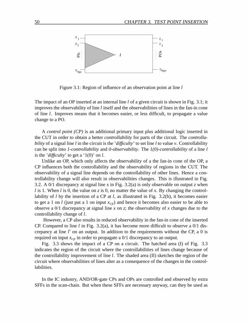
50 CHAPTER 3. TEST POINT INSERTION
z
Npi
2
1 1
2
Npoz
z
PIs
POs
x
x
x
l
Figure 3.1: Region of influence of an observation point at line l
The impact of an OP inserted at an internal line l of a given circuit is shown in Fig. 3.1; itimproves the observability of line l itself and the observabilities of lines in the fan-in coneof line l. Improves means that it becomes easier, or less difficult, to propagate a valuechange to a PO.
A control point (CP) is an additional primary input plus additional logic inserted inthe CUT in order to obtain a better controllability for parts of the circuit. The controlla-bility of a signal line l in the circuit is the ’difficulty’ to set line l to value v. Controllabilitycan be split into 1-controllability and 0-observability. The 1(0)-controllability of a line lis the ’difficulty’ to get a ‘1(0)’ on l.
Unlike an OP, which only affects the observability of a the fan-in cone of the OP, aCP influences both the controllability and the observability of regions in the CUT. Theobservability of a signal line depends on the controllability of other lines. Hence a con-trollability change will also result in observabilities changes. This is illustrated in Fig.3.2. A 0/1 discrepancy at signal line x in Fig. 3.2(a) is only observable on output z whenl is 1. When l is 0, the value on z is 0, no matter the value of x. By changing the control-lability of l by the insertion of a CP at l, as illustrated in Fig. 3.2(b), it becomes easierto get a 1 on l (just put a 1 on input xcp) and hence it becomes also easier to be able toobserve a 0/1 discrepancy at signal line x on z; the observability of x changes due to thecontrollability change of l.
However, a CP also results in reduced observability in the fan-in cone of the insertedCP. Compared to line l in Fig. 3.2(a), it has become more difficult to observe a 0/1 dis-crepancy at line l′ on an output. In addition to the requirements without the CP, a 0 isrequired on input xcp in order to propagate a 0/1 discrepancy to an output.
Fig. 3.3 shows the impact of a CP on a circuit. The hatched area (I) of Fig. 3.3indicates the region of the circuit where the controllabilities of lines change because ofthe controllability improvement of line l. The shaded area (II) sketches the region of thecircuit where observabilities of lines alter as a consequence of the changes in the control-labilities.
In the IC industry, AND/OR-gate CPs and OPs are controlled and observed by extraSFFs in the scan-chain. But when these SFFs are necessary anyway, can they be used as

3.1. TEST POINTS 51
1
&
lz
x
(a) A part of a circuit
1
1
&
ll’
xcp
xz
(b) OR gate as CP inserted at signal line l
Figure 3.2: Impact of a control point on the observability
x z
x
x
z1
2
Npi
2
1
zNpo
III
l
Figure 3.3: Regions of influence of a control point at line l
CPs and OPs themselves such that the AND/OR-gates are not necessary any longer? Thisis indeed possible, as long as transparent SFFs (TSFFS) are used, which act like buffersduring normal operation and as SFF during test mode.
Fig. 3.4 shows an example of the implementation of a transparent SFF compared tothe traditional AND/OR TPs. Fig. 3.4(a) shows the circuit part without TPs, Fig. 3.4(b)shows the circuit after the insertion of an OP at l which can be observed on output zop. Fig.3.4(c) shows the circuit after the insertion of a CP at line l which can be controlled withinput xcp. Fig. 3.4(d) shows the circuit (in test mode) after the insertion of a transparentSFF. The output of signal line l is connected with the SFF input such that l becomes fullyobservable, increasing the observabilities in the input-cone of l. The output of the SFF isconnected with signal line l’. Signal line l’ becomes controllable, like all PIs.
TSFFs have two properties different from AND/OR TPs:
1. The inserted TSFF will act as a CP and an OP at the same time; you cannot insert aCP apart from an OP. The TSFF will control the output cone of the line where it isinserted and will observe the input cone of this line.
2. TSFFs will not (lead to a) decrease (of) the observability in their fan-in cones,which is the case for AND- and OR-gate CPs. To the contrary, because a SFF TP

52 CHAPTER 3. TEST POINT INSERTION
=1& l
(a) Circuit before TPI
op&
l
=1
l’z
(b) OP at line l
cp
&
=1>=1
l
x
l’
(c) OR-gate as CP at line l
&
=1
l
l’SFF data_out
SFF data_in
(d) Transparent SFF at line l
Figure 3.4: Traditional TPs compared to the transparent SFF
x1
2
1
2
x
zz
zNpi Npo
x
l IIII
II
Figure 3.5: Regions of influence of a TSFF at line l
can observe its input, the line connected to the SFF will become fully observable.
Fig. 3.5 shows the impact of a TSFF on a circuit. Area I of Fig. 3.5 indicates the regionof the circuit where the controllabilities of lines change because of the improvement incontrollability at l due to the SFF. Area II sketches the region of the circuit where linesobservabilities alter as a consequence of the changes in the controllabilities. Area IIIindicates the region where the observability in the circuit changes due to the observabilityimprovement at l and (possibly) also due to the controllability changes.
3.2 TPI to facilitate testing
As already mentioned in Section 1.3, TPI can be used to facilitate testing by solvingtestability problems within a design. The main objective of TPI algorithms is to determine

3.3. TEST POINT SELECTION 53
which lines in a circuit are the most efficient places for inserting a TP, in order to improvethe testability and to minimize the extra silicon overhead caused by the inserted TPs. TPIcan facilitate testing in different ways. TPI can be used to:
1. facilitate pseudo-random testing:In case of on-chip testing/BIST, TPI can improve the PR testability of the RPRfaults in a circuit such that higher PR fault coverages can be achieved with fewerPR patterns. TPI methods targeted at facilitating PR testing, i.e., for BIST, are givenin Chapter 4.
2. facilitate ATPGIn case of using ATPG generated patterns, for off-chip testing or in BIST withan embedded deterministic test set, TPI can facilitate the generation of ATPG testpatterns for the faults within a circuit. TPI methods to facilitate ATPG are given inChapter 5.
TPI is not limited only to facilitate testing of stuck-at faults. In Chapter 6 it will beshown that TPI also facilitates the generation of patterns for other fault models, e.g., forgate-delay faults.
3.3 Test point selection
TPI algorithms insert TPs to improve the testability of certain (groups of) faults in thecircuit. As described in [Geu97b], the TPI algorithms can be divided into three categories,based on the method used to determine the faults which testabilities should be improved:
1. Methods that are based on ATPG
2. Methods that are based on fault simulation
3. Methods that are based on testability analysis
The ATPG based TPI algorithms use ATPG results to determine the faults for which thetestability should be improved. These are the faults for which the ATPG tool had troublegenerating a test pattern or could not even generate a test pattern. The TPI methods basedon fault simulation use the information of fault simulation on a set of (PR) test patterns toselect the set of faults of which testability should be improved.
The testability measures, e.g., COP [Brg84], SCOAP [Gol80] or test counts [Hay74],found by testability analysis, reflect the testability of a given circuit and its faults. TheTPI methods based on testability analysis use this information to select the set of faultsfor which testabilities should be improved. Determining the testability measures is lessCPU-time consuming than fault simulation, but they are less accurate than the fault sim-ulation results.
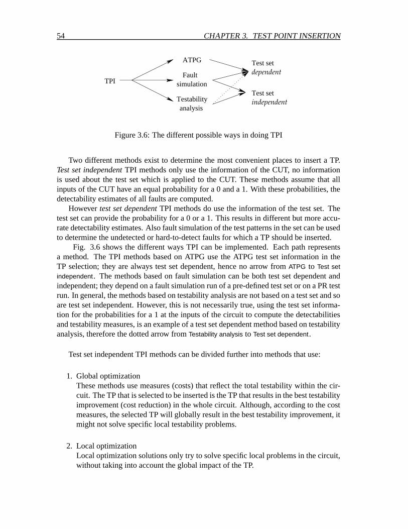
54 CHAPTER 3. TEST POINT INSERTION
TPI simulationFault
Testabilityanalysis
Test setindependent
Test setdependent
ATPG
Figure 3.6: The different possible ways in doing TPI
Two different methods exist to determine the most convenient places to insert a TP.Test set independent TPI methods only use the information of the CUT, no informationis used about the test set which is applied to the CUT. These methods assume that allinputs of the CUT have an equal probability for a 0 and a 1. With these probabilities, thedetectability estimates of all faults are computed.
However test set dependent TPI methods do use the information of the test set. Thetest set can provide the probability for a 0 or a 1. This results in different but more accu-rate detectability estimates. Also fault simulation of the test patterns in the set can be usedto determine the undetected or hard-to-detect faults for which a TP should be inserted.
Fig. 3.6 shows the different ways TPI can be implemented. Each path representsa method. The TPI methods based on ATPG use the ATPG test set information in theTP selection; they are always test set dependent, hence no arrow from ATPG to Test set
independent. The methods based on fault simulation can be both test set dependent andindependent; they depend on a fault simulation run of a pre-defined test set or on a PR testrun. In general, the methods based on testability analysis are not based on a test set and soare test set independent. However, this is not necessarily true, using the test set informa-tion for the probabilities for a 1 at the inputs of the circuit to compute the detectabilitiesand testability measures, is an example of a test set dependent method based on testabilityanalysis, therefore the dotted arrow from Testability analysis to Test set dependent.
Test set independent TPI methods can be divided further into methods that use:
1. Global optimizationThese methods use measures (costs) that reflect the total testability within the cir-cuit. The TP that is selected to be inserted is the TP that results in the best testabilityimprovement (cost reduction) in the whole circuit. Although, according to the costmeasures, the selected TP will globally result in the best testability improvement, itmight not solve specific local testability problems.
2. Local optimizationLocal optimization solutions only try to solve specific local problems in the circuit,without taking into account the global impact of the TP.

3.4. TPI FOR INDUSTRIAL CIRCUITS 55
3.4 TPI for industrial circuits
There exist many TPI algorithms [Sav91, Sei91, Che95b, Sch95, Tam96, Tou96, Tsa97],as will be described in the following sections. However, not all of these algorithms arecapable to cope with industrial circuits. E.g., Seiss [Sei91] uses equations to calculate thebest TP positions, based on the assumption that lines that are not 1, are 0. Because linesin industrial circuits can also become Z or U, the outcome of the TP selection can resultin selected TPs that do not result in better testability of the circuit. TPI can only be usedin the semiconductor industry when the TPI methods can be used in combination withindustrial circuits.
Another problem with TPI for industrial circuits are possible bus-conflicts after TPI.Circuits containing buses can be designed in such a way that bus-conflicts will never oc-cur, to avoid circuit damage and/or to implement the circuit with BIST. When TPs areinserted at wrong chosen positions, it is possible that after the insertion buses can becomein conflict, resulting in circuit damage or the inability of proper BIST insertion.
Industrial circuits also often contain embedded memories. During test, the values atthe inputs of the circuit from these embedded memories are often unknown. These un-known values propagate through the circuit resulting in poorer testability of the circuits.Test circuitry or TPs can be inserted such that these unknown inputs are bypassed andcan be controlled by the test circuitry resulting in an improvement of the testability of thecircuit.
TPs cannot be inserted at every location within an industrial design. Due to the in-sertion of a TP, the critical path1 of a design might increase. As a result, the IC has tooperate on a lower clock frequency and might not reach the performance it was originallydesigned for. TPI methods for industrial circuits should be able to exclude lines to be TPcandidate, e.g., to exclude positions that increase the critical path length of the circuit.
3.5 Controllability/Observability Program (COP)
This section describes the controllability / observability program (COP) [Brg84] thatis often used in TPI algorithms [Sav91, Sei91, Tsa97] to determine the TP positions.Section 3.5.1 introduces the COP controllability and observability values. In Section3.5.2 the equations for the controllability and observability for the in- and outputs of thestandard gates are given.
3.5.1 Introduction to COP
COP can be used to estimate the probability that a SAF will be covered by a PR pat-tern and hence determine which faults are RPR. This testability information can be used
1the path in the circuit that determines the maximum clock-frequency (performance), i.e., the path withthe longest delay

56 CHAPTER 3. TEST POINT INSERTION
by a TPI algorithm to determine where in the circuit TPs should be inserted, such that thenumber of RPR faults decreases and the overall testability of the circuit improves. COPassumes that the circuit conforms to a full-scan design.
For each signal line l in the circuit, COP provides statistical values for the controllabil-ity Cl and observability Wl of that line. In COP, the controllability (or the 1-controllability(C1l)) of a signal line l is defined as the probability that line l is 1. The 0-controllability(C0l) of a signal line l is the probability that line l is 0. In case of a Boolean circuit, if aline is not one, it is zero:
C0l +C1l = 1 (Boolean circuit)
C0l = 1−C1l (3.1)
Given a large number of PR patterns, each PI has an equal probability for a 1 and fora 0, hence the controllabilities of the PIs of the circuit are initialized at 0.5: CPI = 0.5.The controllabilities of the other signal lines are circuit dependent and their calculation isdescribed in Subsection 3.5.2.
The observability of a signal line l is defined as the probability that a value change online l will lead to a value change on at least one PO. The observability of all POs is 1:WPO = 1; the observabilities of the other lines depend on the structure of the circuit andtheir calculation is given in Subsection 3.5.2.
Compared to the description of controllability and observability as mentioned in Chap-ter 3, COP defines the difficulty to control a line as the probability the line is 1(0) anddefines the difficulty to observe a line on a PO as the probability that a value discrepancyon that line is visible on a PO.
A very large controllability of a line l, i.e., very close to 1, indicates that it is hard totest the SA1 fault on l. In that case the probability that l is 0 (required to test for the SA1fault), is very small. The opposite is true when the controllability of l is very close to 0(the 0-controllability is very close to 1). In this case it is hard to test the SA0 fault. Whenthe observability of a line l is close to 0, this means that it is very hard to propagate avalue discrepancy of line l to a PO.
A TP can be inserted to improve the 1-controllability, 0-controllability and/or observ-ability of these lines.
3.5.2 Calculation of the COP controllability and observability
Fig. 3.7 shows a 2-input AND-gate and a 2-input OR-gate. Output z of the AND-gate is only 1, when both x and y are 1. Hence, The COP controllability of the 2-inputAND-gate becomes:
Cz = Cx ·Cy (3.2)
Output z of the OR-gate is 1, when at least one of the inputs x and y is 1. Output z is0, when both x and y are 0. Hence the COP 0-controllability of the 2-input OR-gate

3.5. CONTROLLABILITY/OBSERVABILITY PROGRAM (COP) 57
& >= 1y
xx
yz z
Figure 3.7: An AND-gate and an OR-gate.
becomes:
C0z = C0y ·C0y
Rewriting in COP 1-controllabilities (assuming Boolean circuit) this results in:
Cz = 1− (1−Cx) · (1−Cy) (3.3)
A discrepancy on an input x of a gate can only be observed when the other inputsof the gate have a non-controlling value. A controlling value of a gate is a value whichforces the output of the gate to a specific value, in spite of the values of all other inputs. Inthe case of an AND-gate, the controlling value is 0, in case of an OR-gate, the controllingvalue is 1.
A value discrepancy on input x of the AND-gate in Fig. 3.7 can only be observed wheninput y has the non-controlling value 1 and output z is observable. Hence the observabilityof x becomes:
Wx = Cy ·Wz (3.4)
Input x of the OR-gate of Fig. 3.7 can only be observed when input y has the non-controlling value 0 and output z is observable. Hence the observability of input x becomes:
Wx = C0y ·Wz (3.5)
= (1−Cy) ·Wz (Boolean circuit)
These equations for COP controllability and observability can be extended for gates withmore than 2 inputs; for an L-input AND-gate the COP controllability and observabilitybecome:
Cz = Cx1 ·Cx2 · . . . ·CxL
Wx1 = Cx2 ·Cx3 · . . . ·CxL ·Wz
where x1, x2, . . ., xL are the inputs of the L-input gate and z is the output of the gate.For an L-input OR-gate the controllability and observability become:
C0z = C0x1 ·C0x2 · · ·C0xL
Cz = 1− (1−Cx1) · (1−Cx2) · · ·(1−CxL) (Boolean circuit)
Wx1 = C0x2 ·C0x3 · · ·C0xL ·Wz
Wx1 = (1−Cx2) · (1−Cx3) · · ·(1−CxL) ·Wz (Boolean circuit)

58 CHAPTER 3. TEST POINT INSERTION
Table 3.1: COP testability measures for standard gate types.
Gate Controllability Cz Observability Wx1
AND Cx1 ·Cx2 Cx2 ·Wz
NAND 1−Cx1 ·Cx2 Cx2 ·Wz
OR 1− (1−Cx1)(1−Cx2) (1−Cx2) ·Wz
NOR (1−Cx1)(1−Cx2) (1−Cx2) ·Wz
XOR Cx1 +Cx2 −2 ·Cx1 ·Cx2 Wz
NXOR 1−Cx1 −Cx2 +2 ·Cx1 ·Cx2 Wz
BUF Cx1 Wz
INV 1−Cx1 Wz
x z2
fanout stem
fanout branches
1z
zL
Cz1 = Cz2 = · · · = CzL = Cx (3.6)
Wx = 1− (1−Wz1) · (1−Wz2) · · ·(1−WzL) (3.7)
Figure 3.8: The COP measures for a fan-out stem
Table 3.1 shows the COP testability measures for standard gate elements. x1 and x2
are the gate inputs and z is the gate output. The equations in Table 3.1 are only exact whenthe values on the gate inputs are independent. This is not the case when a line fans outand reconverges further on in the circuit. This will lead to a small error in the calculationsof the COP controllabilities and observabilities.
But what does happen on a fan-out node? From the signal line, there exist multiplepaths to the POs, see Fig. 3.8. The controllabilities of the fan-out branches are equal tothe controllability of the fan-out stem. A fault on x can be observed when the fault can beobserved on at least one of the fan-out branches z1 · · ·zL and thus is only not observablewhen none of the fan-outs can be observed. The observability of the lines on the fan-outstem is the OR function of the observabilities of all fan-out branches.
The COP controllabilities and observabilities in the circuit are calculated as follows:
1. Initialize the COP controllabilities of all PIs (and SFF-outputs) to 0.5.

3.5. CONTROLLABILITY/OBSERVABILITY PROGRAM (COP) 59
2. Propagate the controllabilities from the PIs forward to the POs using the equationsgiven in the Column Controllability Cz in Table 3.1.
3. Initialize the COP observabilities of all PIs (and SFF-inputs) to 1.
4. Propagate the observabilities from the POs backward to the PIs using the equationsgiven in the Column Observability Wx in Table 3.1.
The COP controllabilities and observabilities can be combined to find the COP detec-tion probability for a given fault. The COP detection probability of SAF f on a line l is theprobability that f will be detected on a PO. A SA1 fault on a line l can only be detectedwhen l is 0 in the fault-free circuit and l is observable. The detection probability estimateof a SA1 fault can be calculated with Eq. 3.8.
Pdl/SA1 = C0l ·Wl (3.8)
= (1−Cl) ·Wl (Boolean circuit)
A SA0 fault on line l can only be detected when l is 1 in the fault-free circuit and line lis observable on a PO. The detection probability estimate of a SA0 fault can be calculatedwith Eq. 3.9.
Pdl/SA0 = Cl ·Wl (3.9)
Obviously, the larger the detection probability of a fault, the easier it is to detect this faultwith a PR pattern. The difficult faults for PR testing are the faults with a very low detectionprobability. The faults with a large detection probability will probably be detected withonly a few PR test patterns, while the RPR faults, with a low detection probability, requirea very large number of PR patterns in order to have a reasonable probability that the faultwill be covered by a test pattern.
3.5.3 Cost function and the cost gradient values
The goal of TPI for BIST is to obtain a maximal improvement in the PR testability ofa circuit with as few TPs as possible. During the selection of the TP positions, it is notadvisable to exclusively rely on the COP controllabilities and observabilities, since dueto their local nature, they are lacking the capability to analyze and describe the circuit’stestability problems from a more global point of view. For example given that line l inFig. 3.3 has a small controllability Cl . Increasing Cl will not necessarily lead to an im-provement of the circuit’s overall testability. This change may deteriorate the detectionprobabilities of several faults in the shaded area of Fig. 3.3 and may thus have a negativeimpact on the RPR testability of the circuit.
In [Lis87], a cost function (CF) is introduced, which represents the global testabilityof the circuit and the testability of individual faults. It is defined as the summation of theinverses of all COP detection probabilities. When a fault is easy to detect, its detection

60 CHAPTER 3. TEST POINT INSERTION
probability is large and the inverse is small, which means that the impact of this fault onthe cost is minimal. On the contrary, a fault with a very small detection probability has alarge inverse and thus a high impact on the cost.
The equation for the CF given in [Lis87] is:
K =1F·
F
∑f =1
K f (3.10)
K f =1
Pd f(3.11)
where K is the global cost function of the CUT, F is the number of stuck-at faults, K f
is the cost contribution of fault f , and Pd f is the detection probability of a fault f inthe CUT. A large circuit, with many faults, is not necessarily harder to test than a smallcircuit, with fewer faults. To compensate the CF for the number of faults in the CUT, theCF is multiplied with 1
F . However, many TPI algorithms that use this CF [Sei91, Tsa97]ignore the 1
F factor and use Eq. 3.12.
K =F
∑f =1
K f (3.12)
For every signal line l in the CUT, two SAFs exist, e.g., the SA0 and SA1 fault.Therefore Eq. 3.10 can also be written as Eq. 3.13.
K =1
2L·
L
∑l=1
(Kl/SA0 +Kl/SA1
)(3.13)
=1
2L·
L
∑l=1
(
1Pdl/SA0
+1
Pdl/SA1
)
where L is the total number of signal lines in the CUT and l/SA0 and l/SA1 represent linel SA0, respectively SA1. Ignoring the 1
2L factor, Eq. 3.13 becomes:
K =L
∑l=1
(Kl/SA0 +Kl/SA1
)(3.14)
=L
∑l=1
(
1Pdl/SA0
+1
Pdl/SA1
)
[Lis87] also introduces the cost gradient values. They are used to estimate the impactof controllability and observability changes of a line line on the rest of the circuit. Foreach line, two gradient values are defined, namely dK
dCland dK
dWl. They are the derivatives
of the CF K with respect to the 1-controllability, respectively the observability, of line l

3.5. CONTROLLABILITY/OBSERVABILITY PROGRAM (COP) 61
and are called the controllability gradient and the observability gradient of line l.Both gradient values are still not very good indicators of the global testability impact
after the insertion of a TP, because they represent the change rate of K to Cl and Wl
respectively due to an infinitely small change of Cl and Wl , whereas the insertion of a TPmay cause Cl or Wl to change drastically. Although the gradients are not very accuratethemselves, they still can be useful in determining good TP positions, as will be shown inSection 3.7. How to calculate the gradient values is described in the following text.
Calculation of the gradient values
Changing a line’s observability only affects the detection probabilities of its predeces-sors, see Fig. 3.1. Therefore a change in the observability of PI x affects only the detectionprobability of the input itself and so only two terms of the global cost function; the termwith respect to the SA0 fault, respectively the SA1 fault, on input x. The derivative of theCF with respect to a change in PI observability of input x becomes:
dKdWx
=dKx/SA0
dWx+
dKx/SA1
dWx(3.15)
In case Eq. 3.11 is used for the cost contribution for a fault, Eq. 3.15 becomes:
dKdWx
=d( 1
Pdx/SA0)
dWx+
d( 1Pdx/SA1
)
dWx=
d( 1Cx·Wx
)
dWx+
d( 1(1−Cx)·Wx
)
dWx
=−Cx
(Cx ·Wx)2 +Cx −1
((1−Cx) ·Wx)2 =−Cx
Pd2x/SA0
+Cx −1
Pd2x/SA1
(3.16)
Given a gate with X inputs and one output, changing the observability on the gate outputz also results in observability changes on the gate inputs, because the observabilities onthe gate inputs depend on the observability at the gate output (see Column Observability
Wx in Table 3.1). Thus the CF will not only change by the two terms with respect tothe SA0 and SA1 fault of output z, but also by the observability changes on the X gateinputs. Since it is known how the cost changes with respect to the observability on thesegate inputs, it is possible to apply a chain-rule to compute the derivative with respectto observability changes on the gate output z. The derivative of the CF with respect toobservability changes on the gate output z is given in Eq. 3.17, where xi represents the ithinput of the gate.
dKdWz
=dKz/SA0
dWz+
dKz/SA1
dWz+
X
∑i=1
dKdWxi
dWxi
dWz(3.17)
In case Eq. 3.11 is used as cost contribution for a fault, Eq. 3.17 can be written as:
dKdWz
=−Cz
Pd2z/SA0
+(Cz −1)
Pd2z/SA1
+X
∑i=1
dKdWxi
dWxi
dWz(3.18)

62 CHAPTER 3. TEST POINT INSERTION
The first two terms of Eq. 3.17 are due to the observability changes on output z itself,and the summation is due to the observability changes on the X inputs of the gate. Thequantities dWxi/dWz depend on the gate type and represent a transfer function that dictateshow a gate’s input observability will change, given a change in output observability. Theycan be calculated from the gate observability equations given in Table 3.1.
After the computation of dK/dW for all signal lines in the CUT, the dK/dC values,which depend on dK/dW , can be determined. Because changing a gate’s input controlla-bility affects both the output controllability and the observability of the other gate inputs(see Fig. 3.3), the chain-rule equation for dK/dC is slightly more complicated than for thedK/dW forward propagation. However, changing the controllability on a PO only influ-ences the cost contribution for the SA0 and SA1 faults on that PO. The derivative of theCF K with respect to a controllability change on PO z is:
dKdCz
=dKz/SA0
dCz+
dKz/SA1
dCz(3.19)
And using Eq. 3.11 as cost contribution for a fault, Eq. 3.19 becomes:
dKdCz
=d( 1
Pdz/SA0)
dCz+
d( 1Pdz/SA1
)
dCz=
−Wz
Pd2z/SA0
+Wz
Pd2z/SA1
(3.20)
The two terms in Eq. 3.20 represent the cost change caused by the the SA0 and SA1detectabilities changes on PO z. Propagation of dK/dC proceeds in backward direction,beginning with initialized POs, according to the following equation:
dKdCx j
=dKx j/SA0
dCx j
+dKx j/SA1
dCx j
+X
∑i=1,i6= j
dKdWxi
dWxi
dCx j
+Z
∑k=1
dKdCzk
dCzk
dCx j
(3.21)
where X are the number of inputs of the gate, Z the number of outputs, xi and x j are thegate inputs and zk are the gate outputs. Using Eq. 3.11 as cost contribution for a fault, Eq.3.21 becomes:
dKdCx j
=−Wx j
Pd2x j/SA0
+Wx j
Pd2x j/SA1
+X
∑i=1,i6= j
dKdWxi
dWxi
dCx j
+Z
∑k=1
dKdCzk
dCzk
dCx j
(3.22)
The first two terms calculate the cost impact of controllability changes at line x j itself.The third term, the summation over all other inputs of the gate, gives the cost impact ofthe observability changes on these other inputs due to the controllability change on inputx j. The last term, the summation over all outputs, gives the cost impact of the control-lability changes on the gate outputs due to the controllability changes on input x j. ThedWxi/dCx j and dCzk /dCx j values, which represent the observability change at input xi, re-spectively controllability change on output zk given the controllability change on x j, can

3.6. STUMPS 63
Algorithm 3.1 COP gradients calculationInput: CUT, C and W for all lines in CUTOutput: COP gradients for all lines in CUT
for all PIs ∈ CUT doInitialize dK/dW with Eq. 3.16.
for all Lines ∈ CUT from PIs to POs doCompute dK/dW for all other lines by applying Eq. 3.18 to all gates in the circuit asingle forward pass.
for all POs ∈ CUT doInitialize dK/dC with Eq. 3.20.
for all Lines ∈ CUT from POs down to PIs doCompute dK/dC for all other lines by applying Eq. 3.22 to all gates in a singlebackward pass.
be derived from the equations listed in Table 3.1.
The complete gradients calculation procedure is given in Algorithm 3.1. This pro-cedure is linear in the number of gates in the CUT, since the equations are applied on agate-by-gate basis.
3.6 STUMPS
In this dissertation, it is assumed that the circuit uses the popular STUMPS approachin case of PR BIST. STUMPS is an abbreviation for Self-Test Using MISR / ParallelSRSG; where SRSG stands for Shift Register Sequence Generator, see [Bar87]. Origi-nally, STUMPS was a BIST architecture for an LSSD (Level Sensitive Scan Design)-basedmulti-chip system, in which each Field Replaceable Unit (FRU) contains a large numberof logic chips. But the STUMPS model can also be used in a single chip design, it isjust a different scale; the circuit represents the FRU and the different scan-chains in thecircuit represent the large number of logic chips. This section describes the properties ofSTUMPS and how it can be adapted for PR BIST.
3.6.1 Introduction to STUMPS
The STUMPS architecture often used in PR BIST is depicted in Fig. 3.9. STUMPSBIST is a full-scan BIST method. It is assumed that the FFs of the circuit core are con-nected into multiple scan-chains (scan-chain). The PRTPG (implemented by means of anLFSR or CA) applies PR test patterns to the core by shifting the scan-chains. While thenew patterns are shifted into the chains by the LFSR/CA, the output of the scan-chains
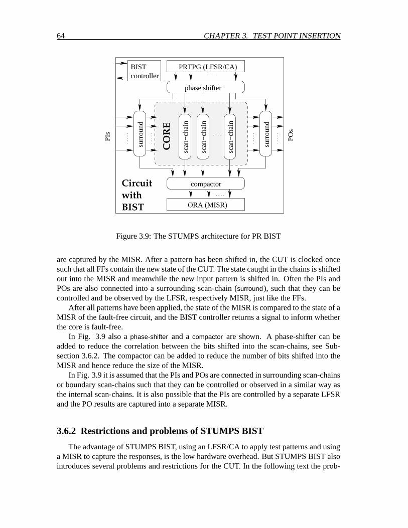
64 CHAPTER 3. TEST POINT INSERTION
PRTPG (LFSR/CA)
ORA (MISR)
compactor
controllerBIST
Circuit
BISTwith
phase shifter
PIs
POs
CO
RE
scan
−ch
ain
scan
−ch
ain
scan
−ch
ain
surr
ound
surr
ound
Figure 3.9: The STUMPS architecture for PR BIST
are captured by the MISR. After a pattern has been shifted in, the CUT is clocked oncesuch that all FFs contain the new state of the CUT. The state caught in the chains is shiftedout into the MISR and meanwhile the new input pattern is shifted in. Often the PIs andPOs are also connected into a surrounding scan-chain (surround), such that they can becontrolled and be observed by the LFSR, respectively MISR, just like the FFs.
After all patterns have been applied, the state of the MISR is compared to the state of aMISR of the fault-free circuit, and the BIST controller returns a signal to inform whetherthe core is fault-free.
In Fig. 3.9 also a phase-shifter and a compactor are shown. A phase-shifter can beadded to reduce the correlation between the bits shifted into the scan-chains, see Sub-section 3.6.2. The compactor can be added to reduce the number of bits shifted into theMISR and hence reduce the size of the MISR.
In Fig. 3.9 it is assumed that the PIs and POs are connected in surrounding scan-chainsor boundary scan-chains such that they can be controlled or observed in a similar way asthe internal scan-chains. It is also possible that the PIs are controlled by a separate LFSRand the PO results are captured into a separate MISR.
3.6.2 Restrictions and problems of STUMPS BIST
The advantage of STUMPS BIST, using an LFSR/CA to apply test patterns and usinga MISR to capture the responses, is the low hardware overhead. But STUMPS BIST alsointroduces several problems and restrictions for the CUT. In the following text the prob-

3.6. STUMPS 65
lems for STUMPS BIST are briefly discussed and possible solutions are mentioned.
The problems in a STUMPS BIST environment are:
1. Lower fault coverage caused by RPR faults.LFSRs and CAs often fail to detect the RPR faults. Therefore, the fault coveragesthat can be obtained with STUMPS BIST are often low for circuits which sufferfrom many RPR faults.
The fault coverage can be increased by applying more PR test patterns, but moretest patterns means longer test times and, given a reasonable number of test pat-terns/test time, the obtained fault coverages are still too low. However, the insertionof TPs to improve the PR detectabilities in the circuit will result in an increasedfault coverage.
2. Lower fault coverage caused by correlation between the patterns shifted into thedifferent scan-chainsLFSRs which feed multiple scan chains in parallel can result in lower fault cov-erages due to structural dependencies introduced by the TPG [Raj99]. When thescan-chains are fed directly from adjacent stages in the LFSR, the chains will con-tain highly correlated patterns; the difference between the patterns is that they areonly shifted one bit. For example, the first chain will contain the pattern 10011001while the second one contains pattern 00110010.
This problem can be solved by adding a Phase Shifter [Raj99] (or XOR cloud)between the LFSR/CA and the scan-chains.
3. Unknown MISR states caused by unknown/fixed input valuesIt is possible that several inputs of the CUT have an unknown/fixed value, e.g.,inputs from an embedded memory. These unknown values result in paths withunknowns in the CUT and can finally propagate to one or several outputs (the prop-agation of unknowns is also called X-path propagation). When an unknown valueis captured into a MISR, the complete state of the MISR cannot be determined andwith an unknown MISR state, it cannot be checked whether a CUT is fault-free ornot.
This problem can be solved by the insertion of additional logic/TPs such that,in test mode, these unknown values are replaced by known, fixed or PR values.Another solution is to insert additional logic at the outputs which capture unknownstates and map them to known states.
4. Possible circuit damage and unknown MISR states caused by bus-conflictsWith ATPG one can avoid bus-conflicts. The ATPG just generates patterns suchthat all buses are only driven by at most one driver. But this is not the case for PRpatterns; it is possible that some buses are driven by multiple drivers. This resultsin bus-conflicts that can damage the circuit. These conflicts also result in unknownvalues that can propagate into the MISR, corrupting the MISR state.

66 CHAPTER 3. TEST POINT INSERTION
There are three general solutions for this problem:
(a) Insert additional logic in the circuit such that for all patterns, no bus is drivenby multiple drivers at the same time.
(b) Insert additional logic between the PRTPG and the original circuit such thatonly patterns are shifted into the scan-chains that will not result in bus-conflicts.
(c) Do not prevent the bus-conflicts (can result in circuit-damage), but insert ad-ditional logic between the outputs of the circuit and the MISR such that allpossible unknowns are mapped into known values such that the MISR state isknown for the fault-free case.
3.7 State-of-the-art TPI algorithms
In this section, several state-of-the-art TPI algorithms will be described. Subsection3.7.1 describes the Cost Reduction Factor (CRF) algorithm. This algorithm calculatesfor each TP candidate an estimate for the reduction in the global test cost of the circuit.Subsection 3.7.2 describes an algorithm which calculates a more accurate estimate forthe reduction in cost for each TP candidate; the Hybrid Cost Reduction Factor (HCRF).Subsection 3.7.3 describes a TPI algorithm that splits the test into multiple phases. In eachphase a different set of TPs will be enabled. Subsection 3.7.4 gives a short description ofseveral other TPI algorithms found in literature.
3.7.1 The Cost Reduction Factor (CRF) TPI algorithm
In [Sei91], an O(n) algorithm is described which calculates an estimate for the reduc-tion in cost that a TP candidate would cause. This estimate is called the Cost ReductionFactor (CRF). The CRF for a given signal line that will be TP candidate, is calculated byusing only local testability information of that line, i.e., the COP controllability, observ-ability and gradient values. Therefore the CRF for all TP candidates can be calculatedvery fast, while the calculation of the Actual Cost Reduction Factor (ACRF) for all TPcandidates would be very CPU-consuming. The ACRF of a TP candidate is obtained bytemporarily inserting the TP into the circuit, re-evaluating the CF and determining theACRF value by subtracting the new cost value from the old one. This is an O(n2) algo-rithm, i.e., for each n TP candidates (assuming all lines in the circuit can be TP candidate)in the circuit, a TP is inserted after which for all n lines in the circuit the cost is recalcu-lated.
In Seiss et al. [Sei91], the CRFs for AND-gate CPs, OR-gate CPs and OPs are de-rived. The CRFs for a CP at line l for an AND respectively and OR gate are given in Eqs.3.23 and 3.24.
CRFANDl =
1−Cl
2−Cl·Cl ·
dKdCl
−2
Cl · (1−Cl) ·Wl(3.23)
3.7. STATE-OF-THE-ART TPI ALGORITHMS 67
CRFORl =
Cl −1Cl +1
·Cl ·dKdCl
−2
Cl · (1−Cl) ·Wl(3.24)
The CRF for an OP at line l, derived in [Sei91], is given in Eq. 3.25:
CRFOPl = (Wl −1) ·Wl ·
dKdWl
if line l represents a fan-out stem in the original circuit
CRFOPl = (Wl −1) ·Wl ·
dKdWl
−
(1Cl
+1
1−Cl
)
otherwise (3.25)
The distinction between line l representing a fan-out stem or not can be explained by con-sidering Fig. 3.4.a and 3.4.b. In the case that line l is not a fan-out stem in the originalcircuit, the introduction of the additional fan-out branch, which is required to implementthe OP, causes line l to become a fan-out stem in the modified circuit. As a consequence,two new faults have to be modeled, which are the SA0 and SA1 faults for the newly cre-ated fan-out stem. Since these two faults are observable on the new PO with observability1, their contribution to the cost and CRFObs
l is given by 1/Cl + 1/(1-Cl). When l alreadydenotes a fan-out stem in the original circuit, no new faults have to be modeled.
The CRFs, however, could differ significantly from the ACRFs, for the followingreasons:
1. The observability changes due to a CP are completely ignored. This means that theobservability changes of lines in the fan-in cone of POs, reachable from the CP, arecompletely neglected.
2. Certain circuit structures and fault sets were assumed during the derivation of theCRF equations. By assuming that CUTs contain these types of structures, a con-trollability value Cl can be factored out such that the rest of the terms in K arecompletely independent to Cl . This assumption is not generally true.
The CRF TPI algorithm of Seiss et al. [Sei91] is listed in Algorithm 3.2. In eachiteration of the outermost while loop, the algorithm inserts exactly one CP or OP into thecircuit. TPs are inserted until the cost K of the circuit reaches a desired cost (Kdesired),or the number of inserted TPs (#TPs) has reached the maximum number of TPs (#TPmax)that are allowed to be inserted. Because the controllability, observability, controllabilityand observability gradients, and the CRFs may have changed due to the insertion of theTP, these values have to be updated at the beginning of each iteration. Subsequently, thealgorithm selects a set of candidate lines for TPI by exploiting the CRFs as a guidance.The CRFs are not very accurate and as described in [Tsa97], the inaccuracy of the CRFsbecomes more significant when a high fault coverage is reached. Therefore, the CRF isonly used to pre-select a small number of possible TPs in the CRF TPI algorithm. TheACRFs are only calculated for the pre-selected lines. This saves a lot of time because

68 CHAPTER 3. TEST POINT INSERTION
Algorithm 3.2 CRF Test Point InsertionInput: CUT, desired cost (KKKdesired), TTT PPPmax
Output: CUT with TPs
while ( KKK > KKKdesired) and (#TTT PPPsss < #TTT PPPmax) dofor all lines lll ∈ CUT do
Evaluate controllability CCCl and observability WWW l
Compute the gradients dKKK/dWWW l and dKKK/dCCCl
Compute CCCRRRFFFOPl
if (dKKK/dCCCl < 0) thenCompute CCCRRRFFFOR
lelse
Compute CCCRRRFFFANDl
Determine CCCRRRFFFCPmax with ∀lll∈CUT(CCCRRRFFFAND/ORl <= CCCRRRFFFCPmax)
Determine CCCRRRFFFOPmax with ∀lll∈CUT(CCCRRRFFFOPl <= CCCRRRFFFOPmax)
Determine the set SSSLLLCP of all lines lll ∈ CUT withSSSLLLCP = {lll |CCCRRRFFFAND/OR
l > 0.1 ·CCCRRRFFFCPmax}Determine the set SSSLLLOP of all lines lll ∈ CUT with
SSSLLLOP = {lll |CCCRRRFFFOPl > 0.1 ·CCCRRRFFFOPmax}
NNNRRR = 1for all lines lll ∈ SSSLLLCP do
if (dKKK/dCCCl < 0) thenSimulation of an OR type CP at line lll
elseSimulation of an AND type CP at line lll
Evaluation of cost function KKKm for the modified CUTcccooosssttt[NNNRRR] = KKKm
NNNRRR = NNNRRR+1for all lines lll ∈ SSSLLLOP do
Simulation of an OP at line lllEvaluation of cost function KKKm for the modified CUTcccooosssttt[NNNRRR] = KKKm
NNNRRR = NNNRRR+1Select line lllT P with ∀0<lll<=NNNRRR(cccooosssttt[lll]) >= cccooosssttt[lllT P])if (lllT P ∈ SSSLLLCP) then
if (dKKK/dCCClT P < 0) thenInsert an OR type CP at line lllT P
elseInsert an AND type CP at line lllT P
elseInsert an OP at line lllT P
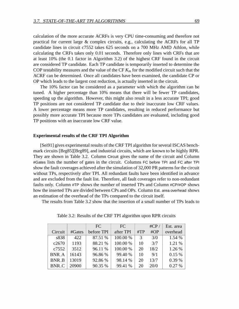
3.7. STATE-OF-THE-ART TPI ALGORITHMS 69
calculation of the more accurate ACRFs is very CPU time-consuming and therefore notpractical for current large & complex circuits, e.g., calculating the ACRFs for all TPcandidate lines in circuit c7552 takes 625 seconds on a 700 MHz AMD Athlon, whilecalculating the CRFs takes only 0.01 seconds. Therefore only lines with CRFs that areat least 10% (the 0.1 factor in Algorithm 3.2) of the highest CRF found in the circuitare considered TP candidate. Each TP candidate is temporarily inserted to determine theCOP testability measures and the value of the CF Km for the modified circuit such that theACRF can be determined. Once all candidates have been examined, the candidate CP orOP which leads to the largest cost reduction, is actually inserted in the circuit.
The 10% factor can be considered as a parameter with which the algorithm can betuned. A higher percentage than 10% means that there will be fewer TP candidates,speeding up the algorithm. However, this might also result in a less accurate TPI; goodTP positions are not considered TP candidate due to their inaccurate low CRF values.A lower percentage means more TP candidates, resulting in reduced performance butpossibly more accurate TPI because more TPs candidates are evaluated, including goodTP positions with an inaccurate low CRF value.
Experimental results of the CRF TPI Algorithm
[Sei91] gives experimental results of the CRF TPI algorithm for several ISCAS bench-mark circuits [Brg85][Brg89], and industrial circuits, which are known to be highly RPR.They are shown in Table 3.2. Column Circuit gives the name of the circuit and Column#Gates lists the number of gates in the circuit. Columns FC before TPI and FC after TPI
show the fault coverages achieved after the simulation of 32,000 PR patterns for the circuitwithout TPs, respectively after TPI. All redundant faults have been identified in advanceand are excluded from the fault list. Therefore, all fault coverages refer to non-redundantfaults only. Column #TP shows the number of inserted TPs and Column #CP/#OP showshow the inserted TPs are divided between CPs and OPs. Column Est. area overhead showsan estimation of the overhead of the TPs compared to the circuit itself.
The results from Table 3.2 show that the insertion of a small number of TPs leads to
Table 3.2: Results of the CRF TPI algorithm upon RPR circuits
FC FC #CP / Est. areaCircuit #Gates before TPI after TPI #TP #OP overhead
s838 422 87.51 % 100.00 % 3 3/0 1.54 %c2670 1193 88.21 % 100.00 % 10 3/7 1.21 %c7552 3512 96.11 % 100.00 % 20 18/2 1.26 %
BNR A 16143 96.86 % 99.40 % 10 9/1 0.15 %BNR B 13019 92.86 % 98.14 % 20 13/7 0.39 %BNR C 20900 90.35 % 99.41 % 20 20/0 0.27 %

70 CHAPTER 3. TEST POINT INSERTION
Table 3.3: Estimated detection probabilities of the hardest-to-detect faults end the testlength required to achieve 99% fault coverage, before and after TPI.
Pd f hardest- Pd f hardest- Test length Test lengthCircuit to-detect faults to-detect faults 99 % FC 99 % FC
before TPI after TPI before TPI after TPIs838 3.36·10−11 2.57·10−04 > 10 000 000 2 000
c2670 3.47·10−06 2.38·10−04 420000 1 200c7552 1.42·10−13 4.26·10−05 8900000 1 800
BNR A 6.03·10−11 1.33·10−06 > 10000000 21 000BNR B 1.86·10−09 5.27·10−06 6 400000 36 000BNR C 2.16·10−19 2.48·10−06 > 10000000 7 300
a significant increase of the fault coverage achievable with 32,000 random patterns, e.g.,by inserting only 3 TPs in circuit s838, the fault coverage has increased with 13% from87% to 100%. For the remaining circuits, the increase in fault coverage ranges from 4% to12%, after the insertion of only 10 to 20 TPs. The results also show that the estimated areaoverhead is in the order of 1% for all circuits, and even smaller for the larger, industrialcircuits. The area-overhead estimates do take in account the additional SFFs, which haveto be inserted in the scan-chain in order to feed the CPs and to capture the test responsesat the OPs.
Because they are good indicators for the random pattern testability of a circuit, thedetection probabilities of the hardest-to-detect faults for the circuits listed in Table 3.2 aregiven in Table 3.3. Another criterion characterizing the random pattern testability of a cir-cuit consists of the test length required to achieve a certain fault coverage. Table 3.3 alsolists the test length which is necessary to achieve a fault coverage of 99%. Columns Pd f
hardest-to-detect faults before TPI, respectively after TPI, show the lowest detection proba-bility found in the circuit before TPI, respectively after TPI. Columns Test length 99% FC
before TPI, respectively after TPI, show the number PR patterns that are applied until the99% fault coverage level has been reached before TPs, respectively after TPs, have beeninserted. The results show that the detection probability of the hardest-to-detect faults inthe modified circuits are improved by several orders of magnitude, compared to the onesof the original circuits; e.g., the detection probability of the hardest-to-detect fault in cir-cuit c7552 has been improved by 8 orders of magnitude from 1.42 ·10−13 to 4.26 ·10−5.In circuit BNR C the improvement even is 13 orders of magnitude, from 2.16 · 10−19 to2.48 ·10−6.
Before TPI, all circuits listed in Table 3.3 require far more than 32,000 PR patternsbefore the 99% fault coverage level is reached, ranging from 420,000 patterns for circuitc2670 to more than 10 million patterns for circuits s838, BNR A and BNR C. After TPI,all circuits can be tested with less than 32,000 PR patterns, except circuit BNR B which

3.7. STATE-OF-THE-ART TPI ALGORITHMS 71
requires 36,000 PR patterns. But even the test length for circuit BNR B after TPI is only36,000/6,400,000=0.56% of the test length required without TPs. The test time is propor-tional with the test length, hence the same reduction in test time is achieved by the TPI.
That the CRF TPI algorithm can be used in combination with a BIST method, i.e.,bit-flipping BIST [Kie98] described in Subsection 2.7.3, to facilitate the BIST method inreaching higher fault coverages with less silicon overhead, is shown in [Vra02].
CRF TPI derived algorithms
In Cheng et al. [Che95b], the CRF TPI algorithm has been adjusted such that it canalso be applied to partial-scan circuits, i.e., circuits that contain both scannable as non-scannable flipflops. The CRF based TPI algorithm of [Che95b] also takes into accounttiming information, such that TPs are not inserted at critical paths.
In Nakao et al. [Nak99], also a CRF based TPI algorithm for BIST is presented. Inorder to reduce the delay of the TPI, TPs (CPs) are only inserted at inverters and bufferpositions. Buffers/inverters are replaced by AND/OR gates controlled by SFFs whichmust provide a non-controlling value during normal application mode. Also the OPs areimplemented by means of SFFs. If possible, SFFs that control or observe the TPs, areshared in order to minimize the hardware overhead.
3.7.2 The Hybrid Cost Reduction Factor (HCRF) TPI algorithm
This section describes a TPI algorithm presented by Tsai et al. [Tsa97]. It uses theHybrid Cost Reduction Factor (HCRF) for estimating the Actual Cost Reduction Factor.The key idea of the HCRF TPI algorithm is that an event-driven mechanism is used topropagate the testability changes due to a TP. Once the changes become small, the gradi-ents (see Section 3.5.3) can be used to estimate the testability changes of all other lines toavoid high computational complexity of recalculating the testabilities for the entire circuit.
The CRFs can deviate significantly from the ACRFs, especially when the circuit has ahigh fault coverage [Tsa97]. Therefore, the CRF Test Point Selection algorithm presentedin the previous section only uses the CRF values as a guidance to select the best TP toinsert. However, the ACRF values still have to be calculated for the limited set of possibleTPs, which remains after the pre-selection based on the highest CRF values. When theset of candidate TPs is too small, the number of calculations and the CPU time necessaryis limited, but it is very well possible that several good TPs are excluded because theirCRF values are not accurate. On the other hand, a larger set of candidate TPs means morecalculations and possibly impractical CPU consumption.
With the HCRF TPI algorithm, it is not necessary to do a pre-selection on all TP can-didates and to calculate the ACRF for all pre-selected candidates, by temporarily insertingthe TP. Only the HCRF estimates from all TP candidates are used to select the TP that

72 CHAPTER 3. TEST POINT INSERTION
will be inserted. Before the HCRF calculation, and the TPI algorithm based on the HCRF,are explained, first the relation between the ACRF and the HCRF is given.
Given a fault set F, the ACRF for a TP can be expressed by:
ACRF = K(Org)−K(m)
= ∑f∈F
(
1
Pd f(Org)
−1
Pd f(m)
)
(3.26)
= ∑f∈F1
(
1
Pd f(Org)
−1
Pd f(m)
)
︸ ︷︷ ︸
the difference is large
+ ∑f∈F2
(
1
Pd f(Org)
−1
Pd f(m)
)
︸ ︷︷ ︸
the difference is small
where K(Org), K(m) are the cost values, and Pd f(Org), Pd f
(m) the detection probabilities offault f, before, respectively after, the modification of the circuit by the inserted TP (can-didate). The fault set F can be divided into two subsets, F1 and F2. For each fault in F1,
1Pd f
(Org) −1
Pd f(m) is large and therefore the gradient approximation is not accurate. On the
other hand, for every fault in F2, the difference of 1Pd f
(Org) and 1Pd f
(m) is small enough such
that the gradients can accurately enough estimate their impact on K, see Subsection 3.5.3.Typically, the size of F1 is much smaller than that of F2, because the test only influ-
ences a small part of the circuit. Therefore, 1Pd f
(Org) −1
Pd f(m) can be calculated explicitly
for faults in F1 (by computing 1Pd f
(m) ) and the gradients can be used to evaluate the sec-
ond term of Eq. 3.26. An event-driven mechanism is used to propagate the controlla-bility/observability changes caused by the TP candidate until the changes drop below athreshold. Whether an event at line lF1 is scheduled for further propagation is determinedby the ratio of dK/dWlF1
·∆WlF1to K(Org). The change in observability of line lF1 is rep-
resented by ∆WlF1. The region of lines processed to identify set F1 is relatively very small
for a large design, therefore the complexity for calculating the first term of Eq. 3.26 islow. In addition, gradients can provide a very good estimate for the second term of Eq.3.26, because the assumptions of the gradients are not violated for faults in F2. How tocalculate the HCRF for OPs, respectively CPs, is given in the following text.
Calculation of the HCRF for OPs
The propagation of the explicit recalculation of the COP observability changes of faultset F1 starts from the OP l backward to the PIs, shown in Fig. 3.10. For each gate outputzgate inside Region I, the gradient approximation, i.e., the ratio of dK/dWzgate ·∆Wzgate toK(Org), is larger than a given (user-defined) threshold. As a result, the event-driven mech-anism continues with the explicit recalculation of the COP observabilities of the gateinputs. Propagation of the explicit recalculation stops when the gradient approximationbecomes below the user-defined threshold, illustrated in Fig. 3.10 by the Boundary line.

3.7. STATE-OF-THE-ART TPI ALGORITHMS 73
Observation pointx
xNPI
1
lI
Boundary line
II
Z
Z
NPO
1
Figure 3.10: Computing HCRF for an OP
At the Boundary line, the gradient approximation is used to estimate the cost impact ofthe observability changes of the faults in Region II.
The HCRF for an OP comprises three parts:
1. ∑ f
(
1Pd f
(Org) −1
Pd f(m)
)
for every fault f inside Region I; the new observabilities and
therefore the new Pd f ’s are computed explicitly.
2. For all faults inside Region II, ∑lbounddK
dWlbound·∆Wlbound , where lbound’s are the lines
on the boundary in Fig. 3.10, is used to estimate their contribution to the ACRF.
3. If the OP l is not a fan-out stem in the original circuit, the contribution of the newfan-out branch faults ( 1
Pdl/SA1and 1
Pdl/SA0) are added.
The equation to compute the HCRF for an OP becomes:
HCRFOPl = ∑
f∈Region I
(
1
Pd f(Org)
−1
Pd f(m)
)
− ∑lb∈Boundary
(dK
dWlb·∆Wlb
)
when line l is a fan-out stem (3.27)
HCRFOPl = ∑
f∈Region I
(
1
Pd f(Org)
−1
Pd f(m)
)
− ∑lb∈Boundary
(dK
dWlb·∆Wlb
)
−
(
1Pdl/SA0
+1
Pdl/SA1
)
when line l is not a fan-out stem (3.28)
The cost contribution estimate for the lines in Region II can be viewed as adding a set ofpseudo-OPs (with a delta change in observability) on the boundary simultaneously. Thesecond term of Eq. 3.27 simply represents the superposition of the effects of all thesepseudo-OPs. Because the change is small, the assumption of the gradients holds andtherefore the accuracy of this term will be high enough.
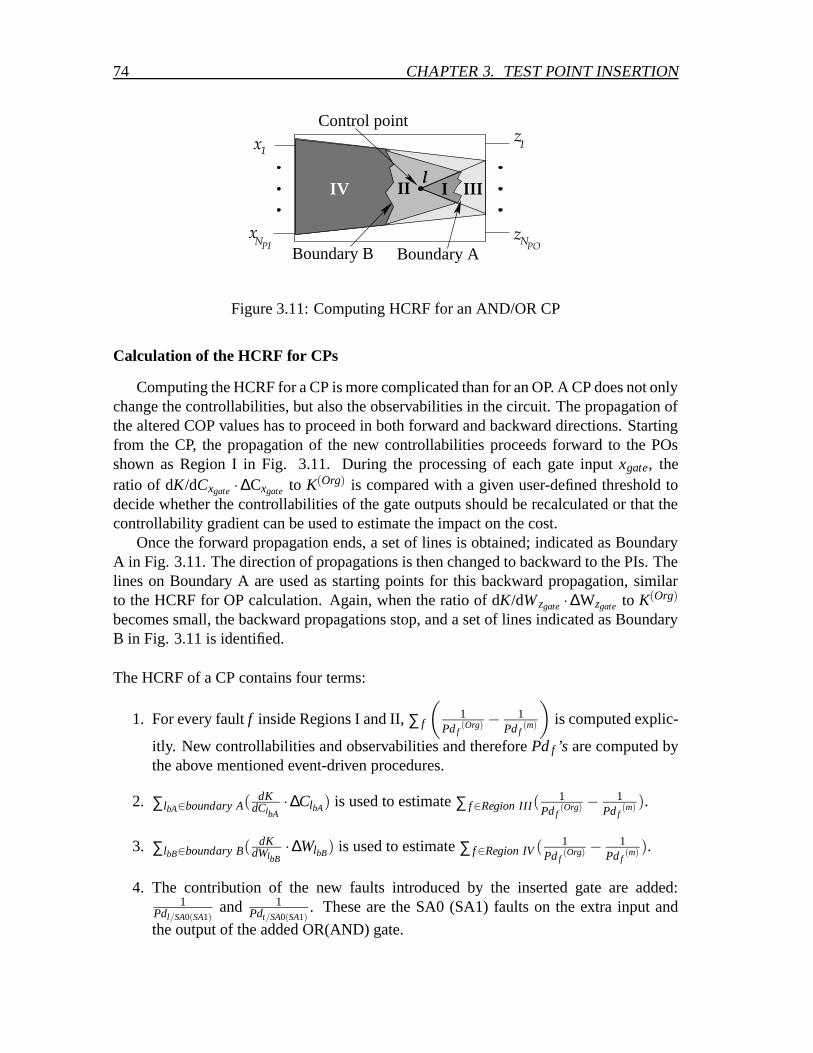
74 CHAPTER 3. TEST POINT INSERTION
II
z
x
x
zControl point
1
NPI NPO
1
l
Boundary B Boundary A
IIV III
Figure 3.11: Computing HCRF for an AND/OR CP
Calculation of the HCRF for CPs
Computing the HCRF for a CP is more complicated than for an OP. A CP does not onlychange the controllabilities, but also the observabilities in the circuit. The propagation ofthe altered COP values has to proceed in both forward and backward directions. Startingfrom the CP, the propagation of the new controllabilities proceeds forward to the POsshown as Region I in Fig. 3.11. During the processing of each gate input xgate, theratio of dK/dCxgate ·∆Cxgate to K(Org) is compared with a given user-defined threshold todecide whether the controllabilities of the gate outputs should be recalculated or that thecontrollability gradient can be used to estimate the impact on the cost.
Once the forward propagation ends, a set of lines is obtained; indicated as BoundaryA in Fig. 3.11. The direction of propagations is then changed to backward to the PIs. Thelines on Boundary A are used as starting points for this backward propagation, similarto the HCRF for OP calculation. Again, when the ratio of dK/dW zgate ·∆Wzgate to K(Org)
becomes small, the backward propagations stop, and a set of lines indicated as BoundaryB in Fig. 3.11 is identified.
The HCRF of a CP contains four terms:
1. For every fault f inside Regions I and II, ∑ f
(
1Pd f
(Org) −1
Pd f(m)
)
is computed explic-
itly. New controllabilities and observabilities and therefore Pd f ’s are computed bythe above mentioned event-driven procedures.
2. ∑lbA∈boundary A( dKdClbA
·∆ClbA) is used to estimate ∑ f∈Region III(1
Pd f(Org) −
1Pd f
(m) ).
3. ∑lbB∈boundary B( dKdWlbB
·∆WlbB) is used to estimate ∑ f∈Region IV ( 1Pd f
(Org) −1
Pd f(m) ).
4. The contribution of the new faults introduced by the inserted gate are added:1
Pdl/SA0(SA1)and 1
Pdt/SA0(SA1). These are the SA0 (SA1) faults on the extra input and
the output of the added OR(AND) gate.

3.7. STATE-OF-THE-ART TPI ALGORITHMS 75
The equations to compute the HCRF for OR-type and AND-type CPs become:
HCRFORl = ∑
f∈Regions I&II
(
1
Pd f(Org)
−1
Pd f(m)
)
− ∑lbA∈boundary A
(dK
dClbA
·∆ClbA
)
− ∑lbB∈boundary B
(dK
dWlbB
·∆WlbB
)
−
(
1Pdl/SA0
+1
Pdt/SA0
)
(3.29)
HCRFANDl = ∑
f∈Regions I&II
(
1
Pd f(Org)
−1
Pd f(m)
)
− ∑lbA∈boundary A
(dK
dClbA
·∆ClbA
)
− ∑lbB∈boundary B
(dK
dWlbB
·∆WlbB
)
−
(
1Pdl/SA1
+1
Pdt/SA1
)
(3.30)
Every line lbB on Boundary B can be viewed as a pseudo-OP such that the superpo-
sition ∑lbB( dK
dWlbB·∆WlbB) can be used to estimate ∑ f
(
1Pd f
(Org) −1
Pd f(m)
)
for faults in-
side Region IV. Similarly, every line lbA on Boundary A can be viewed as a pseudo-CP and ∑lbA
( dKdClbA
·∆ClbA) is used to estimate the contribution for faults inside Region
III. A CP however, affects the testabilities of both its fan-ins and fan-outs. Inserting aset of CPs on Boundary A should have effects on all faults in Regions I-IV. This means∑lbA∈boundary A( dK
dClbA·∆ClbA) also contains contributions from Region I, II and IV. Because
the contribution from Region III usually dominates dKdClbA
·∆ClbA , the error by this approx-
imation is negligible.Furthermore, unlike OPs which always reduce K when they are inserted simultane-
ously, the effects of CPs can cancel one another if they are added at the same time. For
these reasons, using ∑lbA∈boundary A( dKdClbA
·∆ClbA) to estimate ∑ f
(
1Pd f
(Org) −1
Pd f(m)
)
for
the faults f is just a heuristic.
The Hybrid CRF TPI Algorithm
The Hybrid CRF TPI Algorithm is listed in Algorithm 3.3. Instead of pre-selecting aset of TP candidates that is further analyzed by calculating their ACRFs, for all lines theHCRF for a CP and the HCRF for an OP are calculated. Given all L lines in the circuit,the line lCP with the highest HCRF for AND/OR CPs is selected. Also the line lOP withthe highest HCRF for OPs is selected. When the highest HCRF for CPs is larger than thehighest HCRF for OPs, a CP is inserted at line lCP, otherwise an OP is inserted at line lOP.
In the Hybrid CRF TPI algorithm it is assumed that for all lines in the circuit theHCRFs are calculated. There are of course lines in the circuit which can be excluded asTP candidate in advance. All inputs (PIs/POs and SFF in/outputs) can be excluded asTP candidate. When timing information is available, i.e., critical paths in the circuit areknown, also the lines at which a TP would result in a performance degradation, i.e., wouldincrease the critical path length, can be excluded as TP candidate.

76 CHAPTER 3. TEST POINT INSERTION
Algorithm 3.3 Hybrid CRF Test Point InsertionInput: CUT, desired cost (KKKdesired), TTT PPPmax
Output: CUT with TPs
while ( KKK > KKKdesired) and (#TTT PPPsss < #TTT PPPmax) dofor all lines lll ∈ CUT do
Evaluate controllability CCCl and observability WWW l
Compute the gradients dKKK/dWWW l and dKKK/dCCCl
Compute HHHCCCRRRFFFOPl
if (dKKK/dCCCl < 0) thenCompute HHHCCCRRRFFFOR
lelse
Compute HHHCCCRRRFFFANDl
Select line lllCP with ∀lll∈CUT(HHHCCCRRRFFFAND/ORl <= HHHCCCRRRFFFCPmax)
Select line lllOP with ∀lll∈CUT(HHHCCCRRRFFFOPl <= HHHCCCRRRFFFOPmax)
if (HHHCCCRRRFFFCPmax >= HHHCCCRRRFFFOPmax) thenif (dKKK/dCCClCP < 0) then
Insert an OR type CP at line lllCP
elseInsert an AND type CP at line lllCP
elseInsert an OP at line lllOP
Experimental results of the Hybrid TPI algorithm
Tables 3.4 and 3.5 show figures, taken from [Tsa97], representing the quality of theTPs selected by the Hybrid TPI algorithm, respectively the CRF TPI algorithm describedin Subsection 3.7.1. Twenty TPs are selected sequentially for the ISCAS’85 circuits c2670and c7552. At each iteration, the ACRFs for all possible TPs are computed explicitly andsorted in a descending order. Then the ranks of the TPs selected by the Hybrid TPI al-gorithm and by the CRF TPI algorithm are checked. The columns in Tables 3.4 and 3.5show the rank of the TPs selected by the HCRF, respectively CRF TPI algorithm, for eachiteration.
The results show that the TPs selected by the Hybrid TPI algorithm are almost iden-tical to the ones with the highest ACRFs. Except for the nineteenth iteration, the HCRFselects the TP with the highest ACRF for circuit c2670. At the nineteenth iteration itstill selects the second best. During the first nine iterations for circuit c7552, the HCRFselects the TP candidate with the highest ACRF, at the tenth iteration, the 7th best ACRFcandidate is chosen and between iterations 11 and 20 all TP candidates are in the top 3.
The rank of the TPs selected by the CRF TPI algorithm is sometimes quite off thehighest ranked ACRF candidate, especially for circuit c2670. Between the tenth andtwentieth iteration, the rank of the CRF TP is between 1991 and 1925 of approximately

3.7. STATE-OF-THE-ART TPI ALGORITHMS 77
Table 3.4: Rankings of TPs selected by the Hybrid TPI algorithm
IterationCircuit 1st 2nd 3rd 4th 5th 6th 7th 8th 9th 10th
c2670 1 1 1 1 1 1 1 1 1 1c7552 1 1 1 1 1 1 1 1 1 7
IterationCircuit 11th 12th 13th 14th 15th 16th 17th 18th 19th 20th
c2670 1 1 1 1 1 1 1 1 2 1c7552 1 1 1 2 2 1 3 2 1 1
Table 3.5: Rankings of TPs selected by the CRF TPI algorithm
IterationCircuit 1st 2nd 3rd 4th 5th 6th 7th 8th 9th 10th
c2670 106 8 4 6 1 3 1 1 1 1881c7552 1 1 11 1 1 1 1 1 1 29
IterationCircuit 11th 12th 13th 14th 15th 16th 17th 18th 19th 20th
c2670 1881 1885 1895 11 1901 1901 1911 1 1925 1925c7552 1 1 3 2 1 1 1 2 1 1
2670 TP candidates. The CRF TP ranks for circuit c7552 are not so far off and except foriterations three and ten, all ranks are in the top 3.
Whether the more accurate TP selection of the Hybrid TPI algorithm also results inhigher fault coverages is shown in Table 3.6. This table shows results taken from [Tsa97]of the Hybrid TPI algorithm and the CRF TPI algorithm on eight, RPR, ISCAS’85 andISCAS’89 benchmark circuits. The circuits have been first optimized for performanceusing Berkeley SIS synthesis system [Sen92] and are mapped into Lucent 0.9 micronCMOS cell library. In this experiment, the threshold of scheduling an event for propaga-tion or using the gradients to estimate the impact on the cost, is set to 0.1% for HCRFOBS,for HCRFOR and for HCRFAND. The fault coverages shown are computed after applying32,000 PR patterns. For both TPI algorithms, the same number of TPs are inserted, listedin Column #TP. The fault coverages and CPU times are shown in Columns FC(%) andCPU time for respectively the Hybrid TPI algorithm and the CRF TPI algorithm. ColumnCPU time ratio(%) shows the ratio of the CPU time of the Hybrid TPI algorithm to that ofthe CRF TPI algorithm. The CPU time is measured on a SUN SPARCstation 5.
The results show that indeed the Hybrid TPI algorithm results in the same (circuitsc2670, s3384) or higher fault coverages (the other six listed circuits) than the CRF TPI

78 CHAPTER 3. TEST POINT INSERTION
Table 3.6: Comparison between the Hybrid and the CRF TPI algorithm
Hybrid CRF CPU timeCircuit #TP FC(%) CPU time FC(%) CPU time ratio(%)c2670 5 98.31 78.0 sec. 98.31 264.0 sec. 30c7552 10 98.23 3.4 min. 97.92 22.0 min. 15s3330 13 99.92 4.9 min. 99.39 29.0 min. 17s3384 9 99.78 128.0 sec. 99.78 659.0 sec. 19s4863 2 99.64 61.0 sec. 99.61 201.0 sec. 30s9234 19 96.10 12.3 min 94.79 75.0 min. 16s15850 34 97.41 34.4 min. 97.08 7.7 hr. 7s38417 46 99.19 1.7 hr. 98.84 92.1 hr. 2
∑ 138 98.49 2.7 hr. 98.08 102.2 hr. 3
algorithm. The last line in Table 3.6 shows the average fault coverages achieved after TPIfor both algorithms. These averages are calculated taking into account the circuit size.The CRF TPI algorithm reaches an average of 98% fault coverage. 2% of all faults arenot covered by the 32,000 PR patterns. On average, the Hybrid TPI algorithm only misses1.5% of the faults and covers 98.5%.
The CPU time ratio figures show that the Hybrid TPI algorithm runs faster than theCRF TPI algorithm. Only 2% (for circuit s38417) up to 30% (for circuits c2670 ands4863) of the time that the CRF TPI algorithm takes, is spent by the Hybrid CRF algo-rithm. The last line shows the total time spent on TPI for both algorithms. The Hybrid TPIalgorithm only takes 3% of the time that the CRF TPI algorithm consumes. Especiallythe TPI runs on the two largest of the eight circuits (s15850, s38417) are much faster withthe Hybrid TPI algorithm and cause this large speed difference. These results show thatthe Hybrid TPI algorithm is more feasible on larger designs than the CRF TPI algorithm.This large reduction of the CPU time for the Hybrid TPI algorithm mainly comes from theelimination of the second step in the CRF TPI algorithm, the calculation of the ACRFs.
3.7.3 Multi-phase Test Point Insertion
The Multi-phase TPI (MTPI) algorithm [Tam96] is based on a constructive methodol-ogy. A divide and conquer technique is used to partition the entire PR test set into multiplephases. In each phase a group of TPs (both CPs and OPs), targeting a specific set of faults,is selected. Within a particular phase of the test, one group of CPs is enabled and the otherCPs are disabled. This remains the same during the whole phase, i.e., during a particu-lar phase the CPs are controlled by fixed values. On the other hand, the CPs selectedby the (H)CRF TPI algorithm are driven by independent, equi-probable signals insteadof fixed ones, and test application is performed in a single session by enabling all CPs

3.7. STATE-OF-THE-ART TPI ALGORITHMS 79
Faul
t cov
erag
e
0 1 2
100 %
Test length3
Figure 3.12: FC plot of a circuit which test is divided into 4 phases
(equi-probable) and OPs simultaneously. Because CPs can be enabled simultaneously,it is possible that they have conflicting values such that some faults remain undetected.With MTPI this can be avoided by enabling possible conflicting CPs in different phases.
An example of the division into phases is given in Fig. 3.12. As is shown, eachphase contributes to the results achieved so far, moving the solution closer to completefault coverage. The design of each phase, i.e., the selection of CPs and OPs, is guided byprogressively reducing the set of undetected faults. Within each phase, CPs are identifiedwhich maximally contribute to the fault coverage achieved so far. A probabilistic faultsimulation technique is used to compute the impact of a new CP in the presence of theCPs selected so far.
The MTPI BIST scheme and methodology
Fig. 3.13 illustrates the main components of the MTPI BIST scheme, which uses theSTUMPS approach.2 The BIST controller contains a Pattern counter and a Phase decoder .The phase decoder plays a key role in the MTPI BIST scheme. The pattern counter isused as input for the phase decoder to know in which phase the test is. The outputs of thephase decoder are used to enable the group of CPs belonging to the current phase.
In Fig. 3.13, the test T has been divided into four phases, e.g., φ0 . . .φ3. The corre-sponding phase decoder output values during the test are shown in Fig. 3.14. In the firstphase φ0, the first quarter of the test, all CPs are disabled: a′ = a and b′ = b. During phaseφ1 (φ1 = 1, φ2 = φ3 = 0), the AND-type CP CPa is enabled, forcing line a′ to 0, whilethe OR-type CP CPb is disabled; the value of line b′ equals the value b. During phase φ2
both CPs CPa and CPb are enabled, forcing line a′ to 0 and line b′ to 1. Finally, in phaseφ3 only CP CPb is enabled, line b′ is forced to 1 while the value of line a is propagatedunchanged to line a′.
2The scan-chains, including the surrounding scan-chains are still present in MTPI BIST, however notshown to keep Fig. 3.13 clear.

80 CHAPTER 3. TEST POINT INSERTION
b
1
3
2
POs
scan−chains outputs
scan−chains inputs
PIs
CircuitC
OR
Ecounter
BISTcontroller
a a’
b’
CPa
bCP
BISTwith
11
1&
Phase decoder
Pattern
PRTPG (LFSR/CA)
ORA (MISR)
Figure 3.13: MTPI BIST scheme
3/4T1/2T1/4T T
0
0
b
b
b’a’
0
0
a
aphas
e en
able
sig
nals
test patterns
0
1
2
3
0
1
2
3
Figure 3.14: Impact MTPI phase decoder outputs on CPs
The MTPI BIST scheme will be described using the MTPI algorithm listed in Algo-rithm 3.4. Given as inputs the CUT, the test length (number of PR patterns), the targetfault coverage, the maximum number of CPs and OPs (CPmax, OPmax), the number ofphases (Φ) and the minimum-benefit-per-cost (MBPC) parameter, the objective of the al-gorithm is to perform circuit modification such that the target fault coverage is met withinthe specified test length, while satisfying the constraints on the number of CPs/OPs, witha minimum number of phases. The MBPC value is a parameter which can be used to tunethe algorithm and will be described further on.
In each phase, a collection of CPs and OPs are inserted iteratively by assessing their

3.7. STATE-OF-THE-ART TPI ALGORITHMS 81
Algorithm 3.4 MTPI BISTInput: CUT, number of PR patterns (TTT ), Target fault coverage (FFFCCCtarget), CCCPPPmax,
OOOPPPmax, number of phases (ΦΦΦ), Minimum-benefit-per-cost (MMMBBBPPPCCC)Output: CUT with TPs that reaches FFFCCCtarget
Perform fault simulation on TTT patternsif (fault coverage >= FFFCCCtarget) then
exitfor Phase 0 to ΦΦΦ-1 do
Get the list of undetected faults
{ CPs selection }while (#CCCPPPsss < CCCPPPmax) do
Perform probabilistic fault simulationList the set of CP candidatesEvaluate the set of CP candidatesSelect the best OP candidate: CCCPPPbest
if (CCCPPPbest meets MMMBBBPPPCCC criterion) thenInsert CP CCCPPPbest
elsebreak
{ OPs selection }Perform probabilistic fault simulationwhile (#OOOPPPsss < OOOPPPmax) do
List the set of OP candidatesEvaluate the set of OP candidatesSelect the best OP candidate: OOOPPPbest
if (OOOPPPbest meets MMMBBBPPPCCC criterion) thenInsert OP OOOPPPbest
elsebreak
Perform fault simulation on TTT patternsif (fault coverage >= FFFCCCtarget) then
exit
impact on the fault coverage. The consequences of inserting a CP/OP at a circuit lineare determined by means of a technique called probabilistic fault simulation (PFS) . ThePFS technique [Tam96] computes detection probabilities for the set of undetected faultsat different lines in the circuit, using analytical methods. This information, along with thedetection threshold, is then used to guide the selection of TPs. The value of the detectionthreshold needs to be determined by considering factors like the phase duration (numberof patterns in a phase) and the desired detection confidence. This detection threshold can

82 CHAPTER 3. TEST POINT INSERTION
be varied across different phases.The design of a particular phase is concluded when it is determined that the expected
benefit of a CP/OP does not justify the associated cost of implementation. The user-defined threshold minimum-benefit-per-cost (MBPC) is used for this purpose. The finalstep is to fault simulate the phase so that the list of undetected faults required for thedesign of a subsequent phase is determined.
OP Selection
The purpose of this step is to identify a pre-specified number of lines that enable thedetection of a maximum number of faults. The objective is to select the lines such thatthe detection probability of a maximum number of faults meets a user specified thresholdDTh. A three steps process is followed to achieve this objective.
First, probabilistic fault simulation is performed to determine the propagation profile.This information is represented as a sparse matrix TML×F , with the L collected lines asrows, the F undetected faults as columns, and the probability of detecting a fault f on linel as entry TMl, f . In order to reduce the memory requirements, faults that propagate to aline with a probability less than a certain minimum threshold are dropped. In addition,lines that carry less than a minimum number of faults, as determined by the minimum-benefit-per-cost (MBPC (see Algorithm 3.4) criterion, are eliminated. The problem ofselecting a pre-specified number of OPs, becomes equivalent to that of selecting the set ofrows which maximizes the number of columns satisfying the detection probability DTh.This is an NP-complete problem, for which [Tam96] shows a greedy heuristic selectionmethod to solve it.
CP Selection
The RPR problem cannot be entirely solved by inserting OPs alone, CPs are needed aswell. In the MTPI scheme, CPs are driven by fixed values and are aimed at improving theexcitation probability and propagation of specific faults. The insertion of CPs is dividedinto three steps:
1. Probabilistic fault simulation is performed to determine the propagation profile.
2. The set of candidate positions for CP insertion is determined.
3. The best CP candidate is selected, by determining the benefit of each candidatethrough incremental probabilistic fault simulation.
These steps are explained below:
The CP selection aims at quickly identifying the set of CP candidate lines. It is neces-sary to eliminate ineffective lines early on so that time spent in the subsequent selectionstep is reduced. However, good candidates must not be missed; they are determined by an

3.7. STATE-OF-THE-ART TPI ALGORITHMS 83
estimation technique that computes two estimates, E0 and E1 for various lines in the cir-cuit. These measures give an indication of the number of faults that could potentially bedetected by placing an AND/OR-type CP respectively. Lines for which E0 or E1 exceedsa minimum acceptable value are retained for subsequent evaluation.
The computation of E0 and E1 utilizes the propagation profile information and isdriven by three pre-specified parameters:
1. Minimum Probability Threshold MPTh which specifies the minimum acceptablevalue for 0(1) probability at a line in the circuit.
2. Low Threshold LTh
3. High Threshold HTh
A line for which the 0-probability(1-probability) falls below MPTh is called a 0-failing (1-failing) line. For each 0-failing (1-failing) line in the circuit, a constant 0-value (1-value)is injected at that line and the consequent signal probability changes are determined. Thevalues LTh and HTh are used to record changes in signal probability of lines due to theinsertion of a CP. A line for which the 0 or 1 probability changes from a value below LThto a value above HTh after the insertion of a CP is said to facilitate the excitation andpropagation of certain faults. For the purpose of estimation, such faults are consideredto be detected. Hence, the estimation procedure predicts the number of faults that couldbe detected by a CP by reasoning about the impact of signal probability changes on thefaults.
Starting from the CP candidate location, the probability changes are computed in alevelized, selective-trace manner. For each gate that is affected, new signal probabili-ties are obtained. Fan-outs of the affected gate are scheduled for evaluation only if thenew signal probabilities deviate from the original signal probabilities by more than a pre-specified threshold. The signal probability changes, along with the threshold LTh andHTh, are then used to compute the estimates E0 and E1.
The rank of each CP candidate is defined as the number of additional faults that propa-gate to POs or OPs. The candidate with the highest rank is then selected for CP insertion.
Experimental results of the MTPI algorithm
Table 3.7 shows experimental results [Tam96], of the MTPI algorithm on the IS-CAS’85 benchmark circuits c2670 and c7552 and five ISCAS’89 benchmark circuits.For each circuit first the redundant faults have been eliminated. The objective of theexperiment is to achieve (near) complete fault coverage with 32,000 PR patterns, and aminimum of phases.
Before the TPI algorithm is run, the number of phases (Φ), the duration and thenumber of CPs and OPs, have to be determined. Φ is chosen to be an arbitrary value, andthe entire test length among these phases is evenly distributed. Fault simulation for phaseφ0 is then performed using a fast fault simulator. The set of undetected faults is used to
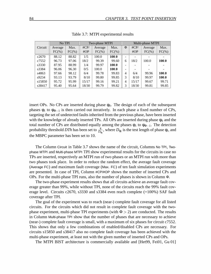
84 CHAPTER 3. TEST POINT INSERTION
Table 3.7: MTPI experimental results
No TPI Two-phase MTPI Multi-phase MTPICircuit Average Max. #CP/ Average Max. Φ #CP/ Average Max.
FC(%) FC(%) #OP FC(%) FC(%) #OP FC(%) FC(%)
c2670 88.12 88.82 1/5 100.0 100.0 - - - -c7552 96.73 97.06 18/2 99.39 99.60 6 18/2 100.0 100.0s3330 87.95 88.99 1/4 99.97 100.0 - - - -s3384 96.06 96.30 0/5 100.0 100.0 - - - -s4863 97.66 98.12 6/4 99.78 99.83 4 6/4 99.96 100.0s9234 93.13 93.79 8/10 99.80 99.85 3 8/10 99.97 100.0s15850 95.72 95.99 15/17 99.16 99.21 4 15/17 99.67 99.71s38417 95.40 95.64 18/30 99.79 99.82 3 18/30 99.81 99.85
insert OPs. No CPs are inserted during phase φ0. The design of each of the subsequentphases φ1 to φΦ−1 is then carried out iteratively. In each phase a fixed number of CPs,targeting the set of undetected faults inherited from the previous phase, have been insertedwith the knowledge of already inserted TPs. All OPs are inserted during phase φ0 and thetotal number of CPs are distributed equally among the phases φ1 to φΦ−1. The detectionprobability threshold DTh has been set to 4
Dφi, where Dφi is the test length of phase φi, and
the MBPC parameter has been set to 10.
The Column Circuit in Table 3.7 shows the name of the circuit, Columns No TPI, Two-
phase MTPI and Multi-phase MTPI TPI show experimental results for the circuits in case noTPs are inserted, respectively an MTPI run of two phases or an MTPI run with more thantwo phases took place. In order to reduce the random effect, the average fault coverage(Average FC) and maximum fault coverage (Max. FC) of ten fault simulation experimentsare presented. In case of TPI, Column #CP/#OP shows the number of inserted CPs andOPs. For the multi-phase TPI runs, also the number of phases is shown in Column Φ.
The two-phase experiment results shows that all circuits achieve an average fault cov-erage greater than 99%, while without TPI, none of the circuits reach the 99% fault cov-erage level. Circuits c2670, s3330 and s3384 even reach complete (=100%) SAF faultcoverage after TPI.
The goal of the experiment was to reach (near-) complete fault coverage for all listedcircuits. For the circuits which did not result in complete fault coverage with the two-phase experiment, multi-phase TPI experiments (with Φ > 2) are conducted. The resultsin Column Multi-phase TPI show that the number of phases that are necessary to achieve(near-) complete fault coverage is small, with a maximum of six phases for circuit c7552.This shows that only a few combinations of enabled/disabled CPs are necessary. Forcircuits s15850 and s38417 also no complete fault coverage has been achieved with themulti-phase experiment, at least not with the given number of inserted CPs and OPs.
The MTPI BIST architecture is commercially available and [Het99, Fei01, Gu 01]

3.7. STATE-OF-THE-ART TPI ALGORITHMS 85
networkp
inout
Vdd
Vss
X
X
networkn
i
i
(a) A 1-controllable gate
networkn
networkp
out
Vdd
Vss
in
X
Xi
i
(b) A 0-controllable gate
Figure 3.15: AND/OR TP alternatives
provide case studies of the MTPI algorithm on industrial designs. They show that MTPIBIST is applicable to industrial circuits as long as the circuits are BIST & TPI ready, orcan be made BIST & TPI ready, i.e., meet the requirements for BIST & TPI implementa-tion as given in Sections 2.3 and 3.4.
3.7.4 Other state-of-the-art TPI algorithm
In Schotten et al. [Sch95], a TPI algorithm is presented for an area efficient BIST. Likethe adjusted CRF TPI algorithm presented in [Che95b], the TPI algorithm in [Sch95] doesnot require a full-scan circuit. Like the (H)CRF TPI algorithms, [Sch95] uses controllabil-ities, observabilities and a cost function to determine the best TP positions in the circuit,although different controllability, observability and cost equations are used than the COPequation on which the (H)CRF TPI algorithms are based. [Sch95] claims that their algo-rithm is inefficient in case of large circuits with poor controllability, therefore we have notlooked further into this method.
In [Tou96] a test set dependent TPI method is presented, which is based on path trac-ing. Fault simulation is used to identify faults that are not detected by a given set of testpatterns, e.g., a set of ATPG patterns. For each undetected fault, a path tracing procedureis used to identify the set of TPs that will enable the fault to be detected. This set is theset of TP solutions for the fault. Given the set of TP solutions for each undetected fault,a minimal set of TP is selected to achieve the desired fault-coverage, using a set cover-ing procedure. The set covering procedure is an NP-complete problem. Although goodheuristics exist [Chr75], this can result in very large CPU times for larger circuits withmany undetected faults.
In [Sav91] and [You93] alternatives for AND/OR TPs are presented. Instead of ANDand OR gate, the solution given in Fig. 3.15 is used. This is called the Force-Observe

86 CHAPTER 3. TEST POINT INSERTION
(F-O) approach. When the Xi input of Fig. 3.15(a) is set to 0, the output (OUT) is forcedto 1. Similarly, when the Xi input in Fig. 3.15(b) is set to 1, the output is forced to 0.Thus, when a value of a node is needed to control to one, the gate driving it is replaced bythe controllable element of Fig. 3.15(a). If a node has to be controlled to zero, the gatedriving it is replaced by the element of Fig. 3.15(b). Simulations [You93] have shownthat the speed degradations observed with the F-O approach are generally smaller thanthose introduced by the classical AND/OR TPs. The F-O TPs are useful to achieve agood controllability at the cost of a minimal speed degradation. With highly loaded nodeshowever, classical AND/OR TPs offer a better performance and they should preferablybe used.
3.8 Overview TPI topics in this dissertation
Subsection 3.8.1 provides an overview of the TPI topics that are addressed in theremaining part of the dissertation. In order to test and compare the TPI algorithms andtechniques that are proposed in the following chapters, several TPI benchmark circuitshave been used. These circuits are described in Subsection 3.8.2
3.8.1 TPI topics overview
In the following three chapters, the application of TPI on improving BIST fault cov-erage, respectively on facilitating stuck-at fault ATPG, and on facilitating gate-delay faultATPG, are addressed. In all cases, the HCRF TPI algorithm is used as a base for furtherdevelopment, as will be explained in Chapter 4. COP, that is used in the CRF and HCRFTPI algorithms, can only cope with Boolean values. Therefore COP will be extended inChapter 4 such that the HCRF TPI algorithm becomes applicable to industrial circuits,i.e., circuits containing three-state elements and unknown values. In Chapter 4 a newcost function will be proposed with which better PR fault coverage improvements can beachieved. Also a technique is proposed that reduces the number of TP candidates in thecircuit, without impacting the quality of the TP selection.
In Chapter 5 it will be shown that the HCRF TPI algorithm is not only able to improveBIST fault coverages, but is also able to reduce stuck-at fault test set sized generated bya compact ATPG tool. The HCRF TPI algorithm is not aimed on reducing the compactATPG test set sizes. Therefore, in Chapter 5, new cost functions and techniques are intro-duced that are aimed on reducing stuck-at fault ATPG test set sizes, such that better testset size reductions can be achieved.
In Chapter 6 it will be shown what the impact is of TPI for stuck-at fault ATPG on theATPG test set sizes for gate-delay faults. It will be shown that TPI significantly reducesgate-delay fault test set sizes as well.

3.8. OVERVIEW TPI TOPICS IN THIS DISSERTATION 87
3.8.2 TPI benchmark circuits
In order to evaluate the various TPI methods and techniques, several TPI benchmarkcircuits have been used in this dissertation. These benchmark circuits consist of circuitsthat are commonly used in literature for benchmarking test related algorithms, i.e., theISCAS circuits [Brg85, Brg89, Kis89] and circuit (cores) that were actually used in com-mercial industrial products.
The properties of the ISCAS benchmark circuits used throughout this dissertation aredescribed in Appendix A and consist of the following three groups of circuits:
1. ISCAS’85Eight of the ISCAS’85 benchmark circuits [Brg85] have been used in this disserta-tion for benchmarking TPI, i.e., circuits c880, c1355, c1908, c2670, c3540, c5315,c6288 and c7552. These ISCAS’85 circuits are all Boolean combinational logiccircuits not containing any memory elements. The number in the name gives anindication of the number of signal lines in the circuit.
2. ISCAS’89In 1989 a new set of ISCAS benchmark circuits has been introduced by Brglez[Brg89] that consists of Boolean sequential circuits, circuits containing memoryelements, i.e., flipflops. Eleven of these circuits have been benchmarked through-out this dissertation, i.e., circuits s1196, s1423, s1488, s1492, s5378, s9234.1,s13207.1, s15850.1, s35932, s38417 and s38584.1.
3. ISCAS’89aAlso in 1989 a set of addendum circuits [Kis89] has been added to the original setof ISCAS’89 circuits. Ten of these ISCAS’89 addendum circuits have been used forbenchmarking, i.e., circuits s499a, s635a, s938a, s1269a, s1512a, s3271a, s3330a,s3384a, s4863a and s6669a.
The industrial designs used for benchmarking TPI are all Philips industrial circuits. Prop-erties of these industrial circuits are found in Appendix B. These industrial benchmarkcircuits consist of the following groups of circuits:
1. Philips Boolean designsFifteen Boolean Philips designs have been used for benchmarking TPI, i.e., cir-cuits p5973, p7653, p13138, p14148, p27811, p31025, p34592, p36503, p43282,p43663, p72767, p73133, p73257, p75344 and p162057. Like for the ISCAS cir-cuits, the number in the name is an indication of the number of signal lines in thecircuit. All of these listed circuits are cores/parts of commercial industrial ICs. Al-though being industrial designs, these circuits do not contain three-state elements.Only circuit p162057 contains fixed unknown inputs.
2. Philips three-state designsBesides Boolean circuits, also fourteen industrial designs containing three-state
88 CHAPTER 3. TEST POINT INSERTION
elements and/or fixed unknown inputs are used for benchmarking, i.e., circuitsp32118, p37021, p66171, p71553, p93140, p104649, p114605, p137498, p481470,p596922, p598004, p705050, p824184 and p854266. Circuits p71553 and p93140are designed only for test purposes, the remaining circuits are parts of commercialdesigns.
3.9 Summary and conclusions
The purpose of test point insertion (TPI) is to insert extra logic, i.e., test points (TPs),into the circuit to improve the testability of the circuit. TPs consist of control points (CPs)and observation points (OPs). CPs are inserted to improve the controllability of lines andOPs to improve the observability of lines. Traditionally, CPs consist of an extra inputconnected to an extra inserted AND/OR gate at a line in the circuit. With the extra in-put, the output of the AND(OR) gate can be forced to 0(1), bypassing the logic in thefan-in cone of the line where the CP is inserted. OPs consist of extra inserted outputs. Inscan-designs, CPs and OPs are often controlled and observed by extra SFFs. These SFFsthemselves can also be used as TPs, at least when they are transparent during normal ap-plication mode.
TPI can be used to facilitate testing in different ways, e.g., it can be used to improvePR fault coverage or to facilitate the generation of ATPG patterns. TPI algorithms can becategorized, depending on the method they use to determine the faults which testabilityshould be improved, into: ATPG, fault simulation, and testability analysis based methods.TPI methods can also be divided into methods that do take into account the test set thatwill be applied to the circuit, i.e., test set dependent methods, and TPI methods that donot take this information in account, i.e., test set independent methods.
In case of industrial circuits, TPI algorithms should be able to cope with three-statecircuits and avoid bus-conflicts. Also TPs at the critical paths should be avoided to pre-vent performance loss.
Several TPI algorithms, e.g.,the CRF TPI algorithm [Sei91], the Hybrid CRF (HCRF)TPI algorithm [Tsa97] and the Multi-phase TPI (MTPI) algorithm [Tam96] have been de-scribed which improve the fault coverages. Both the CRF and HCRF TPI algorithm use acost function, based on COP testability analysis measures, to select the best positions inthe circuit to insert TPs. Therefore first descriptions of COP, the cost function and costgradients have been given. Because most TPI algorithms for BIST assume a STUMPSarchitecture, also a description of the STUMPS architecture has been given.
Several sets of circuits have been described, i.e., ISCAS and Philips benchmark cir-cuits, that are used in this dissertation to benchmark TPI. In the following three chaptersTPI methods are described to facilitate BIST, facilitate ATPG, respectively facilitate gate-delay fault ATPG.

CHAPTER 4
Test Point Insertion for BIST
Section 4.1 starts with a comparison of the CRF, HCRF and MTPI algorithms de-scribed in Chapter 3 and summarizes their advantages and disadvantages. Also will beexplained why the HCRF TPI algorithm is chosen as a base for further TPI development.Section 4.2 describes how COP can be extended such that it is also applicable to industrialcircuits. Section 4.3 describes our proposed TPI algorithm for BIST. It includes experi-mental results that show that our proposed TPI algorithm results in significant PR faultcoverage improvement and is applicable to complex large industrial circuits containingthree-state elements. Also included in this section is a technique to speed-up the TPI al-gorithm without impacting the quality of TPI. Section 4.4 summarizes and concludes thischapter.
4.1 Comparison of the CRF, HCRF and MTPI algorithm
This section starts with comparing experimental results of the CRF, HCRF and MTPIalgorithms for BIST in Subsection 4.1.1, followed by a summary and conclusions in Sub-section 4.1.2. One of the main drawbacks of most TPI algorithms is that they do notsupport industrial circuits, i.e., circuits that contain lines that can become Z or U. Theimplications of industrial circuits on TPI and BIST are described in Subsection 4.1.3.
4.1.1 Comparison of the TPI experimental results
Table 4.1, taken from [Tsa97], shows a comparison of the TPI algorithms described inSection 3.7. The circuits, listed in Column Circuit have first been optimized by removingredundant faults from the fault list. Experimental results are shown for the CRF algo-rithm, respectively Hybrid CRF algorithm and MTPI algorithm. For the Hybrid CRF andMTPI algorithms, the number of CPs and number of OPs (Column #CP/#WP) are listed.No detailed information of the number of CPs and OPs is given for the CRF algorithm,therefore only the number of inserted TPs (Column #TP) is listed. The fault coverages
89
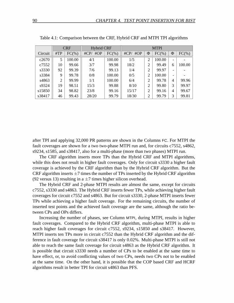
90 CHAPTER 4. TEST POINT INSERTION FOR BIST
Table 4.1: Comparison between the CRF, Hybrid CRF and MTPI TPI algorithms
CRF Hybrid CRF MTPICircuit #TP FC(%) #CP/ #OP FC(%) #CP/ #OP Φ FC(%) Φ FC(%)
c2670 5 100.00 4/1 100.00 1/5 2 100.00 - -c7552 10 99.66 3/7 99.98 18/2 2 99.49 6 100.00s3330 92 99.39 7/6 99.13 1/4 2 99.97 - -s3384 9 99.78 0/8 100.00 0/5 2 100.00 - -s4863 2 99.99 1/1 100.00 6/4 2 99.78 4 99.96s9324 19 98.51 15/3 99.88 8/10 2 99.80 3 99.97
s15850 34 98.82 23/8 99.16 15/17 2 99.16 4 99.67s38417 46 99.43 28/20 99.79 18/30 2 99.79 3 99.81
after TPI and applying 32,000 PR patterns are shown in the Columns FC. For MTPI thefault coverages are shown for a two two-phase MTPI run and, for circuits c7552, s4862,s9234, s1585, and s38417, also for a multi-phase (more than two phases) MTPI run.
The CRF algorithm inserts more TPs than the Hybrid CRF and MTPI algorithms,while this does not result in higher fault coverages. Only for circuit s3330 a higher faultcoverage is achieved by the CRF algorithm than by the Hybrid CRF algorithm. But theCRF algorithm inserts ±7 times the number of TPs inserted by the Hybrid CRF algorithm(92 versus 13) resulting in a ±7 times higher silicon overhead.
The Hybrid CRF and 2-phase MTPI results are almost the same, except for circuitsc7552, s3330 and s4863. The Hybrid CRF inserts fewer TPs, while achieving higher faultcoverages for circuit c7552 and s4863. But for circuit s3330, 2-phase MTPI inserts fewerTPs while achieving a higher fault coverage. For the remaining circuits, the number ofinserted test points and the achieved fault coverage are the same, although the ratio be-tween CPs and OPs differs.
Increasing the number of phases, see Column MTPI, during MTPI, results in higherfault coverages. Compared to the Hybrid CRF algorithm, multi-phase MTPI is able toreach higher fault coverages for circuit c7552, s9234, s15850 and s38417. However,MTPI inserts ten TPs more in circuit c7552 than the Hybrid CRF algorithm and the dif-ference in fault coverage for circuit s38417 is only 0.02%. Multi-phase MTPI is still notable to reach the same fault coverage for circuit s4863 as the Hybrid CRF algorithm. Itis possible that circuit s3330 needs a number of CPs to be enabled at the same time tohave effect, or, to avoid conflicting values of two CPs, needs two CPs not to be enabledat the same time. On the other hand, it is possible that the COP based CRF and HCRFalgorithms result in better TPI for circuit s4863 than PFS.

4.1. COMPARISON OF THE CRF, HCRF AND MTPI ALGORITHM 91
4.1.2 Summary of the CRF, HCRF and MTPI algorithms
CRF TPI: For each possible TP position in the CUT, the Cost Reduction Factor (CRF)is calculated. The CRF is an estimate for the cost reduction achieved by the TPand is calculated using local testability analysis (TA) information of a signal line,namely the COP controllability, observability and gradient values, no TA measuresof surrounding lines are taken into account. The gradients of a line reflect the impactof a controllability/observability change on that line on the entire circuit. The CRFsare not accurate enough for selecting a good TP position. For this reason, a set ofTP candidates is selected for which the Actual Cost Reduction Factor (ACRF) iscalculated. The ACRF is calculated by temporarily inserting the TP candidate inthe CUT, recalculating the cost and taking the difference between the original costand the cost after TPI. The TP that results in the largest ACRF will be implemented.
Advantage: The computation of the CRFs and gradient values are linear with thenumber of faults. They can be calculated fast.
Disadvantage: The CRFs are not accurate enough for TPI and calculating theACRF for every TP candidate is too time-consuming. The ACRF is only cal-culated for a limited set of TP candidates; it is possible that good TPs areexcluded because they are not included in the limited set of TP candidates.
Hybrid TPI: The Hybrid CRF algorithm uses the Hybrid Cost Reduction Factor (HCRF)as estimate for the ACRF. The HCRF is calculated by explicitly calculating thechanges in detectability probabilities of a line when the changes in controllabilityor observability are too large, and using the gradients when the changes are small.The calculation of the HCRF happens in an event-driven procedure. Starting fromthe TP, the observability and controllability changes are propagated toward PIs andPOs until the impact of the changes on the cost becomes below a given threshold.The HCRF values are more accurate than the CRFs and no ACRF calculation isneeded to find a good TP position.
Advantage: The HCRFs are more accurate than the CRFs. All TP candidates aretaken into account.
Disadvantage: Calculating an HCRF is slightly more time-consuming comparedto the CRF. However, the CRF algorithm requires ACRF calculation which isnot required for HCRFs. This algorithm is still based on TA estimates and doesnot take into account special information on the test set that will be applied tothe circuit during test.
Multi-phase TPI: The COP based algorithms enable their CPs independently and equi-probably during the entire test. In the Multi-phase TPI (MTPI) algorithm, duringany phase only one set of CPs is enabled and the other CPs are not. During thenext phase, another set of CPs is enabled. The same CPs can be in multiple setsand so be enabled during multiple phases. This algorithm first uses fault simulation
92 CHAPTER 4. TEST POINT INSERTION FOR BIST
to find the controllabilities of all lines and to get a list of undetected faults. Prob-abilistic Fault Simulation (PFS) is used to determine the propagation profile of thefaults. Estimates are used which reflect the number of undetected faults that will bedetected by inserting a TP. These estimates are calculated with the data found withPFS. TPs which lead to the largest number of faults to become detected during aphase, are selected.
Advantage: CPs that have a conflict when they are enabled at the same time canbe put in different phases such that they will never by enabled simultaneously.The results of (P)FS are more accurate than those of COP, because (P)FS takesadvantage of the test set that is used during test.
Disadvantage: This algorithm is much slower compared to the COP algorithms,because fault simulation and PFS are both more CPU time-consuming thanthe controllability/observability and cost calculations of COP. The lack of ran-domness in enabling CPs sometimes has a negative impact on the fault cover-age.
The CRF/Hybrid CRF algorithms are based on TA. This is faster and easier than us-ing (probabilistic) fault simulation as MTPI does. TA does not only give estimates forthe controllability and observability, but it also introduces a way to estimate the impactof a TP on the CUT. Fault simulation can result in better estimates for controllability andobservability, because the information of the test set used for testing can be taken intoaccount, but how to estimate the impact of a TP on the CUT is harder.
The Hybrid CRF algorithm outperforms the CRF algorithm; it is faster (taking intoaccount that for the CRF, also the ACRF values have to be calculated) and does resultin higher fault coverages. The MTPI and Hybrid CRF algorithm have comparable re-sults. The structure of a CUT has a large influence on determining which TPI algorithmis better. There are circuits for which conflicting CPs results in reduced fault coverageimprovement; these circuits benefit from the MTPI approach. For other circuits, the equi-probable CP enabling method used in the Hybrid CRF TPI algorithm outperforms thefixed enabling method used in the MTPI algorithm.
Case studies presented in [Het99, Fei01, Gu 01] have shown that the MTPI algorithmis also applicable to industrial designs. However, the MTPI TPI algorithm should be usedin combination with the multi-phase BIST scheme depicted in Figure 3.13; it cannot beused in combination with other BIST models. As the MTPI algorithm is integrated in theMTPI BIST scheme, it is not applicable for other purposes than BIST, e.g., it is not appli-cable to facilitate ATPG. The CRF and HCRF TPI algorithms are not integrated in a BISTmodel and therefore are not limited to a single BIST model, or even to BIST. They canalso be used to facilitate ATPG as will be shown in the following chapters. On the otherhand, they assume to be applied to Boolean circuits only. They do not take into accountany implications with respect to industrial circuits. The following subsection shows the

4.1. COMPARISON OF THE CRF, HCRF AND MTPI ALGORITHM 93
problems that a TPI algorithm for BIST has to solve in order to be able to be applied toindustrial circuits.
Because the HCRF TPI algorithm outperforms the CRF TPI algorithm, and the MTPIalgorithm is only applicable to one single BIST scheme, i.e., the MTPI BIST scheme, theHCRF TPI algorithm is chosen as a base for further TPI development. The Hybrid CRFTPI algorithm is fast; the results given in Subsections 3.7.2 and 4.1.1, show that it canresult in high fault coverages with only a few TPs; it is not very complex to implement,and because it is based on COP, it can be extended for industrial circuits as will be shownin the following sections. Although the COP controllability and observability estimatesare not too accurate themselves, the event-driven mechanism of propagating the changesfrom the TP candidate, results in fast and good TP selection (see Tables 3.4 and 3.6). Thisevent-driven mechanism can be seen as a basic method of determining the impact of TPcandidates on a circuit. Even with TA measures other than COP, this event-driven mech-anism with CFs is very useful as will be shown further on in this thesis. The algorithm isnot limited to be used only for improving PR fault coverage in a BIST environment. Forthis reason, The Hybrid CRF algorithm is chosen as base for a new proposed TPI algo-rithm for industrial circuits, which can cope with large and complex industrial, includingthree-state elements.
4.1.3 Implications of Z and U values on TPI and BIST
Besides 0 and 1 values, also Z and U values occur in industrial designs. Floatingvalues and unknown values can occur in case the circuit contains three-state elements,e.g., buses, switches, etc., or unknown fixed inputs, e.g., inputs from embedded memo-ries. These Z and U values impact the TPI process as this does have an impact on thecalculation of the COP TA measures and on PFS. Eq. 3.1 does not hold for lines that alsohave a probability on floating or unknown values. As a result, the COP equations givenin Table 3.1 are not applicable to circuits that can contain these values. These circuitsrequire extended COP equations which take into account probabilities on Z and U values.The same applies to PFS, also PFS has to take into account the probabilities on Z and Uvalues in the circuit.
Another problem of TPI for BIST in industrial circuits, is the handling of buses. Asdescribed in Section 2.3, conflicting buses should be avoided during a BIST test run. Be-sides damaging the CUT, conflicting buses cause unknown values that could be capturedby the MISR, making the complete MISR state unknown such that it cannot be checkedwhether the state of the MISR complies to a fault-free circuit. Inserting a TP nearby abus, might enable a bus to come in a conflicting state during PR BIST. This is depicted inFig. 4.1. The line select in Fig. 4.1(a) enables switch SWa or switch SWb (when Xd = 0)but never at the same time. However, due to the TP inserted before the control input of

94 CHAPTER 4. TEST POINT INSERTION FOR BIST
1
z
x
select
SWa
SWb
a
xd
xb
(a) Circuit with non-conflicting bus
1
& z
x
select
SWa
SWb
a
CP
xd
xcp
xb
(b) After TPI, a bus-conflict can occur
Figure 4.1: TPI on a circuit with buses can result in bus-conflicts
switch SWb, a bus-conflict occurs when lines a and b drive opposite values, select = 1,xd = 0 and xcp = 0. When a TPI algorithm is used for facilitating ATPG, see Chapter 5,this possibility of a bus-conflict is not a problem. The ATPG algorithm has to avoid thatthe combination select = 1, xd = 0 and xcp = 0 occurs, which should not be a problem.However, in a PR BIST environment, it is not known in advance what the values will befor these signal lines, the combination select = 1, xd = 0 and xcp = 0 is possible, resultingin the nasty bus-conflict. Therefore a TPI for BIST algorithm should make sure that noTPs are inserted in lines that might result in extra bus-conflicts during PR test.
The TPI algorithm proposed in Section 4.3 is be able to cope with industrial circuits.
4.2 COP for industrial circuits
In order to be able to use COP, or the COP based HCRF TPI algorithm, with cir-cuits that can contain Z or U values, we have extended COP to support probabilities onZ and U values. Subsection 4.2.1 shows how COP is extended with Z-controllability andU-controllability in order to deal with industrial circuits. Subsection 4.2.2 shows newobservabilities for industrial circuits and Subsection 4.2.3 shows the COP detection prob-ability equations for industrial circuits. The implications of the new COP TA measuresfor industrial circuits on the cost gradients are described in Subsection 4.2.4.
4.2.1 COP controllabilities in industrial circuits
In industrial circuits there are lines which do not only have a probability on being 0 or1, but also on floating (Z) or being unknown (U). Therefore Eq. 3.1 does not hold for these

4.2. COP FOR INDUSTRIAL CIRCUITS 95
circuits because it does not take into account these probabilities. Still the probabilities onall possible values for a signal line in an industrial circuit should add up to 1. Giventhis, Eq. 3.1 can been adjusted to Eq. 4.1, which does take into account float/unknownprobabilities.
C0l +C1l +CZl +CUl = 1
C0l = 1−C1l −CZl −CUl (4.1)
In Eq. 4.1, CZl is the COP probability on floating for line l and CUl is the COP probabilityon an unknown value. The controllability equations listed in Table 3.1 are based on Eq.3.1 and are therefore not valid for industrial circuits. Still, the output of an OR gate is only0 when all the input values are 0, hence the 0-controllability of OR gate output z (C0z),can be found by multiplying the 0-controllabilities of all inputs (C0xi). In case of Booleancircuits, if the output is not 0, it is 1 and C1z of the OR gate is found by 1−C0z. Thisis not valid in industrial circuits. However, it is still true that the output of an OR gate isonly not 1 when none of the X inputs of the OR gate are 1. Hence C1z of the output of theOR gate is 1 minus the probability that none of the inputs are 1. The probability that aninput xi is not 1, is 1−C1xi . Now C1z can be calculated with Eq. 4.2.
C1z = 1−X
∏i=1
(1−C1xi) (4.2)
The COP controllability equations of the other Boolean elements have been found in asimilar way and are listed in Appendix C.
The outputs of Boolean gates cannot be at high impedance, therefore the Z-controllabilityof an output z (CZz) of a Boolean gate is always 0. Outputs of Boolean gates can be un-known if there are inputs with unknown or floating values, therefore CUz of a Booleangate can be non-zero. Because CZz = 0 for Boolean gates, CZ can be determined with Eq.4.3.
CUz = 1−C1z −C0z (4.3)
The controllabilities for the three-state elements can be determined in a similar wayas for the Boolean elements. A three-state bus results in a 0 when one or more inputsare 0 and the remaining inputs are floating (Z). The probability that an input xi is 0 orZ is found with C0xi +CZxi . The probability that all lines are 0 or Z can be found bymultiplying (C0xi +CZxi) over all inputs. However, the bus only results in a 0, when atleast one input is 0, therefore the probability that all inputs are Z should be excluded,hence the equation for calculating C0z for a three-state bus becomes:
C0z =X
∏i=1
(C0xi +CZxi)−X
∏i=1
(CZxi) (4.4)
C1z of the three-state bus is found in the same way and is given by:
C1z =X
∏i=1
(C1xi +CZxi)−X
∏i=1
(CZxi) (4.5)

96 CHAPTER 4. TEST POINT INSERTION FOR BIST
PO1
data
Z
0
z1/0
Z/0
SA0
Figure 4.2: A Z↔0 discrepancy leading to a 0↔1 discrepancy on a PO.
The three-state bus only floats when all its input are floating, therefore CZz can be foundby multiplying the probability that each input is floating or:
CZz =X
∏i=1
(CZxi) (4.6)
The COP controllability equations for other three-state elements are found in a similarway and are listed in Appendix D.
4.2.2 COP observabilities in industrial circuits
In Subsection 3.5.1, the COP observability of a line l has been defined as the probabil-ity that a value change on line l will lead to a value change on at least one PO. In Booleancircuits, only the values 0 and 1 occur, therefore a value change on line l automaticallymeans a 0↔1 change on l. But in industrial circuits, a value change does not automati-cally mean a 0↔1 change. A Z↔0 or a Z↔1 change on line l can also result in a 0↔1change on a PO, only with other probabilities.1 Fig. 4.2 shows an example of a Z↔0value change which leads to a 0↔1 change on PO zPO. Without the SA0 fault, the pull-upbus would pull the undriven bus to 1. In case there is a SA0 fault, the bus is driven to 0.
From the primitive three-state elements listed in Appendix D, only the wired AND,wired OR, pull-down bus and pull-up bus have the ability to convert a Z↔0 or a Z↔1change into a Boolean 0↔1 change that can be detected on a PO.
A U value will neither lead to detectable value changes on gate outputs nor on POs(see the truth tables in Appendices C and D), therefore there exist no U↔0/1/Z observ-abilities. Because of the introduction of the Z value, not only the 0↔1 observabilityexists, but also the Z↔0 and Z↔1 observability:
Wl: The original COP observability, the probability that a 0↔1 change on line l resultsin a 0↔1 change on a PO.
WZ0l : The probability that a Z↔0 value change on line l results in a 0↔1 change on a
PO.1It is assumed that only 0↔1 value changes are detectably on a PO. Therefore the observabilities of all
other value changes that can occur on a PO are 0.

4.2. COP FOR INDUSTRIAL CIRCUITS 97
WZ1l : The probability that a Z↔1 value change on line l results in a 0↔1 change on a
PO.
Boolean gates cannot propagate Z values, a Z on an input will result in an U on theoutput, therefore the WZ0 and WZ1 observabilities for all Boolean gates are 0. The W-observability equations for the Boolean gates remain the same as given in Table 3.1 exceptfor the (N)XOR gate. An input of the (N)XOR gate is only observable when the inputsare not Z or U and therefore the observability of an (N)XOR gate with inputs xi, x j andoutput z becomes:
Wx j = Wz · (C0xi +C1xi) (4.7)
An overview of the COP observability equations for Boolean gates can be found in Ap-pendix C.
Several of the three-state elements listed in Appendix D are able to propagate Z valuesfrom inputs to output. These elements have a non-zero WZ0 and WZ1. How the observ-abilities equations for three-state elements are determined, is shown for an X input wiredOR gate. The observability equations for the other three-state elements have been ex-tracted in a similar way and are given in Appendix D.A 0 ↔ 1 change on an input x j of a wired OR can only be observed on the output whenthe other inputs carry the value 0 or are floating. In this case, when x j carries a 0, theoutput becomes 0, when x j carries a 1, the output becomes 1. If one of the other inputswould be U, and x j carries a 0, the output is also U, therefore the other inputs should onlybe 0 or Z. The Wx j observability equation becomes:
Wx j = Wz ·X
∏i=1,i6= j
(C0xi +CZxi) (4.8)
A Z↔0 change on input x j of the wired OR results in a value change on the output whenall other inputs are floating (see the truth-table for the wired OR given in Appendix D).In this case, the output will be 0 when x j =0 and will be Z when x j =Z. Therefore, theZ↔0 on input x j is only observable when also a Z↔0 change on the bus output can beobserved. The WZ0
j observability equation becomes:
WZ0x j
= WZ0z ·
X
∏i=1,i6= j
(CZxi) (4.9)
A Z↔1 change on input x j of the wired OR results in a value change on the output whenall other inputs carry a value 0 or are floating. If at least one input carries a 0, the output ofthe wired OR will be 0 when x j =Z and 1 when x j =1. When all other inputs are floating,the output will be Z when x j =Z and 1 when x j =1. As a result the WZ1
j observabilityequation becomes:
WZ1x j
= Wz ·X
∏i=1,i6= j
(C0xi +CZxi)+(WZ1z −Wz) ·
X
∏i=1,i6= j
(CZxi) (4.10)
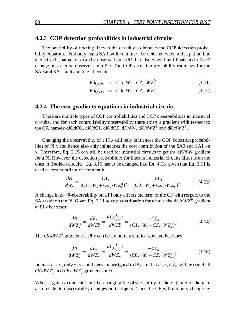
98 CHAPTER 4. TEST POINT INSERTION FOR BIST
4.2.3 COP detection probabilities in industrial circuits
The possibility of floating lines in the circuit also impacts the COP detection proba-bility equations. Not only can a SA0 fault on a line l be detected when a 0 is put on lineand a 0↔1 change on l can be observed on a PO, but also when line l floats and a Z↔0change on l can be observed on a PO. The COP detection probability estimates for theSA0 and SA1 faults on line l become:
Pdl/SA0 = C1l ·Wl +CZl ·WZ0l (4.11)
Pdl/SA1 = C0l ·Wl +CZl ·WZ1l (4.12)
4.2.4 The cost gradients equations in industrial circuits
There are multiple types of COP controllabilities and COP observabilities in industrialcircuits, and for each controllability/observability there exists a gradient with respect tothe CF, namely dK/dC0 , dK/dC1, dK/dCZ, dK/dW , dK/dWZ0 and dK/dWZ1.
Changing the observability of a PI x still only influences the COP detection probabil-ities of PI x and hence also only influences the cost contribution of the SA0 and SA1 onx. Therefore, Eq. 3.15 can still be used for industrial circuits to get the dK/dWx gradientfor a PI. However, the detection probabilities for lines in industrial circuits differ from theones in Boolean circuits. Eq. 3.16 has to be changed into Eq. 4.13, given that Eq. 3.11 isused as cost contribution for a fault.
dKdWx
=−C1x
(C1x ·Wx +CZx ·WZ0x )2 +
−C0x
(C0x ·Wx +CZx ·WZ1x )2 (4.13)
A change in Z↔0-observability on a PI only affects the term of the CF with respect to theSA0 fault on the PI. Given Eq. 3.11 as cost contribution for a fault, the dK/dWZ0 gradientat PI x becomes:
dKdWZ0
x=
dKx
dWZ0x
=d( 1
Pdx/0)
dWZ0x
=−CZx
(C1x ·Wx +CZx ·WZ0x )2 (4.14)
The dK/dWZ1 gradient on PI x can be found in a similar way and becomes:
dKdWZ1
x=
dKx
dWZ1x
=d( 1
Pdx/1)
dWZ1x
=−CZx
(C0x ·Wx +CZx ·WZ1x )2 (4.15)
In most cases, only zeros and ones are assigned to PIs. In that case, CZx will be 0 and alldK/dWZ0
x and dK/dWZ1x gradients are 0.
When a gate is connected to PIs, changing the observability of the output z of the gatealso results in observability changes on its inputs. Thus the CF will not only change by

4.2. COP FOR INDUSTRIAL CIRCUITS 99
the terms with respect to the SA0 and SA1 fault on line z, but also by the observabilitychanges on the inputs of the gate. Since it is known how the cost changes with respectto observability changes on the inputs (e.g., PIs), it is possible to apply a chain-rule tocompute the dK/dW , dK/dWZ0 and dK/dWZ1 values of gate output z and the observabilitygradients for internal nodes in the CUT become:
dKdWz
=dKz
dWz(4.16)
+X
∑i=1
(
dKdWxi
dWxi
dWz+
dKdWZ0
xi
dWZ0xi
dWz+
dKdWZ1
xi
dWZ1xi
dWz
)
dKdWZ0
z=
dKz
dWZ0z
(4.17)
+X
∑i=1
(
dKdWxi
dWxi
dWZ0z
+dK
dWZ0xi
dWZ0xi
dWZ0z
+dK
dWZ1xi
dWZ1xi
dWZ0z
)
dKdWZ1
z=
dKz
dWZ1z
(4.18)
+X
∑i=1
(
dKdWxi
dWxi
dWZ1z
+dK
dWZ0xi
dWZ0xi
dWZ1z
+dK
dWZ1xi
dWZ1xi
dWZ1z
)
A change in C0 on a PO z only affects the cost term with respect to the SA1 fault on POz (it is assumed that C1 and CZ remain the same). Similarly, a change in C1 only affectsthe cost term with respect to the SA0 fault. On POs, a change in CZ has no influence onthe SA0 or SA1 fault detectabilities and hence no influence on the cost contribution of theSA0 and SA1 faults on PO z. Because we assume that a Z value cannot be observed on aPO, Eqs. 4.11 and 4.12 on PO z reduce to:
Pdz/SA1 = C0z ·Wz (4.19)
Pdz/SA0 = C1z ·Wz (4.20)
Using these detection probability equations, the dK/dC0, dK/dC1 and dK/dCZ gradi-ent values on PO z become:
dKdC0z
=dKz/SA1
dC0z=
d( 1Pdz/SA1
)
dC0z=
−Wz
(C0z ·Wz)2 (4.21)
dKdC1z
=dKz/SA0
dC1z=
d( 1Pdz/SA0
)
dC1z=
−Wz
(C1z ·Wz)2 (4.22)
dKdCZz
= 0 (4.23)
A controllability change on input x j of gate a does not only influence the detection prob-ability of that input, but possibly also all the observabilities of the other inputs and the

100 CHAPTER 4. TEST POINT INSERTION FOR BIST
controllabilities on the output(s) of the gate and thus influences the detection probabilitiesant the cost contribution of the faults on the inputs and inputs of the gate. Therefore thegradient equations become:
dKdC0x j
=dKx j/SA1
dC0x j
(4.24)
+X
∑i=1,i6= j
(
dKdWxi
dWxi
dC0x j
+dK
dWZ0xi
dWZ0xi
dC0x j
+dK
dWZ1xi
dWZ1xi
dC0x j
)
+Z
∑k=1
(dK
dC0zk
dC0zk
dC0x j
+dK
dC1zk
dC1zk
dC0x j
+dK
dCZzk
dCZzk
dC0x j
)
dKdC1x j
=dKx j/SA0
dC1x j
(4.25)
+X
∑i=1,i6= j
(
dKdWxi
dWxi
dC1x j
+dK
dWZ0xi
dWZ0xi
dC1x j
+dK
dWZ1xi
dWZ1xi
dC1x j
)
+Z
∑k=1
(dK
dC0zk
dC0zk
dC1x j
+dK
dC1zk
dC1zk
dC1x j
+dK
dCZzk
dCZzk
dC1x j
)
dKdCZx j
=dKx j/SA0
dCZx j
+dKx j/SA1
dCZx j
(4.26)
+X
∑i=1,i6= j
(
dKdWxi
dWxi
dCZx j
+dK
dWZ0xi
dWZ0xi
dCZx j
+dK
dWZ1xi
dWZ1xi
dCZx j
)
+Z
∑k=1
(dK
dC0zk
dC0zk
dCZx j
+dK
dC1zk
dC1zk
dCZx j
+dK
dCZzk
dCZzk
dCZx j
)
The first part (the first line of each equation) represent the change with respect to thedetection probabilities on line x j. The second part of the equations (the second line)represents the change in the cost with respect to all possible observability changes on theother inputs due to the controllability change on line x j. The third part (the last line)represents the change in the cost with respect to all possible controllability changes onthe outputs due to the controllability change on line x j.
4.3 Proposed TPI for BIST algorithm for industrial cir-cuits
As described in Subsection 4.1.2, the HCRF TPI algorithm has been chosen as a basefor further TPI development. In Chapter 3, it has been described that in the IC industry(extra) SFFs are used to control and observe the TPs. Using transparent SFFs (TSFF) asTPs removes the necessity of using extra AND/OR gates for CPs. TSFFs also have the
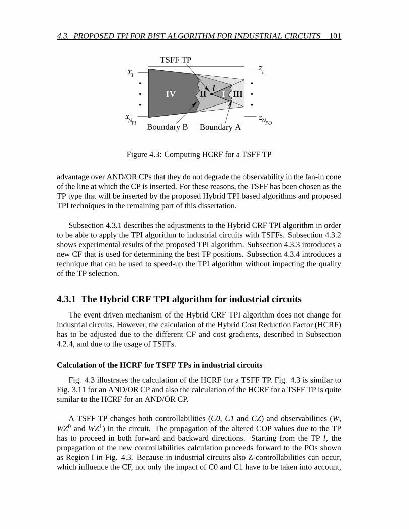
4.3. PROPOSED TPI FOR BIST ALGORITHM FOR INDUSTRIAL CIRCUITS 101
II III
z
x
x
z1
NPI NPO
1
l
TSFF TP
Boundary B Boundary A
IV I
Figure 4.3: Computing HCRF for a TSFF TP
advantage over AND/OR CPs that they do not degrade the observability in the fan-in coneof the line at which the CP is inserted. For these reasons, the TSFF has been chosen as theTP type that will be inserted by the proposed Hybrid TPI based algorithms and proposedTPI techniques in the remaining part of this dissertation.
Subsection 4.3.1 describes the adjustments to the Hybrid CRF TPI algorithm in orderto be able to apply the TPI algorithm to industrial circuits with TSFFs. Subsection 4.3.2shows experimental results of the proposed TPI algorithm. Subsection 4.3.3 introduces anew CF that is used for determining the best TP positions. Subsection 4.3.4 introduces atechnique that can be used to speed-up the TPI algorithm without impacting the qualityof the TP selection.
4.3.1 The Hybrid CRF TPI algorithm for industrial circuits
The event driven mechanism of the Hybrid CRF TPI algorithm does not change forindustrial circuits. However, the calculation of the Hybrid Cost Reduction Factor (HCRF)has to be adjusted due to the different CF and cost gradients, described in Subsection4.2.4, and due to the usage of TSFFs.
Calculation of the HCRF for TSFF TPs in industrial circuits
Fig. 4.3 illustrates the calculation of the HCRF for a TSFF TP. Fig. 4.3 is similar toFig. 3.11 for an AND/OR CP and also the calculation of the HCRF for a TSFF TP is quitesimilar to the HCRF for an AND/OR CP.
A TSFF TP changes both controllabilities (C0, C1 and CZ) and observabilities (W,WZ0 and WZ1) in the circuit. The propagation of the altered COP values due to the TPhas to proceed in both forward and backward directions. Starting from the TP l, thepropagation of the new controllabilities calculation proceeds forward to the POs shownas Region I in Fig. 4.3. Because in industrial circuits also Z-controllabilities can occur,which influence the CF, not only the impact of C0 and C1 have to be taken into account,

102 CHAPTER 4. TEST POINT INSERTION FOR BIST
but also the impact of CZ on the cost. During the processing of each gate input xgate, theratio of dK/dC0xgate ·∆C0xgate + dK/dC1xgate ·∆C1xgate + dK/dCZxgate ·∆CZxgate to K(Org) iscompared with a given user-defined threshold to decide whether the controllabilities inits fan-out cone should be calculated or that the controllability gradients can be used toestimate the impact on the cost. ∆C0xgate , ∆C1xgate and ∆CZxgate represent the change inzero controllability, respectively one controllability and Z controllability, of input xgate
due to the TP.After the forward propagation, a set of lines is obtained indicated as Boundary A in
Fig. 4.3. These lines are used as starting points for the backward propagation of the ob-servability changes to the PIs, similar to the calculation of the HCRF for OPs. This setof boundary lines can be seen as a set of pseudo-OPs. Line l is also added to this set ofpseudo-OPs, because the observabilities on l are changed due to the inserted TSFF TP,which is both a CP and an OP.
In industrial circuits not only the 0↔1 observability changes (∆W ) impact the CF, butalso the Z↔0 and Z↔1 observability changes (∆WZ0) and ∆WZ1). Therefore the ratioof dK/dWx ·∆Wx+dK/dWZ0
x ·∆WZ0x + dK/dWZ1
x ·∆WZ1x to K(Org) for each pseudo-OP is
checked with a user-defined threshold to determine whether the explicit observability cal-culations (and hence detectability probability and cost calculations) have to be propagatedbackward any further. The backward calculation stops when this ratio becomes below thisuser-defined threshold. The set of lines where the backward calculation stops is indicatedas Boundary B in Fig. 4.3 The observability gradients of the lines on Boundary B areused to estimate the cost impact on the remaining part of the circuit.
Given Eq. 3.11, the HCRF for a TSFF on line l comprises the following four parts:
1. ∑ f
(
1Pd f
(Org) −1
Pd f(m)
)
for every fault f inside Regions I and II.
The new controllabilities (C0, C1 and CZ) and observabilities (W, WZ0 and WZ1)of the lines corresponding to the faults in Regions I and II and therefore the newdetection probabilities and cost contributions of the faults are computed explicitly.They are computed using the above mentioned event-driven procedures.
2. ∑lbA∈Boundary A
(dK
dC0lbA·∆C0lbA + dK
dC1lbA·∆C1lbA + dK
dCZlbA·∆CZlbA
)
for every fault in
Region III.The controllability gradients of the lines lbA on Boundary A are used to estimate
∑ f∈Region III
(
1Pd f
(Org) −1
Pd f(m)
)
.
3. ∑lbB∈Boundary B
(
dKdWlbB
·∆WlbB + dKdWZ0
lbB
·∆WZ0lbB
+ dKdWZ1
lbB
·∆WZ1lbB
)
for every fault
in Region IV.The observability gradients of the lines lbB on Boundary B are used to estimate
∑ f∈Region IV
(
1Pd f
(Org) −1
Pd f(m)
)
.

4.3. PROPOSED TPI FOR BIST ALGORITHM FOR INDUSTRIAL CIRCUITS 103
4. The contribution of the new faults introduced by the inserted TSFF TP are added:1
Pdl′/SA0and 1
Pdl′/SA1. These are the SA0/SA1 faults on the TSFF output, see Fig.
3.4.d.
The equations to compute the HCRF for TSFF TPs become:
HCRFl = ∑f∈Regions I&II
(
1
Pd f(Org)
−1
Pd f(m)
)
−
(1
Pdl′/SA0+
1Pdl′/SA1
)
(4.27)
− ∑lbA∈Boundary A
(dK
dC0lbA
·∆C0lbA +dK
dC1lbA
·∆C1lbA +dK
dCZlbA
·∆CZlbA
)
− ∑lbB∈Boundary B
(
dKdWlbB
·∆WlbB +dK
dWZ0lbB
·∆WZ0lbB
+dK
dWZ1lbB
·∆WZ1lbB
)
The Hybrid CRF TPI algorithm for industrial circuits consists of the following sevensteps:
Step 1: TP candidate lines determinationThere are lines in the circuit which should be excluded as TP candidate, i.e. no TPsshould be inserted at lines which can and should be able to float. TPs at such linescould result in bus-conflicts. Also neither TPs should be inserted at the control linesfor bus-drivers nor at user-defined paths, e.g., critical paths or other “don’t touch”paths.
Step 2: Fault-set determinationBefore TPI, the fault set that will define the CF and will impact the TPI process hasto be determined; all untestable and collapsed faults are removed from the fault set.
Step 3: Determine COP TA values, cost and cost gradientsThe COP TA measures and gradients for each line, and cost values for each fault inthe circuit are calculated. Only faults which are in the fault set that contribute to theCF, as determined in Step 2, will get a non-zero cost contribution.
Step 4: Determine whether a TP should be insertedThe TPI process will only insert TPs when the cost is larger than a user-defineddesired maximum cost and the number of already inserted TPs is smaller than themaximum number of TPs that are allowed to be inserted into the circuit.
Step 5: Calculate HCRF valuesFor each TP candidate line, the HCRFs for TSFF TPs are calculated.
Step 6: Insert a TP at the line with the highest HCRF valueInsert a TSFF at the line with the highest HCRF value when the highest HCRF valuein the circuit is larger than the minimum required cost reduction for the insertion ofa TP.

104 CHAPTER 4. TEST POINT INSERTION FOR BIST
Step 7: Insert next TP or stopIf a TP has been inserted, go back to Step 3 and insert more TPs, when necessary.If no TP has been inserted, the Hybrid CRF TPI for industrial circuits is finished,and the current circuit is returned.
In Step 4, the cost is compared with a user-defined desired cost. When the cost becomesbelow the desired cost, it is assumed that the fault coverage will be high enough. Insteadof using this value, also a fault simulation run can be applied to the circuit with TPsto check whether the fault coverage is high enough. Although this is far more accuratethan checking if the cost is below a desired cost, a fault simulation run can be very timeconsuming and therefore, massively repeating fault simulation is not always applicablefor large industrial designs due to CPU time limitations.
4.3.2 Experimental results of the Hybrid CRF TPI algorithm for in-dustrial circuits
Tables A.5 and A.6 in Appendix A show the fault coverage and fault efficiency of sev-eral ISCAS’85 respectively ISCAS’89 circuits after the application of 32,000 PR patterns.Table 4.2 shows the fault coverages and efficiencies for these circuits after the applicationof 32,000 PR patterns when TSFF TPs have been inserted with the proposed Hybrid CRFTPI algorithm for industrial circuits [Geu97b, Geu03]. TPs only have been inserted intothe circuits that did not reach the 99% fault efficiency level without TPs. The experimentswere performed on a AMD Athlon XP 1600+ machine, with 512MB DDR RAM memoryrunning RedHat Linux 7.3.
Column Circuit lists the circuits name. Column Without TPs shows the number of ap-plied PR patterns (T ), the fault coverage (FC(%)) and the fault efficiency (FE(%)) for thelisted circuits before TPI. Column TPI shows the number of inserted TSFF TPs (TSFF )in the circuit and the CPU time spent on TPI (CPU). Column With TPs shows the numberof applied PR patterns (T), the fault coverage (FC(%)) and fault efficiency (FE(%)) for thecircuit with TPs. The rows Subtotal show the subtotals for the ISCAS’85, respectivelyISCAS’89 and ISCAS’89 addendum circuits. The fault coverages and efficiencies listedin these rows are weighted for the circuit size (ratio of the number of connections in thecircuit to the total number of connections in all circuits). The row Total shows the overallresults for the listed circuits.
Although the ISCAS benchmark do not contain three-state elements or fixed un-known input values, the Hybrid CRF TPI algorithm for industrial circuits is also applica-ble to these circuits. The TPI algorithm inserts TSFFs instead of AND/OR gates. Com-pared to the results given in Table 4.1, in general fewer TSFFs are inserted than CPs andOPs with the CRF TPI algorithm, the original Hybrid CRF TPI algorithm, or the MTPIalgorithm, while reaching the same or higher fault efficiencies. The proposed HybridCRF algorithm for industrial circuits only has to insert one single TSFF TP in order toreach 100% fault efficiency for circuit c2670, while the other algorithms require at least
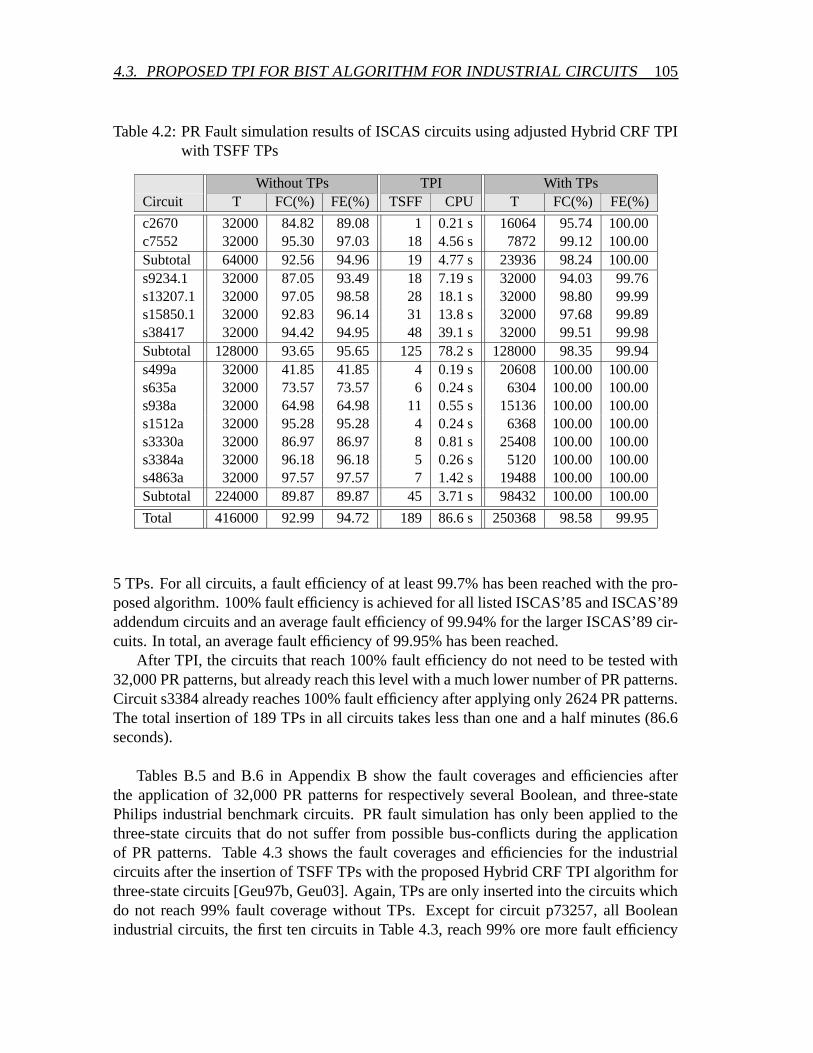
4.3. PROPOSED TPI FOR BIST ALGORITHM FOR INDUSTRIAL CIRCUITS 105
Table 4.2: PR Fault simulation results of ISCAS circuits using adjusted Hybrid CRF TPIwith TSFF TPs
Without TPs TPI With TPsCircuit T FC(%) FE(%) TSFF CPU T FC(%) FE(%)
c2670 32000 84.82 89.08 1 0.21 s 16064 95.74 100.00c7552 32000 95.30 97.03 18 4.56 s 7872 99.12 100.00Subtotal 64000 92.56 94.96 19 4.77 s 23936 98.24 100.00s9234.1 32000 87.05 93.49 18 7.19 s 32000 94.03 99.76s13207.1 32000 97.05 98.58 28 18.1 s 32000 98.80 99.99s15850.1 32000 92.83 96.14 31 13.8 s 32000 97.68 99.89s38417 32000 94.42 94.95 48 39.1 s 32000 99.51 99.98Subtotal 128000 93.65 95.65 125 78.2 s 128000 98.35 99.94s499a 32000 41.85 41.85 4 0.19 s 20608 100.00 100.00s635a 32000 73.57 73.57 6 0.24 s 6304 100.00 100.00s938a 32000 64.98 64.98 11 0.55 s 15136 100.00 100.00s1512a 32000 95.28 95.28 4 0.24 s 6368 100.00 100.00s3330a 32000 86.97 86.97 8 0.81 s 25408 100.00 100.00s3384a 32000 96.18 96.18 5 0.26 s 5120 100.00 100.00s4863a 32000 97.57 97.57 7 1.42 s 19488 100.00 100.00Subtotal 224000 89.87 89.87 45 3.71 s 98432 100.00 100.00
Total 416000 92.99 94.72 189 86.6 s 250368 98.58 99.95
5 TPs. For all circuits, a fault efficiency of at least 99.7% has been reached with the pro-posed algorithm. 100% fault efficiency is achieved for all listed ISCAS’85 and ISCAS’89addendum circuits and an average fault efficiency of 99.94% for the larger ISCAS’89 cir-cuits. In total, an average fault efficiency of 99.95% has been reached.
After TPI, the circuits that reach 100% fault efficiency do not need to be tested with32,000 PR patterns, but already reach this level with a much lower number of PR patterns.Circuit s3384 already reaches 100% fault efficiency after applying only 2624 PR patterns.The total insertion of 189 TPs in all circuits takes less than one and a half minutes (86.6seconds).
Tables B.5 and B.6 in Appendix B show the fault coverages and efficiencies afterthe application of 32,000 PR patterns for respectively several Boolean, and three-statePhilips industrial benchmark circuits. PR fault simulation has only been applied to thethree-state circuits that do not suffer from possible bus-conflicts during the applicationof PR patterns. Table 4.3 shows the fault coverages and efficiencies for the industrialcircuits after the insertion of TSFF TPs with the proposed Hybrid CRF TPI algorithm forthree-state circuits [Geu97b, Geu03]. Again, TPs are only inserted into the circuits whichdo not reach 99% fault coverage without TPs. Except for circuit p73257, all Booleanindustrial circuits, the first ten circuits in Table 4.3, reach 99% ore more fault efficiency
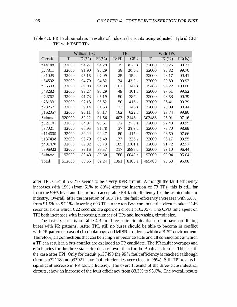
106 CHAPTER 4. TEST POINT INSERTION FOR BIST
Table 4.3: PR Fault simulation results of industrial circuits using adjusted Hybrid CRFTPI with TSFF TPs
Without TPs TPI With TPsCircuit T FC(%) FE(%) TSFF CPU T FC(%) FE(%)
p14148 32000 94.27 94.29 15 8.20 s 32000 99.26 99.27p27811 32000 91.90 96.29 38 20.0 s 32000 95.32 99.70p31025 32000 95.15 97.09 25 159 s 32000 98.17 99.41p34592 32000 94.79 94.82 34 43.2 s 32000 99.89 99.92p36503 32000 89.03 94.89 107 144 s 15488 94.22 100.00p43282 32000 93.27 95.29 49 101 s 32000 97.51 99.52p72767 32000 91.73 95.19 50 387 s 32000 96.58 99.39p73133 32000 92.13 95.52 50 413 s 32000 96.41 99.39p73257 32000 59.14 61.53 73 246 s 32000 78.09 80.44p162057 32000 96.11 97.17 162 622 s 32000 98.74 99.80Subtotal 320000 89.22 91.56 603 2146 s 303488 95.01 97.16p32118 32000 84.07 90.61 32 25.3 s 32000 92.48 98.95p37021 32000 67.95 91.78 37 28.3 s 32000 75.70 98.99p114605 32000 89.22 90.47 80 415 s 32000 96.59 97.66p137498 32000 93.79 95.49 137 323 s 32000 98.17 99.55p481470 32000 82.82 83.73 185 2361 s 32000 91.72 92.57p596922 32000 86.16 89.57 317 2886 s 32000 93.10 96.44Subtotal 192000 85.48 88.30 788 6040 s 192000 92.94 95.64
Total 512000 86.56 89.24 1391 8186 s 495488 93.53 96.08
after TPI. Circuit p73257 seems to be a very RPR circuit. Although the fault efficiencyincreases with 19% (from 61% to 80%) after the insertion of 73 TPs, this is still farfrom the 99% level and far from an acceptable PR fault efficiency for the semiconductorindustry. Overall, after the insertion of 603 TPs, the fault efficiency increases with 5.6%,from 91.5% to 97.1%. Inserting 603 TPs in the ten Boolean industrial circuits takes 2146seconds, from which 622 seconds are spent on circuit p162057. The CPU time spent onTPI both increases with increasing number of TPs and increasing circuit size.
The last six circuits in Table 4.3 are three-state circuits that do not have conflictingbuses with PR patterns. After TPI, still no buses should be able to become in conflictwith PR patterns to avoid circuit damage and MISR problems within a BIST environment.Therefore, all connections that can be at high impedance state and all connections at whicha TP can result in a bus-conflict are excluded as TP candidate. The PR fault coverages andefficiencies for the three-state circuits are lower than for the Boolean circuits. This is stillthe case after TPI. Only for circuit p137498 the 99% fault efficiency is reached (althoughcircuits p32118 and p37021 have fault efficiencies very close to 99%). Still TPI results insignificant increase in PR fault efficiency. The overall results of the three-state industrialcircuits, show an increase of the fault efficiency from 88.3% to 95.6%. The overall results
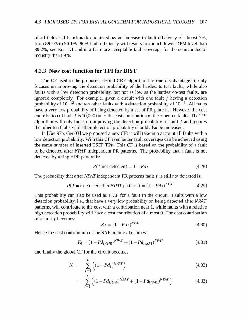
4.3. PROPOSED TPI FOR BIST ALGORITHM FOR INDUSTRIAL CIRCUITS 107
of all industrial benchmark circuits show an increase in fault efficiency of almost 7%,from 89.2% to 96.1%. 96% fault efficiency will results in a much lower DPM level than89.2%, see Eq. 1.1 and is a far more acceptable fault coverage for the semiconductorindustry than 89%.
4.3.3 New cost function for TPI for BIST
The CF used in the proposed Hybrid CRF algorithm has one disadvantage: it onlyfocuses on improving the detection probability of the hardest-to-test faults, while alsofaults with a low detection probability, but not as low as the hardest-to-test faults, areignored completely. For example, given a circuit with one fault f having a detectionprobability of 10−12 and ten other faults with a detection probability of 10−8. All faultshave a very low probability of being detected by a set of PR patterns. However the costcontribution of fault f is 10,000 times the cost contribution of the other ten faults. The TPIalgorithm will only focus on improving the detection probability of fault f and ignoresthe other ten faults while their detection probability should also be increased.
In [Geu97b, Geu03] we proposed a new CF; it will take into account all faults with alow detection probability. With this CF even better fault coverages can be achieved usingthe same number of inserted TSFF TPs. This CF is based on the probability of a faultto be detected after NPAT independent PR patterns. The probability that a fault is notdetected by a single PR pattern is:
P( f not detected) = 1−Pd f (4.28)
The probability that after NPAT independent PR patterns fault f is still not detected is:
P( f not detected after NPAT patterns) = (1−Pd f )NPAT (4.29)
This probability can also be used as a CF for a fault in the circuit. Faults with a lowdetection probability, i.e., that have a very low probability on being detected after NPATpatterns, will contribute to the cost with a contribution near 1, while faults with a relativehigh detection probability will have a cost contribution of almost 0. The cost contributionof a fault f becomes:
K f = (1−Pd f )NPAT (4.30)
Hence the cost contribution of the SAF on line l becomes:
Kl = (1−Pdl/SA0)NPAT +(1−Pdl/SA1)
NPAT (4.31)
and finally the global CF for the circuit becomes:
K =F
∑f =1
(
(1−Pd f )NPAT
)
(4.32)
=L
∑l=1
(
(1−Pdl/SA0)NPAT +(1−Pdl/SA1)
NPAT)
(4.33)

108 CHAPTER 4. TEST POINT INSERTION FOR BIST
A new CF results in new cost gradients. The chain-rules do not change, but the equationswith respect to the impact of the controllability/observability change on the cost contribu-tion of line l do. Given Eq. 4.31 the following equations are derived that should be usedin the cost gradient Eqs. 4.16-4.17 and 4.24-4.26:
dKz
dWz= −NPAT ·C1z · (1−Pdz/SA0)
NPAT−1 (4.34)
−NPAT ·C0z · (1−Pdz/SA1)NPAT−1
dKz
dWZ0z
= −NPAT ·CZz · (1−Pdz/SA1)NPAT−1 (4.35)
dKz
dWZ1z
= −NPAT ·CZz · (1−Pdz/SA0)NPAT−1 (4.36)
dKx j
dC0x j
= −NPAT ·Wx j · (1−Pdx j/SA1)NPAT−1 (4.37)
dKx j
dC1x j
= −NPAT ·Wx j · (1−Pdx j/SA0)NPAT−1 (4.38)
dKx j
dCZx j
= −NPAT ·WZ0x j· (1−Pdx j/SA0)
NPAT−1 (4.39)
−NPAT ·WZ1x j· (1−Pdx j/SA1)
NPAT−1
As a result, also the HCRF equation changes and becomes:
HCRFl = ∑f∈Regions I&II
(
(1−Pd(Org)f )NPAT − (1−Pd f
(m))NPAT)
(4.40)
−((1−Pdl′/SA0)
NPAT +(1−Pdl′/SA1)NPAT )
− ∑lbA∈Boundary A
(dK
dC0lbA
·∆C0lbA +dK
dC1lbA
·∆C1lbA +dK
dCZlbA
·∆CZlbA
)
− ∑lbB∈Boundary B
(
dKdWlbB
·∆WlbB +dK
dWZ0lbB
·∆WZ0lbB
+dK
dWZ1lbB
·∆WZ1lbB
)
Tables 4.4 and 4.5 show for several ISCAS, respectively industrial circuits, a comparisonof the PR fault coverages achieved after TPI with the original CF of Tsai et al.[Tsa97]and TPI with the new NPAT CF, the NPAT TPI algorithm [Geu97b, Geu03]. The value ofNPAT in CF 4.32 has been set to 32,000, the number of PR patterns that will be applied.In the Column Original cost function the number of applied PR patterns (NPAT ), the PR faultcoverages (FC (%)) and efficiencies (FE (%)) are shown in case the original CF is used. Inthe Column TPI with NPAT cost function, the number of inserted TPs (TSFF ), the CPU timespent on TPI (CPU) and the number of applied PR patterns (NPAT ), the PR fault coverages(FC (%)) and efficiencies (FE (%)) are shown for the NPAT TPI algorithm. The number ofTPs inserted with the NPAT CF is the same as with the original CF.
The original CF already resulted in very good fault efficiencies for the ISCAS bench-mark circuits as shown in Table 4.2. Except for the ISCAS’89 circuits, for all circuits

4.3. PROPOSED TPI FOR BIST ALGORITHM FOR INDUSTRIAL CIRCUITS 109
Table 4.4: Comparison of TPI with original and NPAT cost function for ISCAS circuits
Original cost function TPI with NPAT cost functionCircuit T FC(%) FE(%) TSFF CPU T FC(%) FE(%)
c2670 16064 95.74 100.00 1 0.25 s 16064 95.74 100.00c7552 7872 99.12 100.00 18 2.94 s 5280 99.17 100.00Subtotal 23936 98.24 100.00 19 3.19 s 21344 98.27 100.00s9234.1 32000 94.03 99.76 18 6.65 s 32000 94.08 99.83s13207.1 32000 98.80 99.99 28 20.8 s 32000 98.76 99.98s15850.1 32000 97.68 99.89 31 15.5 s 32000 97.72 99.92s38417 32000 99.51 99.98 48 40.7 s 32000 99.51 99.98Subtotal 128000 98.35 99.94 125 83.7 s 128000 98.36 99.95s499a 20608 100.00 100.00 4 0.18 s 15104 100.00 100.00s635a 6304 100.00 100.00 6 0.30 s 3456 100.00 100.00s938a 15136 100.00 100.00 11 0.39 s 5440 100.00 100.00s1512a 6368 100.00 100.00 4 0.29 s 24576 100.00 100.00s3330a 25408 100.00 100.00 8 0.60 s 25408 100.00 100.00s3384a 5120 100.00 100.00 5 0.31 s 2624 100.00 100.00s4863a 19488 100.00 100.00 7 0.48 s 19488 100.00 100.00Subtotal 98432 100.00 100.00 45 2.55 s 96096 100.00 100.00
Total 250368 98.58 99.95 189 89.4 s 245440 98.59 99.96
100% fault efficiency has been achieved. This does not change in case the NPAT CF isused. The fault coverage for circuit c7552 is higher with the NPAT CF than with the orig-inal CF while the fault efficiencies are 100% for both CFs. Hence the TPs inserted withNPAT TPI result in more untestable faults becoming testable after TPI than with the orig-inal CF for circuit c7552. Overall, the fault coverage and efficiency increases with 0.01%to 98.59% respectively 99.96% compared to the original circuit, while ±5000 fewer PRpatterns need to by applied to the circuit. The CPU time spent on TPI has increased with3 seconds from 86 seconds to 89 seconds. Overall, the differences between the two CFsare almost negligible for the ISCAS circuits.
The results for the industrial circuits given in Table 4.5 show more significant im-provement with the NPAT TPI algorithm. For the Boolean industrial circuits, the faultefficiencies increase overall from 97.16% to 97.38% and the fault coverages from 95.01%to 95.22%. For 6 of the 11 Boolean circuits, the fault efficiencies are lower with the NPATCF, but the differences are very very small, less than 0.1%. However the problem circuitwithin the Boolean industrial circuits, circuit p73257, clearly benefits from the NPAT CF.The fault efficiency increases with more than 2% which can be considered as a signif-icant improvement. Also the three-state industrial circuits clearly profit from this newCF, the fault efficiency increment is 1.16%, from 95.64 to 96.80%. Especially the largerthree-state circuits, p481470 and p596922, show significant improvement. These were the

110 CHAPTER 4. TEST POINT INSERTION FOR BIST
Table 4.5: Comparison of TPI with original and NPAT cost function for industrial circuits
Original cost function TPI with NPAT cost functionCircuit T FC(%) FE(%) TSFF CPU T FC(%) FE(%)
p14148 32000 99.26 99.27 15 9.08 s 32000 98.80 98.81p27811 32000 95.32 99.70 38 21.0 s 32000 95.40 99.78p31025 32000 98.17 99.41 25 197 s 32000 97.75 99.07p34592 32000 99.89 99.92 34 28.7 s 32000 99.94 99.95p36503 15488 94.22 100.00 107 135 s 32000 94.22 99.99p43282 32000 97.51 99.52 49 114 s 32000 97.52 99.51p72767 32000 96.58 99.39 50 448 s 32000 96.43 99.41p73133 32000 96.41 99.39 50 472 s 32000 96.46 99.37p73257 32000 78.09 80.44 73 159 s 32000 80.36 82.64p162057 32000 98.74 99.80 162 865 s 32000 98.61 99.67Subtotal 303488 95.01 97.16 603 2453 s 320000 95.22 97.38p32118 32000 92.48 98.95 32 33.4 s 32000 92.10 98.59p37021 32000 75.70 98.99 37 33.8 s 32000 75.48 98.76p114605 32000 96.59 97.66 80 404 s 32000 96.92 98.01p137498 32000 98.17 99.55 137 365 s 32000 98.21 99.63p481470 32000 91.72 92.57 185 2265 s 32000 93.52 94.10p596922 32000 93.10 96.44 317 3291 s 32000 94.55 97.87Subtotal 192000 92.94 95.64 788 6394 s 192000 94.19 96.80
Total 495488 93.53 96.08 1391 8848 s 512000 94.49 96.97
circuits with lower fault efficiencies than the other three-state circuits, so it is more impor-tant that their fault efficiencies were improved in order to be able to reach a high enoughtest quality with PR testing. Overall the fault efficiencies have been increased with almost1% from 96.08% to 96.97%. Especially the circuits with lower fault efficiencies (< 98%)with the original CF benefit more from the new CF than the circuit that already reach ahigh fault coverage(> 98%) with the original CF.
These results show that the NPAT CF seems to be more useful for three-state circuitsthan the original CF. The NPAT CF for a fault, Eq. 4.30, is slightly more CPU time con-suming than the original CF, Eq. 3.11. This can be seen in the CPU time spent on TPI.With the NPAT CF this increases from 8186 seconds to 8848 seconds.
4.3.4 CPU time reduction: Reduce the number of TP candidates
Not all lines in a circuit have to be considered as TP candidates. In Step 1 of the NPATTPI algorithm, given in Subsection 4.3.1, already all PIs, POs, and internal three-statelines are excluded as TP candidate. However, there are more lines that can be excluded inorder to reduce CPU time.

4.3. PROPOSED TPI FOR BIST ALGORITHM FOR INDUSTRIAL CIRCUITS 111
Table 4.6: Comparison results of TP candidates reduction for ISCAS circuits
No candidates reduction Candidates reductionCircuit TSFF FC(%) FE(%) CPU FC(%) FE(%) CPU
c2670 1 95.74 100.00 0.25 s 95.74 100.00 0.22 sc7552 18 99.17 100.00 2.94 s 99.17 100.00 2.38 sSubtotal 19 98.27 100.00 3.19 s 98.27 100.00 2.60 ss9234.1 18 94.08 99.83 6.65 s 94.03 99.77 4.21 ss13207.1 28 98.76 99.98 20.8 s 98.76 99.98 12.4 ss15850.1 31 97.72 99.92 15.5 s 97.73 99.94 10.2 ss38417 48 99.51 99.98 40.7 s 99.51 99.98 30.9 sSubtotal 125 98.36 99.95 83.7 s 98.35 99.95 57.7 ss499a 4 100.00 100.00 0.18 s 100.00 100.00 0.15 ss635a 6 100.00 100.00 0.30 s 100.00 100.00 0.19 ss938a 11 100.00 100.00 0.39 s 100.00 100.00 0.32 ss1512a 4 100.00 100.00 0.29 s 100.00 100.00 0.23 ss3330a 8 100.00 100.00 0.60 s 100.00 100.00 0.52 ss3384a 5 100.00 100.00 0.31 s 100.00 100.00 0.30 ss4863a 7 100.00 100.00 0.48 s 100.00 100.00 0.46 sSubtotal 45 100.00 100.00 2.55 s 100.00 100.00 2.17 s
Total 189 98.59 99.96 89.4 s 98.59 99.96 62.4 s
It is not necessary to take into account both the input and the output of an inverter/bufferas TP candidate. The observabilities, controllabilities and detectabilities are the sameat the inverter/buffer output as at the inverter/buffer input (except for the C0 ↔ C1 andPdSA0 ↔PdSA1 swap in case of an inverter). When the output of the inverter/buffer istestable, the input is testable too. It is enough to only consider the output of an in-verter/buffer as TP candidate.
Besides not taking into account inverter/buffer inputs as TP candidate, we have alsoexperimented in [Geu02a] with not taking into account fan-out branches as TP candidate.Only the fan-out stem will be considered TP candidate. This results in a significant reduc-tion of the number of TP candidates and hence in a reduction of the CPU time spent onTPI. However, excluding the fan-out branches can also impact the quality of TP selectionbecause no TPs are taken into account for faults that benefit from changed controllabili-ties of a single fan-out branch due to a TP at that fan-out branch.
Tables 4.6 and 4.7 show for the ISCAS circuits, respectively industrial circuits, theimpact of the TP candidates reduction on the fault coverages and CPU time spent on TPI[Geu02a]. Columns Circuit and TSFF show the name of the circuit, respectively the num-ber of inserted TSFFs TPs. Columns No candidates reduction and Candidates reduction showthe fault coverages (FC(%)), the fault efficiencies (FE(%)), and CPU time (CPU) spent on

112 CHAPTER 4. TEST POINT INSERTION FOR BIST
Table 4.7: Comparison results of TP candidates reduction for industrial circuits
No candidates reduction Candidates reductionCircuit TSFF FC(%) FE(%) CPU FC(%) FE(%) CPU
p14148 15 98.80 98.81 9.08 s 98.78 98.79 6.96 sp27811 38 95.40 99.78 21.0 s 95.40 99.78 16.7 sp31025 25 97.75 99.07 197 s 98.06 99.25 114 sp34592 34 99.94 99.95 28.7 s 99.93 99.95 20.4 sp36503 107 94.22 99.99 135 s 94.20 99.96 94.7 sp43282 49 97.52 99.51 114 s 97.54 99.53 77.2 sp72767 50 96.43 99.41 448 s 96.49 99.46 280 sp73133 50 96.46 99.37 472 s 96.47 99.38 295 sp73257 73 80.36 82.64 159 s 80.38 82.66 119 sp162057 162 98.61 99.67 865 s 98.61 99.68 634 sSubtotal 603 95.22 97.38 2453 s 95.25 97.40 1660 sp32118 32 92.10 98.59 33.4 s 92.16 98.64 23.7 sp37021 37 75.48 98.76 33.8 s 75.45 98.74 25.8 sp114605 80 96.92 98.01 404 s 97.06 98.15 278 sp137498 137 98.21 99.63 365 s 98.25 99.63 302 sp481470 185 93.52 94.10 2265 s 93.58 94.16 1695 sp596922 317 94.55 97.87 3291 s 94.56 97.89 2579 sSubtotal 788 94.19 96.80 6394 s 94.23 96.84 4905 s
Total 1391 94.49 96.97 8848 s 94.52 97.00 6566 s
TPI in case no TP candidates reduction, respectively TP candidates reduction takes place.The results in Table 4.6 show for the ISCAS circuits that there is almost no impact on
the fault coverage when TP candidates reduction has been used. Only for circuit s9234.1,the fault coverage and fault efficiency is 0.05%, respectively 0.06% less than without TPcandidates reduction. On the other hand, for circuit s15850.1 the fault coverage and faultefficiency slightly increase with 0.01%, respectively 0.02%. For the other circuits, thereis no visible impact on the fault coverage.
Although the impact on the fault coverage is hardly visible, the impact on the CPUtime spent on TPI is significant. The CPU time spent on TPI for the ISCAS circuits hasbeen reduced from 89.4s to 62.4s; which means a 30% reduction. The CPU time reductionis less for the smaller ISCAS circuits, i.e., the ISCAS’85 (19%) and ISCAS’89 addendum(15%) circuits, than for the larger ISCAS circuits, i.e., ISCAS’89 circuits (31%). Espe-cially for circuit s15850.1 a large reduction of 40% has been achieved.
The results of the industrial circuits given in Table 4.7 also show that there is notmuch impact on the fault coverage with TP candidates reduction. Overall, the fault cov-erage and fault efficiency do not reduce; they even increase with TP candidates reduction.Overall, the fault coverage and efficiency increase with 0.03%, the fault coverage from94.49% to 94.52% and the fault efficiency 96.97% to 97.00%. Again, although the impact
4.4. SUMMARY AND CONCLUSIONS 113
of TP candidates reduction is small on the PR fault coverage for the industrial circuits, theimpact on the CPU time spent on TPI is much more significant. The CPU time has beenreduced with 26% from 8848s to 6566s.
Hence the results of both the ISCAS and industrial circuits show that TP candidatesreduction has no negative impact on the quality of the TP selection, there is no structuralfault coverage reduction when TP candidates reduction is used. TP candidates reductioncan impact the fault coverage, both positive (improve) as negative(reduction) but the dif-ference is very small (in almost all cases less than 0.1%). On the other hand, the reductionin CPU time spent on TPI is substantial. CPU time reductions of ±30% can be achievedwithout impacting the quality of the TP selection.
4.4 Summary and conclusions
The MTPI BIST algorithm is commercially available and case studies have shown thatthe MTPI algorithm is applicable to industrial designs. But the MTPI algorithm has beendesigned to be used within the MTPI BIST scheme, depicted in Figure 3.13. Thereforeit cannot be used in combination with other BIST models and is only applicable for PRfault coverage for BIST. The CRF and HCRF TPI algorithm are not restricted to a singleBIST model or even to BIST, but they assume Boolean circuits and do not take intoaccount any implications with respect to Z and U values in industrial circuits. Becausethe HCRF TPI algorithm is fast, outperforms the CRF TPI algorithm, and results in goodPR fault coverage improvements after TPI, it has been chosen as a base for a new TPIalgorithm that can cope with industrial circuits and results in even better PR fault coverageimprovement after TPI. Extensions for COP TA measures, the CF and cost gradientshave been proposed such that the improved HCRF TPI algorithm can cope with industrialcircuits, containing possible Z and U values. SFFs are often used to drive CPs and observeOP outputs in (full-)scan circuits. Therefore the improved HCRF TPI algorithm insertsTSFFs such that the necessity of extra AND/OR gates for CPs is removed.
Experimental results of the HCRF TPI algorithm for industrial circuits, show thatgood PR fault coverage improvements can be achieved on both Boolean and three-statecircuits and is applicable to both small and large complex industrial designs.
A new CF has been proposed for the TPI algorithm. The proposed improved HybridCRF algorithm for industrial circuits with the new CF, called NPAT TPI algorithm resultsin even better PR fault coverage than the original CF of Tsai, especially for the industrialthree-state benchmark circuits.
In order to reduce the CPU time spent on NPAT TPI, a method has been introducedthat reduces the number of TP candidates in the circuits without impacting the quality ofthe TP selection. Experimental results show that with this technique a 30% reduction inCPU time can be achieved, while keeping the same PR fault coverage improvement (afterTPI) as without TP candidates reduction.

114 CHAPTER 4. TEST POINT INSERTION FOR BIST

CHAPTER 5
Test Point Insertion for compact SAFATPG
The increasing complexity of integrated circuits has a major impact on testing. Thedemands on the ATE become higher and higher, due to higher clock-frequencies and pincounts. This increasing complexity also results in larger ATPG test sets, resulting inhigher ATE vector memory requirements and longer test application times; both resultingin increasing test and ATE costs. In order to cope with the increasing complexity ofcircuits, faster testers with much more vector memory will be required, which will becomevery expensive. In the international technology road-map from the SIA [Sem01], it is evenexpected that without the necessary solutions, the ATE will not be able to cope with thedemands within only a few years.
An alternative to off-chip testing, using ATE, is on-chip testing; i.e., BIST, as de-scribed in Chapter 2. In many BIST implementations, a PRTPG is used to generate alarge number of PR patterns that will be applied to the circuit. But such PRTPGs fail todetect the RPR faults, resulting in lower achievable fault coverages; reducing the qualityof the test. In Chapter 4 it has been shown that the RPR problem can be solved by theinsertion of TPs. The inserted TPs improve the PR testability of the RPR faults within thecircuit.
TPI results in a reduction of the number of circuit inputs that have to be assigned inorder to test the (RPR) faults with PR patterns. But the same holds for ATPG; after theinsertion of a TP, also ATPG may have to assign fewer circuit inputs to find a pattern forthe (RPR) faults. Because fewer assigned inputs are required to detect faults in the circuitafter TPI, it becomes easier to combine patterns for different faults into one compact testpattern. When more tests for faults can be combined into one test pattern, overall, a morecompact test set can be obtained.
In this chapter it will be shown that TPI, even if only targeted at solving the RPRproblem (TPI for BIST), indeed results in more compact test sets for ATPG. However,sometimes a circuit is easily PR testable, while ATPG still does not result in a compacttest set. Therefore also new TPI techniques will be described that lead to even smaller test
115
116 CHAPTER 5. TEST POINT INSERTION FOR COMPACT SAF ATPG
sets than when using TPI for BIST for compact ATPG, and moreover, more consistentlyresults in a significant reduction of test set sizes.
Section 5.1 shows the impact of TPI for BIST on ATPG test set sizes. Section 5.2shows other TA measures that indicate if there are ATPG specific testability problemswith respect to compact ATPG test sets in a circuit. Section 5.3 introduces the CF weproposed in [Geu00] that takes into account these new TA measures in order to get evenbetter test set size reduction than with TPI for BIST. Although better test set size reductionhas been achieved with the CF proposed in Section 5.3, several circuits still suffer fromlarge test sets. They suffer from large fan-out free regions (FFRs). In Section 5.4, fourtechniques are described to reduce the sizes of large FFRs and hence, the ATPG testset sizes. Section 5.5 introduces a TPI pre-process that analyzes the TA measures of acircuit to find its specific testability problems. Given the results of the analysis, a CF willbe selected that is targeted at solving the hardest testability problem within that circuit.Experimental results in Section 5.5 will show that with the TPI pre-process, better ATPGtest set sizes can be achieved. Section 5.6 summarizes and concludes this chapter.
5.1 Impact of TPI for BIST on ATPG test set sizes
This section shows that even TPI for BIST, which is only targeted at improving the PRfault coverage of a circuit, can already result in significant ATPG test set size reduction.
Tables A.3 and A.4 in Appendix A show ATPG test set size information for the IS-CAS’85, respectively ISCAS’89, circuits without TPs. Tables B.3 and B.4 in AppendixB show ATPG test set size information for the Boolean industrial, respectively three-stateindustrial, benchmark circuits without TPs. The listed ATPG results in Appendices Aand B are compact ATPG results. This means that the ATPG already applies ATPG tech-niques [Kon96a] to get a very small ATPG test set. In the remainder of this dissertation,with ATPG is meant compact ATPG. TPI will only be performed on circuits that have anATPG test set size of more than 100 patterns. Circuits with smaller ATPG test set sizesare not candidate for TPI, because we consider their test set size to be small enough.
Tables 5.1 and 5.2 show experimental results of TPI for BIST (NPAT TPI) [Geu00]on compact ATPG test set sizes and ATPG generation times for several ISCAS and in-dustrial benchmark circuits. In case of TPI for PR BIST, the number of PR patterns thatwill be applied during test is normally known and this value is used in the NPAT TPIalgorithm as value for NPAT . In case of TPI for ATPG, the number of ATPG patterns inthe test after TPI is not known in advance, so what value of NPAT should be used? Thegoal is to get a very small test set. Therefore we have set the value of NPAT to 256, tosignal the NPAT TPI algorithm that the used test set is small and that the probability thatfaults are detected pseudo-randomly is low, because of the small test set.
Column ATPG without TPs shows the ATPG results for the circuits listed in ColumnCircuit without TPs; the ATPG test set size (T ), the ATPG fault coverage (FC(%)) and theCPU time spent on ATPG (CPU) are listed. Column TPI shows the number of inserted
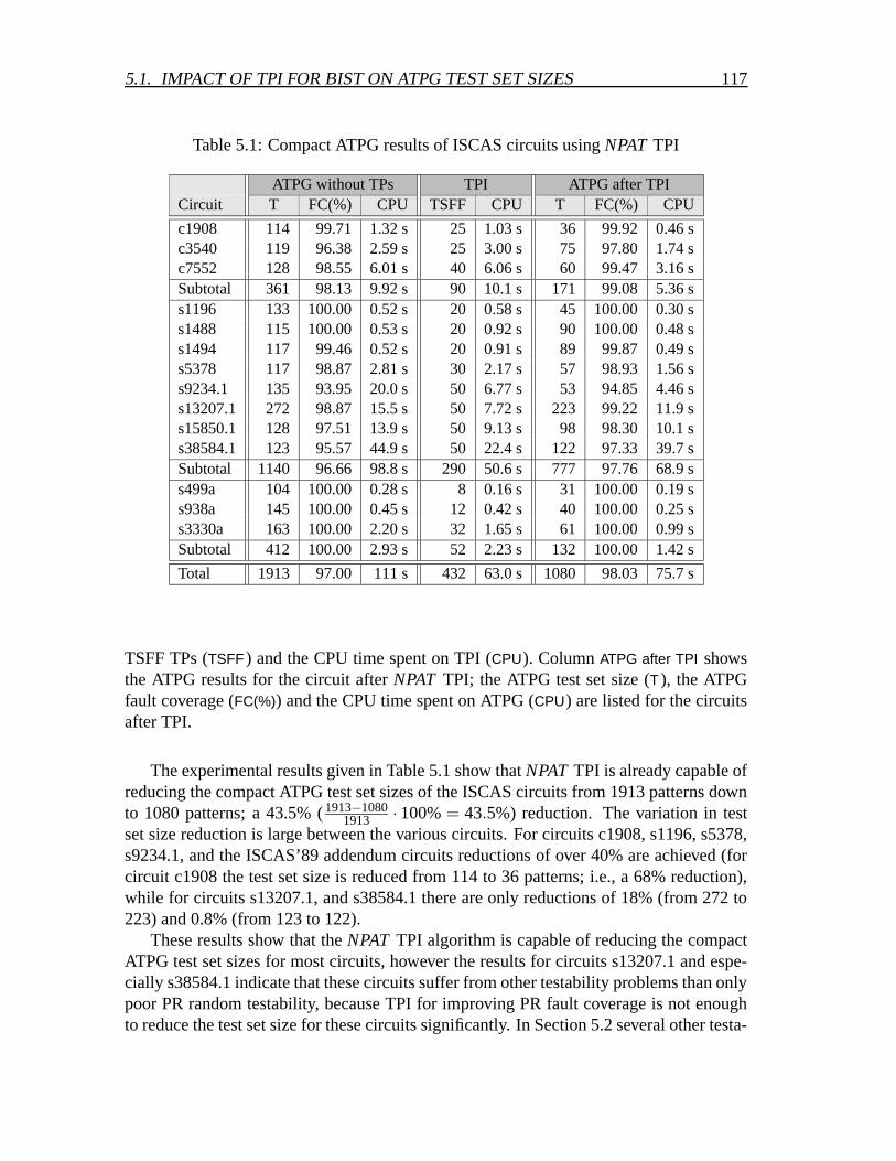
5.1. IMPACT OF TPI FOR BIST ON ATPG TEST SET SIZES 117
Table 5.1: Compact ATPG results of ISCAS circuits using NPAT TPI
ATPG without TPs TPI ATPG after TPICircuit T FC(%) CPU TSFF CPU T FC(%) CPU
c1908 114 99.71 1.32 s 25 1.03 s 36 99.92 0.46 sc3540 119 96.38 2.59 s 25 3.00 s 75 97.80 1.74 sc7552 128 98.55 6.01 s 40 6.06 s 60 99.47 3.16 sSubtotal 361 98.13 9.92 s 90 10.1 s 171 99.08 5.36 ss1196 133 100.00 0.52 s 20 0.58 s 45 100.00 0.30 ss1488 115 100.00 0.53 s 20 0.92 s 90 100.00 0.48 ss1494 117 99.46 0.52 s 20 0.91 s 89 99.87 0.49 ss5378 117 98.87 2.81 s 30 2.17 s 57 98.93 1.56 ss9234.1 135 93.95 20.0 s 50 6.77 s 53 94.85 4.46 ss13207.1 272 98.87 15.5 s 50 7.72 s 223 99.22 11.9 ss15850.1 128 97.51 13.9 s 50 9.13 s 98 98.30 10.1 ss38584.1 123 95.57 44.9 s 50 22.4 s 122 97.33 39.7 sSubtotal 1140 96.66 98.8 s 290 50.6 s 777 97.76 68.9 ss499a 104 100.00 0.28 s 8 0.16 s 31 100.00 0.19 ss938a 145 100.00 0.45 s 12 0.42 s 40 100.00 0.25 ss3330a 163 100.00 2.20 s 32 1.65 s 61 100.00 0.99 sSubtotal 412 100.00 2.93 s 52 2.23 s 132 100.00 1.42 s
Total 1913 97.00 111 s 432 63.0 s 1080 98.03 75.7 s
TSFF TPs (TSFF ) and the CPU time spent on TPI (CPU). Column ATPG after TPI showsthe ATPG results for the circuit after NPAT TPI; the ATPG test set size (T ), the ATPGfault coverage (FC(%)) and the CPU time spent on ATPG (CPU) are listed for the circuitsafter TPI.
The experimental results given in Table 5.1 show that NPAT TPI is already capable ofreducing the compact ATPG test set sizes of the ISCAS circuits from 1913 patterns downto 1080 patterns; a 43.5% ( 1913−1080
1913 · 100% = 43.5%) reduction. The variation in testset size reduction is large between the various circuits. For circuits c1908, s1196, s5378,s9234.1, and the ISCAS’89 addendum circuits reductions of over 40% are achieved (forcircuit c1908 the test set size is reduced from 114 to 36 patterns; i.e., a 68% reduction),while for circuits s13207.1, and s38584.1 there are only reductions of 18% (from 272 to223) and 0.8% (from 123 to 122).
These results show that the NPAT TPI algorithm is capable of reducing the compactATPG test set sizes for most circuits, however the results for circuits s13207.1 and espe-cially s38584.1 indicate that these circuits suffer from other testability problems than onlypoor PR random testability, because TPI for improving PR fault coverage is not enoughto reduce the test set size for these circuits significantly. In Section 5.2 several other testa-

118 CHAPTER 5. TEST POINT INSERTION FOR COMPACT SAF ATPG
Table 5.2: Compact ATPG results of industrial circuits using NPAT TPI
ATPG without TPs TPI ATPG after TPICircuit T FC(%) CPU TSFF CPU T FC(%) CPU
p7653 334 99.48 14.9 s 15 2.85 s 153 99.63 8.25 sp14148 385 99.99 30.0 s 15 3.48 s 218 100.00 17.4 sp27811 200 95.21 42.8 s 38 12.8 s 168 95.29 32.7 sp31025 714 97.90 307 s 25 16.6 s 449 98.67 129 sp34592 243 99.88 142 s 34 17.0 s 162 99.98 56.1 sp36503 175 97.20 71.3 s 30 14.4 s 110 97.22 37.1 sp43282 382 97.66 207 s 49 28.0 s 207 97.70 123 sp43663 194 99.23 58.8 s 50 21.9 s 98 99.25 36.0 sp72767 438 96.31 1527 s 50 57.7 s 311 96.65 409 sp73133 407 96.37 1492 s 50 59.2 s 301 96.73 405 sp73257 2097 98.06 1030 s 73 71.8 s 2132 98.06 1030 sp75344 273 99.18 153 s 55 45.9 s 196 99.25 114 sp162057 2055 98.51 926 s 162 290 s 556 98.78 330 sSubtotal 7897 97.95 6005 s 646 641 s 5061 98.15 2731 sp32118 570 93.50 131 s 32 13.5 s 263 93.53 39.8 sp37021 531 76.89 56.1 s 37 16.4 s 136 77.28 21.3 sp66171 2042 96.79 576 s 66 102 s 1792 96.79 580 sp71553 138 96.69 295 s 71 69.6 s 76 96.61 395 sp93140 511 93.81 1139 s 93 107 s 367 94.25 616 sp104649 1031 98.96 847 s 104 126 s 785 99.37 394 sp114605 689 98.44 827 s 80 127 s 513 98.64 520 sp137498 446 98.66 308 s 137 205 s 276 98.82 199 sp481470 1679 99.23 16560 s 185 942 s 1671 99.25 12400 sp596922 2038 96.87 8887 s 317 1895 s 2100 96.89 9475 sp598004 2129 98.70 5051 s 100 633 s 1942 98.77 3006 sp705050 655 76.76 8463 s 250 1749 s 530 91.47 4942 sp824184 2066 96.54 130153 s 300 2470 s 1114 96.73 24468 sp854266 565 97.54 6881 s 300 2613 s 359 97.62 5741 sSubtotal 15090 94.29 180180 s 2072 11073 s 11924 96.58 62803 s
Total 22987 94.76 186185 s 2718 11715 s 16985 96.78 65535 s
bility problems that cause large test sets will be described, including a description of howTPI can help reducing these testability problems.
The overall ATPG fault coverage for the ISCAS circuits has been increased from97% without TPs, to 98% with TPs. This can be considered as a significant improve-ment; 33% of the faults that were first not detected by the ATPG patterns become de-tected after TPI ((1− (100%−98%)
(100%−97%)) · 100% = 33%). Also after TPI, the CPU time spenton ATPG has decreased significantly; in total over all ISCAS circuits: from 111 sec-
5.2. TESTABILITY ANALYSIS MEASURES FOR DETECTING SPECIFICATPG/TEST SET SIZE PROBLEMS 119
onds circuits without TPs to 75.7 seconds with TPs. This means a reduction of 31.8%( (111−75.7)
111 · 100% = 31.8%). Hence, TPI for BIST on the ISCAS circuits results in asignificant ATPG test set size reduction, fault coverage improvement and CPU time re-duction.
The experimental results of Table 5.2 also show that significant test set size reductionscan been achieved with NPAT TPI for the industrial benchmark circuits. The total numberof compact ATPG test patterns for the Boolean industrial circuits is reduced from 7897patterns to 5061, a 35.9% reduction ( 7898−5061
7898 · 100% = 35.9%). The total number ofcompact ATPG test patterns for the three-state circuits is reduced from 15090 to 11924patterns, or 21.0% reduction. The reduction for circuit p598004 is relatively small, only187 patterns or 8.7%, while the number of patterns for circuit p596992 even increase.NPAT TPI for ATPG test set size reduction does not work very well on these circuits. Thereason for this is explained in the following sections. In total over all industrial bench-mark circuits, the number of ATPG patterns is reduced from 22987 to 16985, or 26.1%reduction.
The fault coverage for the Boolean circuits only slightly increases with 0.20% from97.95% to 98.15%, while for the three-state circuits, there is a very significant fault cov-erage improvement from 94.29% to 96.58%. This means that 40% of the faults that werenot covered for the three-state circuits without TPs become covered by ATPG patternsafter TPI ((1− (100%−96.58%)
(100%−94.29%)) · 100% = 40%). For all industrial benchmark circuits, theATPG fault coverage improves from 94.76% without TPs to 96.78% with TPs, or 38.5%of the faults that were not dectected by ATPG patterns without TPs become detected afterTPI.
The CPU time spent on compact ATPG is also significantly reduced after TPI. In caseof the Boolean industrial circuits, the CPU time is reduced from 6005 seconds to 2731seconds or 54.5% reduction. For the three-state circuits, the reduction even is 65.1%,from 180180 seconds to 62803 seconds. Especially the reduction for circuit p824184 isremarkable. For this circuit the CPU time spent on ATPG is reduced with 81.2%. Overallindustrial benchmark circuits, the CPU time reduction is 64.8%.
5.2 Testability analysis measures for detecting specificATPG/test set size problems
Besides COP, other TA measures exist that can help to indicate if there are testabilityproblems in the circuit that can cause a large test set. The TA measures SCOAP [Gol80]and test counts (TCs) [Hay74] can also be used to find testability problems. These TAmeasures are described in Subsections 5.2.1 and 5.2.2.

120 CHAPTER 5. TEST POINT INSERTION FOR COMPACT SAF ATPG
5.2.1 SCOAP
Sandia Controllability/Observability Analysis Program (SCOAP) is a TA measure thatis used by commercial ATPG tools, i.e., used in AMSAL (Appendix E). Similar to COP,SCOAP divides the measures in controllability and observability measures. The SCOAPcontrollability of a signal line is an estimate for the number of inputs that have to beassigned in order to get a 0(1) on the line. The SCOAP observability of a line is anestimate for the number of inputs that have to be set to propagate a fault-effect from thatline to an output. Besides the number of inputs that have to be set, SCOAP also takes intoaccount how ’deep’(level) the line is in the circuit and the number of fan-out branches thatwill also be assigned due to the input assignments.
ATPGs try to choose the paths with the smallest SCOAP values to activate faults andto propagate fault effects to POs, because the SCOAP values suggest that these pathsrequire the fewest number of input assignments. When TPI is used to reduce the SCOAPvalues for lines, the ATPG can generate test patterns with fewer assigned inputs for thefaults corresponding to these lines. More test patterns can be compacted into one singletest pattern, resulting in a better test set size reduction. Because SCOAP values also takeinto account the level of signal lines and the number of fan-out branches, they are oftenfar from exact with respect to the necessary input assignments in order to activate faults orpropagate fault-effect. However, they give a good indication how difficult it is to controla signal line or to make it observable compared to other signal lines.
5.2.2 Test counts
In [Hay74] and [Kri87], a method is presented to find a lower bound on the test setsize for a circuit such that all SAFs can be detected. In order to get this lower bound, theTA measures test counts (TCs) are calculated for each line in the circuit. They consist ofthe following two types of values:
1. The essential zeros (ones), E0(E1):The minimum number of times a line must become 0(1) (during the application ofa test set) and be observable on an output, such that all corresponding faults in itsfan-in cone can be covered..
2. The total zeros (ones), T0(T1):The minimum total number of times a line must become 0(1) (during the applicationof a test set) and either be observable or making other lines observable..
Because for each line l, a minimum of T 0l+T 1l patterns are necessary (T 0l patterns forthe minimum total number of times l must be 0 and T 1l patterns for the minimum totalnumber of times l must be 1), Eq. 5.1 can be used to calculate a lower bound on theminimum test set size, Tmin necessary for achieving complete fault coverage, in which Lrepresents the number of lines in the circuit.
Tmin ≥ maxLl=1(T 0l +T 1l) (5.1)
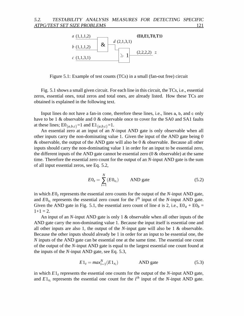
5.2. TESTABILITY ANALYSIS MEASURES FOR DETECTING SPECIFICATPG/TEST SET SIZE PROBLEMS 121
1
&d
z
a
b
c (1,1,3,1)
(1,1,1,2)
(1,1,1,2)(2,1,3,1)
(2,2,2,2)
(E0,E1,T0,T1)
Figure 5.1: Example of test counts (TCs) in a small (fan-out free) circuit
Fig. 5.1 shows a small given circuit. For each line in this circuit, the TCs, i.e., essentialzeros, essential ones, total zeros and total ones, are already listed. How these TCs areobtained is explained in the following text.
Input lines do not have a fan-in cone, therefore these lines, i.e., lines a, b, and c onlyhave to be 1 & observable and 0 & observable once to cover for the SA0 and SA1 faultsat these lines; E0{a,b,c}=1 and E1{a,b,c}=1.
An essential zero at an input of an N-input AND gate is only observable when allother inputs carry the non-dominating value 1. Given the input of the AND gate being 0& observable, the output of the AND gate will also be 0 & observable. Because all otherinputs should carry the non-dominating value 1 in order for an input to be essential zero,the different inputs of the AND gate cannot be essential zero (0 & observable) at the sametime. Therefore the essential zero count for the output of an N-input AND gate is the sumof all input essential zeros, see Eq. 5.2,
E0z =N
∑i=1
(E0xi) AND gate (5.2)
in which E0z represents the essential zero counts for the output of the N-input AND gate,and E0xi represents the essential zero count for the ith input of the N-input AND gate.Given the AND gate in Fig. 5.1, the essential zero count of line d is 2, i.e., E0a + E0b =1+1 = 2.
An input of an N-input AND gate is only 1 & observable when all other inputs of theAND gate carry the non-dominating value 1. Because the input itself is essential one andall other inputs are also 1, the output of the N-input gate will also be 1 & observable.Because the other inputs should already be 1 in order for an input to be essential one, theN inputs of the AND gate can be essential one at the same time. The essential one countof the output of the N-input AND gate is equal to the largest essential one count found atthe inputs of the N-input AND gate, see Eq. 5.3,
E1z = maxNi=1(E1xi) AND gate (5.3)
in which E1z represents the essential one counts for the output of the N-input AND gate,and E1xi represents the essential one count for the ith input of the N-input AND gate.

122 CHAPTER 5. TEST POINT INSERTION FOR COMPACT SAF ATPG
Given the AND gate in Fig. 5.1, the essential one count of line d is 1, i.e., max(E1a, E1b)= max(1,1) = 1.
The the essential zero counts and essential one counts equations for an N-input ORgate are derived in a similar way as for the AND gate and become:
E0z = maxNi=1(E0xi) OR gate (5.4)
E1z =N
∑i=1
(E1xi) OR gate (5.5)
Given Eqs. 5.4 and 5.5, the following essential counts for line z are obtained:E0z = max(E0c,E0d) = max(2,1) = 2; E1z = E1c +E1d = 1+1 = 2.
z is a circuit output, for which the total counts are always equal to the essential counts,hence T 0z=E0z and T 1z=E1z. In case of an N-input OR gate, the output of the gate canonly be 0 when all inputs are 0. Besides that, an input xi of the OR gate should alsocarry the non-dominating value 0 when the other inputs should be 1 & observable, i.e.,carry essential ones. Given this, the total zero count for an input xi of an OR gate can beobtained with Eq. 5.6.
T 0xi = T 0z +N
∑j=1, j 6=i
(E1x j) OR gate (5.6)
where T 0xi and T 0z are the total zero counts for OR gate input xi, respectively OR gateoutput z, and E1x j the essential one count for OR gate input x j. Given Eq. 5.6, line d
should not only be 0 when z should be 0, but also when c carries an essential one value;T 0d = T 0z + E1c = 2 + 1 = 3. Same applies to line c, it should not only be 0 when z
should be 0, but also when d carries an essential 1 value; T 0c = T 0z +E1d = 2+1 = 3.For an OR gate, it is not necessary for an input to be 1 when the output should be 1;
it is allowed to be 0 as long as there is another input that carries a 1. A 1 on an input ofthe OR gate will also not make other inputs of the OR gate observable, therefore the totalone count of an input of an OR gate is just the number of times that the input itself shouldbe 1 & observable. In other words, the total one counts of an input of an OR gate equalsthe essential one counts of that input, see Eq. 5.7.
T 1xi = E1xi OR gate (5.7)
Given Eq. 5.7, the total one counts for line c and d become: T 1c = E1c = 1,T 1d = E1d = 1.
The total counts equation for an AND gate are derived in a similar way as for the ORgate and are given in Eqs. 5.8 and 5.9.
T 0xi = E0xi AND gate (5.8)
T 1xi = T 1z +N
∑j=1, j 6=i
(E0x j) AND gate (5.9)

5.2. TESTABILITY ANALYSIS MEASURES FOR DETECTING SPECIFICATPG/TEST SET SIZE PROBLEMS 123
Given Eqs. 5.8 and 5.9, the total counts for lines a and b are obtained. T 0a = E0a = 1,T 1a = T 1d +E0b = 1+1 = 2, T 0b = E0b = 1, T 1b = T 1d +E0a = 1+1 = 2.
With Eq. 5.1, the lower bound on the test set size can be obtained. For the examplecircuit of Fig. 5.1, the found lower bound is 4.
Table 5.3 shows for all input patterns of the circuit given in Fig. 5.1 which faults willbe detected. The first three columns, Columns a, b and c represent the input patterns andthe remaining ten columns show for all SAFs at lines a, b, c, d and z if the given pat-tern covers (x) or does not cover (-) the fault. Given the fault coverage matrix of Table5.3, 3 minimum test sets of 4 patterns covering all faults are found. These three sets are:TS1={110, 010, 100, 001}, TS2={110, 010, 100, 011}, and TS3={110, 010, 100, 101}.In TS1 and TS2, a=0 occurs twice, while in TS3, a=0 only occurs 1. Hence, a should be0 at least once for complete coverage, which equals the total zero count of a calculatedbefore, T 0a = 1. In TS1 and TS2, a=1 occurs twice, while in TS3, a=1 even occurs threetimes. Hence a should be 1 at least twice for complete coverage, which equals the totalone count of a calculated before, T 1a = 2. In the same way the correctness of the totalcounts for lines b and c can be checked. Hence for this example circuit, the TCs are exactand the lower bound of the test set found with Eq. 5.1 equals the actual minimum test setsize.
The TC method is only exact for fan-out free circuits (the circuit given in Fig. 5.1is fan-out free), because it cannot be known in advance how the essential zeros/ones willdivide over the different fan-out branches during actual ATPG. Heuristics are necessary topredict how the TCs will divide over these branches. Section 5.3 will describe the heuris-tic that is used in our proposed TPI algorithm. In [Kri87], propagation of the essentialvalues over branches is ignored: each branch is assigned an E0/E1 value of 1.
Table 5.3: Fault coverage matrix for all fault in Fig. 5.1
Pattern Stuck-at 0 fault Stuck-at 1 faulta b c a b c d z a b c d z0 0 0 - - - - - - - x x x0 0 1 - - x - x - - - - -0 1 0 - - - - - x - x x x0 1 1 - - x - x - - - - -1 0 0 - - - - - - x x x x1 0 1 - - x - x - - - - -1 1 0 x x - x x - - - - -1 1 1 - - - - x - - - - -

124 CHAPTER 5. TEST POINT INSERTION FOR COMPACT SAF ATPG
When a circuit has lines with very large TC values, it will also have a very large ATPGtest set size, because T 0 + T 1 gives a lower bound on the necessary test set size in orderto cover all SAFs in the circuit. With a CF that takes TCs into account, the TPI algorithmwill reduce the TC values. With reduced TC values, also the lower bound on the minimumtest set size reduces, which makes smaller test sets possible.
5.3 Test counts in a TPI cost function
For circuits with (reconvergent) fan-out, the TCs are not very accurate, because it isnot known how the essential counts are divided over the fan-out branches. Therefore itwould not seem to be a good idea to only rely on the individual TCs to find the best TPpositions in the circuit in order to get more test set size reduction. Therefore TCs willonly be used as a guidance in selecting the right TP positions. In [Geu00], we proposed aCF that takes into account both COP and TC values, such that TPs will be selected on thebasis of minimizing a CF, hence both increasing PR detectability and reducing TC valuesin the circuit. Results in [Geu00] and [Geu01] have shown that by taking into accountTCs, better compact ATPG test set size reductions can be achieved, as will be describedin this section.
The following text illustrates the basic idea of the CF that takes into account bothCOP and TCs. Given that the following two lines are part of a circuit: Line a, with manyhard-to-test RPR faults in its input-cone and through which only one or two tests have topass, and line b with fewer hard-to-test RPR faults in its input-cone but through whichmany tests have to pass. It is assumed that these two lines are the only two TP candidates.
According to CFs that are only based on COP, e.g., Eqs. 3.11 and 4.30, the TPI al-gorithm will primarily focus on solving the PR testability problems for line a because itsfaults are the most hard-to-test. But for the ATPG this will mainly result in an easier gen-eration of only a few patterns. These patterns will have fewer assigned inputs, howeverthere are only a few of these patterns such that this will not have too much impact on thetotal test set size.
The proposed cost method based on TCs and COP however, will insert the TP at lineb. In spite of the fact that the faults in its input-cone are easier to test pseudo-randomlythan those of a, the cost contribution of b will be much higher because many tests (faulteffects) have to pass through b. A TP at b will probably result in a larger cost reductionthan at a. For the ATPG this means that many faults will be easier to detect and will havefewer inputs assigned in their tests. When there are many faults that require fewer inputsassigned in order to be detected, the impact on the compaction will be larger.
Subsection 5.3.1 introduces the proposed COP and TC based CF and the correspond-ing cost gradient value equations. Using TC values in the CF has a significant impact onthe Hybrid TPI algorithm. The consequences of the TC-based CF on the TPI algorithm

5.3. TEST COUNTS IN A TPI COST FUNCTION 125
are described in Subsection 5.3.2.
5.3.1 TC and COP based cost function
Eq. 5.10 shows the CF used in [Geu00]; it takes into account both COP and TC valuesand is based on the original HCRF CF for a line l [Tsa97], see Eq. 3.14.
Kl =E1l
C1l ·Wl+
T 1l −E1l
C1l+
E0l
C0l ·Wl+
T 0l −E0l
C0l(5.10)
This CF consists of the following four fractions:
1. The first fraction represents the number of times that line l should be essentialone, i.e., the minimum number of times that line l should be driven to 1 and beobservable at the same time, divided by the detection probability of the SA0 faultat l, i.e., the probability that line l is 1 & observable.
2. The second fraction represents the remaining minimum number of times that line lshould be driven to 1, i.e., should be 1 but not necessarily be observable (the totalone counts minus the essential one counts), divided by the probability that l is 1.
3. The third fraction represents the number of times that line l should be essentialzero, i.e., the minimum number of times that line l should be driven to 0 and beobservable at the same time, divided by the detection probability of the SA1 faultat l, i.e., the probability that line l is 0 & observable.
4. The last fraction represents the remaining minimum number of times the line shouldbe driven to 0, i.e., should be 0 but not necessarily be observable (the total zerocounts minus the essential zero counts), divided by the probability that l is 0.
This CF does not only take into account the probability of lines being 1(0) & observable(i.e., the detection probability), but also takes into account the minimum number of timesthat they should be 1(0) & observable (i.e., the TCs) to cover all faults in the fan-in coneof the line. In three-state circuits, essential Zs and total Zs can also occur, but there theyare very rare, therefore we have not taken them into account.
A new CF means new cost gradient equations that are used by the HCRF TPI algo-rithm, see Subsections 3.5.3 and 4.2.4. The chain-rule for the cost gradient calculationdoes not change, but the parts of the equations with respect to the impact of controllabil-ity/observability changes on the cost contribution of the line itself do change. Given theCF of Eq. 5.10, Eqs. 5.11-5.12 are the derived gradient equations with respect to observ-ability changes on gate output z, and Eqs. 5.14-5.16 are the derived gradient equationswith respect to controllability changes on gate input x j.
dKz
dWz= −
E0z
C0z ·W 2z−
E1z
C1z ·W 2z
(5.11)

126 CHAPTER 5. TEST POINT INSERTION FOR COMPACT SAF ATPG
dKz
dWZ0z
= 0 (5.12)
dKz
dWZ1z
= 0 (5.13)
dKx j
dC0x j
= −E0x j
C02x j·Wx j
+E0x j −T 0x j
C02x j
(5.14)
dKx j
dC1x j
= −E1x j
C12x j·Wx j
+E1x j −T 1x j
C12x j
(5.15)
dKx j
dCZx j
= 0 (5.16)
dK/dCZ, dK/dWZ0 and dK/dWZ1 are always 0, because this CF does not take into accountZ controllabilities, Z↔0 observabilities and Z↔1 observabilities. However, in three-state circuits, there will be non-zero Z controllabilities, Z↔0 or Z↔1 observabilities.Therefore the COP calculations and the cost gradient chain-rule will still have to take intoaccount these Z probabilities.
Because the CF does take into account TC measures and so will change when theTC measures change, there also exist cost gradients with respect to essential counts andtotal counts. The total counts cost gradients are derived in a similar way as the COPobservability cost gradients, see Subsection 3.5.3; they consist of a part with respect tothe total counts changes on a gate output z itself and a chain-rule for the total countschanges on the gate inputs caused by the changes at z. Eqs. 5.17 and 5.18 show the totalcounts cost gradients,
dKdT 0z
=dKz
dT 0z+
X
∑i=1
(dK
dT 0xi
dT 0xi
dT 0z+
dKdT 1xi
dT 1xi
dT 0z
)
(5.17)
dKdT 1z
=dKz
dT 1z+
X
∑i=1
(dK
dT 0xi
dT 0xi
dT 1z+
dKdT 1xi
dT 1xi
dT 1z
)
(5.18)
Given CF 5.10, the first part of the total counts cost gradients become:
dKz
dT 0z=
1C0z
(5.19)
dKz
dT 1z=
1C1z
(5.20)
and the total counts cost gradients become:
dKdT 0z
=1
C0z+
X
∑i=1
(dK
dT 0xi
dT 0xi
dT 0z+
dKdT 1xi
dT 1xi
dT 0z
)
(5.21)
dKdT 1z
=1
C1z+
X
∑i=1
(dK
dT 0xi
dT 0xi
dT 1z+
dKdT 1xi
dT 1xi
dT 1z
)
(5.22)

5.3. TEST COUNTS IN A TPI COST FUNCTION 127
The essential counts cost gradients are derived in a similar way as the COP controllabilitycost gradients, see Subsection 3.5.3; they consist of a part with respect to the essentialcounts changes on the gate input x j itself, a chain-rule for the essential counts changeson the Z gate output(s) caused by the changes at x j, and a chain rule for the total countschanges on the other X − 1 inputs of the gate caused by the essential counts changes onx j. Eqs. 5.23 and 5.24 show the essential counts cost gradients.
dKdE0x j
=dKx j
dE0x j
+X
∑i=1,i6= j
(dK
dT 0xi
dT 0xi
dE0x j
+dK
dT 1xi
dT 1xi
dE0x j
)
(5.23)
+Z
∑k=1
(dK
dE0zk
dE0zk
dE0x j
+dK
dE1zk
dE1zk
dE0x j
)
dKdE1x j
=dKx j
dE1x j
+X
∑i=1,i6= j
(dK
dT 0xi
dT 0xi
dE1x j
+dK
dT 1xi
dT 1xi
dE1x j
)
(5.24)
+Z
∑k=1
(dK
dE0zk
dE0zk
dE1x j
+dK
dE1zk
dE1zk
dE1x j
)
Given CF 5.10, the first part of the essential counts cost gradients become:
dKx j
dE0x j
=(1−Wx j)
C0x j ·Wx j
(5.25)
dKx j
dE1x j
=(1−Wx j)
C1x j ·Wx j
(5.26)
and the essential counts cost gradients become:
dKdE0x j
=(1−Wx j)
C0x j ·Wx j
+X
∑i=1,i6= j
(dK
dT 0xi
dT 0xi
dE0x j
+dK
dT 1xi
dT 1xi
dE0x j
)
(5.27)
+Z
∑k=1
(dK
dE0zk
dE0zk
dE0x j
+dK
dE1zk
dE1zk
dE0x j
)
dKdE1x j
=(1−Wx j)
C1x j ·Wx j
+X
∑i=1,i6= j
(dK
dT 0xi
dT 0xi
dE1x j
+dK
dT 1xi
dT 1xi
dE1x j
)
(5.28)
+Z
∑k=1
(dK
dE0zk
dE0zk
dE1x j
+dK
dE1zk
dE1zk
dE1x j
)
5.3.2 Implications of a TC based CF on the TPI algorithm
As mentioned in Subsection 5.2.2, TCs are only exact in fan-out free circuits, becauseit is not known how TC values will propagate over fan-out branches. In general all circuits

128 CHAPTER 5. TEST POINT INSERTION FOR COMPACT SAF ATPG
have fan-out branches, therefore before TCs can be used in the CF of the Hybrid TPIalgorithm, a heuristic must be established to divide the TC values over the different fan-out branches. As mentioned in Subsection 5.2.1, ATPGs use SCOAP values to choosewhich paths to take to activate or propagate fault effects. The lower the SCOAP valueof a line, the higher the probability that the ATPG will use that line to activate faultsor propagate fault effects. Therefore in [Geu00] we proposed to use a SCOAP basedheuristic to divide the essential counts over fan-out branches. The higher the SCOAPobservability of a fan-out branch, the less likely that essential counts will propagate overthat fan-out branch. The branch with the lowest SCOAP observability is assumed topropagate most of the essential counts. Given a fan-out stem x with L fan-out brancheszl , with each fan-out branch having a SCOAP observability SWzl , we use the followingheuristics for propagating the essential counts over the fan-out branches:
E0zl =
1SWzl
∑Li=1
1SWi
·E0x (5.29)
E1zl =
1SWzl
∑Li=1
1SWi
·E1x (5.30)
Because its more likely that essential values propagate over lines with smaller SCOAPobservability, we use 1
SW , such that 1SWzl
is larger for branches zl with smaller SCOAP val-
ues. The normalization with ∑Li=1
1SWi
is used such that the sum of the essential accountsover all branches does not exceed the essential count of the fan-out stem.
The event-driven algorithm to calculate the HCRF values for each TP candidate be-comes more complicated due to the TC based CF. Because the essential counts in thecircuit depend on the SCOAP observabilities, i.e., the propagation of the essential countsover fan-out branches depends on the SCOAP observability, an extra forward and back-ward propagation of cost changes is necessary in the event-driven HCRF algorithm, as isexplained in the following text.
The HCRF calculation given a TC based CF, like Eq. 5.10, can be divided into twosteps. The first step consists of the HCRF calculation for a non TC based CF, e.g., Eqs.3.11 and 4.30, as described in Subsection 4.3.1. In addition to the HCRF calculation for anon TC based CF, an extra step is necessary to take into account essential counts changesin the circuit due to SCOAP observability changes. Descriptions of these two steps aregiven in the following text:
Step 1 of the HCRF calculation given a TC based cost function
This first part of the calculation is depicted in Fig. 5.2(a). This figure is the same asFig. 4.3, which describes the HCRF calculation given a non TC based CF. The impact ofthe TP on the TA values, and hence on the cost reduction, differs for the four differently

5.3. TEST COUNTS IN A TPI COST FUNCTION 129
III
z
x
x
z1
NPI NPO
1
l
TSFF TP
Boundary B Boundary A
IV II I
(a) Propagation of TA measures changes
VIIIVI
VIIV
z
x
x
z1
NPI NPO
1
Boundary CBoundary D
Boundary B
l
(b) Propagation of TC changes due toSCOAP observability changes
Figure 5.2: Computing HCRF given a TC based cost function
shaded regions and is zero for the remaining (white) part of the circuit. These shadedregions and their different impacts are:
Region I: The part of the circuit in the fan-out cone of line l up to Boundary A inwhich the TSFF TP will cause significant changes in controllabilities and/or essen-tial counts.
Region II: The part of the circuit between Boundary A and Boundary B in which theTSFF TP will cause significant observabilities and/or total counts changes. RegionII includes Region I.
Region III: The part of the circuit between Boundary A and the POs in which theTSFF TP will only cause small changes in controllabilities, observabilities, essen-tial counts and total counts.
Region IV: The part of the circuit between the PIs and Boundary B in which the TSFFTP will only cause small changes in observabilities and total counts.
Related to Regions I-IV, the first step of the HCRF for a TSFF TP at line l comprises thefollowing four parts:
1. ∑ f
(
K(Org)f −K(m)
f
)
for every fault f inside Regions I and II.
The TA measures (COP, SCOAP and TC) of the lines corresponding to the faultsin Regions I and II and therefore the cost contributions of the faults are computedexplicitly.
2. ∑lbA∈Boundary A
(dK
dC0lbA·∆C0lbA + dK
dC1lbA·∆C1lbA
)
+
∑lbA∈Boundary A
(dK
dE0lbA·∆E0lbA + dK
dE1lbA·∆E1lbA
)
for every fault in Region III.

130 CHAPTER 5. TEST POINT INSERTION FOR COMPACT SAF ATPG
The COP controllability and essential counts changes of the lines lbA on BoundaryA (∆C0lbA , ∆C1lbA , ∆E0lbA and ∆E1lbA) and the COP controllability and essentialcounts gradients of these lines are used to estimate the impact of the TP on the cost
contribution of the faults in Region III, i.e., ∑ f∈Region III
(
K(Org)f −K(m)
f
)
.
3. ∑lbB∈Boundary B
(dK
dWlbB·∆WlbB + dK
dT 0lbB·∆T 0lbB + dK
dT 1lbB·∆T 1lbB
)
for every fault in
Region IV.The COP observability and total counts changes of the lines lbB on Boundary B(∆WlbB , ∆T 0lbB and ∆T 1lbB) and the COP observability and total counts gradients ofthese lines are used to estimate the impact of the TP on the cost contribution of the
faults in Region IV, i.e., ∑ f∈Region IV
(
K(Org)f −K(m)
f
)
.
4. The cost contribution of the faults at the inserted TSFF output.The contribution of the new faults introduced by the inserted TSFF TP are addedas negative contribution to the cost reduction: 1
Pdl′/SA0and 1
Pdl′/SA1. These are the
SA0/SA1 faults at the TSFF output, see Fig. 3.4(d).
Step 2 of the HCRF calculation given a TC based cost function
The SCOAP observability changes in Regions II (including I) and IV have as a re-sult that the essential counts will be distributed differently over the fan-out branches, seeEqs. 5.29 and 5.30. Therefore, for each fan-out branch in Region II where the SCOAPobservability has changed, the impact of the altered essential count distribution on thecost has to be recalculated. This recalculation is also performed using the hybrid eventdriven algorithm and is visualized in Fig. 5.2(b). The impact of the SCOAP observabilitychanges, caused by the inserted TSFF TP, on the essential and total counts is different foreach shaded region in Fig. 5.2(b), and is zero for the remaining (white) part of the circuit.These shaded regions are:
Region V: The part of the circuit in the fan-out cone of Boundary B up to BoundaryC in which the SCOAP observability changes will result in significant changes inessential counts.
Region VI: The part of the circuit between Boundary C and Boundary D in which theSCOAP observability changes will cause significant changes in total counts. RegionVI includes Region V.
Region VII: The part of the circuit between Boundary C and the POs, in which theSCOAP observability changes will only cause small changes in essential and totalcounts.
Region VIII: The part of the circuit between the PIs and Boundary D, in which theTSFF TP will only cause small changes in total counts.

5.3. TEST COUNTS IN A TPI COST FUNCTION 131
Related to Regions V-VIII, the second step of the HCRF for a TSFF TP at line l comprisesthe following three parts:
5. ∑ f
(
K(m)f −K(m′)
f
)
for every fault f inside Regions V and VI.
The TCs of the lines corresponding to the faults in Regions V and VI and therefore
the cost contributions of these faults are computed explicitly. K (m)f is the cost con-
tribution of fault f in the circuit with the TP candidate when the TC values have
not yet been updated for to SCOAP observability changes and K (m′)f is the cost con-
tribution of fault f in the circuit with the TP candidate in case the TC values havebeen updated for the SCOAP observability changes.
6. ∑lbC∈Boundary C
(dK
dE0lbC·∆E0lbC + dK
dE1lbC·∆E1lbC
)
for every fault in Region VII.
The essential counts changes of the lines lbC on Boundary C and the essential countsgradients of these lines are used to estimate the impact of the SCOAP observabilitychanges on the cost contribution of the faults in Region VII, i.e.,
∑ f∈Region V II
(
K(m)f −K(m′)
f
)
.
7. ∑lbD∈Boundary D
(dK
dT 0lbD·∆T 0lbD + dK
dT 1lbD·∆T 1lbD
)
for every fault in Region VIII.
The total counts changes of the lines lbD on Boundary D and the total counts gradi-ents of these lines are used to estimate the impact of SCOAP observability changeson the cost contribution of the faults in Region VIII, i.e.,
∑ f∈Region V III
(
K(m)f −K(m′)
f
)
.
Combining the 7 parts of Step 1 and 2 in one equation, the HCRF estimate for a TSFF TPat line l given a TC based CF becomes:
HCRFl = ∑f∈Reg. I&II
(
K(Org) −K(m))
(5.31)
− ∑lbA∈Bound. A
(dK
dC0lbA
·∆C0lbA +dK
dC1lbA
·∆C1lbA +dK
dE0lbA
·∆E0lbA +dK
dE1lbA
·∆E1lbA
)
− ∑lbB∈Bound. B
(dK
dWlbB
·∆WlbB +dK
dT 0lbB
·∆T 0lbB +dK
dT 1lbB
·∆T 1lbB
)
−(Kl′/SA0 +Kl′/SA1
)
+ ∑f∈Reg. V &V I
(
K(m) −K(m′))
− ∑lbC∈Bound. C
(dK
dE0lbC
·∆E0lbC +dK
dE1lbC
·∆E1lbC
)
− ∑lbD∈Bound. D
(dK
dT 0lbD
·∆T 0lbD +dK
dT 1lbD
·∆T 1lbD
)

132 CHAPTER 5. TEST POINT INSERTION FOR COMPACT SAF ATPG
Table 5.4: Compact ATPG results of ISCAS circuits after TC&COP TPI
NPAT TPI TPI TC&COP TPICircuit T FC(%) CPU TSFF CPU T FC(%) CPU
c1908 36 99.92 0.46 s 25 1.75 s 42 99.92 0.46 sc3540 75 97.80 1.74 s 25 4.39 s 73 97.67 1.69 sc7552 60 99.47 3.16 s 40 8.29 s 74 99.40 3.40 sSubtotal 171 99.08 5.36 s 90 14.4 s 189 99.01 5.55 ss1196 45 100.00 0.30 s 20 0.86 s 52 100.00 0.30 ss1488 90 100.00 0.48 s 20 1.19 s 88 100.00 0.44 ss1494 89 99.87 0.49 s 20 1.22 s 87 99.87 0.46 ss5378 57 98.93 1.56 s 30 2.86 s 60 98.91 1.53 ss9234.1 53 94.85 4.46 s 50 10.8 s 51 94.69 4.24 ss13207.1 223 99.22 11.9 s 50 16.4 s 202 99.16 11.0 ss15850.1 98 98.30 10.1 s 50 15.9 s 88 98.38 9.72 ss38584.1 122 97.33 39.7 s 50 33.3 s 110 96.53 36.4 sSubtotal 777 97.76 68.9 s 290 82.6 s 738 97.39 64.0 ss499a 31 100.00 0.19 s 8 0.21 s 28 100.00 0.18 ss938a 40 100.00 0.25 s 12 0.54 s 40 100.00 0.25 ss3330a 61 100.00 0.99 s 32 2.20 s 67 100.00 1.03 sSubtotal 132 100.00 1.42 s 52 2.95 s 135 100.00 1.46 s
Total 1080 98.03 75.7 s 432 100 s 1062 97.71 71.1 s
5.3.3 Results of HCRF TPI with TC based cost function
Tables 5.4 and 5.5 give a comparison between NPAT TPI and the proposed TC andCOP based CF, i.e., TC&COP TPI, of the compact ATPG test set sizes after TPI onthe ISCAS benchmark circuits, respectively the industrial benchmark circuits [Geu00].
Column NPAT TPI shows the ATPG results for the circuits listed in Column Circuit
after NPAT TPI; they consist of the number of ATPG test patterns (T ), the ATPG faultcoverage (FC(%)) and the CPU time spent on ATPG (CPU). Column TPI shows the numberof inserted TSFF TPs (TSFF ) and the CPU time spent on TC&COP TPI (CPU). ColumnTC&COP TPI shows the ATPG results for the circuit after TPI with the TC&COP basedCF; again the number of ATPG test patterns (T ), the ATPG fault coverage (FC(%)) and theCPU time spent on ATPG (CPU) are listed.
The results in Table 5.4 show for the ISCAS’85 circuits that the TC& COP based CFdoes result in less ATPG test set size reduction than the NPAT reduction. Especially forcircuit c7552, 14 more ATPG patterns (74 versus 60) are generated after TC&COP TPIcompared to NPAT TPI. These circuits do not suffer from high TCs, therefore using a CFthat takes into account TCs does not seem to be a very good idea.
On the other hand, the compact ATPG test set size reduction for the ISCAS’89 circuits

5.3. TEST COUNTS IN A TPI COST FUNCTION 133
Table 5.5: Compact ATPG results of industrial circuits after TC&COP TPI
NPAT TPI TPI TC&COP TPICircuit T FC(%) CPU TSFF CPU T FC(%) CPU
p7653 153 99.63 8.25 s 15 5.06 s 178 99.62 8.74 sp14148 218 100.00 17.4 s 15 6.43 s 260 99.99 19.9 sp27811 168 95.29 32.7 s 38 18.9 s 97 95.22 25.2 sp31025 449 98.67 129 s 25 45.1 s 463 98.87 129 sp34592 162 99.98 56.1 s 34 21.3 s 198 99.98 75.4 sp36503 110 97.22 37.1 s 30 21.4 s 159 97.25 48.1 sp43282 207 97.70 123 s 49 59.2 s 197 97.73 127 sp43663 98 99.25 36.0 s 50 28.7 s 132 99.25 40.1 sp72767 311 96.65 409 s 50 159 s 302 97.25 404 sp73133 301 96.73 405 s 50 148 s 285 97.39 404 sp73257 2132 98.06 1030 s 73 141 s 1308 98.09 561 sp75344 196 99.25 114 s 55 72.1 s 174 99.31 102 sp162057 556 98.78 330 s 162 432 s 447 98.69 348 sSubtotal 5061 98.15 2731 s 646 1159 s 4200 98.28 2296 sp32118 263 93.53 39.8 s 32 22.3 s 147 93.56 30.2 sp37021 136 77.28 21.3 s 37 27.5 s 176 77.28 23.2 sp66171 1792 96.79 580 s 66 465 s 1177 96.79 354 sp71553 76 96.61 395 s 71 204 s 96 96.86 290 sp93140 367 94.25 616 s 93 228 s 325 94.03 587 sp104649 785 99.37 394 s 104 203 s 476 99.39 367 sp114605 513 98.64 520 s 80 220 s 366 99.01 500 sp137498 276 98.82 199 s 137 315 s 274 98.86 177 sp481470 1671 99.25 12400 s 185 1686 s 1435 99.28 8390 sp596922 2100 96.89 9475 s 317 2980 s 521 96.97 2595 sp598004 1942 98.77 3006 s 100 926 s 2069 98.74 4313 sp705050 530 91.47 4942 s 250 2630 s 286 76.86 6817 sp824184 1114 96.73 24468 s 300 4536 s 759 96.73 18655 sp854266 359 97.62 5741 s 300 4273 s 411 97.65 5442 sSubtotal 11924 96.58 62803 s 2072 18720 s 8518 94.42 48546 s
Total 16985 96.78 65535 s 2718 19879 s 12718 94.92 50842 s
becomes better with the TC&COP CF. Especially the larger three circuits, i.e., circuitss13207.1, s15850.1 and s38584.1, seem to benefit from the new TC&COP CF. TPI withthis CF results in 39 fewer test patterns (738 versus 777) than NPAT TPI. The differencein ATPG test set size reduction for the ISCAS’89 addendum circuits is limited. ATPGafter TC&COP TPI results in 3 more patterns (135 versus 132) than after NPAT TPI.
In total over all ISCAS circuits, the ATPG test set size reduction after TC&COP TPIresults in 18 (1080-1062) fewer patterns than NPAT TPI. Hence, the TC&COP based CF
134 CHAPTER 5. TEST POINT INSERTION FOR COMPACT SAF ATPG
only results in a small test set size reduction; 18 patterns reduction of 1080 pattern in totalis only 1.7%. Most of the ISCAS circuits do not suffer from large TC values, thereforethe TC values in the TC&COP based CF do not have a large impact on the TP selection.
Comparing the fault coverages of NPAT TPI and TC&COP TPI shows that the ATPGfault coverage after TPI is less for TC&COP TPI (97.71%) compared to NPAT TPI(98.03%). For the ISCAS circuits, the NPAT TPI results in more faults becoming de-tectable than TC&COP TPI. On the other hand, the CPU time spent on compact ATPGafter TC&COP TPI is less than the CPU time spent on ATPG after NPAT TPI. Overall,both CFs are well matched and it is hard to say that one CF performs better on the ISCAScircuits than the other one as this depends on the importance of the ATPG CPU time, theATPG fault coverage and the number of ATPG patterns.
Contrary to the results of the ISCAS comparison, significant differences are foundfor the industrial benchmark comparison shown in Table 5.5. For the Boolean industrialbenchmark circuits, compact ATPG after TC&COP TPI results in 4200 patterns, whilecompact ATPG after NPAT TPI results in 5061 patterns. In other words, TC&COP re-sults in 5061−4200
5061 ·100% = 17% better test set size reduction than NPAT TPI. Especiallythe ATPG test set size reduction for circuit p73257 is remarkably better with TC&COPTPI (1308 patterns) than with NPAT TPI (2132 patterns). This circuit contains many largeFFRs which do result in large TCs, see Section 5.4. Using a TC based CF, i.e., TC&COPTPI, seems to be very useful in order to reduce the ATPG test set by reducing the TCvalues.
The ATPG fault coverage with TC&COP TP is also somewhat better than with NPATTPI (98.28% for TC&COP versus 98.15% for NPAT TPI). And finally, for the Boolean in-dustrial circuits, also the CPU time spent on ATPG is significantly less with TC&COP TPI(2296 seconds) than with NPAT TPI (2731 seconds); TC&COP TPI is 2731−2296
2731 ·100% =16% faster than NPAT TPI. For the Boolean industrial circuits, the TC&COP TPI outper-forms NPAT TPI in ATPG test set size reduction, fault coverage and ATPG CPU timereduction.
Also for the three-state industrial circuits, TC&COP TPI results in far better test setsize reduction than NPAT TPI; TC&COP TPI results in 11924−8518
11924 · 100% = 28.5% bet-ter test set size reduction than NPAT TPI. Especially the ATPG test set size for circuitp596922 is much smaller after TC&COP TPI than after NPAT TPI, 521 versus 2100patterns. This circuit does not suffer from high TC values. The COP detectabilities inthis circuit are very low and the NPAT algorithm is not able to handle these poor COPdetectabilities very well, as will be explained in Subsection 5.5.1. The test set size reduc-tion for circuit p598004 is still limited after TC&COP TPI, it is even worse compared toNPAT TPI. The test set size reduction for this circuit is less than 3%, from 2129 withoutTPs (see Table 5.2) down to 2069 patterns after TPI. This circuit has one very large FFRthat causes the large number of test patterns, as will be explained in Section 5.4.
The difference in ATPG fault coverage after TPI for the three-state industrial circuits,is very large. NPAT TPI results in 96.78% ATPG fault coverage, while TC&COP TPI
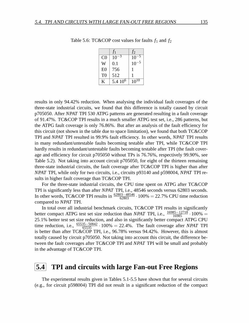
5.4. TPI AND CIRCUITS WITH LARGE FAN-OUT FREE REGIONS 135
Table 5.6: TC&COP cost values for faults f1 and f2
f1 f2
C0 10−3 10−5
W 0.1 10−5
E0 756 1T0 512 1K 5.4 106 1010
results in only 94.42% reduction. When analysing the individual fault coverages of thethree-state industrial circuits, we found that this difference is totally caused by circuitp705050. After NPAT TPI 530 ATPG patterns are generated resulting in a fault coverageof 91.47%. TC&COP TPI results in a much smaller ATPG test set, i.e., 286 patterns, butthe ATPG fault coverage is only 76.86%. But after an analysis of the fault efficiency forthis circuit (not shown in the table due to space limitation), we found that both TC&COPTPI and NPAT TPI resulted in 99.9% fault efficiency. In other words, NPAT TPI resultsin many redundant/untestable faults becoming testable after TPI, while TC&COP TPIhardly results in redundant/untestable faults becoming testable after TPI (the fault cover-age and efficiency for circuit p705050 without TPs is 76.76%, respectively 99.90%, seeTable 5.2). Not taking into account circuit p705050, for eight of the thirteen remainingthree-state industrial circuits, the fault coverage after TC&COP TPI is higher than afterNPAT TPI, while only for two circuits, i.e., circuits p93140 and p598004, NPAT TPI re-sults in higher fault coverage than TC&COP TPI.
For the three-state industrial circuits, the CPU time spent on ATPG after TC&COPTPI is significantly less than after NPAT TPI, i.e., 48546 seconds versus 62803 seconds.In other words, TC&COP TPI results in 62803−48546
62803 ·100% = 22.7% CPU time reductioncompared to NPAT TPI.
In total over all industrial benchmark circuits, TC&COP TPI results in significantlybetter compact ATPG test set size reduction than NPAT TPI, i.e., 16985−12718
16985 · 100% =25.1% better test set size reduction, and also in significantly better compact ATPG CPUtime reduction, i.e., 65535−50842
65535 · 100% = 22.4%. The fault coverage after NPAT TPIis better than after TC&COP TPI, i.e., 96.78% versus 94.42%. However, this is almosttotally caused by circuit p705050. Not taking into account this circuit, the difference be-tween the fault coverages after TC&COP TPI and NPAT TPI will be small and probablyin the advantage of TC&COP TPI.
5.4 TPI and circuits with large Fan-out Free Regions
The experimental results given in Tables 5.1-5.5 have shown that for several circuits(e.g., for circuit p598004) TPI did not result in a significant reduction of the compact
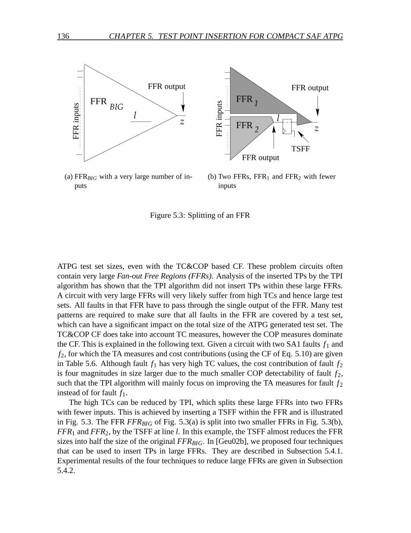
136 CHAPTER 5. TEST POINT INSERTION FOR COMPACT SAF ATPG
z
FFR
FFR outputFF
R in
puts
lBIG
(a) FFRBIG with a very large number of in-puts
z
FFR output
FFR output
FFR
inpu
ts
FFR
TSFF
2
1
l
FFR
(b) Two FFRs, FFR1 and FFR2 with fewerinputs
Figure 5.3: Splitting of an FFR
ATPG test set sizes, even with the TC&COP based CF. These problem circuits oftencontain very large Fan-out Free Regions (FFRs). Analysis of the inserted TPs by the TPIalgorithm has shown that the TPI algorithm did not insert TPs within these large FFRs.A circuit with very large FFRs will very likely suffer from high TCs and hence large testsets. All faults in that FFR have to pass through the single output of the FFR. Many testpatterns are required to make sure that all faults in the FFR are covered by a test set,which can have a significant impact on the total size of the ATPG generated test set. TheTC&COP CF does take into account TC measures, however the COP measures dominatethe CF. This is explained in the following text. Given a circuit with two SA1 faults f1 andf2, for which the TA measures and cost contributions (using the CF of Eq. 5.10) are givenin Table 5.6. Although fault f1 has very high TC values, the cost contribution of fault f2
is four magnitudes in size larger due to the much smaller COP detectability of fault f2,such that the TPI algorithm will mainly focus on improving the TA measures for fault f2
instead of for fault f1.The high TCs can be reduced by TPI, which splits these large FFRs into two FFRs
with fewer inputs. This is achieved by inserting a TSFF within the FFR and is illustratedin Fig. 5.3. The FFR FFRBIG of Fig. 5.3(a) is split into two smaller FFRs in Fig. 5.3(b),FFR1 and FFR2, by the TSFF at line l. In this example, the TSFF almost reduces the FFRsizes into half the size of the original FFRBIG. In [Geu02b], we proposed four techniquesthat can be used to insert TPs in large FFRs. They are described in Subsection 5.4.1.Experimental results of the four techniques to reduce large FFRs are given in Subsection5.4.2.
5.4. TPI AND CIRCUITS WITH LARGE FAN-OUT FREE REGIONS 137
5.4.1 Four TPI techniques for reducing large FFRs
The TPI for ATPG algorithm is extended with a TPI pre-process for reducing verylarge FFRs in the circuit. This pre-process should be run before normal TPI using theHybrid TPI algorithm (with the TC&COP CF). While the Hybrid CRF TPI algorithm isa global optimization TPI method, the TPI pre-process for reducing large FFRs will be alocal optimization method. Only the large FFR testability problem is targeted. The TPIpre-process searches for very large FFRs in the circuit and insert TPs in the large FFRs toreduce them. In the following text four techniques are described that can be used to findand split the FFRs. The size of an FFR corresponds to the number of inputs of the FFR.
The first question which has to be answered is the definition of a ’large FFR’. We usetwo definitions for a large FFR:
A: An FFR is large when it has more than LARGE_FFR_THRESHOLD inputs.LARGE_FFR_THRESHOLD is a user-defined threshold.
B: An FFR is large when it has more than FFR + 3*σFFR inputs. FFR is the averagesize of an FFR in the circuit and σFFR is the standard deviation of the FFR sizedistribution. Because most of the FFRs only have a small number of inputs, FFRand σFFR are only determined for the larger FFRs (≥ 10 inputs).
Definition A uses a fixed, user-defined threshold to determine whether an FFR is verylarge or not, while definition B uses statistics to determine if an FFR is too large.
As already described, large FFRs usually have high TCs. This has led to two strategiesto reduce the FFR sizes:
1: The TP candidate that splits the FFR into two smaller FFRs of which the number ofinputs are closest to each other (i.e., two approximately equal sized FFRs), is theTP that will be inserted in the FFR.
2: The TP candidate that splits the FFR into two smaller FFRs with both the lowest TCvalues, is the TP that will be inserted.
The two definitions of large FFRs and the two strategies are combined into four tech-niques to reduce large FFRs, i.e., methods
A1: A TP will be inserted in the largest FFR, with at least LARGE_FFR_THRESHOLD inputs,that results in two smaller (approximately) equal sized FFRs.
A2: A TP will be inserted in the largest FFR, with at least LARGE_FFR_THRESHOLD inputs,that results in two smaller FFRs with both the lowest TC values.
B1: A TP will be inserted in the largest, with at least FFR + 3*σFFR inputs, that resultsin two smaller (approximately) equal sized FFRs.
B2: A TP will be inserted in the largest, with at least FFR + 3*σFFR inputs, that resultsin two smaller FFRs with both the lowest TC values.
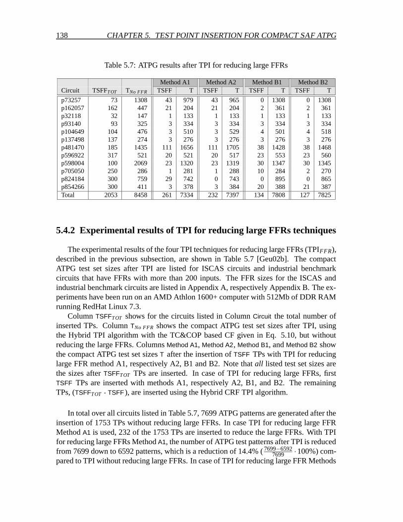
138 CHAPTER 5. TEST POINT INSERTION FOR COMPACT SAF ATPG
Table 5.7: ATPG results after TPI for reducing large FFRs
Method A1 Method A2 Method B1 Method B2Circuit TSFFTOT TNo FFR TSFF T TSFF T TSFF T TSFF T
p73257 73 1308 43 979 43 965 0 1308 0 1308p162057 162 447 21 204 21 204 2 361 2 361p32118 32 147 1 133 1 133 1 133 1 133p93140 93 325 3 334 3 334 3 334 3 334p104649 104 476 3 510 3 529 4 501 4 518p137498 137 274 3 276 3 276 3 276 3 276p481470 185 1435 111 1656 111 1705 38 1428 38 1468p596922 317 521 20 521 20 517 23 553 23 560p598004 100 2069 23 1320 23 1319 30 1347 30 1345p705050 250 286 1 281 1 288 10 284 2 270p824184 300 759 29 742 0 743 0 895 0 865p854266 300 411 3 378 3 384 20 388 21 387Total 2053 8458 261 7334 232 7397 134 7808 127 7825
5.4.2 Experimental results of TPI for reducing large FFRs techniques
The experimental results of the four TPI techniques for reducing large FFRs (TPIFFR),described in the previous subsection, are shown in Table 5.7 [Geu02b]. The compactATPG test set sizes after TPI are listed for ISCAS circuits and industrial benchmarkcircuits that have FFRs with more than 200 inputs. The FFR sizes for the ISCAS andindustrial benchmark circuits are listed in Appendix A, respectively Appendix B. The ex-periments have been run on an AMD Athlon 1600+ computer with 512Mb of DDR RAMrunning RedHat Linux 7.3.
Column TSFFTOT shows for the circuits listed in Column Circuit the total number ofinserted TPs. Column TNo FFR shows the compact ATPG test set sizes after TPI, usingthe Hybrid TPI algorithm with the TC&COP based CF given in Eq. 5.10, but withoutreducing the large FFRs. Columns Method A1, Method A2, Method B1, and Method B2 showthe compact ATPG test set sizes T after the insertion of TSFF TPs with TPI for reducinglarge FFR method A1, respectively A2, B1 and B2. Note that all listed test set sizes arethe sizes after TSFFTOT TPs are inserted. In case of TPI for reducing large FFRs, firstTSFF TPs are inserted with methods A1, respectively A2, B1, and B2. The remainingTPs, (TSFFTOT - TSFF ), are inserted using the Hybrid CRF TPI algorithm.
In total over all circuits listed in Table 5.7, 7699 ATPG patterns are generated after theinsertion of 1753 TPs without reducing large FFRs. In case TPI for reducing large FFRMethod A1 is used, 232 of the 1753 TPs are inserted to reduce the large FFRs. With TPIfor reducing large FFRs Method A1, the number of ATPG test patterns after TPI is reducedfrom 7699 down to 6592 patterns, which is a reduction of 14.4% ( 7699−6592
7699 ·100%) com-pared to TPI without reducing large FFRs. In case of TPI for reducing large FFR Methods

5.4. TPI AND CIRCUITS WITH LARGE FAN-OUT FREE REGIONS 139
A2, B1, and B2, the number of ATPG patterns after TPI is reduced from 7699 to 6654patterns (13.6% reduction compared to TPI without reducing large FFRs) for MethodA2, respectively to 6913 patterns (10.2% reduction) for Method B1, and to 6960 patterns(9.6% reduction) for Method B2. Overall, Method A1 results in the best test set size re-duction.
From these results one can conclude that using definition A for a large FFR results inbetter test set size reduction than definition B; Methods A1 and A2, which are based ondefinition A, have better test set size reduction than Methods B1 and B2, which are basedon definition B. These differences in reduction are mainly caused by the large differencein test set size reduction for circuit p73257. This circuit contains over 50 FFRs with morethan 200 inputs and because of this, FFR + 3 ·σFFR is larger than 269 (the largest FFR)and no TPs are inserted by TPI for reducing large FFRs methods B1 and B2. Although thiscircuit only contains semi-large FFRs, it does suffer from a large test set and the resultsof TPI for reducing large FFR methods Al and A2 show that TPI for reducing large FFRsresults in significantly better test set size reduction.
In contrast to the results of NPAT TPI and TC&COP TPI shown in Table 5.5, the re-sults in Table 5.7 show that it is possible to achieve significant compact ATPG test set sizereduction for circuit p598004, as long as TPI for reducing large FFRs is used. With TPIfor reducing large FFRs, the ATPG test set size for this circuit is reduced to 1320-1345patterns which is considerably less than the 2129 patterns without TPI.
The experimental results in [Geu02b] showed that far more TPs were inserted withMethods B than with Methods A. The results in Table 5.7 show that fewer TPs are insertedwith Methods B than with Methods A. Due to a bug in the TPI tool, the FFR+3 ·σFFR wasnot set correctly in [Geu02b]; as a result far too many TPs were inserted with Methods B
in [Geu02b] for the larger circuits. Inserting more TPs with a TPI for reducing large FFRmethod does not always result in a better test set size reduction. For circuit p481470 moreTPs are inserted with Methods A than with Methods B, but the test set size reduction forMethods B are better than for Methods A; i.e., 1428-1468 patterns for Methods B versus1657-1705 patterns for Methods A. Too many TPs in circuit p481470 are inserted withthe TPI for reducing large FFR Methods A, i.e., 111 out of 185, such that only a smallnumber of TPs are inserted with the Hybrid TPI algorithm. More TPs with the Hybrid TPIalgorithm are probably required for this circuit to solve the ATPG testability problems inthis circuit, other testability problems than large FFRs.
Method A1 results in better test set size reduction than Method A2, with the same num-ber of TPs inserted for reducing large FFRs. Also Method B1 results in better test set sizereduction than Method B2. Given these results, it can be concluded that using Strategy 1
to reduce large FFRs results in better test set size reduction than Strategy 2. More equallysized FFRs seems more important for the ATPG tool than better test counts reduction.
Overall, the results in Table 5.7 show that by using TPI for reducing large FFR meth-ods for circuits with large FFRs, an extra ATPG test set size reduction of 9.6% to 14.4%can be obtained. Method A1 results in the best test set size reduction. In the remaining partof this dissertation, TPI for reducing large FFR method A1 is used as a TPI pre-process

140 CHAPTER 5. TEST POINT INSERTION FOR COMPACT SAF ATPG
of the Hybrid TPI algorithm.
5.5 Multi-stage TPI with dynamic cost function selection
Every circuit has its own characteristics and therefore also its own testability prob-lems. Some circuits suffer from many RPR faults, while other circuits suffer from signallines with high TCs, as described in Section 5.3. It is also possible that the circuit suffersfrom a combination of testability problems. The Hybrid CRF TPI algorithm for industrialcircuits uses a CF to determine where in the circuit TPs should be inserted. It is importantthat a CF is used that takes into account the TA measures for the testability problems thatreally exist in the circuit. E.g., using a TC based CF, while the circuit does not suffer fromhigh TCs, does not seem to be useful.
In [Geu02b] we proposed a TPI pre-process that selects a CF for the Hybrid TPI al-gorithm for industrial circuits that tries to solve the hardest test problem that is found inthe circuit. The TA measures, extracted from the circuit, are analyzed to identify thesetest problems. Instead of inserting all TPs using the selected CF, we proposed to split theTPI process into multiple stages. In each stage, the TPI pre-process is run to select thebest CF given the TA measures of the current circuit (including already inserted TPs fromprevious stages). Several TPs are inserted by the TPI algorithm using this CF. In the nextstage, the TPI pre-process is run again to select a new cost function.
The CF selection procedure introduced in [Geu02b] is described in Subsection 5.5.1and the corresponding experimental results are shown in Subsection 5.5.2.
5.5.1 The cost function selection procedure
COP, SCOAP and TC give, for each line, measures for different possible testabilityproblems in the circuit; i.e., COP gives measures for the PR detectability, SCOAP for thenumber of necessary input assignments and TC for the number of tests that have to prop-agate through a line. The TPI pre-process analyzes the TA measures to find out whetherthey indicate that there are testability problems. During the analysis, priorities are as-signed on improving the COP, SCOAP and TC measures. The higher the priority for aTA measure, the higher the testability problem corresponding to this TA measure and themore important it becomes to improve these TA measures. For the different TA measures,the following priority schemes are used:COP priority:
The COP priority is determined by the number of faults with a COP detectability(Pd f ) below a given threshold value. The more faults with a Pd f below this threshold, thehigher the priority. The priority is also higher, when there are faults with very low Pd f s,e.g., below 1−10, to make sure that the TPI algorithm will target these very hard-to-testfaults, even when there are only a few of them.SCOAP priority:
5.5. MULTI-STAGE TPI WITH DYNAMIC COST FUNCTION SELECTION 141
The SCOAP priority is determined in a similar way as the COP priority. The numberof faults with SCOAP values higher than a given threshold determine the priority. Asmentioned in Subsection 5.2.1, relative SCOAP values (SCOAP values of a given signalline compared to SCOAP values of other lines) are more useful than absolute SCOAPvalues. Therefore the threshold is determined by the distribution of the SCOAP valuesand is set at SCOAP + 3 ·σSCOAP (standard deviation). This threshold equation has beenchosen experimentally.TC priority:
For the TC only two priority values are used, 0 and 1. Experiments with more prior-ity values have not taken place. Again a given threshold is used to differentiate betweenthese priorities. When there are TC values (T 0+T 1) for lines higher than this threshold,the priority is 1, otherwise 0. This threshold has experimentally been set at 40.
When the COP priority is higher than the SCOAP priority, a COP-based CF is se-lected. On the other hand, when the SCOAP priority is higher, a SCOAP based CF isselected. When COP and SCOAP have an equally high priority, a CF is selected thattakes into account both COP and SCOAP. The selected CF will also take into accountTCs when the TC priority is 1.
Two kinds of COP CFs have been described in this dissertation, the original COPbased CF of Tsai et al. [Tsa97]: 1
Pd f, from now on called “Tsai CF”, and our proposed
NPAT CF: (1−Pd f )NPAT . The CF selection procedure also has to select which kind will
be used in the selected CF. Subsection 4.3.3 already described that the Tsai CF mainly fo-cuses on improving the detection probability of the hardest RPR fault(s), while the NPATCF focuses on improving the detection probabilities of all faults with low detection prob-abilities. These faults will have a cost contribution of (nearly) 1. Several properties of theNPAT CF are described in the following text in order to explain how to choose betweenthe Tsai and the NPAT CF and how to select the NPAT value.
The NPAT CF divides the faults in the circuit into three groups:
Group 1: The faults with a cost contribution of (almost) 1.
Group 2: The faults with a cost contribution of (almost) 0.
Group 3: The faults with a cost contribution larger than 0 but smaller than 1.
Whether a fault belongs to Group 1, 2 or 3 depends both on its detection probability andon the value of NPAT . This is illustrated in Fig. 5.4. The detection probabilities of theSA0 faults for the first 1000 signal lines in circuit s15850.1 are shown. Fig. 5.4(a) showsthe different fault groups in case NPAT =320. COST=1 represents the group with a costcontribution of almost 1 (>0.95), COST=0 the group with a cost contribution of almost 0(<0.05) and 0<COST<1 the group with a cost contribution between 0.05 and 0.95.

142 CHAPTER 5. TEST POINT INSERTION FOR COMPACT SAF ATPG
Detection probabilities in circuit s15850.1
cost=1
0<cost<1
1e−12
1e−10
1e−08
1e−06
0.01
1
0 200 400 600 800 1000
0.0001
Det
ectio
n pr
obab
ility
Signal line
cost=0
stuck−at 0 faults
(a) Cost contributions for NPAT =320
Detection probabilities in circuit s15850.1
cost=1
0<cost<1
1e−12
1e−10
1e−08
1e−06
0.01
1
0 200 400 600 800 1000
0.0001
Det
ectio
n pr
obab
ility
Signal line
cost=0
stuck−at 0 faults
(b) Cost contributions for NPAT =320000
Figure 5.4: Impact of NPAT on the cost contributions of faults in circuit s15850.1
The Hybrid TPI algorithm targets at reducing the global cost of the circuit. The algo-rithm tries to improve detection probabilities of faults in the circuit that results in a costcontribution reduction from non-zero (�0) to (almost) 0, hence the TPI algorithm targetsthe faults in Group 1, and partially the faults in Group 2. But when NPAT is low, thereare a lot of faults in Groups 1 and 2. Given Fig. 5.4(a) with NPAT =320, it is possible thatthe TPI algorithm insert TPs that improve the detection probabilities of lots of faults withdetection probabilities between 10−3 and 10−4, while it does not improve the detectionprobabilities of the really hard-to-test faults, i.e., faults with detection probabilities below10−7.
When NPAT is increased to 320000, shown in Fig. 5.4(b), the faults with detectionprobabilities between 10−3 and 10−4 have a cost contribution of (almost) 0 and the TPIalgorithm will not target these faults. Now the TPI algorithm will mainly target on thehard-to-test faults, the faults with a detection probability lower than 10−7.
In case the cost selection procedure selects the NPAT CF as COP based CF, the NPATparameter will be selected such that approximately 5% of the faults will be in Groups 1and 2. The TPI algorithm will mainly focus on improving the detection probability of the5% hardest-to-test faults and will not be influenced by the less hard-to-test faults.
At this point still the question has to be answered when to use the Tsai COP CF andwhen to use the NPAT CF. In case there are very low detection probabilities in the circuit,often the difference in detection probabilities within the 5% lowest detection probabilitiesis high, i.e., many orders (>5) of magnitude. In that case it is still possible that althougha TP might improve the detection probability of a fault with several orders of magnitude,its NPAT cost contribution hardly changes and stays almost 1. This is illustrated in Fig.
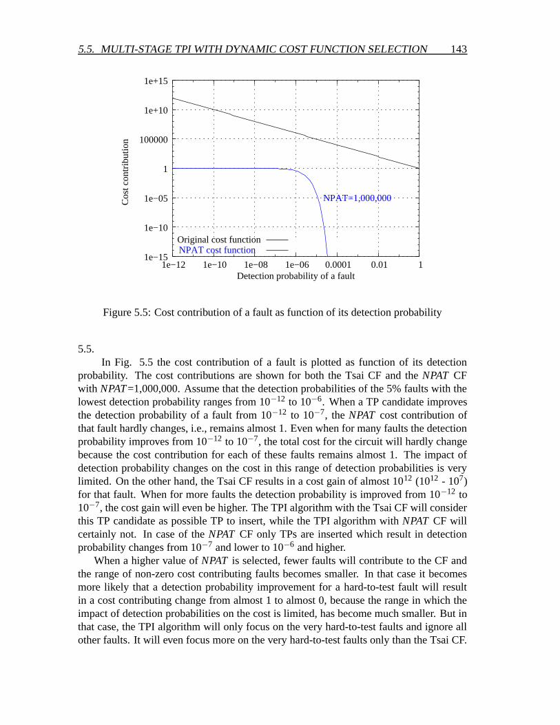
5.5. MULTI-STAGE TPI WITH DYNAMIC COST FUNCTION SELECTION 143
NPAT=1,000,000
1e−15
1e−10
1e−05
1
100000
1e+10
1e+15
1e−12 1e−10 1e−08 1e−06 0.0001 0.01 1
Cos
t con
trib
utio
n
Detection probability of a fault
Original cost functionNPAT cost function
Figure 5.5: Cost contribution of a fault as function of its detection probability
5.5.In Fig. 5.5 the cost contribution of a fault is plotted as function of its detection
probability. The cost contributions are shown for both the Tsai CF and the NPAT CFwith NPAT =1,000,000. Assume that the detection probabilities of the 5% faults with thelowest detection probability ranges from 10−12 to 10−6. When a TP candidate improvesthe detection probability of a fault from 10−12 to 10−7, the NPAT cost contribution ofthat fault hardly changes, i.e., remains almost 1. Even when for many faults the detectionprobability improves from 10−12 to 10−7, the total cost for the circuit will hardly changebecause the cost contribution for each of these faults remains almost 1. The impact ofdetection probability changes on the cost in this range of detection probabilities is verylimited. On the other hand, the Tsai CF results in a cost gain of almost 1012 (1012 - 107)for that fault. When for more faults the detection probability is improved from 10−12 to10−7, the cost gain will even be higher. The TPI algorithm with the Tsai CF will considerthis TP candidate as possible TP to insert, while the TPI algorithm with NPAT CF willcertainly not. In case of the NPAT CF only TPs are inserted which result in detectionprobability changes from 10−7 and lower to 10−6 and higher.
When a higher value of NPAT is selected, fewer faults will contribute to the CF andthe range of non-zero cost contributing faults becomes smaller. In that case it becomesmore likely that a detection probability improvement for a hard-to-test fault will resultin a cost contributing change from almost 1 to almost 0, because the range in which theimpact of detection probabilities on the cost is limited, has become much smaller. But inthat case, the TPI algorithm will only focus on the very hard-to-test faults and ignore allother faults. It will even focus more on the very hard-to-test faults only than the Tsai CF.
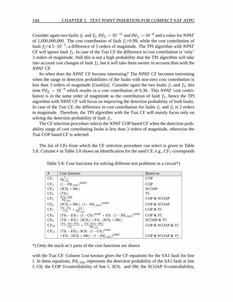
144 CHAPTER 5. TEST POINT INSERTION FOR COMPACT SAF ATPG
Consider again two faults f1 and f2, Pd f1 = 10−11 and Pd f1 = 10−8 and a value for NPATof 1,000,000,000. The cost contribution of fault f1=0.99, while the cost contribution offault f2=4.5 ·10−5, a difference of 5 orders of magnitude. The TPI algorithm with NPATCF will ignore fault f2. In case of the Tsai CF the difference in cost contribution is ’only’3 orders of magnitude. Still this is not a high probability that the TPI algorithm will takeinto account cost changes of fault f2, but it will take them sooner in account than with theNPAT CF.
So when does the NPAT CF become interesting? The NPAT CF becomes interestingwhen the range in detection probabilities of the faults with non-zero cost contribution isless than 3 orders of magnitude [Geu02a]. Consider again the two faults f1 and f2, thistime Pd f2 = 10−9 which results in a cost contribution of 0.36. This NPAT cost contri-bution is in the same order of magnitude as the contribution of fault f1, hence the TPIalgorithm with NPAT CF will focus on improving the detection probability of both faults.In case of the Tsai CF, the difference in cost contribution for faults f1 and f2 is 2 ordersin magnitude. Therefore, the TPI algorithm with the Tsai CF will mainly focus only onsolving the detection probability of fault f1.
The CF selection procedure selects the NPAT COP based CF when the detection prob-ability range of cost contributing faults is less than 3 orders of magnitude, otherwise theTsai COP based CF is selected.
The list of CFs from which the CF selection procedure can select is given in Table5.8. Column # in Table 5.8 shows an identification for the used CF, e.g., CF1 corresponds
Table 5.8: Cost functions for solving different test problems in a circuit*)
# Cost function Based onCF1
1Pdl/SA1
COP
CF2 (1−Pdl/SA1)NPAT COP
CF3 (SC0l +SWl) SCOAPCF4 (T 0l) TCCF5
SC0l+SWlPdl/SA1
COP & SCOAP
CF6 (SC0l +SWl) · (1−Pdl/SA1)NPAT COP & SCOAP
CF7T 0l−E0l
C0l+ E0
Pdl/SA1COP & TC
CF8 (T 0l −E0l) · (1−C0l)NPAT +E0l · (1−Pdl/SA1)
NPAT COP & TCCF9 (T 0l −E0l) · (SC0l)+E0l · (SC0l +SWl) SCOAP & TC
CF10(T 0l−E0l)·SC0l
C0l+ E0l ·(SC0l+SWl)
Pdl/SA1COP & SCOAP & TC
CF11 (T 0l −E0l) ·SC0l · (1−C0l)NPAT
+E0l · (SC0l +SWl) · (1−Pdl/SA1)NPAT COP & SCOAP & TC
*) Only the stuck-at 1 parts of the cost functions are shown
with the Tsai CF. Column Cost function gives the CF equations for the SA1 fault for linel. In these equations, Pdl/SA1 represents the detection probability of the SA1 fault at linel, C0l the COP 0-controllability of line l, SC0l and SWl the SCOAP 0-controllability,

5.5. MULTI-STAGE TPI WITH DYNAMIC COST FUNCTION SELECTION 145
respectively SCOAP observability of line l, E0l and T 0l the essential-zeros, respectivelytotal-zeros counts for line l. Only the part of the CF with respect to the SA1 fault isshown in order to limit the size of the table. Finally, Column Based on shows on whichTA measures this CF is based. Given that there are two possible COP-based CFs, thereare 11 possible CFs: two COP-only, one SCOAP-only, one TC-only, two COP&SCOAP,two COP&TC, one SCOAP&TC, and two COP&SCOAP&TC based CFs.
5.5.2 Experimental results of multi-stage TPI
This subsection shows the impact of multi-stage TPI, with the TPI pre-process that se-lects the CF, on the compact ATPG test set sizes. The results of multi-stage TPI [Geu02b]are compared with the results of the COP&TC based CF proposed in Section 5.3. Thecomparison results are given in Tables 5.9 and 5.10 for the ISCAS respectively industrialcircuits. Multi-stage TPI includes the TPI pre-process for reducing large FFRs [Geu02b]as described in Section 5.4.
Column TC&COP TPI shows the compact ATPG results for the circuits listed in Col-umn Circuit after TC&COP TPI; the ATPG test set size (T ), the ATPG fault coverage(FC(%)) and the CPU time spent on ATPG (CPU) are listed. Column TPI shows the num-ber of inserted TSFF TPs (TSFF ) and the CPU time spent on multi-stage TPI (CPU).Column multi-stage TPI shows the compact ATPG results for the circuit when multi-stageTPI has been used; the ATPG test set size (T ), the ATPG fault coverage (FC(%)) and theCPU time spent on ATPG (CPU) after multi-stage TPI are listed.
The compact ATPG results, listed in Table 5.9, show that with multi-stage TPI 48fewer ATPG patterns are generated than with TC&COP TPI, i.e., 1014 patterns are gen-erated after multi-stage TPI versus 1062 patterns after TC&COP TPI. In other words,multi-stage TPI results in 4.5% extra test set size reduction compared to TC&COP TPI.For all three sets of ISCAS circuits, i.e., ISCAS’85, ISCAS’89 and ISCAS’89 addendum,better test set size reduction is achieved with multi-stage TPI. However, there are threecircuits for which the test set size reduction is not as good as with TC&COP TPI, i.e.,circuits s9234.1, s13207.1 and s938a. For these circuits, the multi-stage TPI does notselect the best CF, although still very good test set size reduction has been achieved afterTPI compared to the results without TPI, see Appendix A. On the other hand, the numberof compact ATPG test patterns for circuits c7552, s15850.1 and s38584.1 is considerablysmaller with multi-stage TPI compared to TC&COP TP. For these circuits it is clearlyshown that the multi-stage TPI results in better ATPG testability improvement.
The ATPG fault coverages of the ISCAS circuits after TC&COP TPI and multi-stageTPI do not differ a lot, i.e., 0.01% (99.02%-99.01%) for the ISCAS’85 circuits, 0.16% forthe ISCAS’89 circuits, and 0.13% over all ISCAS circuits. For all sets of ISCAS circuits,multi-stage TPI results in the better fault coverage.
Also the ATPG CPU times do not differ a lot. Overall, the ATPG CPU times for the

146 CHAPTER 5. TEST POINT INSERTION FOR COMPACT SAF ATPG
Table 5.9: Compact ATPG results of ISCAS circuits after multi-stage TPI
TC&COP TPI TPI multi-stage TPICircuit T FC(%) CPU TSFF CPU T FC(%) CPU
c1908 42 99.92 0.46 s 25 1.25 s 40 99.92 0.45 sc3540 73 97.67 1.69 s 25 4.45 s 70 97.73 2.26 sc7552 74 99.40 3.40 s 40 7.58 s 56 99.40 3.01 sSubtotal 189 99.01 5.55 s 90 13.3 s 166 99.02 5.73 ss1196 52 100.00 0.30 s 20 0.65 s 52 100.00 0.31 ss1488 88 100.00 0.44 s 20 0.91 s 81 100.00 0.47 ss1494 87 99.87 0.46 s 20 0.92 s 82 99.93 0.45 ss5378 60 98.91 1.53 s 30 2.60 s 58 98.98 1.62 ss9234.1 51 94.69 4.24 s 50 8.49 s 57 94.60 4.65 ss13207.1 202 99.16 11.0 s 50 12.8 s 212 99.15 11.5 ss15850.1 88 98.38 9.72 s 50 13.2 s 75 98.36 8.75 ss38584.1 110 96.53 36.4 s 50 34.9 s 98 96.91 34.4 sSubtotal 738 97.39 64.0 s 290 74.4 s 715 97.55 62.2 ss499a 28 100.00 0.18 s 8 0.21 s 28 100.00 0.18 ss938a 40 100.00 0.25 s 12 0.44 s 41 100.00 0.25 ss3330a 67 100.00 1.03 s 32 1.89 s 64 100.00 1.06 sSubtotal 135 100.00 1.46 s 52 2.54 s 133 100.00 1.48 s
Total 1062 97.71 71.1 s 432 90.2 s 1014 97.84 69.4 s
ISCAS circuits after multi-stage TPI are 1.7 seconds less than after TC&COP TPI (69.4seconds for multi-stage TPI versus 71.1 seconds for TC&COP TPI).
The results of the industrial benchmark circuits, listed in Table 5.10, also show thatmulti-stage TPI results in significantly better compact ATPG test set size reduction thanTC&COP TPI. For the Boolean industrial circuits, the ATPG test set size is reduced from4200 patterns with TC&COP TPI to 3050 patterns with multi-stage TPI. This meansthat with multi-stage TPI a test set size reduction of 4200−3050
4200 · 100% = 27.4% has beenachieved compared to TC&COP TPI. Especially for circuits p73257 and p162057, bettertest set size reduction has been achieved. In case of circuit p162057, this better reduc-tion is totally the result of the usage of the TPI for reducing large FFRs pre-process inmulti-stage TPI, see Table 5.7. In case of circuit p73257, this is only partially true. Aftermulti-stage TPI on circuit p73257, the ATPG test set size contains 413 patterns less (566patterns versus 979 patterns) than with TPI for reducing large FFR method A1 in combi-nation with TC&COP TPI, see Table 5.7. Compared to TC&COP TPI without reducinglarge FFRs, multi-stage TPI on circuit p73257 results even in 56.7% ( 1308−566
1308 · 100%)extra test set size reduction.
The fault coverage differences between TC&COP TPI and multi-stage TPI for the

5.5. MULTI-STAGE TPI WITH DYNAMIC COST FUNCTION SELECTION 147
Table 5.10: Compact ATPG results of industrial circuits after multi-stage TPI
TC&COP TPI TPI multi-stage TPICircuit T FC(%) CPU TSFF CPU T FC(%) CPU
p7653 178 99.62 8.74 s 15 6.91 s 158 99.63 8.66 sp14148 260 99.99 19.9 s 15 5.68 s 212 99.99 17.3 sp27811 97 95.22 25.2 s 38 16.0 s 87 95.22 25.6 sp31025 463 98.87 129 s 25 30.9 s 445 98.74 122 sp34592 198 99.98 75.4 s 34 22.1 s 173 99.97 70.1 sp36503 159 97.25 48.1 s 30 23.5 s 125 97.25 42.2 sp43282 197 97.73 127 s 49 49.9 s 183 97.79 118 sp43663 132 99.25 40.1 s 50 28.5 s 115 99.26 38.9 sp72767 302 97.25 404 s 50 147 s 304 97.41 400 sp73133 285 97.39 404 s 50 164 s 270 97.30 393 sp73257 1308 98.09 561 s 73 133 s 566 98.25 356 sp75344 174 99.31 102 s 55 70.4 s 182 99.33 109 sp162057 447 98.69 348 s 162 627 s 230 98.79 273 sSubtotal 4200 98.28 2296 s 646 1326 s 3050 98.32 1977 sp32118 147 93.56 30.2 s 32 20.0 s 134 93.57 30.7 sp37021 176 77.28 23.2 s 37 25.3 s 208 77.23 24.0 sp66171 1177 96.79 354 s 66 379 s 1138 96.79 348 sp71553 96 96.86 290 s 71 145 s 87 96.78 228 sp93140 325 94.03 587 s 93 173 s 386 94.03 614 sp104649 476 99.39 367 s 104 191 s 480 99.39 346 sp114605 366 99.01 500 s 80 173 s 381 98.94 526 sp137498 274 98.86 177 s 137 308 s 298 98.85 200 sp481470 1435 99.28 8390 s 185 904 s 1693 99.26 11283 sp596922 521 96.97 2595 s 317 2894 s 450 96.95 2953 sp598004 2069 98.74 4313 s 100 932 s 1440 98.74 4022 sp705050 286 76.86 6817 s 250 2653 s 256 76.86 6568 sp824184 759 96.73 18655 s 300 3952 s 749 96.74 18123 sp854266 411 97.65 5442 s 300 3911 s 414 97.68 6136 sSubtotal 8518 94.42 48546 s 2072 16666 s 8114 94.42 51406 s
Total 12718 94.92 50842 s 2718 17992 s 11164 94.92 53384 s
Boolean industrial circuits are very limited, 98.28% after TC&COP TPI versus 98.32%after multi-stage TPI. For seven of the thirteen Boolean industrial circuits, multi-stageTPI results in the better fault coverage, while TC&COP TPI only results three times inthe better fault coverage.
The compact ATPG CPU times after multi-stage TPI are also less than the compactATPG CPU times after TC&COP TPI; 1977 seconds versus 2296 seconds. In other words,multi-stage TPI results in 2296−1977
2296 · 100% = 13.9% extra ATPG CPU time reduction

148 CHAPTER 5. TEST POINT INSERTION FOR COMPACT SAF ATPG
compared to TC&COP TPI. Again this difference is mainly caused by circuits p73257and p162057. For the ATPG tool it becomes much easier to activate faults or propagatefault effects when there are fewer large FFRs with high TCs.
The compact ATPG test set size reduction after multi-stage TPI for the three-stateindustrial circuits is less compared to the reduction for the Boolean industrial circuits.8114 ATPG patterns are generated after multi-stage TPI compared to 8518 patterns af-ter TC&COP TPI; in other words a reduction of 8518−8114
8518 · 100% = 4.7%. A very largeamount of this difference is caused by the usage of TPI for reducing large FFRs withinmulti-stage TPI, see the results of circuits p481470 and p598004 in Tables 5.7 and 5.10.The multi-stage TPI algorithm is not able to find really better CFs for the three-state in-dustrial circuits compared to the TC&COP CF, i.e., CF7. The larger three-state industrialcircuits mainly suffer from poor COP detectability and high TC values, which is exactlywhat TC&COP TPI tries to improve.
The ATPG fault coverages after multi-stage TPI and TC&COP TPI are the same, i.e.,94.42%. Just like TC&COP TPI, multi-stage TPI is also not able to improve the faultcoverage for circuit p705050, which NPAT TPI was able to do (see Tables 5.2 and 5.5).For all three-state industrial circuits, the differences in ATPG fault coverages after TPI islimited to less than 0.1%.
Multi-stage TPI results in longer ATPG CPU times than TC&COP TPI for the three-state industrial circuits. This is mainly caused by circuit p481470. As explained in Sub-section 5.4.2, most of the inserted TPs in circuit p481470 are inserted by the TPI forreducing large FFR method A1 (included in multi-stage TPI), i.e., 111 out of 185 TPs.Only a relatively small number of TPs is inserted by the Hybrid CRF TPI method. Thiscircuit requires more TPs to be inserted with the Hybrid CRF TPI method in order toimprove other ATPG testability problems in the circuit, i.e., improve COP detectabilityand/or SCOAP observability.
Overall, the compact ATPG test set size reduction for the industrial benchmark circuitsis 12.2% better after multi-stage TPI compared to TC&COP TPI, i.e., 11164 patternsversus 12718 patterns. There is no significant difference in ATPG fault coverage betweenmulti-stage TPI and TC&COP TP; both result in 94.92% ATPG fault coverage. The CPUtime spent on ATPG is 5% more for multi-stage TPI compared to TC&COP TP TPI, i.e.,53384 seconds versus 48546 seconds. As explained above, this is mainly due to the manyTPs that are inserted in circuit p481470 for reducing large FFRs.
5.6 Summary and conclusions
The growth in ATPG test set sizes, caused by the increasing complexity of circuits,has a major impact on the ATE demands for the semiconductor industry. In this chap-ter it has been shown that TPI can be used to reduce the compact ATPG test set sizes,

5.6. SUMMARY AND CONCLUSIONS 149
hence reduce the ATE memory requirements and the long test time needed to apply thegenerated ATPG test sets. The TPI algorithm with the NPAT CF, which is only targetedon improving the PR testability of a circuit, is capable of significantly reducing compactATPG test set sizes.
For the set of ISCAS benchmark circuits, 43.5% test set size reduction has beenachieved, and for the industrial benchmark circuits, the test set size reduction was 26.1%.Besides reducing the ATPG test set sizes, NPAT TPI also resulted in an improvement ofthe ATPG fault coverage and a reduction of the CPU time spent on ATPG. For the ISCAScircuits, the ATPG fault coverage improved from 97% to 98%; this means that 33% of allfaults that were not covered by ATPG patterns before TPI, became detectable after NPATTPI. The ATPG CPU time spent on all ISCAS benchmark circuits has been reduced with31.8%.
For the industrial benchmark circuits, the ATPG fault coverage improved from 94.76%to 96.78%; in other words 40% of the faults that were not covered by ATPG patterns with-out TPI, became covered after NPAT TPI. The ATPG CPU time spent on the industrialcircuits has been reduced with 65.1%.
Although results show that, in general, significant test set size reductions can beachieved with NPAT TPI, there are however circuits for which the compact ATPG testset size reduction was not so high; i.e., less than 10%. These circuits suffer from othertestability problems that cause large test sets than only poor PR testability. We have pro-posed [Geu00] a CF for the Hybrid TPI algorithm for industrial circuits that not only takesinto account COP measures, but also test counts (TCs) [Hay74]. With TCs a lower boundon the compact ATPG test set size can be calculated. High TC measures indicate that theATPG test set size will also be high. Reducing the TCs may result in a reduction of theATPG test set size.
Experimental results on both the ISCAS benchmark and industrial circuits have shownthat the proposed TPI algorithm with the CF that takes TCs into account, i.e., TC&COPTPI, in general results in a better test set size reduction than NPAT TPI. Although forthe ISCAS benchmark circuits, only 1.7% extra test set size reduction is achieved, forthe industrial circuits 17% extra test set size reduction is achieved after TC&COP TPIcompared to NPAT TPI. The ISCAS circuits do not contain circuits that suffer from highTC values, while several industrial circuits do; this is the cause for the difference in extratest set size reduction between the ISCAS circuits and the industrial circuits.
Even with TC&COP TPI, there are still circuits for which the test set size reductionwas disappointing, e.g., for circuit p598004 less than 3% reduction had been achievedafter the insertion of 100 TPs with TC&COP TPI compared to the circuit without TPs.This circuit suffers from a very large FFR that results in very high TC values on the FFRoutput. Still, the TC&COP TPI (or NPAT TPI) algorithm did not insert TPs in this largeFFR. By extending the TPI algorithm with methods to reduce the sizes of large FFRs, alsosignificant test set size reduction can be achieved for circuits that suffer from very large

150 CHAPTER 5. TEST POINT INSERTION FOR COMPACT SAF ATPG
FFRs. Experimental results have shown that with these methods, also the test set size forcircuit p598004 can be reduced with 38%, from 2129 patterns down to 1320. Over the setof industrial benchmark circuits that contain large FFRs, 9.6% up to 14.4% extra test setsize reduction has been achieved when the TPI algorithm includes a TPI pre-process thatreduces the large FFRs by means of one of the TPI for reducing large FFR methods.
The ISCAS circuits do not suffer from high TCs; using a TC-based CF like in TC&COPTPI does not seem useful for these circuits. In general each circuit suffers from differ-ent testability problems. In this chapter we have proposed to use a TPI pre-process, thatanalyzes the TA measures of the circuit, to select a CF aimed at solving the testabilityproblems of that specific circuit. The TPI process is divided into multiple-stages. Beforeeach stage, the TPI pre-process is run to select the CF that targets the worst testabilityproblems in the circuit. Several TPs are inserted with that CF, after which the pre-processis run again to select a new CF. Because the inserted TPs improve the testability problemsin the circuit, another CF may become better to target the testability problems that existafter the currently inserted TPs. In this chapter we have shown that by dividing the TPIprocess into multiple stages, in order to select in each state a CF after an analysis of theTA measures, even better test set size reductions are achieved than using a COP-only (i.e.,NPAT ) CF or the TC&COP CF during the whole TPI process.
Experimental results of the proposed multi-stage TPI method, i.e., multi-stage TPI,show that for the ISCAS circuits the number of ATPG patterns is reduced with 4.5% com-pared to TC&COP TPI. For the industrial circuits, the extra reduction is 12.2% comparedto TC&COP TPI. Especially the reduction for the Boolean industrial circuits is large, i.e.,27.4%. The reduction for the three-state industrial circuits is 4.7%.
Comparing the compact ATPG results of multi-stage TPI with the ATPG results ofthe circuits without TPs, for the ISCAS circuits the number of ATPG test patterns isreduced from 1913 down to 1014 patterns; a reduction of 47%. The ATPG fault coverageis improved from 97% to 97.84% and the CPU time spent on ATPG is reduced from111 seconds down to 69.7 seconds. For the industrial benchmark circuits, the number ofATPG patterns is reduced from 22987 patterns to 11164 patterns; a reduction of 51.4%.The ATPG fault coverage has only been improved from 94.76% to 94.92%. For onecircuit, i.e., p705050, NPAT TPI was able to improve the fault coverage from 76.76%to 91.47%, resulting in a fault coverage improvement over all industrial circuits of 2%.TC&COP TPI and multi-stage TPI were not able to improve the fault coverage for thiscircuit significantly, resulting in only a small overall improvement in the ATPG faultcoverage. The CPU time spent on ATPG is reduced from 186185 seconds without TPs to52758 seconds after multi-stage TPI, a reduction of even 71.6%. Hence, multi-stage TPIcan significantly facilitate compact ATPG in reducing the number of patterns to reach ahigh fault coverage as well as reduce the CPU time that the ATPG requires for generatingthe patterns.

CHAPTER 6
Test Point Insertion for delay faultATPG
Besides the impact of TPI on stuck-at fault (SAF) ATPG test set sizes, we have alsotested the impact of TPI on gate-delay fault (GDF) ATPG test set sizes. The compactGDF ATPG test sets tend to be even larger than the compact SAF ATPG test sets, as willbe explained in Section 6.1, and hence also form a big problem for the ATE. It would benice if TPI could also result in significant delay fault ATPG test set size reductions.
Section 6.1 starts with describing the Transition Fault (TF) model, a special case ofthe gate-delay fault model. Section 6.1 also briefly describes GDF ATPG (TF ATPG),including the possible impact of TPI on GDF ATPG. Section 6.2 shows experimentalresults of TPI for SAF ATPG, described in the previous section, on GDF ATPG. Section6.3 summarizes and concludes this chapter.
6.1 Transition faults and gate-delay fault ATPG
Chapter 1 has shown that delay faults are often divided into two groups: path-delayfaults and gate-delay faults. A special case of the gate-delay faults exists, i.e., the grossgate-delay faults::
gross gate-delay fault [Pra95]: A gate is defined faulty if its gate defect results in path-delay faults for all the paths passing through it.
The gross gate-delay faults can be modeled by the Transition Fault (TF) model. For thetwo kinds of transitions, i.e., the up-transition (the value on a line changes from a 0 to a1) and down-transition (the value on a line changes from a 1 to a 0), there are two typesof TFs:
1. The slow-to-rise fault: With respect to the clock-frequency, the delay of a gate(output) to change from 0 into 1 is too high.
151

152 CHAPTER 6. TEST POINT INSERTION FOR DELAY FAULT ATPG
2. The slow-to-fall fault: With respect to the clock-frequency, the delay of a gate(output) to change from 1 into 0 is too high.
The TF model is similar to the SAF-model; the slow-to-rise (slow-to-fall) TF correspondsto a SA0(SA1) fault, since it behaves as a SA0(SA1) fault for a temporary period of time.Given this relationship between the TF-model and the SAF-model, the TF test problem issimilar to a two time frame sequential SAF test problem, illustrated by Fig. 6.1. A timeframe is the state of the circuit, i.e., the state of the FFs, between two clock pulses.
Fig. 6.1 shows the circuit for the two time frames: the Initial time frame (IT) and theFinal time frame (FT). ITPI (ITPO) and FTPI (FTPO) represent the PI values (PO values) ofthe circuit in the Initial time frame, respectively Final time frame. ITPPI represents thepseudo-PI values (i.e., SFF output values) in the Initial time frame, and FTPPO representsthe pseudo-PO values (i.e., SFF input values) in the Final time frame. The values of thepseudo-PIs (SFF outputs) in the Final time frame, i.e., FTPPI , will be the same as the valuesof the pseudo-POs (SFF inputs) in the Initial time frame, i.e., FTPPO; after a clock-pulse,the values on SFF inputs are clocked into the FFs.
In the Initial time frame a test pattern is generated to initialize the required transitionat the faulty line. In the Final time frame, a stuck-at test pattern is generated to provokethe required transition at the faulty line and to sensitize a path to a circuit output. Bothtime frames are connected through FFs, i.e., after a clock pulse, the pseudo-PI values inthe Final time frame will follow the pseudo-PO values in the Initial time frame. Hence,during TF ATPG, two test generation targets need to be specified: A SAF in the Finaltime frame and an IDDq modeled fault in the Initial time frame. Just like for an IDDq fault,the fault only needs to be justified in the Initial time frame without being propagated,therefore the term IDDq fault is used.
As a result, when the circuit contains hard-to-control and hard-to-observe lines, one
...
...IT:Initial
.....
time frame
Final
FT:
...
......
time frame
FTPPI PPOIT =
POIT FT PO(test response)
PIIT PIFT
FT PP
O(t
est r
espo
nse)
(test stimulus)
(tes
t stim
ulus
)IT
(test stimulus)
PPI
Figure 6.1: Two time frame model for TF ATPG
can imagine that it becomes even harder for the TF ATPG to generate test patterns than
6.2. EXPERIMENTAL RESULTS OF TPI FOR SAF ATPG ON GATE-DELAY FAULTATPG 153
for the SAF ATPG. The hard-to-control/hard-to-observe lines exist in both time frames.A TP will make nodes easier controllable/observable in both time frames, which shouldresult in significant TF test set size and CPU time reduction.
6.2 Experimental results of TPI for SAF ATPG on gate-delay fault ATPG
This section gives experimental results of TPI for SAF ATPG on GDF ATPG, i.e.,TF ATPG. The TPI algorithm that has been used is the multi-stage Hybrid TPI algorithmdescribed in Section 5.5 [Geu02b]. The experiments have been run on a 1600+ AMDAthlon with 512Mb of DDR RAM, running RedHat Linux 7.3
Subsection 6.2.1 shows the impact of TPI for SAF ATPG on GDF ATPG in general.In this subsection it will be shown that TPI results in GDF test set size reduction, GDFfault coverage/fault efficiency improvement and GDF CPU time reduction. As will beexplained, improving the GDF fault coverage/efficiency can result in more GDF test pat-terns, in other words a negative impact on the GDF test set size reduction. In Subsection6.2.2 experimental results of TPI for SAF ATPG on GDF test set sizes are shown in casewe limit the fault efficiency after TPI to the fault efficiency level for the circuits withoutTPs, such that we minimize the negative impact of the fault coverage/efficiency improve-ment on the GDF test set sizes.
6.2.1 The impact of TPI for SAF ATPG on GDF ATPG in general
Tables 6.1 and 6.2 show experimental results of TPI for SAF ATPG on GDF ATPGfor the ISCAS, respectively industrial benchmark circuits [Geu02b]. Before TPI has beenrun, compact GDF ATPG has been run to get the GDF ATPG test set sizes for the circuitswithout TPs. These GDF ATPG test sizes are listed in Tables A.3 and A.4 of AppendixA for the ISCAS circuits, and in Tables B.3 and B.4 of Appendix B for the industrial cir-cuits. Like for TPI for SAF ATPG, we only apply TPI on the circuits that have a compactGDF test set size of over 100 patterns. Circuits with smaller ATPG test set sizes are notcandidate for TPI, because we consider their test set size to be small enough. Due to thevery large CPU times of GDF ATPG on larger circuits, and the 512Mb memory limitationof the computer on which the experiments are run, we have limited the experiments tocircuits with less than 200,000 signal lines.
In Tables 6.1 and 6.2, Column Circuit shows the names of the circuits. Column GDF
ATPG without TPs shows the compact GDF ATPG results for the circuits without TPs; theGDF test set size (T ), the GDF fault coverage (FC(%)), the GDF fault efficiency (FE(%)),and the CPU time spent on GDF ATPG (CPU) are listed. Column TPI (TSFF ) shows thedata with respect to multi-stage TPI, i.e., the number of TSFFs that have been inserted.Column GDF ATPG after TPI shows the compact GDF ATPG results for the circuits after

154 CHAPTER 6. TEST POINT INSERTION FOR DELAY FAULT ATPG
Table 6.1: GDF ATPG results of ISCAS circuits using multi-stage TPI
GDF ATPG without TPs TPI GDF ATPG after TPICircuit T FC(%) FE(%) CPU TSFF T FC(%) FE(%) CPU
c1355 142 96.22 96.53 2.08 s 16 78 97.65 97.65 0.98 sc1908 157 96.83 97.07 2.43 s 25 113 97.72 97.82 1.62 sc3540 162 92.29 95.74 5.89 s 25 126 94.88 97.21 4.56 sc7552 131 96.67 97.83 11.3 s 40 80 96.89 97.53 8.44 sSubtotal 592 95.57 97.09 21.7 s 106 397 96.58 97.50 15.6 ss1196 156 95.64 95.73 1.33 s 20 77 95.72 95.77 0.79 ss1488 139 89.53 97.08 5.18 s 20 118 95.73 95.77 1.44 ss1494 143 87.94 96.01 4.79 s 20 127 95.54 95.65 1.57 ss5378 141 88.54 96.97 7.97 s 30 92 92.15 97.18 4.68 ss9234.1 232 81.46 92.86 52.3 s 50 99 87.82 95.56 13.1 ss13207.1 357 83.85 96.39 56.0 s 50 257 88.83 96.94 33.2 ss15850.1 207 81.43 96.30 59.0 s 50 161 87.12 96.84 36.7 ss38417 154 94.17 96.12 125 s 50 118 94.16 96.10 84.3 ss38584.1 229 89.23 96.90 264 s 50 187 91.18 97.51 175 sSubtotal 1758 88.63 96.21 576 s 340 1236 91.27 96.71 351 ss938a 184 78.59 96.09 1.36 s 12 73 77.53 94.51 0.62 ss3330a 151 80.50 90.90 7.40 s 32 96 86.77 96.40 2.95 sSubtotal 335 80.08 92.04 8.76 s 44 169 84.74 95.98 3.57 s
Total 2685 89.07 96.17 607 s 490 1802 91.61 96.77 370 s
multi-stage TPI; the GDF test set size (T ), the GDF fault coverage (FC(%)), the GDF faultefficiency (FE(%)), and the CPU time spent on GDF ATPG (CPU) after TPI are listed.
The results in Table 6.1 show that TPI for SAF ATPG also results in significant GDFATPG test set size reduction. Over all circuits listed in Table 6.1, the number of GDF pat-terns is reduced from 2685 patterns without TPI to 1802 patterns after multi-stage TPI; areduction of 32.9% ( 2685−1802
2685 ·100% = 32.9%). The individual circuit reductions differ alot, from 11.2% for circuit s1488 (from 139 to 118 patterns) up to 60.3% for circuit s938a(from 184 patterns to 73 patterns). In other words, how successful TPI is on reducingGDF test set sizes, is circuit dependent.
Analyzing the GDF fault coverages before and after multi-stage TPI shows that theysignificantly improve after TPI for a large number of circuits, i.e., the GDF fault cov-erage improvements for circuits s1488, s1494, s9234.1, s15850.1 and s3330a are morethan 5%. Overall, the fault coverage improvement is 2.54%, from 89.07% to 91.61%. Inother words, 23.2% ((1− (100%−91.61%)
(100%−89.07%)) ·100% = 23.2%) of all GDF faults that were notcovered by a GDF pattern for the circuits without TPs, becomes covered by GDF patternsafter TPI. This improvement in fault coverage is much larger than the fault coverage im-provements seen for the ISCAS circuits in case of SAF ATPG. Tables 5.1 and 5.9 showthat the SAF fault coverage after multi-stage TPI only improves from 97.00% to 97.84%.The fault efficiency improvement after TPI is less than the fault coverage improvement;the fault efficiency improves from 96.17% without TPs to 96.77% after TPI, an improve-

6.2. EXPERIMENTAL RESULTS OF TPI FOR SAF ATPG ON GATE-DELAY FAULTATPG 155
ment of 0.6%.Such a GDF fault coverage improvement means that a lot of GDFs that were unde-
tectable without TPs have become detectable after TPI. For these GDFs also patterns haveto be generated, and as a result, the compact GDF ATPG test sizes increase. This makesclear why the GDF ATPG test set size reduction is less than the SAF ATPG test set sizereduction. The GDF ATPG has to generate more new patterns for the GDFs that havebecome detectable, than the SAF ATPG has to generate for the SAFs that have becomedetectable after TPI as more GDFs than SAFs have become detectable after TPI.
The GDF ATPG CPU times for the ISCAS circuits significantly reduce after TPI; theyreduce from 607 seconds without TPs to 370 seconds after TPI. This means a reductionof 39.0%. As explained in Section 6.1, GDF ATPG is more difficult than SAF ATPG; theGDF ATPG has to deal with two time frames while the SAF ATPG only has to deal withone time frame. Also the GDF ATPG version in AMSAL that has been used for GDFATPG, see Appendix E, is not as far in development as the SAF ATPG and as a result notyet as good in performance. Therefore the GDF CPU times are much larger than the SAFCPU times shown in Tables 5.1 and 5.9.
The results in Table 6.2 shows that TPI for SAF ATPG also results in significantGDF ATPG test set size reductions for the industrial circuits. For the Boolean circuits,the number of GDF patterns reduces with 34.0%, from 15,827 patterns without TPs to10,452 patterns after multi-stage TPI. Especially circuits p73257 and p162057 have verylarge GDF test set sizes without TPI. These are two circuits with large FFRs. Like forSAF ATPG, also for GDF ATPG large FFRs form a problem; all fault effects have topropagate through the single FFR output. The used multi-stage TPI algorithm includesTPI for reducing large FFR method A1, see Section 5.4, such that the large FFRs willbe reduced after TPI. For circuit p162057, reducing the FFR size results in a GDF testset size reduction of 72.4%, from 3578 patterns to 987 patterns. This reduction is farmore than the reductions for the other Boolean industrial circuits. The reduction of theGDF patterns for circuit p73257 is not so high. Although the number of GDF patternsis reduced with more than 1000 patterns (from 5697 patterns without TPs to 4612 pat-terns after multi-stage TPI), the reduction is only 19.0%. This circuit does suffer fromlarge FFRs, but also from other testability problems as explained in Subsection 5.5.2. TheMulti-stage TPI is able to reduce the GDF test set sizes for circuit p73257, but not as wellas for SAF ATPG, see Table 5.10.
Like for the ISCAS circuits, there is a significant GDF fault coverage improvement of2.04%, from 90.50% to 92.54%. The fault efficiency improves with 1.09%, from 95.04%to 96.13%. For the Boolean industrial circuits, (1− (100%−92.64%)
(100%−90.50%)) · 100% = 21.5% ofall GDF faults that were not covered by a GDF pattern without TPs, becomes covered byGDF patterns after TPI.
With multi-stage TPI, the CPU time spent on GDF ATPG for the Boolean industrialcircuits is reduced from 39,551 seconds without TPs to 17,448 seconds. This is a reduc-tion of 55.9%. Especially the reduction for circuit p162057 is large; the GDF ATPG CPU

156 CHAPTER 6. TEST POINT INSERTION FOR DELAY FAULT ATPG
Table 6.2: GDF ATPG results of industrial circuits using multi-stage TPI
GDF ATPG without TPs TPI GDF ATPG after TPICircuit T FC(%) FE(%) CPU TSFF T FC(%) FE(%) CPU
p7653 660 90.98 95.04 107 s 15 465 93.24 96.23 52.9 sp13138 134 95.35 95.88 22.8 s 20 110 96.10 96.88 16.1 sp14148 623 90.50 94.76 155 s 15 384 89.66 94.43 116 sp27811 273 82.46 96.64 301 s 38 151 83.47 96.69 190 sp31025 1185 94.19 96.37 1343 s 25 1014 95.06 96.70 941 sp34592 310 98.48 98.50 320 s 34 268 99.13 99.14 239 sp36503 615 83.68 91.31 647 s 30 431 88.10 93.16 327 sp43282 747 92.60 96.39 1078 s 49 580 93.63 97.16 815 sp43663 296 94.24 99.27 191 s 50 238 94.69 99.23 157 sp72767 603 93.02 96.91 5036 s 50 439 93.80 97.42 2019 sp73133 629 93.29 97.11 3368 s 50 431 94.01 97.61 2012 sp73257 5697 87.21 89.08 7389 s 73 4612 87.37 89.07 5725 sp75344 477 91.92 96.99 1156 s 55 342 93.05 96.98 824 sp162057 3578 87.47 93.06 18431 s 162 987 93.13 96.45 4008 sSubtotal 15827 90.50 95.04 39551 s 666 10452 92.54 96.13 17448 sp32118 1189 82.50 97.01 915 s 32 592 85.40 98.99 440 sp37021 358 38.87 98.43 185 s 37 240 44.27 99.24 132 sp66171 1067 37.44 41.09 129635 s 66 2777 85.55 89.19 129672 sp71553 220 96.67 99.91 1497 s 71 169 96.75 99.90 1193 sp93140 668 93.88 99.17 3450 s 93 499 94.08 99.30 2323 sp104649 1956 89.60 94.77 11975 s 104 1636 94.25 98.28 6453 sp114605 2332 95.03 98.52 16641 s 80 1743 95.76 99.11 7758 sp137498 1082 92.09 98.73 4802 s 137 710 93.22 99.11 2554 sSubtotal 8872 83.98 92.34 169104 s 620 8366 90.42 98.09 150528 s
Total 24699 87.37 93.74 208655 s 1286 18818 91.52 97.07 167976 s
time for circuit p162057 is reduced with 78.3%, from 18,431 seconds without TPs to 4008seconds after TPI. For the GDF ATPG tool it becomes much easier to activate faults andpropagate fault effects when there are fewer large FFRs.
The reduction of the number of GDF test patterns for the three-state industrial cir-cuits is not as large as the reductions seen for the ISCAS, respectively Boolean industrialcircuits. For the three-state industrial circuits, the number of GDF patterns after TPI isreduced with 5.7%, from 8872 patterns to 8366 patterns. This poor reduction is causedby the results of circuit p66171. The number of GDF patterns for circuit p66171 do notdecrease, the contrary, they were increased by 160% from 1067 GDF patterns to 2777GDF patterns. Not taking into account this circuit, the number of GDF patterns for theindustrial circuits would reduce from 7805 (8872-1067) patterns to 5589 (8366-2777) pat-terns, a reduction of 28.4%. 28.4% is more conform the results shown for the ISCAS andBoolean industrial circuits.
But why do the number of GDF patterns increase so much for circuit p66171? During
6.2. EXPERIMENTAL RESULTS OF TPI FOR SAF ATPG ON GATE-DELAY FAULTATPG 157
all compact ATPG experiments, both SAF and GDF, the ATPG tools were not allowedto spent more than approximately 36 hours on each circuit. For circuit p66171, the GDFATPG was only able to generate 1067 GDF patterns for 41.09% of all detectable faultswithin these 36 hours. After TPI, the GDF ATPG tool was able to generate within 36hours 2777 GDF patterns for 89.19% of all detectable faults. In addition to the fact thatthe number of GDF patterns increased enormously after TPI, so did the fault coverage.Without the GDF ATPG time limit, a lot more GDF patterns would be generated, resultingin a higher fault coverage. The results of circuit p66171 show that multi-stage TPI makesit a lot easier for the GDF ATPG tool to generate GDF patterns. Within the same amountof time, i.e., 36 hours, 89.19% of all detectable faults are covered after TPI while only41.09% of all detecable faults are covered without TPs.
The results of circuit p66171 also show an enormous GDF fault coverage and faultefficiency improvement for the three-state industrial circuits after TPI. The GDF faultcoverage improves from 83.98% without TPs to 90.42% after TPI, and the GDF fault ef-ficiency improves from 92.34% to 98.09%. Not taking into account circuit p66171, theGDF fault coverage would improve from 89.20% without TPs to 90.97% after TPI, andthe fault GDF fault efficiency would improve from 98.09% to 99.09%.
Due to the very large GDF ATPG CPU time consumption for circuit p66171, com-pared to the other circuits, the GDF ATPG CPU reduction is also less than for the ISCASand Boolean industrial circuits. The GDF ATPG CPU times reduce from 169104 secondswithout TPs to 150528 seconds after TPI; a reduction of 11.0%. Not taking into accountcircuit p66171, the GDF ATPG CPU times would reduce from 39469 (169104-129635)seconds without TPs to 20856 (150528-129672) seconds after TPI; a reduction of 47.2%.47.2% is again more conform the CPU time reductions seen for the ISCAS and Booleanindustrial circuits.
6.2.2 The impact of TPI for SAF ATPG on GDF test set sizes only
The results given in the previous subsection show that TPI not only results in GDFtest set size reduction, but also in GDF fault coverage/efficiency improvement. The GDFfault coverage/efficiency improvement means that also new GDF patterns have to be gen-erated for the GDFs that have become detectable after TPI. These new GDF patterns havea negative impact on the GDF test set size reduction. In order to get the GDF ATPG testset size reduction after TPI without this negative impact, Tables 6.3 and 6.4 will show ex-perimental results in case the GDF ATPG stops generating GDF patterns when the samefault efficiency has been reached as without TPI [Geu02b]. Although, given the samefault efficiency, the GDF fault coverage can still improve after TPI (the results in Sub-section 6.2.1 have shown that the GDF fault coverage improvement is much larger thanthe GDF fault efficiency improvement after multi-stage TPI), using this fault efficiencylimit already gives a better understanding of the impact of TPI on the GDF test set sizereduction itself.
In Tables 6.3 and 6.4, Column Circuit shows the names of the circuits. Column
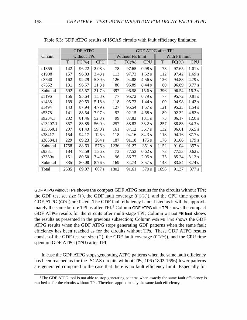
158 CHAPTER 6. TEST POINT INSERTION FOR DELAY FAULT ATPG
Table 6.3: GDF ATPG results of ISCAS circuits with fault efficiency limitation
GDF ATPG GDF ATPG after TPICircuit without TPs Without FE limit With FE limit
T FC(%) CPU T FC(%) CPU T FC(%) CPU
c1355 142 96.22 2.08 s 78 97.65 0.98 s 78 97.65 1.01 sc1908 157 96.83 2.43 s 113 97.72 1.62 s 112 97.42 1.69 sc3540 162 92.29 5.89 s 126 94.88 4.56 s 126 94.88 4.79 sc7552 131 96.67 11.3 s 80 96.89 8.44 s 80 96.89 8.77 sSubtotal 592 95.57 21.7 s 397 96.58 15.6 s 396 96.54 16.3 ss1196 156 95.64 1.33 s 77 95.72 0.79 s 77 95.72 0.81 ss1488 139 89.53 5.18 s 118 95.73 1.44 s 109 94.98 1.42 ss1494 143 87.94 4.79 s 127 95.54 1.57 s 121 95.23 1.54 ss5378 141 88.54 7.97 s 92 92.15 4.68 s 89 92.32 4.82 ss9234.1 232 81.46 52.3 s 99 87.82 13.1 s 73 86.17 12.0 ss13207.1 357 83.85 56.0 s 257 88.83 33.2 s 257 88.83 34.3 ss15850.1 207 81.43 59.0 s 161 87.12 36.7 s 132 86.61 35.5 ss38417 154 94.17 125 s 118 94.16 84.3 s 118 94.16 87.7 ss38584.1 229 89.23 264 s 187 91.18 175 s 176 91.06 179 sSubtotal 1758 88.63 576 s 1236 91.27 351 s 1152 91.04 357 ss938a 184 78.59 1.36 s 73 77.53 0.62 s 73 77.53 0.62 ss3330a 151 80.50 7.40 s 96 86.77 2.95 s 75 85.24 3.12 sSubtotal 335 80.08 8.76 s 169 84.74 3.57 s 148 83.54 3.74 s
Total 2685 89.07 607 s 1802 91.61 370 s 1696 91.37 377 s
GDF ATPG without TPs shows the compact GDF ATPG results for the circuits without TPs;the GDF test set size (T ), the GDF fault coverage (FC(%)), and the CPU time spent onGDF ATPG (CPU) are listed. The GDF fault efficiency is not listed as it will be approxi-mately the same before TPI as after TPI.1 Column GDF ATPG after TPI shows the compactGDF ATPG results for the circuits after multi-stage TPI; Column without FE limit showsthe results as presented in the previous subsection; Column with FE limit shows the GDFATPG results when the GDF ATPG stops generating GDF patterns when the same faultefficiency has been reached as for the circuits without TPs. These GDF ATPG resultsconsist of the GDF test set size (T ), the GDF fault coverage (FC(%)), and the CPU timespent on GDF ATPG (CPU) after TPI.
In case the GDF ATPG stops generating ATPG patterns when the same fault efficiencyhas been reached as for the ISCAS circuits without TPs, 106 (1802-1696) fewer patternsare generated compared to the case that there is no fault efficiency limit. Especially for
1The GDF ATPG tool is not able to stop generating patterns when exactly the same fault efficiency isreached as for the circuits without TPs. Therefore approximately the same fault efficiency.
6.2. EXPERIMENTAL RESULTS OF TPI FOR SAF ATPG ON GATE-DELAY FAULTATPG 159
circuits s9234.1 (-26 patterns), s15850.1 (-29 patterns), and s3330a (-21 patterns) fewerGDF patterns are generated with the fault efficiency limit.
Because fewer GDF patterns are generated due to the fault efficiency limit, the faultcoverages after GDF ATPG are not as high as the GDF fault coverages without the faultefficiency limit; i.e., 91.37% with fault efficiency limit versus 91.61% without fault ef-ficiency limit. Especially the fault coverages for circuits s1488, s9234.1, s15850.1 ands3330a with the fault efficiency limit are less than without the fault efficiency limit. Thisis not strange as for these circuits the number of GDF patterns has reduced the most withthe fault efficiency limit. Still the GDF fault coverage is significantly higher than for thecircuits without TPs, 91.37% versus 89.07%.
The CPU times do not differ much. The CPU times with the fault efficiency limitare even larger than the CPU times without fault efficiency limit, 377 seconds versus 370seconds. This can be partially explained by ATPG CPU time variations and by the factthat it takes time to check if a certain fault efficiency has been reached.
Also for the industrial benchmark circuits fewer GDF patterns are generated in casethe GDF ATPG stops generating patterns when the same fault efficiency has been reachedas for the circuits without TPs; for the Boolean circuits 1149 (10,452-9303) fewer patternsare generated, and for the three-state circuits 4219 (8366-4147) fewer patterns. Especiallyfor the three-state circuits the difference in number of GDF patterns is very large. Againthe results for circuit p66171 are the cause of this large difference. Without TPs it takesthe GDF ATPG tool 36 hours (129,635 seconds to be exactly) to generate GDF patternsfor only 41.09% of the detectable GDF faults. After TPI, it has become much easier forthe GDF ATPG tool to generate GDF patterns. In only 2005 seconds, the GDF ATPGreaches the 41% fault efficiency level after the generation of only 173 patterns. Withoutthe fault efficiency limit, the GDF ATPG continues generating patterns until the time limitof 36 hours has been reached. At that time 2777 patterns have been generated resultingin a GDF fault coverage of 85.55%, far more than the 39.01% fault coverage after GDFATPG with the fault efficiency limit.
Not only for circuit p66171, the number of GDF ATPG patterns has reduced signif-icantly in case the FE limit is used. Also for circuits p162057 (-643 patterns), p104649(-988 patterns), and p114605 (-290 patterns) the reduction is large. But as seen before,this reduction is at the cost of a lower fault coverage.
For the Boolean industrial circuits the fault coverage has been reduced from 92.54%without fault efficiency limit to 91.62% with this limit. For the three-state circuits, theGDF fault coverage has been reduced from 90.42% without fault efficiency limit to 84.98%with fault efficiency limit. This large difference for the three-state circuits is mostlycaused by circuit p66171, as explained above.
The GDF ATPG CPU times with and without fault efficiency limit for the Booleanindustrial circuits do not differ much; 17,448 seconds without limit compared to 17,113seconds with the limit. On the other hand, the GDF CPU times for the three-state indus-trial circuits differ enormously; 167,976 seconds without fault efficiency limit compared

160 CHAPTER 6. TEST POINT INSERTION FOR DELAY FAULT ATPG
Table 6.4: GDF ATPG results of industrial circuits with fault efficiency limitation
GDF ATPG GDF ATPG after TPICircuit without TPs Without FE limit With FE limit
T FC(%) CPU T FC(%) CPU T FC(%) CPU
p7653 660 90.98 107 s 465 93.24 52.9 s 435 92.73 52.8 sp13138 134 95.35 22.8 s 110 96.10 16.1 s 110 96.10 16.8 sp14148 623 90.50 155 s 384 89.66 116 s 382 89.63 120 sp27811 273 82.46 301 s 151 83.47 190 s 129 83.04 194 sp31025 1185 94.19 1343 s 1014 95.06 941 s 966 94.87 908 sp34592 310 98.48 320 s 268 99.13 239 s 229 98.69 248 sp36503 615 83.68 647 s 431 88.10 327 s 370 87.51 322 sp43282 747 92.60 1078 s 580 93.63 815 s 535 93.08 836 sp43663 296 94.24 191 s 238 94.69 157 s 235 94.68 165 sp72767 603 93.02 5036 s 439 93.80 2019 s 342 93.07 1996 sp73133 629 93.29 3368 s 431 94.01 2012 s 323 93.26 1921 sp73257 5697 87.21 7389 s 4612 87.37 5725 s 4607 87.36 6153 sp75344 477 91.92 1156 s 342 93.05 824 s 296 92.89 823 sp162057 3578 87.47 18431 s 987 93.13 4008 s 344 90.37 3351 sSubtotal 15827 90.50 39551 s 10452 92.54 17448 s 9303 91.62 17113 sp32118 1189 82.50 915 s 592 85.40 440 s 463 84.30 470 sp37021 358 38.87 185 s 240 44.27 132 s 191 43.61 133 sp66171 1067 37.44 129635 s 2777 85.55 129672 s 173 39.01 2005 sp71553 220 96.67 1497 s 169 96.75 1193 s 176 96.75 1147 sp93140 668 93.88 3450 s 499 94.08 2323 s 467 93.94 2419 sp104649 1956 89.60 11975 s 1636 94.25 6453 s 648 91.16 5519 sp114605 2332 95.03 16641 s 1743 95.76 7758 s 1453 95.21 8239 sp137498 1082 92.09 4802 s 710 93.22 2554 s 576 92.97 2473 sSubtotal 8872 83.98 169104 s 8366 90.42 150528 s 4147 84.98 22408 s
Total 24699 87.37 208655 s 18818 91.52 167976 s 13450 88.42 39521 s
to 39,521 seconds with the limit. Again this is mainly caused by circuit p66171. Withoutthe fault efficiency limit, the GDF ATPG consumes 36 hours, while with the fault effi-ciency limit, the GDF ATPG only consumes 2005 seconds.
Over all industrial circuits, the number of compact GDF ATPG patterns is reducedfrom 18818 patterns without the fault efficiency limit to 13450 patterns with the limit;in other words a reduction of 28.5%. However, this GDF pattern reduction is at the costof a GDF fault coverage reduction. The GDF fault coverage is reduced from 91.52%without the limit to 88.42% with the limit. Still the GDF fault coverage after TPI withthe fault efficiency limit is 1.05% higher than for the circuits without TPs; 88.42% versus
6.3. SUMMARY AND CONCLUSIONS 161
87.37%. The GDF ATPG CPU times in case of the fault efficiency limit are enormouslyreduced compared to the GDF ATPG CPU times without the fault efficiency limit. Butthis difference is mainly caused by circuit p66171.
6.3 Summary and conclusions
Besides facilitating compact SAF ATPG in generating compact test sets, TPI shouldalso be able to facilitate the generation of tests for other fault models. In this chapter wehave tested the impact of multi-stage TPI, as described in Chapter 5, on test sets generatedby a compact GDF ATPG.
The GDF ATPG, on which the impact of TPI has been tested, is a gross GDF ATPGthat uses the Transition Fault (TF) model. Experimental results of multi-stage TPI onGDF ATPG show that for both the ISCAS and the industrial benchmark circuits signif-icant test set size reductions can be achieved; 32.9% GDF test set size reduction for theISCAS circuits, and 34.0% for the Boolean industrial circuits. For the three-state indus-trial circuits 5.7% reduction has been achieved. This lower reduction is caused by theresults for circuit p66171. Within the time limit for the GDF ATPG of 36 hours, 1067patterns were generated for only 41% of the detectable faults. After TPI, the GDF ATPGwas able to generate 2777 patterns for 89% of the faults within 36 hours. A lot more pat-terns, but also a more than twice higher GDF fault coverage. Without taking into accountcircuit p66171, 28.4% GDF test set size reduction is achieved for the three-state industrialcircuits.
Besides a significant impact on the GDF test set sizes, multi-stage TPI also results insignificant GDF fault coverage improvements. The GDF fault coverage for the ISCAScircuits improve from 89.07% to 91.61%, for the Boolean industrial circuits from 90.50%to 92.54% and for the three-state industrial circuits from 83.98% to 90.42%. The largedifference in fault coverage for the three-state circuits is again caused by circuit p66171,as explained above. Without circuit p66171, the fault coverages for the three-state circuitsimprove from 89.20% without TPs to 90.97% after TPI.
Like for SAF ATPG, TPI also results in large GDF ATPG CPU time reduction. TheGDF ATPG CPU times reduction is 39% for the ISCAS circuits, 55.9% for the Booleanindustrial circuits, and 11.0% for the three-state industrial circuits. Without taking intoaccount circuit p66171, which causes the poor CPU time reduction for the three-state cir-cuits, the CPU reduction is 47.2%.
The GDF fault coverage improvement after TPI has a negative impact on the GDF testset size reduction. For the GDFs that have become detectable after TPI, also GDF patternshave to be generated by the ATPG. To get the impact of TPI on GDF test set sizes withoutthe negative impact of the fault coverage improvement, also GDF ATPG runs with a limiton the fault efficiency have been performed on the circuits after TPI. The GDF ATPG hasto stop generating patterns for the circuits after multi-stage TPI as soon as the same fault

162 CHAPTER 6. TEST POINT INSERTION FOR DELAY FAULT ATPG
efficiency has been reached as for the circuits without TPs.With the fault efficiency limit indeed better GDF test set size reductions have been
achieved. Compared to GDF ATPG without the fault efficiency limit, the GDF test setsizes reduce from 1802 patterns to 1696 patterns for the ISCAS circuits, from 10,452 pat-terns to 9303 patterns for the Boolean industrial circuits, and from 8366 to 4147 patternsfor the three-state industrial circuits. Especially the reduction for the three-state circuitsis very large. Again this is for a large part caused by circuit p66171.
Due to the fault efficiency limit, of course the GDF fault coverages are not as high aswithout the fault efficiency limit. Still higher fault coverages have been achieved than forthe circuits without TPs.
The difference in GDF CPU times between the GDF ATPG results with and withoutfault efficiency limit is not very high, except for the three-state industrial circuits. With thefault efficiency limit, the GDF ATPG stops generating GDF patterns for circuit p66171after 2005 seconds, while without this limit it generates patterns for 36 hours.
The compact GDF ATPG results after TPI for SAF ATPG, i.e., multi-stage TPI, pre-sented in this chapter, have shown that TPI is also capable of significantly reducing GDFATPG test set sizes. Not only the GDF test set sizes reduce, also the fault coverages thatcan be achieved with GDF ATPG increase significantly after TPI. The increase in GDFfault coverages has a negative impact on the GDF test set size reductions. As a result,the GDF test set size reductions are not as high as the SAF ATPG test set size reductions.On the other hand, the improvements in GDF fault coverages also result in a significantimprovement of the quality of the GDF tests. The GDF ATPG CPU times can be verylarge as shown for circuit p66171. TPI results in large GDF ATPG CPU time reductions.GDF CPU time reductions up to 78.3% for circuit p162057 have been achieved. For cir-cuit p66171, the GDF CPU time reduction was even 99%, given the same fault efficiencybefore and after TPI.
Overall, the experimental results given in this chapter have shown that TPI for SAFATPG can significantly facilitate GDF ATPG, resulting in smaller test sets, higher faultcoverages and lower ATPG times.

CHAPTER 7
Summary and conclusions
This final chapter provides a summary of the main subjects of this dissertation, anoverview of the main contributions, and topics for further research.
In Chapter 1 it has been motivated that the IC-manufacturers need high quality struc-tural tests for their integrated circuits. These high quality tests are necessary to make surethat as few as possible malfunctioning ICs are shipped to customers. These structuraltests can be performed on-chip and off-chip, i.e., with testers. Off-chip testing has theadvantage that high fault coverages can be achieved, but expensive testers are requiredwith a lot of memory. For on-chip testing, or Built-In Self-Test (BIST), no expensivetesters are required, but the fault coverages that can be achieved with on-chip testing arelower and on-chip testing means silicon overhead. Because the increasing complexity ofnowadays ICs makes the external testers more and more costly, BIST becomes more andmore interesting. But before BIST can successfully be used for a circuit, the BIST faultcoverages have to be high enough to meet the test quality demands of the customers ofthe IC-manufacturer.
Test Point Insertion (TPI) can be used to improve the testability of circuits. By theinsertion of Control Points (CPs) and Observation Points (OPs) it becomes easier to ac-tivate faults and to propagate fault effects to circuit outputs. This suggests that TPI canhelp to improve the fault coverage for on-chip testing, and to reduce the high costs oftesters for off-chip testing, by reducing the number of test patterns and the tester memoryrequirements. Not every position in the circuit is suitable for Test Points (TPs). Althoughseveral TPI algorithms exist, most of them assume Boolean circuits and cannot cope withindustrial circuits, with high impedance and unknown values, that are found in the realworld. Inserting TPs at wrong chosen positions can result in circuit damage.
One of the targets in this dissertation is to investigate on-chip methods with which thefault coverage can be improved without a large silicon overhead, and which can cope withindustrial (three-state) circuits. The other targets consist of investing existing TPI meth-ods and developing new TPI methods for improving on-chip fault coverage and off-chiptest set size reduction. These TPI methods should not only be applicable to small Boolean
163

164 CHAPTER 7. SUMMARY AND CONCLUSIONS
circuits, but also to large industrial designs. The targets described in this dissertation aresummarized chapter-wise:
Chapter 2: BIST The purpose of BIST is to embed a test on-chip in order to reduceexternal tester requirements. However, due to Random Pattern Resistant (RPR) faults inthe circuits, the fault coverages achievable with BIST are often not high enough to meetthe high quality requirements of the IC industry. Also a successful BIST implementationimplies several restrictions on a circuit, especially with respect to three-state circuits.
Several state-of-the-art BIST methods have been described with which higher faultcoverages can be achieved. These state-of-the-art BIST methods have been divided intomethods that modify the Pseudo-Random (PR) test patterns, methods that embed a fullset of deterministic test patterns, and methods that only embed parts of deterministic testpatterns.
The BIST methods that modify the generated test patterns or partially embed deter-ministic test patterns, are capable of increasing the fault coverages significantly, up tocomplete coverage. However, especially for RPR circuits, reaching a high or a completefault coverage is at the cost of a significant silicon overhead, often over 10% and some-times even over 100%. Also the BIST methods which embed full sets of deterministicpatterns have significant silicon overhead, sometimes over 100%.
When the silicon overhead of BIST methods is too high for successful BIST imple-mentation, one can consider redesigning the circuit, or the insertion of Test Points (TPs)to make the IC better testable. Although this impacts the design process, it helps improv-ing the BIST fault coverage and reducing the silicon overhead of BIST.
Chapter 3: Test Point Insertion TPI improves the testability of a circuit. CPs canbe inserted to improve the controllability of lines and OPs to improve the observability oflines. Besides the traditional AND/OR CP, the transparent scan flipflop (TSFF) is intro-duced as TP. A categorization of TPI methods is given; it depends on the method used todetermine the faults which testability should be improved; i.e., a method based on ATPG,fault simulation or testability analysis (TA). TPI methods can also be divided into test setdependent and test set independent methods. In case of industrial circuits, TPI algorithmsshould be able to cope with industrial circuits and avoid bus-conflicts. Also no TPs shouldbe allowed at the critical to avoid performance loss.
Several existing state-of-the-art TPI algorithms have been described for improvingBIST fault coverage, among the Cost Reduction Factor (CRF) TPI algorithm of Seiss[Sei91], the Hybrid CRF (HCRF) TPI algorithm of Tsai [Tsa97] and the Multi-phaseTPI (MTPI) algorithm of Tamarapalli [Tam96]. These three TPI algorithms assume aSTUMPS based architecture, and both the CRF and HCRF TPI algorithm use a cost func-tion, based on COP TA measures, to select the best TP positions. Therefore the STUMPSarchitecture, the COP TA measures, the cost function and cost gradients have been de-scribed first.
In Chapters 4 to 6 several TPI issues are addressed. An overview of these topics is

165
given including a description of benchmark circuits, i.e., ISCAS and Philips benchmarkcircuits, that have been used to test the new TPI techniques and algorithms proposed inChapters 4 to 6.
Chapter 4: Test Point Insertion for BIST In Chapters 4 to 6, the HCRF TPI al-gorithm has been used as a base for further TPI development. It is described why thisalgorithm has been chosen. The HCRF TPI algorithm assumes Boolean circuits and doesnot take into account any implications with respect to industrial circuits. A new TPI algo-rithm has been proposed, based on the HCRF TPI algorithm, that can cope with industrialcircuits and results in even better BIST fault coverage improvement after TPI. Also a newcost function, the NPAT cost function, has been proposed for this new TPI algorithm toimprove the BIST fault coverage after TPI even further. In order to cope with industrialcircuits, the COP TA measures, cost function and gradients calculations have been ex-tended such that they can be used in combination with high impedance values, unknownvalues, and three-state elements.
Experimental results of the proposed NPAT TPI algorithm for industrial circuits haveshown that better BIST fault coverages can be achieved than with the original Hybrid CRFTPI algorithm of Tsai, on both Boolean and industrial (three-state) circuits. The resultsalso show that the algorithm can be applied to small circuits and large complex industrialdesigns.
A method has been introduced that reduces the number of TP candidates in the circuit,such that the CPU time spent by the NPAT TPI algorithm is reduced without impactingthe quality of the TP selection.
Chapter 5: Test point insertion for compact SAF ATPG The growth in ATPG testset sizes, caused by the increasing complexity of circuits, has a major impact on the ATEdemands for the semiconductor industry. Experimental results have shown that NPATTPI, that is only targeted at improving the BIST fault coverage for a circuit, is already ca-pable of significantly reducing compact ATPG test set sizes. Also the stuck-at fault (SAF)ATPG fault coverages improve, and the ATPG CPU times reduce after NPAT TPI. Stillseveral ATPG specific testability issues were not yet solved, resulting in a not optimal testset size reduction for several circuits, i.e., less than 10%. A new cost function has beenproposed that takes into account test counts (TCs). TCs give a lower bound on the ATPGtest set size, given complete fault coverage. High TC measures in a circuit indicate thatthe ATPG test set size will also be high. With the proposed TC-based cost function, theTPI algorithm will also try to reduce the TCs in the circuit in order to reduce the ATPGtest set size. Experimental results show that with the TPI algorithm that takes into ac-count TCs, i.e., TC&COP TPI, in general better test set size reduction can be achieved,i.e., 1.7% better reduction for the ISCAS benchmark circuits up to 17% better reductionfor the industrial benchmark circuits.
Also after TC&COP TPI there are still circuits with disappointing test set size reduc-tions. These circuits often suffer from very large fan-out free regions (FFRs). Although

166 CHAPTER 7. SUMMARY AND CONCLUSIONS
the FFR outputs have high TC values, the TC&COP TPI and NPAT TPI algorithm donot always insert TPs in these large FFRs to reduce the TC values. Therefore, the TPIalgorithm has been extended with a TPI pre-process that inserts TPs to reduce the FFRsizes within the circuit. Four TPI methods for reducing large FFRs have been describedto identify and reduce the large FFRs. With this TPI pre-process, also for the circuits thatsuffer from very large FFRs, the test set sizes can be reduced significantly.
Because each circuit suffers from different testability problems (related to SAF ATPG),the multi-stage TPI algorithm has been developed. The TPI process is divided into mul-tiple stages. In each stage a TPI pre-process is applied, that analyzes the TA measuresto select a cost function aimed at solving the testability problems of that specific circuit.With this cost function several TPs are inserted, after which the TPI pre-process is runagain to select a new cost function. After multi-stage TPI, that also includes TPI for re-ducing large FFRs, extra reductions of 4.5% for the ISCAS circuits and 12.2% for theindustrial circuits have been achieved compared to TC&COP TPI.
Chapter 6: Test Point Insertion for delay fault ATPG Besides facilitating SAFATPG in generating compact test sets, TPI should also be able to facilitate the generationof tests for other fault models. The impact of TPI for SAF ATPG, i.e., multi-stage TPI, hasbeen tested on gate-delay fault (GDF) ATPG, i.e., Transition Fault ATPG. Experimentalresults have shown that indeed significant GDF test set size reductions can be achievedwith TPI for SAF ATPG; on average 32.9% for the ISCAS circuits and 23.8% for the in-dustrial circuits. For several circuits also the GDF fault coverage increased considerably.This increase in GDF ATPG fault coverage has a negative impact on the GDF test set sizereduction; the GDF ATPG also has to generate patterns for the GDFs that have becomedetectable after TPI. Due to the much larger GDF fault coverage increase than SAF faultcoverage increase, the GDF test set size reduction was not as high as the SAF test set sizereduction.
Altering the experimental setup such that the GDF ATPG stops generating patternsfor the circuits with TPs as soon as the same fault efficiency has been reached as for thecircuits without TPs, results in a reduction of the negative impact of the GDF fault cov-erage improvement. The experimental results have shown that indeed better GDF test setsize reductions have been achieved. The GDF test set size reduction increased to 36.8%for the ISCAS circuits and to 45.5% for the industrial circuits.
Besides reducing the GDF test set sizes and improving the GDF fault coverage, TPIalso resulted in significant GDF ATPG CPU time reductions, up to 99%.

7.1. MAJOR CONTRIBUTIONS 167
7.1 Major contributions
The major contributions of this research are:
On-chip testing (BIST) [Chapter 2]
1. Investigation and categorization of existing state-of-the art on-chip test methods,i.e., BIST methods.
2. An analysis and comparison of the existing BIST methods with respect to hardwareoverhead and pseudo-random fault coverage. In general will random pattern resis-tant circuits result in (too) large silicon overhead for BIST methods to be applicable.
3. An analysis of the existing BIST methods whether they are only applicable to smallbenchmark circuits, or also to large industrial designs.
Test Point Insertion for BIST
1. A categorization of TPI methods [Section 3.3].
2. Investigation of existing state-of-the-art TPI algorithms [Section 3.7].
3. An analysis and comparison of three TPI algorithms that improve pseudo randomfault coverage with respect to [Section 4.1]:
• the number of inserted test points versus the pseudo random fault coverage,
• the application on Boolean and industrial circuits,
• the application on large circuits.
4. The extension of the Hybrid CRF TPI algorithm such that it can be used for im-proving the pseudo random fault coverage of both Boolean as well as industrial(three-state circuits). This has been accomplished by adding three-state and un-known value capabilities to [Sections 4.2,4.3][Geu03]:
• COP,
• cost function,
• cost gradients.
5. The development of a new cost function for the extended Hybrid CRF TPI methodfor industrial circuits in order to further improve the pseudo-random fault coverageafter TPI [Section 4.3][Geu03].
6. The development of a method to reduce the number of test point candidates thatresults in a TPI CPU time reduction without impacting the quality of the test pointselection [Section 4.3][Geu02a].
168 CHAPTER 7. SUMMARY AND CONCLUSIONS
Test Point Insertion for stuck-at fault ATPG
1. An evaluation of the impact of TPI for BIST on reducing stuck-at fault ATPG testset sizes [Section 5.1][Geu00].
2. An analysis of which testability problems cause large ATPG test sets, i.e., largeFFRs and high test counts [Sections 5.2,5.4][Geu00, Geu02b].
3. The development of a new TPI algorithm that takes into account test counts suchthat the TPI algorithm becomes more aimed at reducing ATPG test set sizes. Thisis accomplished by [Section 5.3][Geu00, Geu01]:
• defining a heuristic for propagating test counts in a circuit with fan-outs,
• the development of a cost function that takes into account both COP and testcounts testabilities,
• defining the test counts gradient equations,
• extending the HCRF TPI algorithm for industrial circuits with an extra event-driven forward and backward propagation step of changed test counts due toa TP.
4. The development of a TPI pre-process to reduce large FFRs in a circuit as largeFFRs often cause large stuck-at fault ATPG test sets [Section 5.4][Geu02b].
5. The development of a multi-stage TPI algorithm. In each stage of the TPI process,a cost function is selected, based on testability analysis measures, that targets thehighest testability problems found in the circuit, given already inserted test pointsin previous stages [Section 5.5][Geu02b].
TPI for gate-delay fault ATPG
1. The application of TPI has been tested on another fault model, the gross gate-delayfault. An analysis is given of the impact of multi-stage TPI, on gate-delay faultATPG, i.e., transition fault ATPG. The following gate-delay fault ATPG resultshave been analyzed before and after multi-stage TPI [Section 6.2][Geu02b]:
• The gate-delay fault test set size reduction, together with the gate-delay faultcoverage improvement, and the gate-delay fault ATPG CPU time reduction.
• The gate-delay fault test set size reduction only, as the gate-delay fault cov-erage improvement has a negative impact on the gate-delay fault test set sizereduction.
Experimental results have demonstrated that the proposed TPI for BIST algorithm,i.e., NPAT TPI, is applicable to small and large designs, both Boolean and industrial,
7.2. SUGGESTED TOPICS FOR FUTURE RESEARCH 169
and that in general better fault coverage improvements can be achieved that with existingstate-of-the-art TPI algorithms [Geu03]. The pseudo random fault coverage for industrialcircuits has been improved from 93.53% with the original Hybrid CRF TPI algorithm forindustrial circuits to 94.49% with NPAT TPI, see Table 4.5. In other words 15% of thefaults that were not covered after TPI with the original cost function, have become cov-ered after NPAT TPI.
NPAT TPI also facilitates stuck-at fault ATPG in reducing ATPG test sets, improv-ing the ATPG fault coverage and reducing the ATPG CPU times [Geu00]. On aver-age, the ATPG test set sizes of the Boolean and industrial benchmark circuits have beenreduced with 43%, respectively 26%. The presented TPI for SAF ATPG algorithms,i.e., TC&COP TPI and multi-stage TPI (including the TPI for reducing large FFRs pre-process) significantly improve the facilitation of SAF ATPG compared to NPAT TPI[Geu00, Geu01, Geu02b]. On average, the stuck-at fault ATPG test set sizes have beenreduced with 47% for the Boolean, respectively 51% for the industrial circuits comparedto the circuits without test points.
It has been shown that multi-stage TPI does not only facilitates stuck-at fault ATPG,but also gate-delay fault ATPG [Geu02b]. The average gate-delay fault ATPG test set sizereduction after TPI was 37% for the Boolean, respectively 46% for the industrial circuits,given the same gate-delay fault efficiency before and after TPI. Also the impact of TPIon the gate-delay fault coverage and ATPG times is significant. For circuit p66171, thegate-delay fault ATPG time for generating patterns for 41% of all detectable faults, isreduced from 36 hours without TPI to 2005 seconds after TPI. After TPI, the gate-delayfault ATPG was able to generate in 36 hours patterns for 89% of all detectable faults,compared to the 39% for the circuit without test points.
The proposed new TPI algorithms and techniques, i.e., NPAT TPI, TC&COP TPI,TPI for reducing large FFRs, multi-stage TPI, and the TPI candidates reduction tech-nique, have been implemented and integrated in the Delft Advanced Test (DAT) gener-ation system and AMSAL, and are being used worldwide within Philips as part of theirlogic test tool set. The robustness and application of the TPI algorithms on very largeindustrial designs have been proven at Philips as the TPI algorithms are currently appliedto multi-million gate designs.
7.2 Suggested topics for future research
A state-of-the art TPI tool has been developed. It improves PR fault coverage foron-chip testing, and significantly reduces compact SAF and GDF ATPG test set sizes forboth Boolean and three-state circuits. However, for both on- and off-chip testing, thereare still several TPI related topics for which we suggest further research.
With respect to TPI for BIST, i.e., on-chip-testing, we suggest the following topics:

170 CHAPTER 7. SUMMARY AND CONCLUSIONS
1. The integration of the Hybrid TPI algorithm for industrial circuits with a state-of-the-art BIST method and comparing the BIST fault and silicon overhead with otherstate-of-the-art TPI+BIST solutions, i.e., MTPI BIST.
2. The development of TPI extensions for industrial circuits in order to:
• insert TPs for bypassing fixed circuit inputs, i.e., inputs from embedded mem-ories.
• add CPs between buses and circuit outputs, such that it can be prevented thatunknown values, caused by bus-conflicts, can corrupt the MISR state.
With respect to TPI for ATPG, we suggest the following topics:
1. Research and integration of other TA measures that indicate on large ATPG test setsizes, such that the ATPG test set sizes can be further reduced. The integration ofATPG data taken from an ATPG run for the circuit without TPs to find the ATPG’problem’ locations in the circuit, hence the best TP positions in the circuit.
2. An evaluation of the impact of TPI on other fault models than SAF and GDF ATPG,e.g., path-delay faults or bridge-faults.
3. Research of a GDF related TA measure and a TPI cost function that is specificallyaimed at reducing GDF ATPG test set sizes.
With respect to TPI in general, i.e., both for on-chip and off-chip testing, we suggest thefollowing topics:
1. Further reducing the number of TPI candidates without impacting the test quality,i.e., test set size reduction and/or fault coverage improvement.
2. Research how TPI can be optimally used for partial-scan circuits, i.e., circuits thatcontain SFFs but also non-scannable memory elements. In other words, TPI forcontrolling and observing non-scannable FFs, without impacting the critical path,hence the performance of the IC.
3. Research how TPI can help making untestable/redundant faults testable in testmode, without impacting the purpose of the redundancy, when such a purpose ex-ists.
4. An investigation of the impact on the test set size reduction and/or fault coverageimprovement when TPs on critical paths are avoided.
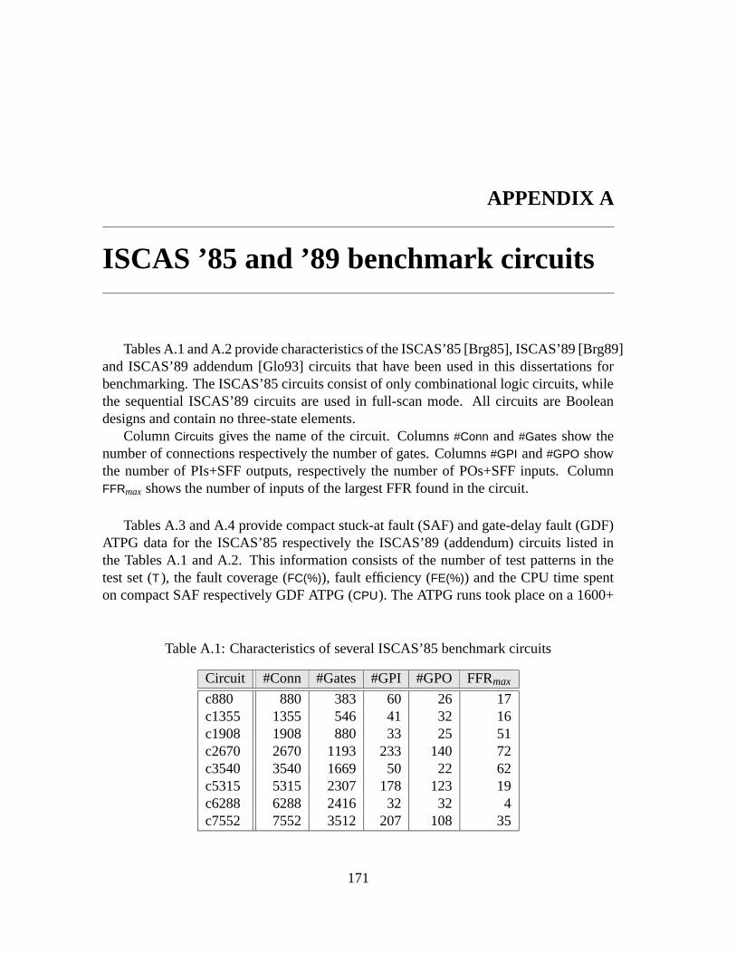
APPENDIX A
ISCAS ’85 and ’89 benchmark circuits
Tables A.1 and A.2 provide characteristics of the ISCAS’85 [Brg85], ISCAS’89 [Brg89]and ISCAS’89 addendum [Glo93] circuits that have been used in this dissertations forbenchmarking. The ISCAS’85 circuits consist of only combinational logic circuits, whilethe sequential ISCAS’89 circuits are used in full-scan mode. All circuits are Booleandesigns and contain no three-state elements.
Column Circuits gives the name of the circuit. Columns #Conn and #Gates show thenumber of connections respectively the number of gates. Columns #GPI and #GPO showthe number of PIs+SFF outputs, respectively the number of POs+SFF inputs. ColumnFFRmax shows the number of inputs of the largest FFR found in the circuit.
Tables A.3 and A.4 provide compact stuck-at fault (SAF) and gate-delay fault (GDF)ATPG data for the ISCAS’85 respectively the ISCAS’89 (addendum) circuits listed inthe Tables A.1 and A.2. This information consists of the number of test patterns in thetest set (T ), the fault coverage (FC(%)), fault efficiency (FE(%)) and the CPU time spenton compact SAF respectively GDF ATPG (CPU). The ATPG runs took place on a 1600+
Table A.1: Characteristics of several ISCAS’85 benchmark circuits
Circuit #Conn #Gates #GPI #GPO FFRmax
c880 880 383 60 26 17c1355 1355 546 41 32 16c1908 1908 880 33 25 51c2670 2670 1193 233 140 72c3540 3540 1669 50 22 62c5315 5315 2307 178 123 19c6288 6288 2416 32 32 4c7552 7552 3512 207 108 35
171
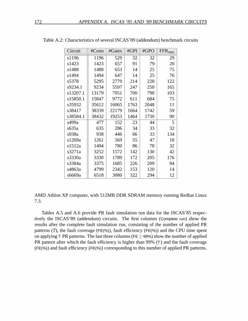
172 APPENDIX A. ISCAS ’85 AND ’89 BENCHMARK CIRCUITS
Table A.2: Characteristics of several ISCAS’89 (addendum) benchmark circuits
Circuit #Conn #Gates #GPI #GPO FFRmax
s1196 1196 529 32 32 29s1423 1423 657 91 79 20s1488 1488 653 14 25 75s1494 1494 647 14 25 76s5378 5295 2779 214 228 122s9234.1 9234 5597 247 250 165s13207.1 13179 7951 700 790 103s15850.1 15847 9772 611 684 75s35932 35612 16065 1763 2048 11s38417 38339 22179 1664 1742 59s38584.1 38432 19253 1464 1730 90s499a 477 152 23 44 5s635a 635 286 34 33 32s938a 938 446 66 33 134s1269a 1261 569 55 47 18s1512a 1494 780 86 78 32s3271a 3252 1572 142 130 42s3330a 3330 1789 172 205 176s3384a 3375 1685 226 209 94s4863a 4799 2342 153 120 14s6669a 6518 3080 322 294 12
AMD Athlon XP computer, with 512MB DDR SDRAM memory running Redhat Linux7.3.
Tables A.5 and A.6 provide PR fault simulation run data for the ISCAS’85 respec-tively the ISCAS’89 (addendum) circuits. The first columns (Complete run) show theresults after the complete fault simulation run, consisting of the number of applied PRpatterns (T), the fault coverage (FE(%)), fault efficiency (FE(%)) and the CPU time spenton applying T PR patterns. The last three columns (FE ≥ 99%) show the number of appliedPR pattern after which the fault efficiency is higher than 99% (T ) and the fault coverage(FE(%)) and fault efficiency (FE(%)) corresponding to this number of applied PR patterns.

173
Table A.3: ATPG characteristics of the ISCAS’85 circuits
Stuck-at fault ATPG Gate-delay fault ATPGCircuit T FC(%) FE(%) CPU T FC(%) FE(%) CPU
c880 28 100.00 100.00 0.27 s 34 97.35 97.35 0.37 sc1355 89 99.70 100.00 0.49 s 142 96.22 96.53 2.08 sc1908 114 99.71 100.00 1.32 s 157 96.83 97.07 2.43 sc2670 59 96.40 100.00 1.30 s 61 91.85 94.89 2.12 sc3540 119 96.38 100.00 2.59 s 162 92.29 95.74 5.89 sc5315 78 99.42 100.00 2.47 s 85 97.29 97.99 4.49 sc6288 32 99.46 100.00 2.77 s 77 99.22 99.90 14.1 sc7552 128 98.55 100.00 6.01 s 131 96.67 97.83 11.3 s
Table A.4: ATPG characteristics of the ISCAS’89 (addendum) circuits
Stuck-at fault ATPG Gate-delay fault ATPGCircuit T FC(%) FE(%) CPU T FC(%) FE(%) CPU
s1196 133 100.00 100.00 0.52 s 156 95.64 95.73 1.33 ss1423 39 99.09 100.00 0.35 s 72 86.31 97.17 1.15 ss1488 115 100.00 100.00 0.53 s 139 89.53 97.08 5.18 ss1494 117 99.46 100.00 0.52 s 143 87.94 96.01 4.79 ss5378 117 98.87 100.00 2.81 s 141 88.54 96.97 7.97 ss9234.1 135 93.95 99.91 20.0 s 232 81.46 92.86 52.3 ss13207.1 272 98.87 100.00 15.5 s 357 83.85 96.39 56.0 ss15850.1 128 97.51 100.00 13.9 s 207 81.43 96.30 59.0 ss35932 14 89.69 100.00 20.8 s 24 83.03 97.05 139 ss38417 88 99.68 100.00 30.9 s 154 94.17 96.12 125 ss38584.1 123 95.57 100.00 44.9 s 229 89.23 96.90 264 ss499a 104 100.00 100.00 0.28 s 66 68.43 99.78 0.34 ss635a 47 100.00 100.00 0.23 s 99 73.47 100.00 0.53 ss938a 145 100.00 100.00 0.45 s 184 78.59 96.09 1.36 ss1269a 38 100.00 100.00 0.33 s 54 94.38 95.22 0.71 ss1512a 64 100.00 100.00 0.41 s 74 84.12 90.51 2.67 ss3271a 59 100.00 100.00 1.03 s 77 94.70 97.51 3.08 ss3330a 163 100.00 100.00 2.20 s 151 80.50 90.90 7.40 ss3384a 74 100.00 100.00 1.04 s 96 98.89 98.91 2.89 ss4863a 48 100.00 100.00 1.94 s 87 96.77 97.78 9.10 ss6669a 35 100.00 100.00 2.29 s 59 99.68 99.68 5.76 s

174 APPENDIX A. ISCAS ’85 AND ’89 BENCHMARK CIRCUITS
Table A.5: PR Fault simulation results of the ISCAS’85 circuits
Complete run FE ≥ 99%Circuit T FC(%) FE(%) CPU T FC(%) FE(%)
c880 9024 100.00 100.00 0.18 s 2720 99.58 99.58c1355 2848 99.49 100.00 0.16 s 1312 98.60 99.11c1908 11520 99.52 100.00 0.47 s 2080 98.67 99.15c2670 32000 84.82 89.08 2.05 s - - -c3540 32000 95.97 99.97 2.30 s 1408 95.01 99.01c5315 3712 98.90 100.00 0.63 s 416 98.00 99.10c6288 128 99.56 100.00 0.49 s 64 99.33 99.77c7552 32000 95.30 97.03 6.17 s - - -
Table A.6: PR Fault simulation results of the ISCAS’89 (addendum) circuits
Complete run FE ≥ 99%Circuit T FC(%) FE(%) CPU T FC(%) FE(%)
s1196 32000 99.60 99.60 0.43 s 12864 99.03 99.03s1423 17568 99.08 100.00 0.35 s 2176 98.22 99.14s1488 3520 100.00 100.00 0.18 s 1536 99.13 99.13s1494 3520 99.20 100.00 0.17 s 1312 98.21 99.00s5378 32000 98.94 99.80 3.88 s 6816 98.13 99.00s9234.1 32000 87.05 93.49 10.0 s - - -s13207.1 32000 97.05 98.58 13.0 s - - -s15850.1 32000 92.83 96.14 15.4 s - - -s35932 224 89.81 100.00 1.05 s 96 89.06 99.26s38417 32000 94.42 94.95 46.5 s - - -s38584.1 32000 95.31 99.46 43.2 s 14080 94.85 99.00s499a 32000 41.85 41.85 0.36 s - - -s635a 32000 73.57 73.57 0.29 s - - -s938a 32000 64.98 64.98 0.48 s - - -s1269a 1056 100.00 100.00 0.14 s 256 99.33 99.33s1512a 32000 95.28 95.28 0.64 s - - -s3271a 32000 99.82 99.82 2.08 s 5984 99.24 99.24s3330a 32000 86.97 86.97 2.93 s - - -s3384a 32000 96.18 96.18 2.23 s - - -s4863a 32000 97.57 97.57 3.29 s - - -s6669a 4416 100.00 100.00 0.85 s 96 99.22 99.22

APPENDIX B
Industrial benchmark circuits
Tables B.1 and B.2 provide characteristics of the Philips industrial cores used in thisdissertation for benchmarking. Most of these industrial circuits are used in products, ex-cept for circuit p93140, which only has been designed for test purposes. The circuitslisted in Table B.1 are Boolean circuits, while the circuits listed in Table B.2 contain oneor more three-state elements.
Column Circuits gives the name of the circuit. Columns #Conn and #Gates show thenumber of connections respectively the number of gates. Columns #GPI and #GPO show
Table B.1: Characteristics of several Boolean Philips industrial benchmark circuits
Circuit #Conn #Gates #GPI #GPO FFRmax
p5973 6621 2979 245 225 35p7653 7653 3685 197 264 67p13138 13138 5901 498 440 52p14148 14148 6827 559 572 170p27811 27811 13247 1273 1403 96p31025 31025 14913 629 662 137p34592 34592 17685 408 651 92p36503 36503 19292 1502 1514 96p43282 43282 21484 1003 906 110p43663 43663 17865 8232 8249 56p72767 72767 35266 1923 1630 169p73133 73133 35675 1922 1629 169p73257 73257 37587 2353 2229 269p75344 75344 36561 3716 3742 181p162057 162057 77994 5914 5841 1518
175

176 APPENDIX B. INDUSTRIAL BENCHMARK CIRCUITS
Table B.2: Characteristics of several tri-state Philips industrial benchmark circuits
Circuit #Conn #Gates #GPI #GPO FFRmax
p32118 32118 14449 1572 1560 244p37021 37021 17059 2001 1843 96p66171 66192 27011 1002 1047 78p71553 71553 32691 762 520 19p93140 93140 47809 3331 2891 474p104649 104649 44619 3533 3466 244p114605 114605 57356 2754 2670 131p137498 137498 59240 6984 6592 433p481470 481470 237328 18564 18577 1044p596922 596922 313711 17768 17356 467p598004 598004 285355 20648 20084 1518p705050 705704 359615 30856 29916 256p824184 824184 453002 26124 24548 520p854266 855659 433361 32194 32303 292
the number of PIs+SFF outputs, respectively the number of POs+SFF inputs. ColumnFFRmax shows the number of inputs of the largest FFR found in the circuit.
Tables B.3 and B.4 provide compact SAF and GDF ATPG data for the Boolean re-spectively three-state industrial circuits listed in the previous tables. This informationconsists of the number of test patterns (T ), the fault coverage (FC), fault efficiency (FE)and the CPU time spent on compact SAF, respectively GDF ATPG, (CPU). Each run had aCPU time limit of 36 hours. Results with runs which took more than 36 hours are incom-plete, as ATPG did not finish yet. Because of the long GDF ATPG times and the limitedmemory capacity (512Mb) of the test computer, GDF ATPG has only been performed oncircuits with less than 200,000 signal lines. The ATPG runs took place on a 1600+ AMDAthlon XP computer, with 512MB DDR SDRAM memory running Redhat Linux 7.3.
Tables B.5 and B.6 provide PR fault simulation run data for the Boolean respectivelythree-state industrial circuits listed in the previous tables. Note that the PR results are onlyshown for the three-state circuits, which do not contain buses that can become in conflictdue to the application of PR patterns!
The first columns (Complete run) show the results after the complete fault simulationrun, consisting of the number of applied PR patterns (T ), the fault coverage (FC(%)), faultefficiency (FE(%)) and the CPU time spent after T PR patterns. The last three columns (FE
≥ 99%) show the number of applied PR pattern after which the fault efficiency is higherthan 99% (T ) and the fault coverage (FC(%)) and fault efficiency (FE(%)) corresponding tothis number of applied PR patterns.
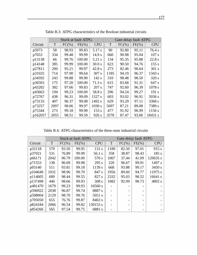
177
Table B.3: ATPG characteristics of the Boolean industrial circuits
Stuck-at fault ATPG Gate-delay fault ATPGCircuit T FC(%) FE(%) CPU T FC(%) FE(%) CPU
p5973 58 98.93 99.83 5.17 s 90 92.80 95.11 76.4 sp7653 334 99.48 99.99 14.9 s 660 90.98 95.04 107 sp13138 66 99.76 100.00 5.21 s 134 95.35 95.88 22.8 sp14148 385 99.99 100.00 30.0 s 623 90.50 94.76 155 sp27811 200 95.21 99.97 42.8 s 273 82.46 96.64 301 sp31025 714 97.90 99.64 307 s 1185 94.19 96.37 1343 sp34592 243 99.88 99.90 142 s 310 98.48 98.50 320 sp36503 175 97.20 100.00 71.3 s 615 83.68 91.31 647 sp43282 382 97.66 99.83 207 s 747 92.60 96.39 1078 sp43663 194 99.23 100.00 58.8 s 296 94.24 99.27 191 sp72767 438 96.31 99.09 1527 s 603 93.02 96.91 5036 sp73133 407 96.37 99.08 1492 s 629 93.29 97.11 3368 sp73257 2097 98.06 99.97 1030 s 5697 87.21 89.08 7389 sp75344 273 99.18 99.90 153 s 477 91.92 96.99 1156 sp162057 2055 98.51 99.59 926 s 3578 87.47 93.06 18431 s
Table B.4: ATPG characteristics of the three-state industrial circuits
Stuck-at fault ATPG Gate-delay fault ATPGCircuit T FC(%) FE(%) CPU T FC(%) FE(%) CPU
p32118 570 93.50 99.95 131 s 1189 82.50 97.01 915 sp37021 531 76.89 99.99 56.1 s 358 38.87 98.43 185 sp66171 2042 96.79 100.00 576 s 1067 37.44 41.09 129635 sp71553 138 96.69 99.98 295 s 220 96.67 99.91 1497 sp93140 511 93.81 99.18 1139 s 668 93.88 99.17 3450 sp104649 1031 98.96 99.70 847 s 1956 89.60 94.77 11975 sp114605 689 98.44 99.55 827 s 2332 95.03 98.52 16641 sp137498 446 98.66 99.93 308 s 1082 92.09 98.73 4802 sp481470 1679 99.23 99.93 16560 s - - - -p596922 2038 96.87 99.74 8887 s - - - -p598004 2129 98.70 99.76 5051 s - - - -p705050 655 76.76 99.87 8463 s - - - -p824184 2066 96.54 99.82 130153 s - - - -p854266 565 97.54 99.75 6881 s - - - -
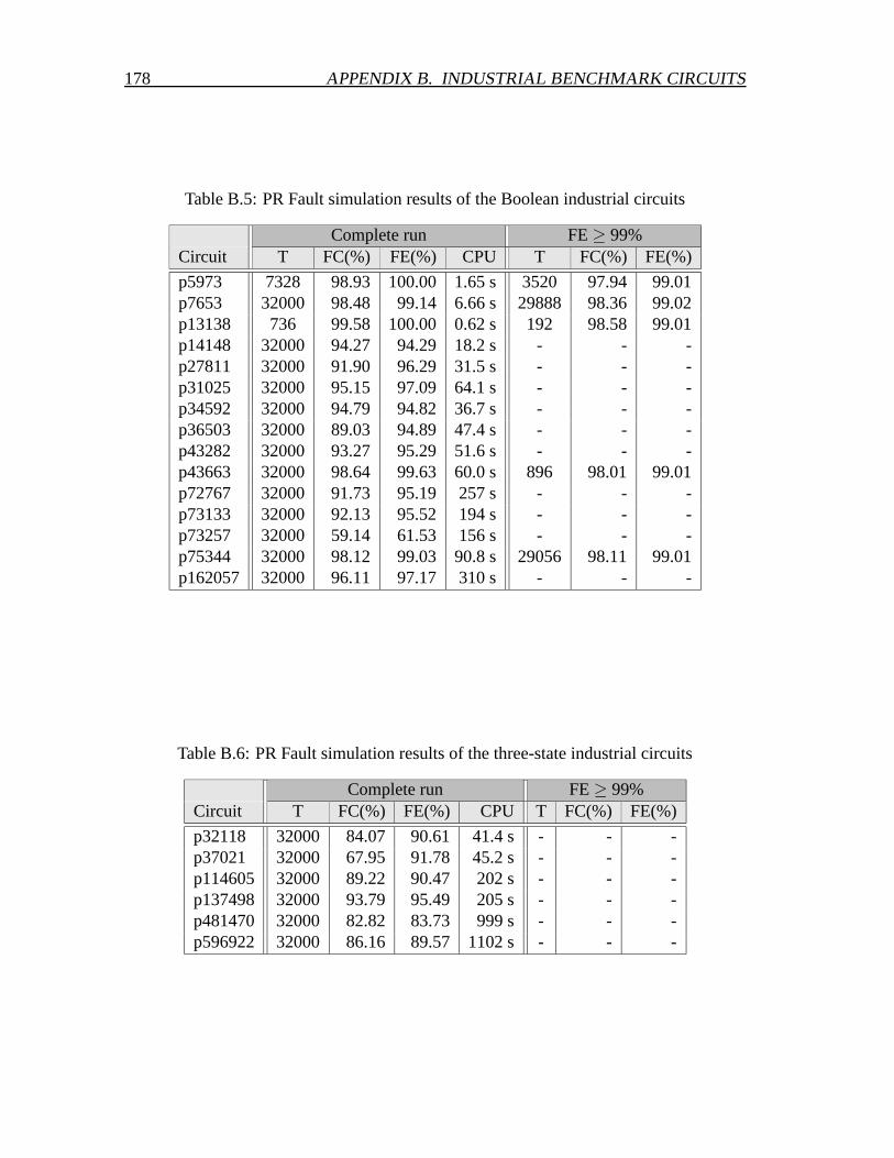
178 APPENDIX B. INDUSTRIAL BENCHMARK CIRCUITS
Table B.5: PR Fault simulation results of the Boolean industrial circuits
Complete run FE ≥ 99%Circuit T FC(%) FE(%) CPU T FC(%) FE(%)
p5973 7328 98.93 100.00 1.65 s 3520 97.94 99.01p7653 32000 98.48 99.14 6.66 s 29888 98.36 99.02p13138 736 99.58 100.00 0.62 s 192 98.58 99.01p14148 32000 94.27 94.29 18.2 s - - -p27811 32000 91.90 96.29 31.5 s - - -p31025 32000 95.15 97.09 64.1 s - - -p34592 32000 94.79 94.82 36.7 s - - -p36503 32000 89.03 94.89 47.4 s - - -p43282 32000 93.27 95.29 51.6 s - - -p43663 32000 98.64 99.63 60.0 s 896 98.01 99.01p72767 32000 91.73 95.19 257 s - - -p73133 32000 92.13 95.52 194 s - - -p73257 32000 59.14 61.53 156 s - - -p75344 32000 98.12 99.03 90.8 s 29056 98.11 99.01p162057 32000 96.11 97.17 310 s - - -
Table B.6: PR Fault simulation results of the three-state industrial circuits
Complete run FE ≥ 99%Circuit T FC(%) FE(%) CPU T FC(%) FE(%)
p32118 32000 84.07 90.61 41.4 s - - -p37021 32000 67.95 91.78 45.2 s - - -p114605 32000 89.22 90.47 202 s - - -p137498 32000 93.79 95.49 205 s - - -p481470 32000 82.82 83.73 999 s - - -p596922 32000 86.16 89.57 1102 s - - -

APPENDIX C
Boolean elements
The gate symbol, truth table and the COP TA measures are given for several Booleanprimitive elements. The symbols and truth tables are taken from [vdL96]. The truth tablesdo take into account the ’high impedance’ value Z and the ’unknown’ value U such thatthey are compatible with three-state circuits. In case of (N)AND and (N)OR gate, thetruth tables are shown for a two-input gate.
For all Boolean elements, the COP TA measures, extended for three-state logic, con-sist of the equations for C0, C1 and W . All CZs, WZ0, and WZ1 are 0, because Z valuescannot propagate through Boolean elements; they result in U values on the outputs. CUcan be found with CU = 1−C1−C0.
Buffer:z1x z x
0 1 Z U0 1 U U
C0z C0x
C1z C1x
Wx Wz
Inverter:z1x z x
0 1 Z U1 0 U U
C0z C1x
C1z C0x
Wx Wz
AND:
&x1
xz
X
z x1
0 1 Z U0 0 0 0 0
x2 1 0 1 U UZ 0 U U UU 0 U U U
C0z 1−∏Xi=1(1−C0xi)
C1z ∏Xi=1(C1xi)
Wx j Wz ·∏Xi=1,i6= j(C1xi)
179

180 APPENDIX C. BOOLEAN ELEMENTS
NAND:
&x1
xz
X
z x1
0 1 Z U0 1 1 1 1
x2 0 1 0 U UZ 1 U U UU 1 U U U
C0z ∏Xi=1(C1xi)
C1z 1−∏Xi=1(1−C0xi)
Wx j Wz ·∏Xi=1,i6= j(C1xi)
OR:
x
x 1 zX
1z x1
0 1 Z U0 0 1 U U
x2 1 1 1 1 1Z U 1 U UU U 1 U U
C0z ∏Xi=1 C0xi
C1z 1−∏Xi=1(1−C1xi)
Wx j Wz ·∏Xi=1,i6= j(C0xi)
NOR:
x1
x 1 zX
z x1
0 1 Z U0 1 0 U U
x2 1 0 0 0 0Z U 0 U UU U 0 U U
C0z 1−∏Xi=1(1−C1xi)
C1z ∏Xi=1 C0xi
Wx j Wz ·∏Xi=1,i6= j(C0xi)
XOR:
x1
x2
z=1
z x1
0 1 Z U0 0 1 U U
x2 1 1 0 U UZ U U U UU U U U U
C0z C0x1 ·C0x2 +C1x1 ·C1x2
C1z C0x1 ·C1x2 +C1x1 ·C0x2
Wx1 Wz · (C0x2 +C1x2)
NXOR:
x1
x2=1 z
z x1
0 1 Z U0 1 0 U U
x2 1 0 1 U UZ U U U UU U U U U
C0z C0x1 ·C1x2 +C1x1 ·C0x2
C1z C0x1 ·C0x2 +C1x1 ·C1x2
Wx1 Wz · (C0x2 +C1x2)
APPENDIX D
Three-state elements
The gate symbol, truth table and the COP testability analysis measures are given forseveral three-state primitive elements. The truth tables are taken from [vdL96]. The truthtables for the buses assume a two-input bus.
For all listed three-state elements, the COP TA measures consist of the equations forC0, C1, CZ, W , WZ0 and WZ1. CU can be found with CU = 1−C1−C0−CZ.
Switch:
z
control
dataC0z C1control ·C0data
C1z C1control ·C1data
CZz C0control +CZdata −C1control ·CZdata
z control0 1 Z U
d 0 Z 0 U Ua 1 Z 1 U Ut Z Z Z Z Za U Z U U U
Wdata Wz ·C1control
WZ0data WZ0
z ·C1control
WZ1data WZ1
z ·C1control
Wcontrol WZ0z ·C0data +WZ1
z ·C1data
WZ0control 0
WZ1control 0
181

182 APPENDIX D. THREE-STATE ELEMENTS
NSwitch:
zdata
control
C0z C0control ·C0data
C1z C0control ·C1data
CZz C1control +CZdata −C1control ·CZdata
z control0 1 Z U
d 0 0 Z U Ua 1 1 Z U Ut Z Z Z Z Za U U Z U U
Wdata Wz ·C0control
WZ0data WZ0
z ·C0control
WZ1data WZ1
z ·C0control
Wcontrol WZ0z ·C0data +WZ1
z ·C1data
WZ0control 0
WZ1control 0
Bus-driver:
z
control
dataC0z C1control ·C0data
C1z C1control ·C1data
CZz C0control
z control0 1 Z U
d 0 Z 0 U Ua 1 Z 1 U Ut Z Z U U Ua U Z U U U
Wdata Wz ·C1control
WZ0data 0
WZ1data 0
Wcontrol WZ0z ·C0data +WZ1
z ·C1data
WZ0control 0
WZ1control 0
NBus-driver:
z
control
dataC0z C0control ·C0data
C1z C0control ·C1data
CZz C1control
z control0 1 Z U
d 0 0 Z U Ua 1 1 Z U Ut Z U Z U Ua U U Z U U
Wdata Wz ·C0control
WZ0data 0
WZ1data 0
Wcontrol WZ0z ·C0data +WZ1
z ·C1data
WZ0control 0
WZ1control 0

183
Three-state bus:x1
xz
XC0z ∏X
i=1(C0xi +CZxi)−∏Xi=1(CZxi)
C1z ∏Xi=1(C1xi +CZxi)−∏X
i=1(CZxi)CZz ∏X
i=1(CZxi)
z x1
0 1 Z U0 0 U 0 U
x2 1 U 1 1 UZ 0 1 Z UU U U U U
Wx j Wz ·∏Xi=1,i6= j(CZxi)
WZ0x j
WZ0z ·∏X
i=1,i6= j(CZxi)
WZ1x j
WZ1z ·∏X
i=1,i6= j(CZxi)
Wired AND:x1
xz&
XC0z 1−∏X
i=1(1−C0xi)C1z ∏X
i=1(C1xi +CZxi)−∏Xi=1(CZxi)
CZz ∏Xi=1(CZxi)
z x1
0 1 Z U0 0 0 0 0
x2 1 0 1 1 UZ 0 1 Z UU 0 U U U
Wx j Wz ·∏Xi=1,i6= j(C1xi +CZxi)
WZ0x j
Wz ·∏Xi=1,i6= j(C1xi +CZxi)
+(WZ0z −Wz) ·∏X
i=1,i6= j(CZxi)
WZ1x j
WZ1z ·∏X
i=1,i6= j(CZxi)
Wired OR:x1
xz
XC0z ∏X
i=1(C0xi +CZxi)−∏Xi=1(CZxi)
C1z 1−∏Xi=1(1−C1xi)
CZz ∏Xi=1(CZxi)
z x1
0 1 Z U0 0 1 0 U
x2 1 1 1 1 1Z 0 1 Z UU U 1 U U
Wx j Wz ·∏Xi=1,i6= j(C0xi +CZxi)
WZ0x j
WZ0z ·∏X
i=1,i6= j(CZxi)
WZ1x j
Wz ·∏Xi=1,i6= j (C0xi +CZxi)
+(WZ1z −Wz) ·∏X
i=1,i6= j(CZxi)

184 APPENDIX D. THREE-STATE ELEMENTS
Pull-down bus:x1
xz0
XC0z ∏X
i=1(C0xi +CZxi)C1z ∏X
i=1(C1xi +CZxi)−∏Xi=1(CZxi)
CZz 0
z x1
0 1 Z U0 0 U 0 U
x2 1 U 1 1 UZ 0 1 0 UU U U U U
Wx j Wz ·∏Xi=1,i6= j(CZxi)
WZ0x j
0WZ1
x jWz ·∏X
i=1,i6= j(CZxi)
Pull-up bus:
x1
xz1
XC0z ∏X
i=1(C0xi +CZxi)−∏Xi=1(CZxi)
C1z ∏Xi=1(C1xi +CZxi)
CZz 0
z x1
0 1 Z U0 0 U 0 U
x2 1 U 1 1 UZ 0 1 1 UU U U U U
Wx j Wz ·∏Xi=1,i6= j(CZxi)
WZ0x j
Wz ·∏Xi=1,i6= j(CZxi)
WZ1x j
0
Open-drain PFET:
z
x
1
C0z 0C1z C0x
CZz C1x
z x0 1 Z U1 Z U U
Wx WZ1z
WZ0x 0
WZ1x 0
Open-drain PFET:
xz
0C0z C1x
C1z 0CZz C0x
z x0 1 Z UZ 0 U U
Wx WZ0z
WZ0x 0
WZ1x 0

185
Tri:
1
z
0
EP
EN
C0z C1EP ·C1EN
C1z C0EP ·C0EN
CZz C1EP ·C0EN
z EP0 1 Z U
0 1 Z U UE 1 U 0 U UN Z U U U U
U U U U U
WEN WZ0z ·C1EP
WZ0EN 0
WZ1EN 0
WEP WZ1z ·C0EN
WZ0EP 0
WZ1EP 0
CMOS Tristate inverter (Trinv):
1
EP
data z
0
EN
C0z C1data ·C1EN
C1z C0data ·C0EP
CZz C0data ·C1EP +C1data ·C0EN +C1EP ·C0EN
−(C0data +C1data) ·C1EP ·C0EN
Wdata WZ1z ·C0EP ·C0EN +WZ0
z ·C1EP ·C1EN
+Wz ·C0EP ·C1EN
WZ0data 0
WZ1data 0
WEP WZ1z ·C0data
WZ0EP 0
WZ1EP 0
WEN WZ0z ·C1data
WZ0EN 0
WZ1EN 0
z = bus[nswitch[data,ODP[EP]],switch[data,ODN[EN]]]

186 APPENDIX D. THREE-STATE ELEMENTS
APPENDIX E
Delft Advanced Test (DAT) generationsystem and AMSAL
The TPI algorithms and techniques in this dissertation have been implemented in C++inside the ATPG system: DAT, the Delft Advanced Test generation system. Details on theimplementation can be found in [Kon96a]. The code has been successfully ported to HP(PA-Risc; HP-UX) and Linux platforms.
The DAT tool can be used fully stand-alone, and can be operated by means of (scriptsor command line input in) a dedicated command language (DCL [vdL96] [Kon96b]).It can read in circuits in the ISCAS formats, 2 internal formats, KISS2 [Kis89], BLIF[Bli89], Verilog (limited), and the (Philips) NDL format (and via AMSAL, also EDIF1.1.0 and EDIF 2.0.0).
The main tasks which DAT can perform are ATPG (using (pseudo-)random and deter-ministic (extended FAN-algorithm based) test pattern generation (TPG)), fault simulation(FS), logic simulation (LS) and test point insertion (TPI). The circuits may contain one ormore scan-chains, which can be explicitly or implicitly present in the circuit. By meansof the command language, very complex ATPG and TPI schemes (having multiple stages,each using multiple strategies in test generation) can be defined, and ‘aliased’ into a sim-ple user-defined command. Apart from Boolean gates, various 3-state elements such as(regular 3-state, ‘wired’, and ‘pulled’) buses, and various types of switches and drivers, aswell as bidirectional terminals (I/O pins) are supported. Random TPG, FS and LS can beperformed by ‘parallel patterns’ (32 patterns at the same time). Compact ATPG by meansof extended additional targets TPG is supported as well. Fault model/test methods com-binations supported for combinational circuits are: Single Stuck-At Fault (SSAF) logicobservation testing, and potential logic observation testing, and IDDq testing of SSAFsand bridging faults. TPI for improving PR fault coverage can be performed by using theCRF TPI algorithm [Sei91] for Boolean circuits and TPI for both improving PR faultcoverage and reducing ATPG test time and data volume for both Boolean and three-statecircuits can be performed by enhanced TPI algorithms based on the Hybrid CRF algo-rithm [Tsa97].
187

188APPENDIX E. DELFT ADVANCED TEST (DAT) GENERATION SYSTEM ANDAMSAL
Since early 1995, the combinational circuit part of DAT has replaced the heart ofPhilips’ AMSAL [Hap93] ATPG system. The various interfacing procedures of AMSALhave been recoded in such a way that the external interface to AMSAL remains practicallythe same as it used to be, such as net-list compilation, pattern conversions, etc. Since2001, the TPI part of DAT has also been embedded in AMSAL. AMSAL is used as theATPG tool within Philips design and production departments worldwide. AMSAL in itsturn, is an important part of the larger test generation system, that also incorporates testgeneration algorithms for various types of RAM, ROM, etc.

Glossary
This glossary gives an overview of the abbreviations and symbols used throughout thisdissertation.
AbbreviationsTA Testability analysis
ACRF Actual cost reduction factor
ATE Automated test equipment
ATPG Automatic test pattern generator
BIST Built-in self-test
CA Cellular automaton
ChPol Characteristic polynomial
COP Controllability observability program
CP Control point
CRF Cost reduction factor
CUT Circuit-under-test
DL Defect level
DPM Defects per million
F-O Force-observe
FC Fault coverage
FE Fault efficiency
FF Flipflop
FFR Fan-out free region
FRU Field replaceable unit
FSM Finite-state-machine
FT Final time frame
189
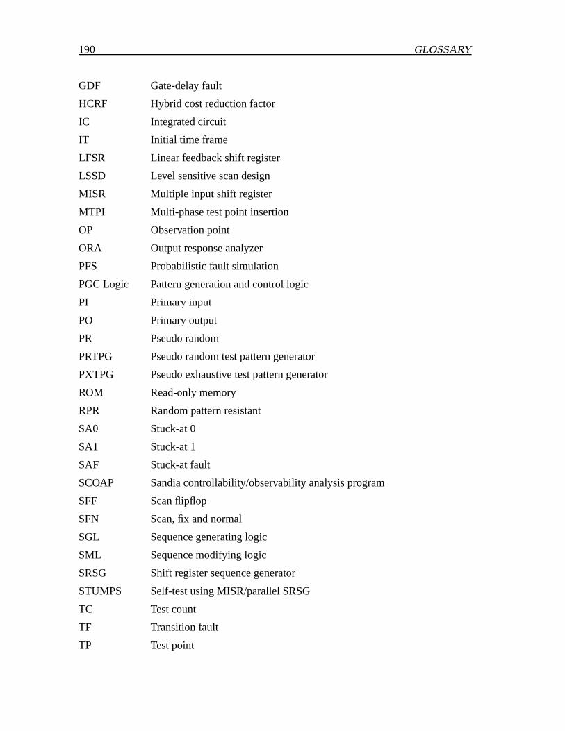
190 GLOSSARY
GDF Gate-delay fault
HCRF Hybrid cost reduction factor
IC Integrated circuit
IT Initial time frame
LFSR Linear feedback shift register
LSSD Level sensitive scan design
MISR Multiple input shift register
MTPI Multi-phase test point insertion
OP Observation point
ORA Output response analyzer
PFS Probabilistic fault simulation
PGC Logic Pattern generation and control logic
PI Primary input
PO Primary output
PR Pseudo random
PRTPG Pseudo random test pattern generator
PXTPG Pseudo exhaustive test pattern generator
ROM Read-only memory
RPR Random pattern resistant
SA0 Stuck-at 0
SA1 Stuck-at 1
SAF Stuck-at fault
SCOAP Sandia controllability/observability analysis program
SFF Scan flipflop
SFN Scan, fix and normal
SGL Sequence generating logic
SML Sequence modifying logic
SRSG Shift register sequence generator
STUMPS Self-test using MISR/parallel SRSG
TC Test count
TF Transition fault
TP Test point

GLOSSARY 191
TPG Test pattern generator
TPI Test point insertion
TSFF Transparent scan flipflop
XTPG Exhaustive test pattern generator
Symbols#CP Number of control points
#T P Number of test points
#WP Number of observation points
Φ Number of phases
φ Phase
C COP controllability
C0 COP 0-controllability
C1 COP 1-controllability
CM Cube mapping
CPmax Maximum number of control points
CU COP U-controllability
Cu Test cube
CZ COP Z-controllability
dK/dC Derivative of the cost with respect to a change in controllability
dK/dC0 Derivative of the cost with respect to a change in 0-controllability
dK/dC1 Derivative of the cost with respect to a change in 1-controllability
dK/dCZ Derivative of the cost with respect to a change in Z-controllability
dK/dE0 Derivative of the cost with respect to a change in essential zero counts
dK/dT 0 Derivative of the cost with respect to a change in total zero counts
dK/dT 1 Derivative of the cost with respect to a change in essential one counts
dK/dT 1 Derivative of the cost with respect to a change in total one counts
dK/dW Derivative of the cost with respect to a change in observability
dK/dWZ0 Derivative of the cost with respect to a change in Z↔0 observability
dK/dWZ1 Derivative of the cost with respect to a change in Z↔1 observability
E0 Essential zero count
E1 Essential one count

192 GLOSSARY
F Number of faults
f Fault
hr Feedback coefficient for memory cell r
iCu Image cube
IM Identity matrix
K Cost function
Km Cost of modified circuit, i.e., circuit with test points
L Number of signal lines
l Line
Mr Memory cell r
MBPC Minimum-benefit-per-cost
OPmax Maximum number of observation points
p Probability
Pd f COP detection probability of fault f
R Number of memory cells in a shift register
r Index of memory cells
SC0 SCOAP 0-controllability
SC1 SCOAP 1-controllability
sCu Source cube
SW SCOAP observability
T Number of test patterns
t Test pattern
T 0 Total zero count
T 1 Total one count
Tc Characteristic matrix
Tmin Minimum test set size
T Pmax Maximum number of test points
W COP observability
w Test pattern width
WZ0 COP Z↔0 observability
WZ1 COP Z↔1 observability
X(t) State/Pattern at time t

Bibliography
[Ake87] S.B. Akers, C. Joseph and B.Krishnamurthy. On the role of independent faultsets in the generation of minimal test sets. Proc. of the IEEE Int. Test Conf.,pages 1100–1107, 1987.
[Als94] M.F. Alshaibi and C.R. Kime. Fixed-biased pseudo-random built-in selft-testfor random pattern resistant circuits. Proc. of the IEEE Int. Test Conf., pages929–938, 1994.
[Bar87] P.H Bardell, W.H. McAnney and J. Savir. Built-In Pseudo-Random Testing ofDigital Circuits, chapter 8. John Wiley & Sons, New York, 1987.
[Bli89] Berkeley logic interchange format. http://www-cad.eecs.berkeley.edu/Res-pep/Research/sis/abstract.html, 1989.
[Bra84] R.K. Brayton, G.D. Hachtel C. McMullen, A. Sangiovanni-Vincentelli. LogicMinimization Algorithms for VLSI Synthesis. Kluwer Academic Publishers,Boston, 1984.
[Bra89] R.K. Brayton, Rudell R., A. Sangiovanni-Vincentelli, A.R.Wang. An exactminimizer for boolean relations. Proc. of IEEE Int. Conf. on Computer AidedDesign (ICCAD), pages 316–319, 1989.
[Brg84] F. Brglez. On testability analysis of combinational networks. Proc. of Int.Symp. on Circuits and Systems, pages 221–225, 1984.
[Brg85] F. Brglez and H. Fujiwara. A neural netlist of 10 combinational benchmarkdesigns and a special translator in fortran. Proc. of Int. Symp. on Circuits andSystems, June 1985.
[Brg89] F. Brglez et al. Combinational profiles of sequential benchmark circuits. Proc.of Int. Symp. on Circuits and Systems, pages 1929–1934, May 1989.
[Cha92] Jau-Shien Chang and Chen-Shang Lin. Test set compaction for combinationalcircuits. Proc. of Asian Test Symp., pages 20–25, November 1992.
193

194 BIBLIOGRAPHY
[Che95a] C. Chen, and S. Gupta. A methodology to design efficient bist test patterngenerators. Proc. of the IEEE Int. Test Conf., pages 814–823, 1995.
[Che95b] K-T. Cheng and C-J. Lin. Timing-driven test point insertion for full-scan andpartial-scan bist. Proc. of the IEEE Int. Test Conf., pages 506–514, 1995.
[Chr75] N. Christofedes and K. Korman. A computational survey of methods for theset covering problem. Management Science, 21(5):591–599, 1975.
[Duf91] C. Dufaza and G. Cambon. Lfsr based deterministic and pseudo-random testpattern generator structures. Proc. of European Test Conf., pages 27–34, 1991.
[Duf93] C. Dufaza and C. Chevalier. Lfsrom basic principle and bist application. Proc.of European Conf. on Design Automation, pages 211–216, 1993.
[Eic77] E.B. Eichelberger, and T.W. Williams. A logic design structure for lsi testabil-ity. Proc. of the 14th Design Automation Conf., pages 462–468, June 1977.
[Fei99] C. Feige, M.J. Geuzebroek, J. ten Pierick and H. Vranken. Lbist evaluationreport. Technical report, Philips Semiconductors B.V., December 1999.
[Fei01] C. Feige, and M.J. Geuzebroek. Logic bist technology evaluation: an industrialcase study. European Test Workshop - Informal Digest, pages 333–340, 2001.
[Fuj85] H. Fujiwara. Logic Testing and Design for Testability. The MIT Press, Cam-bridge, Massachusetts, 1985.
[Geu97a] M.J. Geuzebroek. The deterministic bist scheme. Master’s thesis, Delft Uni-versity of Technology, Faculty of Electrical Engineering, Mekelweg 4, 2628CD, Delft, April 1997.
[Geu97b] M.J. Geuzebroek. Test point insertion techniques. Technical Report 1-68340-44(1997)13, Delft University of Technology, Faculty of Electrical Engineering,Mekelweg 4, 2628 CD, Delft, November 1997.
[Geu00] M.J. Geuzebroek, J.Th. van der Linden and A.J. van de Goor. Test point inser-tion for compact test sets. Proc. of the IEEE Int. Test Conf., pages 292–301,2000.
[Geu01] M.J. Geuzebroek, A.J. van de Goor and J.Th. van der Linden. Facilitating au-tomatic test pattern generators using test point insertion. World Market SeriesBusiness Briefing: Global Semiconductor Manufacturing Technology, pages149–152, Januari 2001.
[Geu02a] M.J. Geuzebroek. Tpi facilitation techniques. Technical report, Delft Univer-sity of Technology, Faculty of Electrical Engineering, Mekelweg 4, 2628 CD,Delft, November 2002.

BIBLIOGRAPHY 195
[Geu02b] M.J. Geuzebroek, J.Th. van der Linden and A.J. van de Goor. Test point in-sertion that facilitates atpg in reducing test time and data volume. Proc. of theIEEE Int. Test Conf., pages 138–147, 2002.
[Geu03] M.J. Geuzebroek, A.J. van de Goor and J.Th. van der Linden. Tpi for im-proving pr fault coverage of boolean and three-state circuits. To appear at theEuropean Test Workshop 2003, pages xx–xx(6 pages), 2003.
[Glo93] C. Gloster. Dynamic scan testing: Investigating a new paradigm. Tech-nical report, MCNC, Center of Mictroelectronics, 1993. INTERNET:http://www.cbl.ncsu.edu/pub/Benchmark dirs/ISCAS89/ADDENDUM93/DOCUMENTATION/main.ps.
[Goe81] P. Goel, and B.C. Rosales. Podem-x: An automatic test generation system forvlsi logic circuits. Proc. of 18th Design Automation Conf., pages 260–268,1981.
[Gol80] L.H. Goldstein and E.L. Thigpen. Scoap: Sandia controllability/observabilityanalysis program. Proc. of 17th Design Automation Conf., pages 190–196,1980.
[Gu 01] X. Gu , S.S. Chung, F. Tsang, J.A. Tofte and H. Rahmanian. An effor-minimized logic bist implementation method. Proc. of the IEEE Int. Test Conf.,pages 1002–1010, 2001.
[Hap93] F. Hapke and R. Reche. Amsal reference manual. Technical Report Release01.08.00, Philips GmbH, VALCO RHW, Stresemannallee 101, D-2000 Ham-burg 54, Germany, September 1993.
[Har93] J. Hartmann, and G. Kemnitz. How to do weighted random testing for bist.Proc. of IEEE Int. Conf. on Computer Aided Design (ICCAD), pages 568–571,1993.
[Hay74] J.P. Hayes and A.D. Friedman. Test point placement to simplify fault detection.IEEE Transactions on Computers, C-33:727–735, July 1974.
[Hel92] S. Hellebrand, S. Tarnick, J. Rajski and B. Courtois. Generation of vector pat-terns through reseeding of multiple-polynomial linear feedback shift registers.Proc. of the IEEE Int. Test Conf., pages 120–129, 1992.
[Het99] G. Hetherington, T. Fryars, N. Tamarapalli, M. Kassab, A. Hassan and J. Ra-jski. Logic bist for large industrial designs: Real issues and case studies. Proc.of the IEEE Int. Test Conf., pages 358–367, 1999.
[Hor89] P.D. Hortensius, R.D. McLeod, W. Pries, D.M. Miller and H.C. Card. Cellularautomata-based pseudorandom number generators for built-in-self-test. IEEETransactions on Computer-Aided Design, 8(8):842–859, 1989.

196 BIBLIOGRAPHY
[Kag96] D. Kagaris, S. Tragoudas and A. Majumdar. Deterministic test pattern repro-duction by a counter. Proc. of European Design and Test Conf., pages 37–41,1996.
[Kie98] G. Kiefer and H-J. Wunderlich. Deterministic bist with multiple scan chains.Proc. of the IEEE Int. Test Conf., pages 1057–1064, 1998.
[Kie00] G. Kiefer, H. Vranken, E.J. Marinissen and H-J. Wunderlich. Application ofdeterministic logic bist on industrial circuits. Proc. of the IEEE Int. Test Conf.,pages 105–114, 2000.
[Kis89] Logic synthesis and optimization benchmarks.http://www.cbl.ncsu.edu/pub/Benchmark dirs/LGSynth89/DOCUMEN-TATION, 1989.
[Kon96a] M.H. Konijnenburg and J.Th. van der Linden. Data structures and algorthimsof the delft automatic test pattern generation system (dat). Technical Report 1-68340-44(1996)06, Delft University of Technology (Faculty of Electrical En-gineering, Department CARDIT), Mekelweg 4, 2628 CD Delft, March 1996.
[Kon96b] M.H. Konijnenburg and J.Th. van der Linden. Delft Automatic Test PatternGeneration Platform (DAT) User Manual. Delft University of Technology(Faculty of Electrical Engineering, Department CARDIT), Mekelweg 4, 2628CD Delft, March 1996.
[Kon96c] M.H. Konijnenburg, J.Th. van der Linden and A.J. van de Goor. Acceleratedcompact test set generation for three-state circuits. Proc. of the IEEE Int. TestConf., pages 29–38, October 1996.
[Kon98] M.H. Konijnenburg. Automatic Test Pattern Generation for Synchronous Se-quential Circuits. PhD thesis, Delft University of Technology, Faculty of Elec-trical Engineering, Mekelweg 4, 2628 CD, Delft, December 1998.
[Kri87] B. Krishnamurthy. A dynamic programming approach to the test point in-sertion problem. Proc. of 24th ACM/IEEE Design Automation Conf., pages695–705, 1987.
[Lem94] M. Lempel, S.K. Gupta and M. Breuer. Test embedding with discrete loga-rithms. Proc. of 12th IEEE VLSI Test Symposium, pages 74–80, 1994.
[Lis87] R. Lisanke, F. Brglez, A.J. Degeus and D. Gregory. Testability-driven randomtest-pattern generation. IEEE Transactions on Computer-Aided Design, CAD-6:1082–1087, 1987.
[Maj94] A. Majumdar. A new procedure for weighted random built-in self-test. Proc.of IEEE Int. Conf. on Computer Aided Design (ICCAD), pages 288–291, 1994.

BIBLIOGRAPHY 197
[Mur90] F. Muradali, V.K. Argarwal and B. Nadeau-Dostie. New procedure forweighted random built-in-self-test. Proc. of the IEEE Int. Test Conf., pages660–669, 1990.
[Nag95] P. Nagvajara and P. Kumhon. Built-in self-test based on pre-stored test. PrivateCommunication, Drexel University Philadelphia, 1995.
[Nak99] M. Nakao, S. Kobayashi, K. Hatayama, K. Iijima and S. Terada. Low overheadtest point insertion for scan-based bist. Proc. of the IEEE Int. Test Conf., pages348–357, 1999.
[Pat91] S. Pateras and J. Rajski. Generation of correlated random patterns for thecomplete testing of synthesized multi-level circuits. Proc. of 28th ACM/IEEEDesign Autom. Conf., pages 347–352, 1991.
[Poh78] S.C. Pohlig and M. Hellman. An improved algorithm for computing logarithmsover gf(p) and its cryptographic significance. IEEE Trans. Information Theory,IT-24(1):106–110, 1978.
[Pom91] I. Pomeranz, L.N. Reddy and S.M. Reddy. Compactest: A method to generatecompact test sets for combinational circuits. Proc. of the IEEE Int. Test Conf.,pages 194–203, 1991.
[Pom93] I. Pomeranz and S.M. Reddy. 3-weight pseudo-random test generation basedon a deterministic test set for combinational and sequential circuits. IEEETransactions on Computer-Aided Design, 12(7):1050–1058, 1993.
[Pra95] G. Pramadono. Dat’s path delay fault atpg. Master’s thesis, Delft University ofTechnology, Faculty of Electrical Engineering, Mekelweg 4, 2628 CD, Delft,August 1995.
[Raj99] J. Rajski, G. Mrgugalski and J. Tyszer. Comparison study of ca-based prpgsand lfsrs with phase shifters. Proc. of 17th IEEE VLSI Test Symposium, pages236–245, 1999.
[Ree96] B. Reeb and H-J. Wunderlich. Deterministic pattern generation for weightedrandom pattern testing. Proc. of European Test Conf., pages 30–36, March1996.
[Sav91] Y. Savaria, M. Youssef, B. Kaminska and M. Koudil. Automatic test point in-sertion for pseudo-random testing. Proc. of International Symposium on Cir-cuits and Systems, pages 1960–1963, 1991.
[Sch95] C. Schotten and H. Meyr. Test point insertion for an area efficient bist. Proc.of the IEEE Int. Test Conf., pages 515–523, 1995.

198 BIBLIOGRAPHY
[Sei91] B.H. Seiss, P.M. Trouborst and M.H. Schulz. Test point insertion for scan-based bist. Proc. of 2nd European Test Conf., pages 253–262, 1991.
[Sem01] Semiconductor Industry Association. International technologyroadmap for semi-conductors 2001 edition, test and test equipment.http://public.itrs.net/Files/2001ITRS/Test.pdf, 2001.
[Sen92] E. Sentovich, K. Singh, C. Moon, H. Savoj, R. Brayton and A. Sangiovanni-Vincentelli. Sequential circuit design using synthesis and optimization. Proc.of Int. Conf. on Computer Design, pages 328–333, 1992.
[Smi85] G.L. Smith. Model for delay faults based upon paths. Proc. of the IEEE Int.Test Conf., pages 342–349, 1985.
[Tam96] N. Tamarapalli and J. Rajski. Constructive multi-phase test point insertion forscan-based bist. Proc. of the IEEE Int. Test Conf., pages 649–658, 1996.
[Tou95] N.A. Touba and E.J. McCluskey. Transformed pseudo-random patterns forbist. Proc. of 13th IEEE VLSI Test Symposium, pages 410–416, 1995.
[Tou96] N.A. Touba and E.J. McCluskey. Test point insertion based on path tracing.Proc. of 14th IEEE VLSI Test Symposium, pages 2–8, 1996.
[Tro91] Gert-Jan Tromp. Minimal test sets for combinational circuits. Proc. of theIEEE Int. Test Conf., pages 204–209, 1991.
[Tsa97] H.-C. Tsai, K.-T. Cheng, C.-J. Lin and S. Bhawmik. A hybrid algorithm fortest point selection for scan-based bist. Proc. of 34th Design Automation Conf.,pages 478–483, 1997.
[Vas93] B. Vasudevan, D.E. Ross, M. Gala and K.L. Watson. Lfsr based deterministichardware for at-speed bist. Proc. of 11th IEEE VLSI Test Symposium, pages201–207, 1993.
[vdG98] A.J. van de Goor. Testing Semiconductor Memories, Theory and Practice.ComTex Publishing, http://cardit.et.tudelft.nl/˜vdgoor, 1998.
[vdL96] J. Th. van der Linden. Automatic Test Pattern Generation for Three-State Cir-cuits. PhD thesis, Delft University of Technology, Faculty of Electrical Engi-neering, Mekelweg 4, 2628 CD, Delft, May 1996.
[Vra02] H. Vranken, F. Meister and H-J. Wunderlich. Combining deterministic logicbist with test point insertion. Proc. of the Seventh IEEE European Test Work-shop, pages 105–110, 2002.
[Wai89] J.A. Waicukauski, E. Lindblook, E.B. Eichelberger and O.P. Forlenza. Amethod for generating weighted random test patterns. IBM J. Res. Develop.,33(2):149–161, March 1989.

BIBLIOGRAPHY 199
[Wai90] J.A. Waicukauski, P.A.Shupe, D.J. Giramma and A. Matin. Atpg for ultra-largestructured designs. Proc. of the IEEE Int. Test Conf., pages 44–51, 1990.
[Wil81] T.W. Williams, and N.C. Brown. Defect level as function of fault coverage.IEEE Transactions on Computers, C-030:987–988, 1981.
[Wun96] H.-J. Wunderlich and G. Kiefer. Bit-flipping bist. Proc. of IEEE Int. Conf. onComputer Aided Design (ICCAD), pages 337–343, 1996.
[You93] M. Youssef, Y. Savaria and B. Kaminska. Methodology for efficiently insertingand condensing test points. IEEE Proceedings-E, 140(3):154–160, 1993.

200 BIBLIOGRAPHY

Samenvatting (Summary in Dutch)
Test punt toevoeging voor het verbeteren van BIST prestaties, en hetreduceren van ATPG test tijd en data volume
Dit proefschrift behandelt het vergemakkelen van structureel testen van geıntegreerdecircuits (chips) op mogelijke defecten. Tijdens het fabricage-proces van chips, kunnendefecten optreden, zoals extra of ontbrekende verbindingen door stofdeeltjes, waardoorde chips niet meer volgens verwachting werken. Om te voorkomen dat chips met defectentoch in consumenten producten terechtkomen, worden structurele testen uitgevoerd doortesters. Echter, door de steeds toenemende complexiteit van chips, worden de kosten vandeze testers steeds hoger. Moore’s law dicteert dat de snelheid (klokfrequentie) en degeheugencapaciteit van de testers steeds groter moet worden. Deze steeds grotere testerkosten gaan een steeds belangrijker aandeel vormen in de prijzen van chips.
Een alternatief voor het uitvoeren van de tests door externe testers is het insluiten vande test op de chip zelf, Built-In Self-Test (BIST) genaamd. Hierdoor is er geen snelletester met heel veel geheugen meer vereist, maar kan de chip ook door een veel goed-kopere (tragere en met minder geheugen toegeruste) tester worden gestart. De chip hoeftalleen maar aangestuurd worden om zichzelf te testen en na de test behoeft alleen maar’gevraagd’ te worden of de chip defecten bezit.
In Hoofdstuk 2 worden verscheidene bestaande BIST methodes beschreven en gecat-egoriseerd, waarbij wordt gekeken naar de foutdekking, extra silicium oppervlak en debruikbaarheid op grote industriele chips.
Een belangrijk nadeel van BIST is dat bij moeilijk testbare circuits, of de foutdekkingvaak een stuk lager is dan bij het extern testen, of de extra benodigde chip oppervlak tegroot is. Een manier om de testbaarheid van chips te verbeteren is Test Punt Toevoeging(Test Point Insertion (TPI)), waardoor de foutdekking bij BIST verbetert en ook de ben-odigde extra chip oppervlak afneemt. Hoofdstuk 3 beschrijft de algemene werking vanTPI en verdeelt de methodes die gebruikt worden voor het bepalen van de posities van detest punten (TPs), in categorieen. Niet elk circuit, of elke positie op de chip, is geschiktvoor een TP. In de industrie komen naast Boolean elementen ook vaak circuits met ’three-state’ elementen voor. Deze geven nog meer restricties. In Hoofdstuk 3 wordt ook eenbeschrijving gegeven van bestaande TPI algoritmes. Ook wordt een overzicht gegevenvan de TPI onderwerpen in de hoofdstukken 4 tot 6 en de circuits die zijn gebruikt voorhet testen van de TPI algoritmes.
Hoofdstuk 4 begint met het selecteren van een bestaand TPI algoritme voor verdere
201

202 Samenvatting (Summary in Dutch)
ontwikkeling. Een nadeel van dit algoritme is dat het is ontworpen voor Boolean circuitsen niet voor industriele circuits. Dit algoritme wordt aangepast voor complexe industrielecircuits. Daarnaast wordt het TPI algoritme ook aangepast voor een nog grotere fout-dekking na TPI, en wordt een methode gepresenteerd waarmee de processor tijd gebruiktdoor TPI, significant wordt gereduceerd, zonder dat de kwaliteit van de gekozen TP posi-ties negatief wordt beınvloed.
De tests voor op de testers worden gegenereerd door Automatische Test Patroon Gen-erators (ATPGs). TPI zorgt niet alleen voor een hogere foutdekking bij BIST, doch ookvoor kleinere ATPG test sets, omdat het makkelijker wordt om voor de te dekken foutentest patronen te genereren. Hierdoor wordt het ook makkelijker om meerdere fouten telaten dekken door een test patroon en daardoor het totaal aantal testpatronen te verkleinen.In Hoofdstuk 5 wordt aangetoond dat het BIST TPI algoritme voor industriele circuits,gepresenteerd in Hoofdstuk 4, al goed in staat is de test sets flink te verkleinen, waarbijtevens de foutdekking toeneemt en de ATPG processor tijd nodig om de tests te gener-eren fors afneemt. Echter niet voor alle circuits wordt een even goede reductie van hetaantal test patronen gehaald. Er zijn specifieke ATPG gerelateerde test problemen die hetTPI algoritme niet weet op te lossen. In Hoofdstuk 5 wordt beschreven hoe test counts(TCs), die een schatting geven voor de minimale grootte van de test, in het TPI algoritmekunnen worden geıntegreerd om de grootte van de ATPG test sets nog meer te verkleinen.Een ander probleem voor de ATPG zijn zeer grote fan-out vrije gebieden in de circuits.Deze zorgen vaak voor grote test sets en moeten daardoor gedurende TPI verkleind wor-den. Hiervoor worden vier methoden gepresenteerd die gebruikt kunnen worden voor hetverkleinen van deze fan-out vrije gebieden. Omdat elk circuit zijn eigen specifieke testproblemen heeft, wordt een nieuwe TPI algoritme gepresenteerd dat bestaat uit meerderestadia. In elke stadium wordt eerst uitgezocht welk test probleem of problemen het belan-grijkst zijn om te worden aangepakt. Het TPI algoritme zal dan enkele TPs toevoegen omdit test probleem aan te pakken. In het volgende stadium wordt opnieuw bekeken welktest probleem het belangrijkst is om aan te pakken. Resultaten in Hoofdstuk 5 laten ziendat hiermee het aantal test patronen nog verder gereduceerd kan worden.
In Hoofdstuk 6 wordt aangetoond dat TPI niet alleen werkt voor het vergemakkelenen verkleinen van ATPG test sets voor het stuck-at fault (SAF) foutmodel, maar ook voorhet gate-delay fault (GDF) model. De GDF test sets zijn vaak nog groter dan de SAFtest sets, waardoor TPI ook voor dit foutmodel een belangrijke rol kan spelen. Uit de re-sultaten blijkt dat niet alleen het aantal GDF test patronen significant afneemt, maar ookdat de foutdekking behoorlijk toeneemt na TPI. Ook de processor tijd voor GDF ATPGneemt fors af.
Tot slot wordt in Hoofdstuk 7 een samenvatting gegeven van het onderzoek, wordende belangrijkste bijdrages opgesomd en worden aanbevelingen gedaan voor verder onder-zoek.
Jeroen Geuzebroek
Curriculum Vitae
Jeroen Geuzebroek was born in Rotterdam on June 18, 1974. After his secondaryeducation at the R.S.G. (currently “Maerlant College”) in Brielle from 1986 to 1992, hestudied at the department of Electrical Engineering of the Delft University of Technology,where he graduated in 1997. During his masters study, he investigated the advantagesand disadvantages of state-of-the-art BIST implementations, i.e., BIST implementationsthat embed deterministic test patterns. One deterministic BIST method, the Determin-istic LFSR was implemented in the DAT test tool, developed at the Delft University ofTechnology. In 1997 he started this PhD study at the computer architecture group ofProf. A.J. van de Goor. This research was funded by Philips Semiconductors. The soft-ware developed during this research has been integrated in Philips’ production test systemworldwide. During his PhD period, Jeroen also joined Philips for several months for theevaluation of a BIST tool. Jeroen’s (research) interests include Design-for-Test, all aspectsof facilitating testing, especially with respect to test data reduction and compression, andthe development of software for solving complex problems.
203

204 Curriculum Vitae