test circuits for 3-d systems integration - electrical and computer
TRANSCRIPT

Test Circuits for 3-D Systems Integration
Ioannis Savidis and Eby G. FriedmanDepartment of Electrical and Computer Engineering
University of RochesterRochester, NY 14627
[email protected], [email protected]
Abstract— Three test circuits have been developed to ex-perimentally demonstrate and stress the state-of-the-art in 3-D integrated systems. Several critical elements of this emerg-ing technology, synchronization, power delivery, and thermalmanagement, are just beginning to be explored. The three testcircuits explore these three fundamental design issues. The firsttest circuit examines multi-plane synchronization for a stackedsystem of three device planes. Experimental data compare skew,slew, and power consumption for different network topologies.The second test circuit examines power delivery in a threeplane 3-D system. The noise propagation characteristics withinthe power and ground networks are experimentally assessedby varying the through-silicon via (TSV) density and usingdedicated planes. The third 3-D circuit includes five CMOSplanes, two logic planes and three memory planes, and includesmultiple circuits that examine a range of 3-D design issues.The test structures are designed to evaluate thermal couplingbetween CMOS device planes and decoupling capacitance in3-D power delivery networks. These test circuits are discussed,and trends and challenges are outlined.
Index Terms— 3-D integration, clock distribution, noisepropagation, power distribution, thermal coupling, decouplingcapacitor placement.
I. INTRODUCTION
Three of the most omnipresent and challenging issues inhigh performance 3-D systems are synchronization, powerdelivery, and thermal management. The interdependence ofthese issues is of critical importance in 3-D systems, as noiseon the power network can adversely affect the clock network,current loads can produce severe hot spots within a 3-Dstack, and the location of the hot spots can adversely affectmultiplane synchronization. Enhanced understanding of theseinterrelated 3-D design challenges is therefore necessary todevelop design techniques and methodologies to effectivelydeliver clock and power while managing thermal effects.
Each of these three individual topics is examined inde-pendently through three recent test circuits. The first testcircuit examines the effects of the clock delivery topologyon the clock skew at the leafs of each device plane andis shown in Fig. 1a. The second test circuit focuses onpower delivery in 3-D integrated systems. The objective ofthis test circuit is to provide a quantitative analysis of the
This research is supported in part by the National Science Foundationunder Grant Nos. CCF-0811317 and CCF-0829915, grants from the NewYork State Office of Science, Technology and Academic Research tothe Center for Advanced Technology in Electronic Imaging Systems, andby grants from Intel Corporation, Qualcomm Corporation, and SamsungElectronics.
noise characteristics of each plane within a three plane 3-D integrated system. A microphotograph of the second testcircuit is shown in Fig. 1b. The third test circuit has beendesigned to examine cross-plane thermal coupling betweenadjacent device planes. Thermal effects can potentially alterthe performance of the clock and power networks due to hotspots. A microphotograph of the third test circuit is shownin Fig. 1c.
In the following section, the test circuit examining clockdelivery in 3-D systems is discussed. This section is followedby a discussion of the 3-D power delivery test circuit inSection III. A description of the third test circuit examin-ing cross-plane thermal coupling and decoupling capacitorplacement is provided in Section IV. Some conclusions areoffered in Section V.
II. CLOCK DISTRIBUTION IN 3-D SYSTEMS
The reliable distribution of the clock signal to the manyhundreds of thousands of sequential elements distributedthroughout a synchronous circuit [1], [2] is further exacer-bated in 3-D ICs as sequential elements belonging to thesame clock domain can be located on multiple planes. In 2-Dcircuits, symmetric interconnect structures are widely used todistribute the clock signal across a circuit [2], permitting theclock signal to arrive at the leaves of the tree at approximatelythe same time. Maintaining this symmetry within a 3-Dcircuit, however, is a difficult task. This first test circuiton multiplane synchronization has provided insight into thebenefits and challenges of asymmetric clock structures in 3-Dcircuits.
Three topologies to globally distribute a clock signalwithin a 3-D circuit have been evaluated. A 3-D test circuit,based on the MITLL 180 nm CMOS 3-D manufacturingprocess with 1.75 µm diameter TSVs [3], is experimentallydemonstrated to operate at 1.4 GHz [4].
The test circuit consists of three blocks. Each blockincludes the same logic circuit but implements a differentclock distribution topology. The total area of the test circuitis 3 mm × 3 mm, where each block occupies an approximatearea of 1 mm2. Each block contains about 30,000 transistorswith a power supply voltage of 1.5 volts. The different clockdistribution topologies are reviewed in Section II-A, andexperimental results are discussed in Section II-B.
A. 3-D clock topologies
Several clock network topologies for 3-D ICs are describedin this section. These topologies are commonplace in 2-D
181

(a) (b) (c)Fig. 1. Microphotograph of the test circuits investigating a) clock distribution, b) power delivery, and c) thermal coupling in 3-D circuits.
1st plane
2 nd plane
3rd plane
1st plane
2 nd plane
3rd plane
Local clnetwork
1st plane
2 nd plane
3rd plane
(a) (b)
(c)
TCC TCC
TCC
TCB
TCB
TCB
TCA
TCA TCA
Fig. 2. Three 3-D clock distribution networks within the test circuit, (a)H-trees, (b) H-tree and local rings, and (c) H-tree and global rings.
circuits, such as H-trees, rings, and meshes [2]. Each of thethree blocks includes a different clock distribution structure,which is schematically illustrated in Fig. 2. The dashedlines depict vertical interconnects implemented by groupsof through silicon vias. Multiple TSVs at the connectionpoints between the clock networks lower the resistance ofthe vertical path while enhancing reliability.
A primary objective is to evaluate the effects of the TSVson clock skew. Load balancing the global rings is shownto reduce the delay of the clock signal due to the TSVs.Local meshes are preferable since the distribution of the clocksignal to the sinks is limited within a physical plane. Stacks ofTSVs connect the sinks on other planes through local rings.This topology offers the advantage of limiting most of theclock paths within one physical plane, while distributing thesignal vertically to localized areas within neighboring planes.
The effects that these topological choices have on the clockskew are experimentally described in Table I. Equidistantsignal propagation in a 3-D system is complicated by the dif-ferent impedance characteristics of the vertical and horizontalinterconnects. Consequently, the objective is to provide aglobal clock topology that produces sufficiently low skew (or
TABLE ICLOCK SKEW AMONG THE PLANES OF EACH BLOCK AND THE AVERAGE
POWER CONSUMED BY EACH TOPOLOGY.
Clock Averagedistribution power Clock skew Frequency (MHz)
network (mW) (ps) 10 40 160 500 1000
tBA = | tB − tA | 59.0 59.7 — 18.7 26.2H-tree 260.5 tBC = | tB − tC | 66.8 88.5 — 20.1 30.2
(Fig. 2a) tAC = | tA − tC | 7.8 28.8 — 1.4 4.1tBA = | tB − tA | 122.5 82.3 70.0 159.1 112.1
Local rings 228.5 tBC = | tB − tC | 70.8 48.9 38.0 144.5 131.1(Fig. 2b) tAC = | tA − tC | 51.7 33.4 32.0 14.5 19.1
tBA = | tB − tA | — 23.6 30.4 — 68.3Global rings 168.3 tBC = | tB − tC | — 38.2 42.2 — 18.6
(Fig. 2c) tAC = | tA − tC | — 14.6 11.8 — 49.7
predictable skew for delay compensation) within (intra-plane)and among (inter-plane) the planes of a 3-D circuit. Thesymmetry of an H-tree and the load balancing characteristicsof the rings and meshes are exploited. The power consumedby each 3-D clock architecture is also considered due to theimportance of thermal issues in 3-D circuits.
B. Experimental results
The clock skew between the planes of each block is listedin Table I. The difference in the arrival time of the clocksignal between planes i and j is denoted as ti j, and representsthe clock skew between these two locations. The averagepower consumed by the buffers for each clock distributiontopology is also listed in Table I.
The clock skew measurements indicate that a topologycombining the symmetry of an H-tree on the second planeand global rings on the remaining two planes results inlow clock skew in 3-D circuits while consuming a mod-erate amount of power. This structure, however, producesthe greatest root to leaf clock delay as compared to theother topologies. Alternatively, for the H-tree and local ringstopologies, the lowest power is consumed.
III. POWER DELIVERY FOR STACKED TECHNOLOGIES
Power distribution networks for 3-D systems are naturallymore complex than a two-dimensional power network. Inaddition, power delivery in 3-D integrated systems presentsdifficult new challenges for delivering sufficient current toeach device plane [5], while leading to high power densities
182

[6]. Specialized techniques are therefore required to ensurethat each device plane is operational, while not exceeding atarget output impedance [7]. The IR voltage drops and L·di/dtswitching noise are affected by the density and electricalcharacteristics of the TSVs [8]. A comparison of two differentvia densities for identical power distribution networks ispresented, and the effects of the 3-D via density on the powernetwork design process are discussed.
The fabricated test circuit is 2 mm × 2 mm, and composedof four equal area quadrants (see Fig. 1b). Three quadrantsare used to evaluate the effects of the power distributionnetwork topology on the noise propagation characteristics,and one quadrant is dedicated to DC-to-DC conversion.Each stacked power network is 530 µm x 500 µm, andincludes three discrete two-dimensional power networks, onenetwork on each of the three device planes. The total areaoccupied by each block is less than 0.3 mm2, representing aportion of a power delivery network. Each block includes thesame logic circuit but utilizes a different power distributionarchitecture. The power supply voltage is 1.5 volts for allof the blocks. The third MITLL 3-D multi-project waferincludes 1.25 µm diameter TSVs, and CMOS devices withchannel lengths of 150 nm. The different power distributiontopologies are reviewed in Section III-A, and experimentalresults are provided in Section III-B.
A. 3-D power topologies
Three topologies to distribute power within a 3-D circuithave been designed and manufactured, and an analysis ofthe peak noise voltage, voltage range, and average noise forthe power and ground network is described. Interdigitatedpower/ground lines are used in all of the topologies. Thefour main objectives for the test circuit are to i) determinethe peak and average noise within the power and grounddistribution networks, ii) determine the effects of the boardlevel decoupling capacitors on reducing undesired noise, iii)explore the effects of a dedicated power/ground plane onthe power noise, and iv) investigate the effects of the TSVdensity on the noise characteristics of the power network. Thethree power network topologies are illustrated in Fig. 3. Thedifference between the left (Block 1) and central (Block 2)topologies is the number of TSVs, where the latter topologycontains 50% more TSVs. The third topology (Block 3)replaces the interdigitated power and ground lines on thesecond device plane with two metal planes to evaluate thebenefit of dedicated power and ground planes on deliveringcurrent within a 3-D system.
B. Experimental results
The peak noise for each topology, with or without aboard level decoupling capacitance, is shown in Fig. 4. Nosingle topology contributes the largest noise voltage at anyspecific bias voltage. The average noise for each topologyis approximately 75% to 90% lower than the peak-to-peakvoltage, indicating that a majority of the data is located withinclose proximity of the nominal power and ground voltages.
Fig. 3. Power distribution network topologies. (a) interdigitated powernetwork on all planes with the 3-D vias distributing current on the peripheryand through the middle of the circuit, (b) interdigitated power network onall planes with the 3-D vias distributing current on the periphery, and (c)interdigitated power network on planes 1 and 3 and power/ground planes onplane 2 with the 3-D vias distributing current on the periphery and throughthe middle of the circuit.
0 0.25 0.5 0.75 1 1.2560
80
100
120
140
160
180
200
220
240
Bias voltage (V)
Pea
k n
ois
e a
mp
litu
de (
mV
)
Block 1Block 2Block 3
0 0.25 0.5 0.75 1 1.2540
45
50
55
60
65
70
75
80
85
Bias voltage (V)
Pea
k n
ois
e a
mp
litu
de (
mV
)
Block 1Block 2Block 3
(a) (b)
0 0.25 0.5 0.75 1 1.2555
60
65
70
75
80
85
Bias voltage (V)
Peak n
ois
e a
mp
litu
de (
mV
)
Block 1Block 2Block 3
0 0.25 0.5 0.75 1 1.2515
20
25
30
35
40
45
50
Bias voltage (V)
Peak n
ois
e a
mp
litu
de (
mV
)
Block 1Block 2Block 3
(c) (d)
Fig. 4. Peak noise voltage on the power and ground distribution networkswith and without board level decoupling capacitance. (a) peak noise ofpower network without decoupling capacitance, (b) peak noise of powernetwork with decoupling capacitance, (c) peak noise of ground networkwithout decoupling capacitance, and (d) peak noise of ground network withdecoupling capacitance.
In addition, the saturation voltage of the detection circuitry atthe output node (port0) is approximately 230 mV when thegain is -4.2 dB. The noise detection range is approximately600 mV centered around 1.5 volts and 0 volts, respectively,for the power and ground lines. The detection circuits forthe power network, therefore, detect noise that ranges from1.2 volts to 1.8 volts, and for the ground networks from -0.3volts to 0.3 volts.
183
High resistanceheaters
Four point resistance measurements
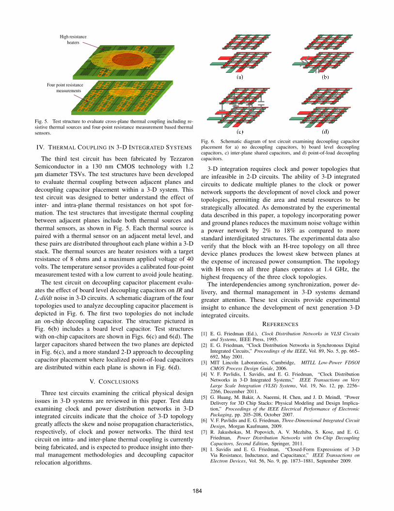
Fig. 5. Test structure to evaluate cross-plane thermal coupling including re-sistive thermal sources and four-point resistance measurement based thermalsensors.
IV. THERMAL COUPLING IN 3-D INTEGRATED SYSTEMS
The third test circuit has been fabricated by TezzaronSemiconductor in a 130 nm CMOS technology with 1.2µm diameter TSVs. The test structures have been developedto evaluate thermal coupling between adjacent planes anddecoupling capacitor placement within a 3-D system. Thistest circuit was designed to better understand the effect ofinter- and intra-plane thermal resistances on hot spot for-mation. The test structures that investigate thermal couplingbetween adjacent planes include both thermal sources andthermal sensors, as shown in Fig. 5. Each thermal source ispaired with a thermal sensor on an adjacent metal level, andthese pairs are distributed throughout each plane within a 3-Dstack. The thermal sources are heater resistors with a targetresistance of 8 ohms and a maximum applied voltage of 40volts. The temperature sensor provides a calibrated four-pointmeasurement tested with a low current to avoid joule heating.
The test circuit on decoupling capacitor placement evalu-ates the effect of board level decoupling capacitors on IR andL·di/dt noise in 3-D circuits. A schematic diagram of the fourtopologies used to analyze decoupling capacitor placement isdepicted in Fig. 6. The first two topologies do not includean on-chip decoupling capacitor. The structure pictured inFig. 6(b) includes a board level capacitor. Test structureswith on-chip capacitors are shown in Figs. 6(c) and 6(d). Thelarger capacitors shared between the two planes are depictedin Fig. 6(c), and a more standard 2-D approach to decouplingcapacitor placement where localized point-of-load capacitorsare distributed within each plane is shown in Fig. 6(d).
V. CONCLUSIONS
Three test circuits examining the critical physical designissues in 3-D systems are reviewed in this paper. Test dataexamining clock and power distribution networks in 3-Dintegrated circuits indicate that the choice of 3-D topologygreatly affects the skew and noise propagation characteristics,respectively, of clock and power networks. The third testcircuit on intra- and inter-plane thermal coupling is currentlybeing fabricated, and is expected to produce insight into ther-mal management methodologies and decoupling capacitorrelocation algorithms.
Fig. 6. Schematic diagram of test circuit examining decoupling capacitorplacement for a) no decoupling capacitors, b) board level decouplingcapacitors, c) inter-plane shared capacitors, and d) point-of-load decouplingcapacitors.
3-D integration requires clock and power topologies thatare infeasible in 2-D circuits. The ability of 3-D integratedcircuits to dedicate multiple planes to the clock or powernetwork supports the development of novel clock and powertopologies, permitting die area and metal resources to bestrategically allocated. As demonstrated by the experimentaldata described in this paper, a topology incorporating powerand ground planes reduces the maximum noise voltage withina power network by 2% to 18% as compared to morestandard interdigitated structures. The experimental data alsoverify that the block with an H-tree topology on all threedevice planes produces the lowest skew between planes atthe expense of increased power consumption. The topologywith H-trees on all three planes operates at 1.4 GHz, thehighest frequency of the three clock topologies.
The interdependencies among synchronization, power de-livery, and thermal management in 3-D systems demandgreater attention. These test circuits provide experimentalinsight to enhance the development of next generation 3-Dintegrated circuits.
REFERENCES
[1] E. G. Friedman (Ed.), Clock Distribution Networks in VLSI Circuitsand Systems, IEEE Press, 1995.
[2] E. G. Friedman, “Clock Distribution Networks in Synchronous DigitalIntegrated Circuits,” Proceedings of the IEEE, Vol. 89, No. 5, pp. 665–692, May 2001.
[3] MIT Lincoln Laboratories, Cambridge, MITLL Low-Power FDSOICMOS Process Design Guide, 2006.
[4] V. F. Pavlidis, I. Savidis, and E. G. Friedman, “Clock DistributionNetworks in 3-D Integrated Systems,” IEEE Transactions on VeryLarge Scale Integration (VLSI) Systems, Vol. 19, No. 12, pp. 2256–2266, December 2011.
[5] G. Huang, M. Bakir, A. Naeemi, H. Chen, and J. D. Meindl, “PowerDelivery for 3D Chip Stacks: Physical Modeling and Design Implica-tion,” Proceedings of the IEEE Electrical Performance of ElectronicPackaging, pp. 205–208, October 2007.
[6] V. F. Pavlidis and E. G. Friedman, Three-Dimensional Integrated CircuitDesign, Morgan Kaufmann, 2009.
[7] R. Jakushokas, M. Popovich, A. V. Mezhiba, S. Kose, and E. G.Friedman, Power Distribution Networks with On-Chip DecouplingCapacitors, Second Edition, Springer, 2011.
[8] I. Savidis and E. G. Friedman, “Closed-Form Expressions of 3-DVia Resistance, Inductance, and Capacitance,” IEEE Transactions onElectron Devices, Vol. 56, No. 9, pp. 1873–1881, September 2009.
184