terahertz encoding approach for secured chipless radio frequency identification
TRANSCRIPT
Terahertz encoding approach for secured chiplessradio frequency identification
Maxime Bernier,1,* Frederic Garet,2 Etienne Perret,1
Lionel Duvillaret,2,3 and Smail Tedjini1
1Grenoble-INP/LCIS, 50 rue Laffemas, BP 54, 26902 Valence, France2Grenoble-INP/IMEP-LAHC, Université de Savoie, 73376 Le Bourget du Lac Cedex, France
3Kapteos SAS, bâtiment Chablais, rue du Lac de la Thuile, Savoie Technolac, 73376 Le Bourget du Lac Cedex, France
*Corresponding author: [email protected]
Received 15 February 2011; revised 7 July 2011; accepted 10 July 2011;posted 11 July 2011 (Doc. ID 142693); published 5 August 2011
In this article, we present a new family of chipless tags, which permit encoding of digital data in theterahertz domain. These devices consist of stacked dielectric media whose thicknesses are of the sameorder as terahertz wavelengths. Since the information is encoded in the volume of these multilayerterahertz tags, they can easily be associated with classical identification techniques (e.g., barcode, radiofrequency identification), where information is encoded at the surface of the tag, to provide higher datasecurity. The principle of this encoding approach is studied and experimentally demonstrated in thispaper. A 2bit tag prototype has been realized and measured for validation purposes. © 2011 OpticalSociety of AmericaOCIS codes: 280.0280, 120.0120, 300.0300.
1. Introduction
Identification and recognition are some of the maintopics of great interest in modern societies. Manytechniques have been developed in the last century.The most popular are the barcode [1,2] and radiofrequency identification (RFID) [3]. Both are basedon the use of electromagnetic waves and wirelesscommunication by means of reflected waves. Eventhough barcodes have the advantage of being lowcost, their use is only possible under line of sight con-ditions, which is a major drawback compared toRFID. Nevertheless, despite of its advantages, thediffusion of the RFID system is slowed down bythe tags themselves, which consist of antennas asso-ciated with microchips. It is mainly those microchipsthat involve several economical, technological, orsocial fences. Among these, the cost of the tagsremains too high, and their recycling (tags are made
of metals and semiconductors) remains a problem astheir production could reach trillions of units peryear [4]. Moreover, both of these widely used systemsare visibly implemented or attached on the surface ofthe item one wants to identify, making them sub-jected to alteration, damage, and illegal copying. Inturn, barcode and RFID present obviously, for somecritical applications, a lack of data reliability andsecurity.
One way to overcome some of these drawbacks is toconsider a chipless RFID approach [5–11]. Underthis scheme, the data encoding principle, which final-ly gives the ID of the tag, is based on the idea that thetag signal backscattered by the chipless tag presentsa specific electromagnetic signature. Thus, the datais not memorized in an integrated circuit, like in tra-ditional RFID technology, but directly registeredinside the physical structure of the tag. These chip-less tags, also known as RF barcodes, usually made ofcheap materials, consist of metallic antennas thatcan be fabricated with low cost processes such as afully printable solution [9]. The reliability of such
0003-6935/11/234648-08$15.00/0© 2011 Optical Society of America
4648 APPLIED OPTICS / Vol. 50, No. 23 / 10 August 2011

tags is generally increased due to the thermaland mechanical robustness of the chipless system.However, the size of actual RFID tags is quite largeas they operate in the gigahertz range. Designingtags at higher frequencies will offer advantages interms of size, available bandwidth, and, therefore,data capacity.
For all these reasons, the concept of chipless tera-hertz identification (THID) tags presented in thispaper is a very attractive way to meet ecologicalexpectations, to miniaturize the tag, and to improveits capabilities in terms of data security and reliabil-ity. Indeed, as will be detailed in the next part, theterahertz information is stored in the volume of awhole dielectric 1mm thick multilayer structurewhich, in opposite to RFID tags, could be exclusivelymade of recyclable materials. Such tags keep theinformation out of sight unless we use a terahertzreader, which involves higher data security. In addi-tion, using terahertz frequencies will allow high flex-ibility in terms of frequency bands and potentiallywell-adapted low cost materials. Contrary to tradi-tional RFID tags and barcodes, terahertz tags canbe developed for bothmodes: reflection and transmis-sion. In this paper, the transmission approach isintroduced. This method is very useful in numeroussecured applications due to its two main practicaladvantages: being passive and exhibiting a veryshort read range (a few centimeters). Applicationsthat have security constraints, such as financialtransactions in a public space, are good examples.Similar to automated teller machines, authentica-tion would be provided by the customer entering theterahertz tag and his personal identification number.
Section 2 deals with the principle of the proposedencoding technique, describing its characteristics aswell as its capabilities for identification/recognitionapplications. The storage capacity of such chiplessdevices is theoretically given and adjusted by simu-lation of an ideal tag in Section 3.A, while its orien-tation immunity is simulated and discussed inSection 3.B. Then, a terahertz tag prototype has beenrealized to experimentally validate the encoding con-cept in Section 3.C, before concluding in Section 4.
2. Principle
A. Terahertz Tags
THID tags are one-dimensional photonic structurescomposed of two identical Bragg mirrors placed onboth sides of a dielectric medium called a defect (seeFig. 1). This structure behaves like a Fabry–Perotcavity [12], exhibiting regularly spaced frequency re-sonance peaks (see Fig. 2) within the photonic band-gap (PBG) of the Bragg mirrors. We propose to codethe information using the presence or the absenceof some resonance peaks in the first PBG of the struc-ture. Contrary to tags in theRF range for whichBragg mirrors would present nonrealistic dimen-sions, in the terahertz domain, tags lead to reason-able thicknesses in the millimeter range. Indeed,
the optimal optical thickness (product of thicknessby refractive index) of each of layers A and B thatconstitute the Bragg mirrors, is equal to λc=4, whereλc ¼ c=f c is the central wavelength of the first PBG[13]. Here c represents the speed of light in a vacuumand f c the central frequency of the first PBG. In thispaper, we have considered silicon and air as layersA and B, respectively.
In that case, for f c ≈ 300GHzðλc ¼ 1:5mmÞ, thetotal tag thickness is in the millimeter range (seeFig. 2). Moreover, since the information is encoded inthe volume of the tag, it can be integrated, usingsuitable materials, in the package of the product tobe recognized while its internal structure remainsinvisible unless read by a specific reader.
B. Encoding Concept
The frequential separation FSRdef (also called freespectral range) in between periodic transmissionpeaks (see Fig. 2) depends on the length of the pre-viously described cavity:
FSRdef ¼c
2nddef þΔϕ ; ð1Þ
where ddef and n represent the thickness and therefractive index of the defect, respectively. Δϕ (gen-erally negligible) is the phase shift induced by the
Fig. 2. Simulated transmission coefficient of the photonic struc-ture of Fig. 1. Layer A: nA ¼ 3:415, dA ¼ 75 μm; layer B: nB ¼ 1,dB ¼ 255 μm; defect: ndefect ¼ 1, ddef ¼ 850 μm. Vertical dashedlines delimit the PBG bandwidth obtained for a threshold trans-mission level set to −5dB.
Fig. 1. (Color online) Schematic of the terahertz tag.
10 August 2011 / Vol. 50, No. 23 / APPLIED OPTICS 4649

Bragg mirrors. Thus, depending on the defect layeroptical thickness, either none or several transmis-sion peaks occur within a given PBG, whose band-width is arbitrarily defined as the spectral range inwhich the amplitude of the transmitted terahertzwave is lower than 30% of the incident one (−5dBlevel in Fig. 2).
The simplest method consists of encoding the infor-mation by the presence or the absence of defectmodes within well-defined spectral regions of theconsidered PBG that are called information chan-nels. For example, with two information channels,four different states can be encoded:
• h00i for no transmission peak within bothchannels;
• h01i for one transmission peak within thesecond channel;
• h10i for one transmission peak within the firstchannel;
• h11i for one transmission peak in bothchannels.
This simple 2 bit encoding example has been ex-perimentally validated and the results are presentedin Section 3.C. But, even if the above-mentionedencoding concept is not optimized to provide themax-imum number of codes, it can potentially exhibitgreater performance than 2 bits. The next sectiondeals with the counting of the combinations encod-able with a single-defect THID tag, taking intoaccount some features of the identification systemlike the spectral resolution of the reading system.
3. Simulations and Results
A. Storage Capacity
First, note that a tag reader is able to discern twoconsecutive defect modes as long as their frequencyseparation is greater than the spectral resolution δfof the reader itself. Therefore, the maximum numberN of discernible peaks a reader can detect within theconsidered PBG bandwidthΔf (see Fig. 2) is given by⌊Δf =δf ⌋, where ⌊x⌋ and ⌈x⌉ are the functions givingthe lower and upper limits of x, respectively. Then,one definesN as the number of information channelsavailable, whose value depends on the spectral reso-lution of the terahertz reader and the Bragg mirrors.So, the question is how many discernible codes canbe encoded with N information channels and onedefect?
Obviously, one gets a unique code (PN;0 ¼ 1) com-posed of zero transmission peaks within the PBG,and N different codes (PN;1 ¼ N) composed of a un-ique transmission peak. All the other codes composedof k defect modes (2 ≤ k ≤ N) exist as long as the freespectral range FSRdef of the defect (see Eq. (1)) satis-fies the following conditions:
FSRmin ¼ ⌈Nk⌉δf ≤ FSRdef ≤ ⌊
N − 1k − 1
⌋δf
¼ FSRmax; andFSRdef
δf ∈ N: ð2Þ
Indeed, taking the example of a two peaks codeschematized in Fig. 3 into account, if FSRdef is get-ting smaller than FSRmin, the (nþ 2)th defect modeappears within the PBG: the code is composed ofthree defect modes. On the other side, if FSRdef is get-ting larger than FSRmax, the (nþ 1)th defect mode nolonger belongs to the considered PBG: the code iscomposed of one defect mode. For all the other per-mitted values of FSRdef (3δf ≤ FSRdef ≤ 5δf ), the sixdigit codes are composed of two peaks.
Now, still considering the case presented in Fig. 3,an FSRdef ¼ 4δf would permit encoding of two dif-ferent six digit combinations: the exhibited one(h100010i) and its cyclic permutation (h010001i),involved by a frequency shift δf of the tag spectralresponse. Thus, the total number of codes achievablewith a single-defect terahertz tag is deduced from thepossible cyclic permutations. In the general case,each permitted value of FSRdef leads to
1 code if FSRdef ¼ FSRmax;2 codes if FSRdef ¼ FSRmax − δf ;3 codes if FSRdef ¼ FSRmax − 2δf ;
…
ðiþ 1Þ codes if FSRdef ¼ FSRmax − iδf ¼ FSRmin:
Consequently, the total number PN;k of N digit codespotentially achievable within the PBG and composedof k (2 ≤ k ≤ N) defect modes is
PN;k ¼XFSRmax−FSRminδf
i¼0
ðiþ 1Þ
¼
�⌊N−1k−1⌋ − ⌈Nk⌉þ 1
��⌊N−1k−1⌋ − ⌈Nk⌉þ 2
�
2: ð3Þ
00 1001
f
FSRmin
FSRmax
Code:
PBG
FSRdef
nth (n+1)th (n+2)th
Tra
nsm
issi
on
Fig. 3. (Color online) Schematic of the transmission coefficient ofa terahertz tag presentingN ¼ 6 information channels and dimen-sioned to produce a code composed of k ¼ 2 defect modes.
4650 APPLIED OPTICS / Vol. 50, No. 23 / 10 August 2011

In turn, for N ≥ 2, the total number PN of codesachievable with only one defect layer is given by
PN ¼ PN;0 þ PN;1 þXNk¼2
PN;k: ð4Þ
The latter formula considerably simplifies for even orodd values of N:
PoddN ¼ ðN þ 1ÞðN þ 3Þ
4and Peven
N ¼ ðN þ 2Þ24
:
ð5ÞIn fact, the change of defect layer thickness ddef leadsto a change of the spectral positionΔf n of each defectmode, which is proportional to the order n of the con-sidered defect mode (the zero frequency mode beingthe zeroth-order one):
Δf n ¼ nΔFSRdef ; ð6aÞ
ΔFSRdef
FSRdef¼ Δddef
ddef: ð6bÞ
According to the latter set of equations, it is impos-sible to independently change the spectral position ofthe first defect mode encountered within the PBG onthe one hand, and the FSRdef on the other. Thus,among the available codes given by Eq. (5), someare not achievable. These expressions overestimatethe storage capacity of the studied terahertz tag,but they give the right trend of its evolution versusthe number N of information channels. To validatethis behavior, a program has been developed to selectthe combinations effectively encodable with a single-defect tag based on given identical Bragg mirrors.
The routine we developed in our laboratory startswith the numerical calculation of the transmissioncoefficient of these Bragg mirrors, using the transfermatrix method [14]. This allows the user to select thePBG in which the information will be encoded by theTHID tags made of these Bragg mirrors. The band-width of the selected PBG is automatically defined asthe spectral range in between the transmission coef-ficient lower than a threshold level whose value isalso controlled by the user. This value has been setto −5dB in the following studies (see Fig. 2). Then,knowing the PBG bandwidth and the spectral reso-lution of the tag reader, the program calculates thenumber N of information channels provided by theTHID system and generates all the associated PNcodes whose number is given by Eq. (5). Then, foreach of these permitted codes, an internal loopadjusts the thickness of the defect layer to minimizethe quadratic mean of the frequency gaps separatingeach numerically calculated defect mode positionand the center of the information channel that hasto be occupied to generate the considered code. Oncethe root mean square value is minimized, the code
composed of k peaks is counted if each spectral posi-tion of the k defect modes is within its allocatedinformation channels.
Figure 4 exhibits the asymptotic behaviors of thestorage capacity versus the numberN of informationchannels available in the PBG of order q. Theseresults have been obtained thanks to the above-described routine, by adjusting the defect layer thick-ness of the ideal tag described in Fig. 2. This numer-ical study therefore permits definition of a correctionfactor χ applied to Eq. (5), to take into account theinterrelationship between the peak positions and thefree spectral range, given by the set of Eqs. (6). Thenthe storage capacity PN is given, with good approx-imation, by the following analytical expressions:
PoddN ¼ 2
�−aN
q
�|fflfflfflffl{zfflfflfflffl}
χ
ðN þ 1ÞðN þ 3Þ4
and PevenN
¼ χðq;NÞ ðN þ 2Þ24
; ð7Þ
where a depends on the spectral response of theBragg mirrors. In our case, a is equal to 0.065. Notethat Eq. (7) tends to Eq. (5) as q increases. If informa-tion is encoded within a very high order PBG, a slightchange of the FSRdef would lead, in first approxima-tion, to a large enough and constant spectral shiftof each defect mode that composes the N digit com-bination: the code is simply permuted and the as-sumptions made to obtain Eq. (5) are valid. Thisbehavior is shown by Fig. 4 since the numericallycalculated encodable information tends to an upperlimit (dashed line) as it is encoded in higher orderPBG q.
Finally, using higher order PBG permits encodingof more information with only one defect layer. Thisimportant result should be taken into account for thedevelopment of the THID system.
The next section deals with another importantfeature of the identification systems: its orientationimmunity. Thus, the impact of disorientation of the
Fig. 4. (Color online) Theoretical storage capacity of the studiedSi–air single-defect terahertz tag (see Figs. 1 and 2) in a function ofthe information channels numberN (dashed line) given by Eq. (5),and numerically calculated encodable information within PBGs oforder 1 (centered at 270GHz), order 2 (centered at 810GHz), andorder 4 (centered at 1890GHz).
10 August 2011 / Vol. 50, No. 23 / APPLIED OPTICS 4651
tags has been studied when the information isencoded within the first-order PBG.
B. Immunity to Tag Orientation
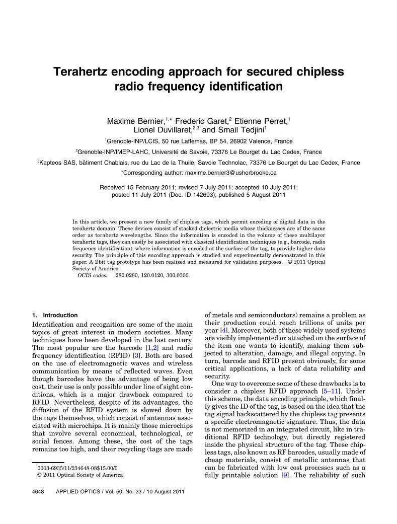
The key point of every communication system is totransmit accurate information from a transmitter toa receiver regardless of the randomly changing work-ing conditions. Therefore, it is essential to test theability of any system to work in a range of experimen-tal conditions imposed by the application itself. Inour case, the relative orientation of the tag about thetransceiver appears as a crucial parameter regard-less the technique used. Thus, in this part we areinterested in the spectral response of the terahertztag in a function of its relative disorientation aboutthe terahertz probe beam whose polarization statealso plays a major role.
Indeed, as the Fresnel reflection coefficient is afunction of the incident angle and the polarizationstate of the incoming terahertz beam [15], the spec-tral response of the tag will also depend on theseparameters. Still using the transfer matrix model,we have simulated the TE and TM terahertz fieldstransmitted through the ideal structure defined inFig. 2 for different angles of incidence θ of the tera-hertz probe beam. These numerical calculations haveshown that increasing the incident angle of the ter-ahertz beam induces spectral shifts of the TE and TMdefect modes within the considered PBG (see Fig. 5).Thus, as long as those spectral shifts can lead to theapparition or the vanishing of defect modes withinan information channel, the reliability of the THIDdevice is no more insured. Therefore, we define thenumerical acceptability of the THID tag as the criti-cal orientation value θmax, beyond which a defectmode occurs or vanishes in an information channel,involving a corruption of the stored information.Figure 6 is numerically obtained thanks to a pro-gram that automatically gets the spectral position ofthe defect mode for a given incident angle, andexhibits how the expected h01i combination encodedusing two information channels can be corrupted bythe tag disorientation θ. The defect layer thicknesshas been optimized by the previously described
routine to get the defect mode at the center of thesecond information channel when the terahertzbeam comes in with normal incident angle (θ ¼ 0°).
Considering these initial conditions and accordingto Fig. 6, for an incident angle of a TE polarized ter-ahertz beam in between 39° and 52°, the transmitted2 bit code is h00i, and becomes h10i for an angle great-er than 52°, whereas one expects h01i. The numericalacceptability of the tag for such a 2 bit code, read bya TE polarized terahertz beam, is therefore 39°.Considering a TM polarized beam, the numericalacceptability of this tag is 21°. In the general case,if we consider any elliptically polarized probe beamat the entrance of the tag, the transmitted terahertzsignal detected by the reader is the sum of the TEand TM spectral signatures. As the TE and TMdefect modes do not present the same behaviorwith the tag orientation, a degenerated defect modeoccurs with increasing θ (see Fig. 6). In this case, theterahertz reader could misinterpret the code, and thenumerical acceptability is defined as the maximumorientation beyond which the relative drift δΓ (seeFig. 7) between the TE and TMmodes is greater thanthe spectral resolution δf of the reader. One caneasily imagine that the tag immunity is specific toeach code and the initial conditions (for θ ¼ 0°), butit depends also on the bandwidth allocated to theinformation channels. As this bandwidth gets nar-rower with an increasing number of channel N, itappears that a single-defect THID tag developed toencode more information (see Fig. 4) gets moresensitive to its misalignment about the incident ter-ahertz probe beam. In turn, a compromise existsbetween orientation immunity, quantity of encodedinformation, and tag thickness when using a single-defect THID tag.
To study these behaviors, it is important to testeach orientation response of every achievable codefor a given information bit quantity. Then, the overallnumerical acceptability of the tag is fixed by thecode that presents the smallest one. Since thesecodes have been previously selected by the routinedescribed in Section 3.A, we have implemented theprogram to determinate the numerical acceptabilityjust has we did to obtain Fig. 7, for the case of a 2 bith01i code. The results are presented in Fig. 8, andFirst-order PBG
Fig. 5. (Color online) Simulated spectral response of the tag de-scribed in Fig. 2 versus its relative orientation θ about the incidentTE plane wave. For clarity reasons, the defect layer presents athickness of 390 μm to encode h01i in the first-order PBG. Verticaldashed lines delimit the information channels.
Fig. 6. (Color online) Evolution of the spectral position of the TE(solid line) and TM (dashed line) defect modes of the ideal h01i tagdescribed in Fig. 5. Horizontal lines delimit the informationchannels.
4652 APPLIED OPTICS / Vol. 50, No. 23 / 10 August 2011
have been numerically obtained for information en-coded within the first-order PBG of the single-defectTHID tag schematized in Fig. 1. The dimensions ofthe Bragg mirrors are given in caption of Fig. 2.
Regarding these last results, it appears that theTHID concept would be appropriate for securedapplications. As an example, withdrawing money ina cash machine does not require numerical accep-tance larger than 1° since the credit card is well posi-tioned in a slot, providing larger data. Therefore,an out of sight THID tag, as dimensioned above,embedded in the volume of the card would poten-tially add a 7 bit code to secure the transaction if thetag dimension is compatible with the card thickness.Some prospective solutions presented in the conclu-sion could be used to increase the storage capacity ofthe THID tags without degrading their orientationimmunity or without dramatically increasing theirthickness. But before that, it is important to validatethe encoding concept described in Section 2.B, usingthose chipless multilayer structures.
C. Experimental Validation of a 2 bit Tag
In this section, we propose to experimentally vali-date the encoding concept described in Section 2.B,using a homemade terahertz tag prototype composedof two Bragg mirrors surrounding a single-defectlayer.
The two Bragg mirrors consist of a stack of threeð75� 10Þ μm thick high resistivity 2 in: silicon wafers(layer A on Fig. 1), separated from each other by airlayers (see Fig. 1), obtained using ð300� 10Þ μmthick wedges stuck between silicon layers. The defectlayer is simply an air layer separating the two Braggmirrors. One of the two Bragg mirrors is mounted ona translation stage to get an easy and continuoustuning of the defect layer thickness ddef . After beingcalculated from Eq. (1), the tunable defect thicknesshas been roughly adjusted using the translationplate to obtain the four states encoded within thefirst-order PBG of the 2 bit tag ranging from about0.15 to 0:35THz. Then, each of the four configura-tions has been characterized in transmission by aclassical terahertz time–domain spectrometer (THz-TDS) [16] (see Fig. 9). The THz-TDS setup is nowa-days a convenient system for materials and devicescharacterized in the terahertz domain and we usedsuch a system to characterize the tags’ response andvalidate their ability to encode information.
The used THz-TDS is powered by a 600mWTi:sap-phire laser that delivers 60 fs optical pulses with acarrier wavelength of 800nm and a repetition rateof 82MHz. The laser beam is split into two beams:the first one, the pump beam, is focused on a photo-conductive emitting antenna that generates tera-hertz pulses whose spectrum spreads from 0.1 up to4THz. The second laser beam, the probe beam, illu-minates a photoconductive receiving antenna thatsamples the terahertz pulses transmitted throughthe THID tag. Both emitting and receiving antennasare made of low-temperature grown gallium arse-nide [17]. Using an optical delay line, the laser probebeam is time delayed relative to the laser pumpbeam. Thus, the receiving antenna scans the tempor-al profile of the terahertz pulse transmitted throughthe THID tag under test. A simple fast Fourier trans-form of this temporal signature leads to the spectralresponse of the tag. Finally, the transmission coeffi-cient of the tag in the frequency domain is given bythe ratio of the spectra obtained with and without asample.
Figure 10 gives the transmission coefficient of thetag for four different values of the defect layer thick-ness, leading to the four different combinations ofdefect modes in the first PBG. According to the en-coding concept previously described (see Section 2.B),the measured spectral responses (dots in Fig. 10) areinterpreted as a h00i binary sequence (curve in (a)), ah01i binary sequence (curve in (b)), a h10i binarysequence (curve in (c)), or a h11i binary sequence
Fig. 7. Simulated response of the ideal tag described in Fig. 5 andoriented with an angle θ ¼ 30° relative to the direction of propaga-tion of a circularly polarized incoming terahertz wave.
Fig. 8. (Color online) Maximum tag thickness (millimeters) andnumerical acceptability (degrees) considering a TE polarized, TMpolarized, and circularly polarized incoming terahertz wave, in afunction of the storage capacity within the first-order PBG of thesingle-defect terahertz tag described in Figs. 1 and 2. Fig. 9. (Color online) Schematic of the THz-TDS bench.
10 August 2011 / Vol. 50, No. 23 / APPLIED OPTICS 4653
(curve in (d)). The theoretical adjustments of thosespectra (solid line in Fig. 10), numerically calculatedusing the transfer matrix method [14], have givendefect thicknesses of 230, 460, 125, and 955 μm forh00i, h01i, h10i, and h11i, respectively. Extra mea-surements have also permitted precisely gettingthe thicknesses of each layer of which the two Braggmirrors are constituted, leading to a total thicknessranging from 2 to 2:6mm. These tags could poten-tially have a surface as small as the size of the foca-lized terahertz beam (≈1mm diameter). Moreover,the level contrast between defect modes and floorlevel is about 10 in magnitude (limited by the dy-namics of the THz-TDS system used), correspondingto a signal-to-noise ratio of about 20dB. Such a valuepermits a nonambiguous detection as long as thetransmission peaks stay within the right informationchannels, which is not necessarily verified, as shownin Section 3.B.
Thus, the orientation immunity of the tag proto-types has been numerically calculated using thehomemade routine described in Section 3.B to givethe results summed up in Table 1. The discrepanciesobserved between the numerical acceptances of therealized 2bit tags and the ideal cases (see Fig. 8)are explained by two main experimental reasons.First, since the defect thicknesses have been roughlyadjusted, the defect modes do not appear at thecenter of the concerned information channels (seeFig. 10). For these nonoptimized tags, the acceptablespectral shifts induced by the tags’ disorientation aregetting smaller than for the ideal cases: the realizedtags present worse numerical acceptances than theone predicted (see Fig. 8). Concerning the storagecapacity of the realized THID tags, since the THz-TDS used to measure the temporal signatures ofeach tag presents a spectral resolution of 3GHz,
the approximate number of available encoding chan-nels is 60. In turn, according to Eq. (7), the potentialstorage capacity within the first-order PBG of therealized THID tags is about 7 bits. Thus, while exper-imental validation could have been done for largerencoded information, it would be a waste of timesince it would have confirmed what we obtain withthis simple four state example.
4. Conclusion
In this article, we have experimentally validated anew concept of encoding information in the terahertzdomain. The whole dielectric chipless tags intro-duced present no metallic parts and are made of asimple stack of silicon and air layers, dimensionedto code secured 2 bit data in a spectral range spread-ing from 0.15 to 0:35THz. Note that handy commer-cial solutions are available in this spectral range [18]to replace the sophisticated THz-TDS as a THIDreader. These structures can be potentially used tostore up to 10 bits by taking advantage of higherorder PBGs. The realized tags have thicknesses inthe millimeter range and a surface of the order of1mm2. It presents an orientation immunity of 20°,16°, and 13°, considering a TE, TM, or circularlypolarized incoming terahertz probe beam. Optimiza-tion of the dimensions of the layers could almost dou-ble these values.
The number of information channels imposed bythe spectral resolution of the terahertz reader andthe Bragg mirrors’ transmission responses limits theperformances of the whole recognition system. Eventhough this number can be increased by improvingthe spectral resolution δf of the reader and/or bybroadening the PBG bandwidth Δf (using, for exam-ple, Bragg mirrors made of metamaterials [19]), thisarticle has shown that a terahertz tag based on asingle-defect layer presents a compromise betweenits storage capacity and its orientation immunity,which is of major importance for any practical devel-opment. But solutions that are constituted of severalindependent defect layers could permit an increase ofthe storage capacity without degrading the orienta-tion immunity of the terahertz tag or without drama-tically increasing its thickness.
Therefore, chipless terahertz tags constitute a veryattractive solution devoted to specific or everyday lifeidentification applications. Indeed, getting rid of thechip permits development of low-cost green tags, asthe multilayer structure, which contains the usefulinformation, could be made of recyclable materialslike polymers. Developing such “solid” THID tags
(a)
(c) (d)
(b)
Fig. 10. (Color online) Measured (dots) and simulated (solid line)transmission coefficient of the realized multilayer structureproviding (a) h00i code (ddef ¼ 230 μm), (b) h01i code (ddef ¼460 μm), (c) h10i code (ddef ¼ 125 μm), and (d) h11i code (ddef ¼955 μm) within the usable bandwidth of the first-order PBGdelimited by the vertical dashed line.
Table 1. Numerical Acceptability of the Realized 2 bit Terahertz Tags
DefaultThickness (μm)
BinaryCode
TE ProbeBeam
TM ProbeBeam
Circularly PolarizedProbe Beam
230 h00i 38° 16° 16°460 h01i 20° 21° 19°125 h10i >60° 33° 13°955 h11i 27° 29° 21°
4654 APPLIED OPTICS / Vol. 50, No. 23 / 10 August 2011

would lead to a better mechanical robustness in com-parison to the presented Si–air prototypes where theair layers’ thicknesses are sensitive to transport con-ditions. Moreover, their passive character, small size,potentially high storage capacity, and encoding involume make them hardly forgeable, which is idealfor secured recognition applications.
And last but not least, since the proposed terahertzsolution encodes information in volume, it is compa-tible with the existing and widely spread RFID tech-nique, where information is encoded at the surfaceof the tag. Thus, one can imagine a hybrid solutionmade of an RFID antenna printed on a THID tag tosecurely encode a large amount information.
The authors would like to thank Grenoble-INP forsupporting this project via the Bonus Qualité Re-cherche (BQR) programme.
References1. N. J. Woodland and B. Silver, “Classifying apparatus and
method,” U.S. patent 2,612,994 (7 October 1952).2. K. Finkenzeller,RFIDHandbook: Fundamentals and Applica-
tions (Wiley, 2004).3. H. Stockman, “Communication by means of reflected power,”
Proc. IRE 36, 1196–1204 (1948).4. R. Das and P. Harrop, “Printed and chipless RFID forecasts,
technologies & players 2009–2019” (IDTechEx, 2010).5. S. Tedjini, E. Perret, V. Deepu, and M. Bernier, “Chipless tags,
the RFID next frontier,” presented at the 20th TyrrhenianWorkshop on Digital Communications, Sardinia, Italy, Sep-tember 2009.
6. C. S. Hartmann, “A global SAW ID tag with large datacapacity,” Proc. IEEE Ultrason. Symp. 1, 65–69 (2002).
7. L. Zheng, S. Rodriguez, L. Zhang, B. Shao, and L. R. Zheng,“Design and implementation of a fully reconfigurable chiplessRFID tag using inkjet printing technology,” in IEEE Interna-tional Symposium on Circuits and Systems (IEEE, 2008), pp.1524–1527.
8. C. Mandel, M. Schüssler, M. Maasch, and R. Jakoby,“A novel passive phase modulator based on LH delay linesfor chipless microwave RFID applications,” in Interna-tional Microwave Workshop on Wireless Sensing (IEEE,2009), pp. 1–4.
9. S. Preradovic and N. C. Karmakar, “Design of fully printableplanar chipless RFID transponder with 35bit data capacity,”in Proceedings of the 39th European Microwave Conference(EuMC, 2009), pp. 13–16.
10. I. Jalaly, “RF barcodes using multiple frequency bands,” in2005 IEEE MTT-S International Microwave Symposium Di-gest (IEEE, 2005), pp. 1 –4.
11. I. Baldin and N. C. Karmakar, “Phase-encoded chipless RFIDtransponder for large-scale low-cost applications,” IEEEMicrow. Wireless Compon. Lett. 19, 509–511 (2009).
12. T. Numai, Fundamentals of Semiconductor Lasers (Springer,2004), Chap. 4.2.
13. T. Numai, Fundamentals of Semiconductor Lasers (Springer,2004), Chap. 4.3.
14. H. Nemec, L. Duvillaret, F. Quemeneur, and P. Kužnel, “Defectmodes caused by twinning in one dimensional photoniccrystal,” J. Opt. Soc. Am. B 21, 548–553 (2004).
15. M. Born and E. Wolf, Principles of Optics: ElectromagneticTheory of Propagation, Interference and Diffraction of Light,”7th ed. (Cambridge University, 1999), Chap. 1.6.
16. M. van Exter and D. Grischkowsky, “Characterization of anoptoelectronic terahertz beam system,” IEEE Trans.Microwave Theory Tech. 38, 1684–1691 (1990).
17. L. Duvillaret, F. Garet, J. F. Roux, and J. L. Coutaz, “Analyticalmodeling and optimization of terahertz spectroscopy experi-ment using photoswitches as antennas,” IEEE J. Sel. Top.Quantum Electron. 7, 615–623 (2001).
18. H. Quast and T. Loeffer, “3D terahertz tomography for mate-rial inspection and security,” in 34th International Conferenceon Infrared, Millimeter, and Terahertz Waves (IRMMW, 2009),pp. 1–2.
19. X. M. Shen, X. F. Chen, M. P. Jiang, and D. F. Shi, “Transmis-sion spectra of one dimensional photonic crystal includingnegative refractive index media,” Optoelectron. Lett. 1,201–204 (2005).
10 August 2011 / Vol. 50, No. 23 / APPLIED OPTICS 4655