tem study of the sol-gel oxide thin films - formatex · tem study of the sol-gel oxide thin films...
TRANSCRIPT

TEM study of the sol-gel oxide thin films
V.S. Teodorescu1 and M-G. Blanchin2
1 National Institute of Material Physics, 105 bis Atomistilor, 077125 Bucharest-Măgurele, Romania
2 Université de Lyon, Univ. Lyon I, ILM, CNRS-UMR 5306,69622 VILLEURBANNE, CEDEX, France
This paper presents a comparative transmission electron microscopy (TEM) study of structure and morphology of different sol-gel oxide films, showing relevant structural features resulting from film deposition and subsequent annealing. We expose several details of the TEM specimen preparation, cross section and plan view and discuss the main features which can be observed using these specimens. Results on the various sol-gel film oxides, tin oxide, indium oxide, zinc oxide, hafnium oxide and others, are presented and compared, following different types of annealing used for film crystallization: furnace annealing, rapid thermal annealing and pulsed laser annealing.
Keywords: oxide sol-gel films; XTEM; electron irradiation; pulsed laser annealing
1. Introduction
The sol-gel oxide thin films are nowadays present in a large number of applications: protective coatings, surface opto-mechanical modifications, transparent oxide conductor contacts and others. The sol-gel films are obtained from various precursors, inorganic or metal-organic, using mainly two deposition methods: dipping and spinning [1]. After their deposition, the sol-gel films are amorphous and soft and contain an important quantity of solvent and precursor species. After drying the solvent traces are removed. The subsequent thermal treatment induces the densification of the amorphous structure and removes also the remaining precursor traces. At this stage, the sol-gel films have a dense amorphous structure with a high density of nanopores. The last annealing step takes place at higher temperature and induces crystallization and the final film nanostructure formation. The microscopic structure of the sol-gel films can be studied in detail by transmission electron microscopy (TEM), from the amorphous structure state, to the final crystalline one. The plan view, cross section (XTEM), or other special methods for TEM specimen preparation, allows the complete characterization of the structure and the morphology of the sol-gel films in different annealing stages. Some structural studies of the sol-gel films are made using scanning electron microscopy (SEM) or atomic force microscopy (AFM). These two methods are fast, but show only the surface topography of the film, which is not always directly related with the inside film structure. The TEM study is more complicated, involves more time for specimen preparation and observations, but is the only way to study the film volume structure and morphology. The crystallization process of the sol-gel films is not similar for all oxides. There are significant differences in the final morphology and structure of different type of oxide films. Some of the amorphous structures are sensitive to the electron beam irradiation, which induces in-situ nanocrystallization. In the same time, the duration and the annealing method are very important for the final film morphology. The classical thermal (furnace) annealing (CTA), the rapid thermal annealing (RTA) and the pulsed laser annealing (PLA), are herein exemplified. The morphology and the structure of a thick multilayer sol-gel film, obtained by multiple depositions are different for each deposited layer due to the different number of annealing time supported by the successive deposited layers. Depending on the annealing method and atmosphere, the film develops inside porosity, surface crust and also some stress field, which appears in the oxide lattice or at the interface between the deposited layers. This stress field is partially released by extended defects generation, which can appear either in the film or in the substrate. In the present paper we expose several details of the specimen preparation and results for the several sol-gel films oxides, such as: ATO(SnO2:Sb), ITO(In2O3:Sn), TiO2, HfO2 , ZnO and BTO (BaTiO3). We show comparatively some characteristic structural features of different sol-gel oxide films, revealed by the TEM study, and deal with the potential problems, which may appear.
2. TEM specimen preparation
TEM specimens from the sol-gel thin films deposited on glass or silicon wafers can be prepared in several ways. The most effective method is the cross section (XTEM) preparation. This technique consists in mechanical cutting of small rectangular pieces, gluing these pieces face to face with special epoxy, cutting slices with thickness of about 0.5 mm followed by mechanical polishing with different diamond powder grade to the limit of less than one micron and finally by ion milling. This process is schematically shown in Fig. 1.
Microscopy: advances in scientific research and education (A. Méndez-Vilas, Ed.)__________________________________________________________________
© FORMATEX 2014 903

In some cases, the plan view observations are necessary. In this preparation, the mechanical polishing and the ion thinning are performed only from the substrate side of the sample (see Fig.2). Function of the film thickness, the film only or the film superposed on its substrate can be observed. One of the problems of the plan view preparation from the crystallized film is the stress field developed in the film structure [2]. This stress field induces high tensions inside the film and at the film-substrate interface. This stress field relaxes when the plan view specimen is enough thin during the ion milling and the specimen can be broken and lost.
Fig. 2 Schematics of the plan view specimen preparation. Specimen section before the ion milling (a) and after the ion milling (b)
One alternative to the plan view preparation is the mechanical extraction of small fragments from the film and its substrate using a thin diamond tip [3], and deposit these fragments on a carbon copper grid. Some fragments are very thin and the obtained TEM images can show even high resolution details. This method is fast and can give information even for the film thickness if the electron microscope has a high angle goniometer. Fig.3 illustrates the type of images which are commonly observed using the XTEM specimens. The images are performed on a XTEM specimen prepared from an amorphous dried BiTiO3 (BTO) sol-gel film. The selected area electron diffraction (SAED) pattern in Fig. 3d shows the diffuse ring of the amorphous film structure (arrowed) superposed with the diffraction spots of the [110] zone axis of the Si substrate. In the case of films deposited on Si [100] wafers, the XTEM specimen must be oriented in the microscope (using the goniometer stage) to align the electron beam direction parallel with the film surface. In this way, the film interface with the substrate can be observed at high resolution (see Fig. 3c) and the film thickness determination is very accurate.
3. Structure of sol-gel oxide films
3.1 ATO and ITO sol-gel films
Transparent Conducting Oxides (TCO) like ITO (In2O3: Sn) and ATO (SnO2: Sb) films can be successfully deposited on different substrates by the sol-gel method [4-11]. Data about the morphology and the structural modifications of TCO films during their drying, densification and crystallization stages were revealed by XTEM [4,9]. After deposition and drying, these films are amorphous and non-conductive. Conductivity is obtained after their crystallization. This structural transformation is a key factor for some applications and the electron microscopy observations are very effective for the study of the crystallization process. After drying of an ATO sol-gel film at a temperature of 150oC, crystalline nuclei of about 2 nm are formed embedded in the amorphous matrix, but the film remains insulator. After the classical (CTA) thermal annealing at 500oC, the film structure crystallizes and become conductor. Fig. 4 shows the structural differences between the two cases. The crystallized film has grain size in the range of 5 to10 nm, as visible in Fig. 4b. The film conductivity grows with the size of the crystalline grains [4].
Fig. 1 Schematics of the cross section (XTEM) specimen preparation (a) and the section of the final thinned specimen (b)
Microscopy: advances in scientific research and education (A. Méndez-Vilas, Ed.)__________________________________________________________________
© FORMATEX 2014904

During the crystallization process, a dense “crust” is formed at the film surface due to the very active surface diffusion during crystallization. The XTEM images reveal very well the successive layers in the section of multilayered films due to this crust formation for each sol-gel deposited layer [4, 5]. The rapid thermal annealing (RTA) of the ATO films leads to similar morphology as the case of classical annealing, but the structure is more uniform and the grain size smaller. The crusts between the deposited layers remain visible but have a smaller thickness compared with the CTA case, as shows in Fig. 5a.
The crust formation and evolution insight the volume of the multilayer film is exposed schematically in Fig 6. The subsequent annealing performed after each new deposited layer, induces the densification of the embedded layers by reducing the nanopore size. Because in the crust region the structure is already dense, a stress field develops at the level of the embedded crusts, which partially relaxes by lattice defects formation in the crystallite grains. Some micro-twinning defects can be observed inside the crystallites forming the crusts in multilayered films [4]. This indicates the high level of stress reached in some ATO crystallites forming the internal crusts, during subsequent densification induced by the successive annealing. This “crust” model can be applied to the sol-gel oxide films which have crystalline grain size smaller than the thickness of the deposited layer.
Fig. 3 The main type of image areas which can be observed on a XTEM (BTO) specimen:
(a) low magnification image, (b) medium magnification image, (c) high resolution image, (d) SAED pattern of the film and the Si substrate in [110] orientation.
The BTO film was annealed for 10 minutes at 400oC. The film structure is amorphous and is stable under the electron beam irradiation during the HRTEM observations.
Fig. 4 High resolution (HRTEM) details of the XTEM specimen prepared from an ATO sol-gel film after drying at 150oC for 45 minutes (a) and after furnace annealing at 500oC for 45 minutes (b). The dried amorphous film is insulator and the film annealed at 500oC is crystallized and conductor.
Microscopy: advances in scientific research and education (A. Méndez-Vilas, Ed.)__________________________________________________________________
© FORMATEX 2014 905

Fig. 5 Low magnification XTEM images of the multilayer (5 layers) ATO sol-gel film (a) and ITO sol-gel film (b). Fig. 4a shows the comparison between the same ATO film sample annealed by RTA and CTA. (S – is the pyrex substrate , and 1 to 5 are the subsequent deposited layers). Fig. 5b shows a ITO film which has the crystallite size bigger than the similar ATO film. ITO film presents also quite big nanopores with size which decreases from the top layer to the bottom layer (arrowed a- in the top layer, b- in the middle and c at the bottom).
Fig. 6 Schematics of the cross section of a multilayer sol-gel film morphology. The crust appears by annealing on the t0p of every deposited layer and remains and develops embedded in the film volume during the subsequent annealing.
Classical thermal annealing holds only for thermal resistant substrates. In the case of polymer substrates for instance, heating must be confined in the film volume. This can be obtained using excimer laser radiation in ultraviolet. If the laser photon energy is higher than the band gap energy of the oxide, the laser radiation will be absorbed in a thickness of about 1/α, where α is the absorption coefficient of laser radiation. This laser absorption depth in the ATO dried sol-gel films is of the order of 20 nm in the case of ArF excimer radiation (λ =193 nm). Sol-gel film annealing using excimer lasers allows the crystallization depth control in the film thickness [12-14]. Fig. 7 shows a XTEM image of an ATO sol-gel film after laser annealing. Only the top part (about 100 nm) of the film is crystallized. Laser processing allows heating of the oxide film surface at high temperatures. However, temperatures larger than the melting point of the oxides are not useful for crystallization because the film surface becomes less smooth and the ablation process can induced.
Microscopy: advances in scientific research and education (A. Méndez-Vilas, Ed.)__________________________________________________________________
© FORMATEX 2014906

3.2 TiO2 sol-gel film
In Fig. 8 is shown a medium magnification XTEM image of a 500 nm thick anatase sol-gel film formed by 5 deposited layers. The crusts formed after each annealing process are visible, like in the case of the ATO sol-gel films. The morphology and the porosity of the TiO2 sol-gel film can be better observed in the plan view specimen prepared from a monolayer deposited film as shown in Fig.9. Due to their photocatalytic properties, the doped TiO2 film and powders obtained by sol-gel method are intensively studied [15].
Fig. 9 TEM images obtained on a plan view specimen prepared from a monolayer TiO2 anatase sol-gel film deposited on glass substrate after annealing at 500oC for 30 minutes. a - low magnification image; b - high resolution image and c- corresponding SAED pattern showing the presence of the anatase phase.
Fig. 7 ATO sol-gel film annealed with 10 laser pulses of excimer laser (ArF, 193 nm) with the fluence of 36 mJ/cm2. From the XTEM image we can consider the top part of the film (T) a region in which the melting takes place. Structure of this region is not dependent on the number of laser pulses. This shows that the laser melting depth is quite the same at every applied laser pulse. The thickness of the T region is of the same order of magnitude as the laser radiation absorption length. The medium part of the film (M) is crystallized by the heat diffusion from the top part and can be considered as a thermal affected region. Finally, the region at the film base (B) near the pyrex substrate is amorphous and not affected by the laser irradiation. The whole film thickness will crystallize when increasing the laser pulse number. In this way, the crystallization depth of the film can be controlled by the laser pulses number and the laser fluence [12-14]
Fig. 8 XTEM image of a multilayer TiO2 anatase sol-gel film obtained by 5 layers deposition and CTA annealing at 500oC.
Microscopy: advances in scientific research and education (A. Méndez-Vilas, Ed.)__________________________________________________________________
© FORMATEX 2014 907

3.3 HfO2 sol-gel film and electron beam sensitivity
The HfO2 sol-gel films have been produced on the base of ethoxide, pentadionate and chloride precursors [16 ]. If the annealing temperature is less than 500oC, the film remains amorphous. The resulted HfO2 sol-gel film is very thin, with thickness of about 10 to 15 nm for each layer deposition. Multilayer film can be obtained by subsequent layer deposition after each annealing for amorphous phase densification or after deposited layer crystallization. The crust formation is less visible in this case because the crystallization process is fast, producing large grains with inside nanopores. This feature shows that the crystallization process starts from few nuclei in the amorphous phase. The crystallization front moving fast goes around the existing pores, resulting in a quasi-coherent crystalline lattice with inside nanopores, as can be observed in Fig. 10 and Fig.11.
Fig. 11 Plan view image (a) and the corresponding SAED pattern (b) of the HfO2 sol-gel film obtained from pentadionate precursor after annealing at 600oC. The plan view image reveals a large HfO2 crystalline grain in [111] orientation, which contains a high density of inside nanopores. The SAED pattern (b) shows diffraction spots from the HfO2 film and the silicon substrate in [001] orientation. The HfO2 crystallized grain contains a lot of defects related to the nanopores presence. This large crystalline grain in fact a mosaic of little disoriented nanocrystalline domains, as the angular dispersion of the (220) HfO2 diffraction spots shows. The presence of nanopores is more visible in the plan view image.
The amorphous HfO2 sol-gel films are very sensitive to the electron beam irradiation. The amorphous phase crystallizes under the electron beam irradiation producing a high density of nucleation sites and finally nanometric size crystallites, as shown in Fig.12. This effect is a non thermal one. The temperature rise on the specimen is low even for high density of electron current [16], if the specimen is well prepared. We expect a radiolysis character of this transformation because it happens also in time at lower electron density or lower electron beam energy. This sensitivity to the electron beam irradiation is normal for ionic materials and was not observed on sol-gel amorphous oxide as ATO, ITO or ZnO.
Fig. 12 HRTEM observation of a HfO2 sol-gel film deposited on silicon substrate: (a) film structure after the first 10s of high resolution observations (b) the same structure after 120 s of observations under a electron density of 10 A/cm2
Fig. 10 XTEM image of a monolayer HfO2 sol-gel film obtained from pentadionate precursor [16,17], after crystallization by CTA annealing at 600oC for 30 minutes. The film has a thickness of about 12 nm. The size of the crystalline grains is much larger than the film thickness. The SiO2 layer at the interface with the Si substrate is characteristic feature for the case of the HfO2 films deposited on silicon wafers.
Microscopy: advances in scientific research and education (A. Méndez-Vilas, Ed.)__________________________________________________________________
© FORMATEX 2014908
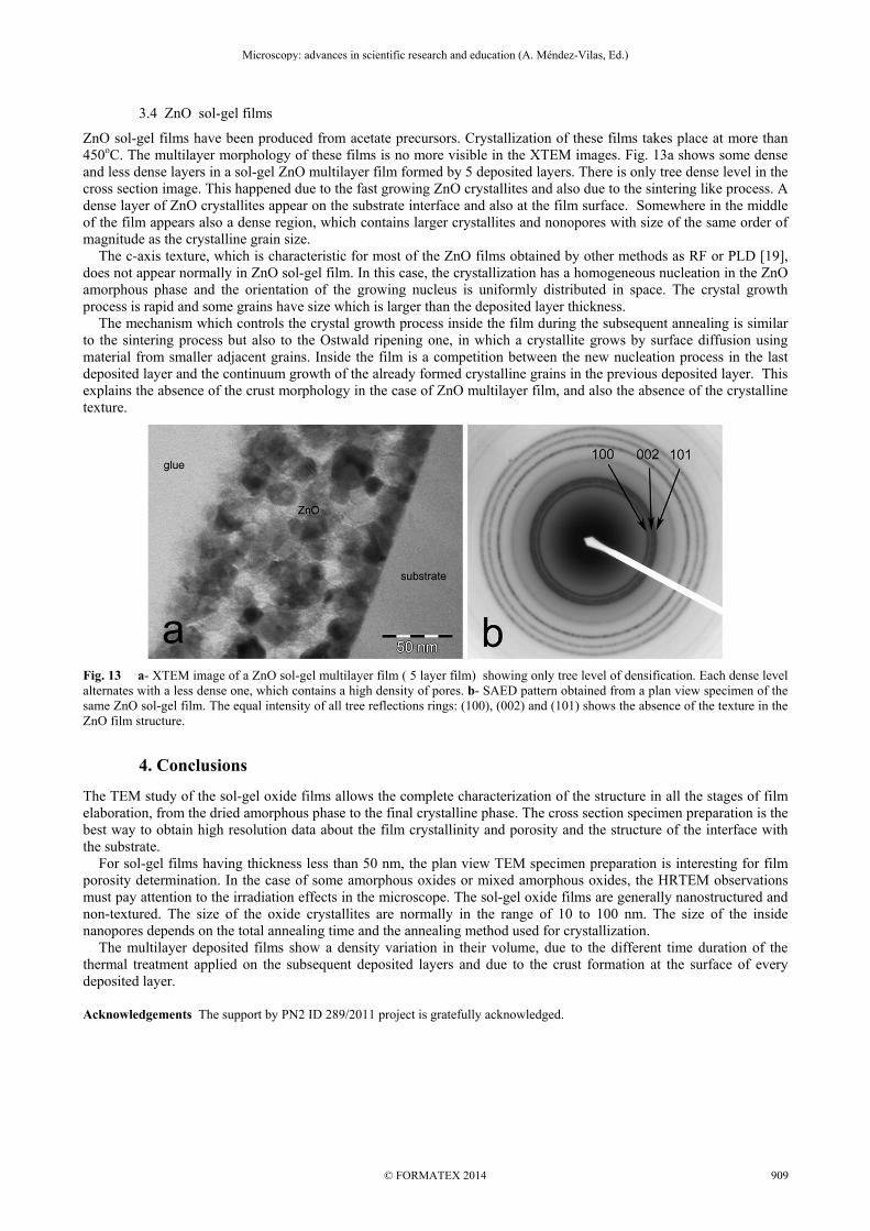
3.4 ZnO sol-gel films
ZnO sol-gel films have been produced from acetate precursors. Crystallization of these films takes place at more than 450oC. The multilayer morphology of these films is no more visible in the XTEM images. Fig. 13a shows some dense and less dense layers in a sol-gel ZnO multilayer film formed by 5 deposited layers. There is only tree dense level in the cross section image. This happened due to the fast growing ZnO crystallites and also due to the sintering like process. A dense layer of ZnO crystallites appear on the substrate interface and also at the film surface. Somewhere in the middle of the film appears also a dense region, which contains larger crystallites and nonopores with size of the same order of magnitude as the crystalline grain size. The c-axis texture, which is characteristic for most of the ZnO films obtained by other methods as RF or PLD [19], does not appear normally in ZnO sol-gel film. In this case, the crystallization has a homogeneous nucleation in the ZnO amorphous phase and the orientation of the growing nucleus is uniformly distributed in space. The crystal growth process is rapid and some grains have size which is larger than the deposited layer thickness. The mechanism which controls the crystal growth process inside the film during the subsequent annealing is similar to the sintering process but also to the Ostwald ripening one, in which a crystallite grows by surface diffusion using material from smaller adjacent grains. Inside the film is a competition between the new nucleation process in the last deposited layer and the continuum growth of the already formed crystalline grains in the previous deposited layer. This explains the absence of the crust morphology in the case of ZnO multilayer film, and also the absence of the crystalline texture.
Fig. 13 a- XTEM image of a ZnO sol-gel multilayer film ( 5 layer film) showing only tree level of densification. Each dense level alternates with a less dense one, which contains a high density of pores. b- SAED pattern obtained from a plan view specimen of the same ZnO sol-gel film. The equal intensity of all tree reflections rings: (100), (002) and (101) shows the absence of the texture in the ZnO film structure.
4. Conclusions
The TEM study of the sol-gel oxide films allows the complete characterization of the structure in all the stages of film elaboration, from the dried amorphous phase to the final crystalline phase. The cross section specimen preparation is the best way to obtain high resolution data about the film crystallinity and porosity and the structure of the interface with the substrate. For sol-gel films having thickness less than 50 nm, the plan view TEM specimen preparation is interesting for film porosity determination. In the case of some amorphous oxides or mixed amorphous oxides, the HRTEM observations must pay attention to the irradiation effects in the microscope. The sol-gel oxide films are generally nanostructured and non-textured. The size of the oxide crystallites are normally in the range of 10 to 100 nm. The size of the inside nanopores depends on the total annealing time and the annealing method used for crystallization. The multilayer deposited films show a density variation in their volume, due to the different time duration of the thermal treatment applied on the subsequent deposited layers and due to the crust formation at the surface of every deposited layer.
Acknowledgements The support by PN2 ID 289/2011 project is gratefully acknowledged.
Microscopy: advances in scientific research and education (A. Méndez-Vilas, Ed.)__________________________________________________________________
© FORMATEX 2014 909

References
[1] Brinker CJ and Scherer GW, Sol-Gel Science: The physics and Chemistry of sol-Gel Processing, Academic Press 1990 [2] Brenier R, Urlacher C, Mugnier J, Brunel M, Stress development in amorphous zirconium oxide films prepared by sol-gel
Processing, Thin Solid Films, 1999;338:136-141. [3] Teodorescu VS, Blanchin MG, Fast and simple specimen preparation for TEM studies of oxide films deposited on silicon
wafers, Microscopy and Microanalysis, 2009; 15(1): 15-19. [4] Sandu CS, PhD these, , DPM-University Claude Bernard Lyon 1, Densification of transparent conducting oxide SnO2 :Sb
films elaborated by SoL-Gel route : a comparative study of different annealing processes. Lyon 2003 [5] Sandu CS, Roger JA, Canut B, Blanchin MG, Teodorescu VS, Densification and carier concentration in Sb doped sol-gel
obtained oxide , Radiation Effects and Defects in Solids. 2001; 156: 129-34. [6] Daoudi K, Canut B, Blanchin MG, Sandu CS, Teodorescu VS, Roger JA, Tin doped indium oxide thin films deposited by sol-
gel dip coating technique, Material Science and Engineering. 2002; C21(1-2): 313-17. [7] Daoudi K, Sandu CS, Teodorescu VS, Ghica C, Canut B, Blanchin MG, Roger JA, Oueslati M, Bessais , Rapid thermal
annealing procedure for densification of sol-gel indium in oxide thin films, Crystal Engineering, 2002; (3-4) Sp. Iss.: 187-93 [8] Boudiar T, Sandu CS, Canut B, Blanchin MG, Teodorescu VS, Roger JA, Interest of Rapid Thermal Annealing (RTA) for the
elaboration of SnO2:Sb Transparent Conducting Oxide by the Sol-Gel technique, Journal of Sol-Gel Science and Technology.2003; 26: 1067-70.
[9] Stoica TF, Teodorescu VS, Blanchin MG, Stoica TA, Gartner M, Losurdo M, Zaharescu M , Morphology, structure and optical properties of sol-gel ITO thin films, Materials Science and Engineering B. 2003;101:222-26.
[10] Daoudi K, Canut B, Blanchin MG, Sandu CS, Teodorescu VS, Roger JA, Densification of In2O3:Sn multilayered films elaborated by dip-coating sol-gel route, Thin Solid Films. 2003;445(1): 20-25.
[11] Stoica TF, Gartner M, Stoica T, Losurdo M, Teodorescu VS, Blanchin MG, Zaharescu M, Properties of high porosity sol-gel derived indium-tin oxide films, Journal of Optoelectronics and Advanced Materials. 2005;7: 2353-58.
[12] Sandu CS, Teodorescu VS, Ghica C, Canut B, Blanchin MG, Roger JA, Brioude A, Bret T, Hoffmann P, Garapon C, Densification and crystallization of SnO2:Sb sol-gel films using excimer laser annealing, Applied Surface Science. 2003;208: 382-87.
[13] Sandu CS, Teodorescu VS, Ghica C, Hoffmann P, Bret T, Brioude A, Blanchin MG, Roger JA, Canut B, Croitoru M, Excimer laser crysallization of SnO2:Sb sol-gel films, Journal of Sol-Gel Science and Technology, 2003; 28: 227-34.
[14] Teodorescu VS, Ghica C, Sandu CS, Maraloiu AV, Blanchin MG, Canut B, Roger JA, Nanoscale crystallization process in ATO sol-gel films using excimer laser annealing, Digest Journal of Nanomaterials and Biostructures. 2006;1: 61-69.
[15] Yu J, Zhao X, Zhao Q, Photocatalytic activity of nanometer TiO2 thin films prepared by the sol-gel method, Materials Chemistry and Physics. 2001; 1-3: 25-29.
[16] Blanchin MG, Canut B, Lambert Y, Teodorescu VS, Barău A, Zaharescu M, Structure and dielectric properties of HfO2 films prepared by sol-gel method, Journal of Sol-Gel Science and Technology. 2008;47(2): 165-72.
[17] Zaharescu M, Teodorescu VS, Gartner M, Blanchin MG, Barau A, Anastasescu M , Correlation between the method of preparation and the properties of the sol-gel HfO2 thin films, Journal of Non-Crystalline Solids. 2008;354 (2-9): 409-15.
[18] Williams Db and Carter CB, Transmission Electron Microscopy, Plenum Press 1996 [19] Niculescu M, Anastasescu M, Preda S, Calderon-Moreno JM, Osiceanu P, Teodorescu VS, Maraloiu AV, Kampylafka V,
Aperathitis E, Modreanu M, Investigation of microstructural properties of nitrogen doped ZnO thin films formed by magnetron sputtering on silicon substrate , Journal of Optoelectronics and Advanced Materials. 2010;12(5) :1045-1051.
Microscopy: advances in scientific research and education (A. Méndez-Vilas, Ed.)__________________________________________________________________
© FORMATEX 2014910