teledyne imaging sensors: infrared imaging technologies ... · teledyne imaging sensors: infrared...
TRANSCRIPT

Copyright 2008 Society of Photo-Optical Instrumentation Engineers This paper was published in the Proceedings of the SPIE Conference on Astronomical Instrumentation (2008, Marseille, France) and is made available as an electronic reprint with permission of SPIE. One print or electronic copy may be made for personal use only. Systematic or multiple reproduction, distribution to multiple locations via electronic or other means, duplication of any material in this paper for a fee or for commercial purposes, or modification of the content of the paper are prohibited.
page 1 of 14
Teledyne Imaging Sensors: Infrared imaging technologies for Astronomy & Civil Space
James W. Beletic*, Richard Blank*, David Gulbransen, Donald Lee, Markus Loose,
Eric C. Piquette, Thomas Sprafke, William E. Tennant, Majid Zandian, and Joseph Zino
Teledyne Imaging Sensors Camarillo, California, USA 93012
ABSTRACT
Teledyne Imaging Sensors develops and produces high performance infrared sensors, electronics and packaging for astronomy and civil space. These IR sensors are hybrid CMOS arrays, with HgCdTe used for light detection and a silicon integrated circuit for signal readout. Teledyne manufactures IR sensors in a variety of sizes and formats. Currently, the most advanced sensors are based on the Hawaii-2RG (H2RG), 2K×2K array with 18 µm pixel pitch. The HgCdTe detector achieves very low dark current (<0.01 e-/pixel/sec) and high quantum efficiency (80-90%) over a wide bandpass. Substrate-removed HgCdTe can simultaneously detect visible and infrared light, enabling spectrographs to use a single focal plane array (FPA) for Visible-IR sensitivity. The SIDECARTM ASIC provides focal plane electronics on a chip, operating in cryogenic environments with very low power (<11 mW). The H2RG and SIDECAR have been qualified to NASA Technology Readiness Level 6 (TRL-6). Teledyne continues to advance the state-of-the-art and is producing a high speed, low noise array designed for IR wavefront sensing. Teledyne is also developing a 4K×4K, 15 µm pixel infrared array that will be a cost effective module for the large focal planes of the Extremely Large Telescopes and future generation space astronomy missions.
Keywords: IR, Imaging, ROIC, FPA, electronics, packaging, H2RG, Speedster128, H4RG, SIDECAR ASIC, Teledyne
1. DEVELOPMENTS SINCE SPIE 2006 1.1 Transition from Rockwell Scientific Company to Teledyne Imaging Sensors Since the 2006 SPIE Astronomical Instrumentation meeting, much has taken place in Camarillo, California, the home of Teledyne Imaging Sensors (TIS). In September 2006, Teledyne Technologies acquired Rockwell Scientific Company, and incorporated Teledyne Scientific & Imaging (TS&I) as a strategic business unit. Within TS&I, Teledyne Imaging Sensors provides focus on imaging sensors, and a market segment entitled “Astronomy & Civil Space” was established to serve the Astronomy and Earth observation communities. To strengthen the capabilities and breadth of IR product offerings, Teledyne acquired Judson Technologies in February 2008. Teledyne Judson Technologies provides IR image sensor technologies for laboratory applications, OEM systems, defense applications, and space missions. Teledyne Technologies is a high technology company that has been successful by focusing on customer satisfaction and continually improving operational processes to efficiently produce high performance products. This environment has already strengthened Teledyne Imaging Sensors and is beneficial to the astronomical community since it enables TIS to continue to provide state-of-the-art imaging arrays to the scientific community in the most cost effective way.
1.2 Major deliveries and developments in past 2 years During the past two years, Teledyne Imaging Sensors has delivered high performance infrared sensors to several major astronomical facilities and space missions. The mission / instrument, array sizes, number of science grade devices that are integrated into the instrument (N), and cutoff wavelength (λco), are as follows:
WISE – Wide-field Infrared Survey Explorer (imager) − 1024×1024 pixel arrays (N = 2), HgCdTe (λco = 4.2 µm, 5.2 µm)
Moon Mineralogy Mapper (spectrograph) − 640×480 pixel array (N = 1), HgCdTe (substrate-removed, λ = 0.4-3.0 µm)
*Correspondence: [email protected], [email protected]

Copyright 2008 Society of Photo-Optical Instrumentation Engineers This paper was published in the Proceedings of the SPIE Conference on Astronomical Instrumentation (2008, Marseille, France) and is made available as an electronic reprint with permission of SPIE. One print or electronic copy may be made for personal use only. Systematic or multiple reproduction, distribution to multiple locations via electronic or other means, duplication of any material in this paper for a fee or for commercial purposes, or modification of the content of the paper are prohibited.
page 2 of 14
OCO – Orbiting Carbon Observatory (spectrographs) − 1024×1024 pixel arrays (N = 3), HgCdTe (λco = 2.5 µm), Visible silicon PIN (λ = 0.4-1.1 µm)
Hubble Space Telescope (HST), Wide Field Camera 3 – WFC3 (imager) − 1024×1024 pixel array (N = 1), HgCdTe (substrate-removed, λ = 0.6-1.7 µm)
James Webb Space Telescope (JWST), Near Infrared Spectrograph (NIRSpec), Near Infrared Camera (NIRCam) and Fine Guidance Sensor (FGS) (imagers and spectrograph)
− 2048×2048 pixel arrays (N = 15), HgCdTe (substrate-removed, λ = 0.6-2.5 µm and 0.6-5.0 µm) − Engineering model deliveries have been made, with flight units to be completed during 2008
Carnegie Observatory, Four Star (imager) − 2048×2048 pixel arrays (N = 4), HgCdTe (substrate-removed, λ = 0.6-2.5 µm)
European Southern Observatory, X-Shooter (spectrograph) − 2048×2048 pixel arrays (N = 1), HgCdTe (substrate-removed, λ = 0.6-2.5 µm)
Additionally, during the past 2 years, TIS has made several significant technological advancements1,2, including:
Substrate-removal of HgCdTe became a routine process for IR arrays. Substrate-removed HgCdTe (see section 3) increases quantum efficiency (QE) in the near IR, provides visible response, eliminates fringing in the substrate, and removes fluorescence from cosmic rays that are absorbed in the substrate.
The H2RG image array and the SIDECAR ASIC reached TRL-6 and are fully qualified for use in space astronomy instrumentation.
The SIDECAR ASIC was selected for the repair of the Advanced Camera for Surveys (ACS) instrument of the Hubble Space Telescope. Installation will be made during the October 2008 servicing mission.
Spaceflight packages were developed for the SIDECAR ASIC: JWST cryogenic package, and HST hermetically sealed package.
The first SIDECAR ASICs were delivered to ground-based astronomy and the SIDECAR ASIC cryogenic board was developed for placing the SIDECAR within ground-based astronomy cryostats.
A 4096×4096, 10 µm pixel ROIC, named the H4RG-10, was designed, fabricated and successfully tested. Developed primarily for use with a visible silicon PIN, this ROIC has also been used to fabricate an IR array. The H4RG-10 development continues in 2008.
A high speed, low noise readout integrated circuit, entitled Speedster128, was designed for IR adaptive optics wavefront sensing and silicon-based x-ray detection. This array has 128×128 pixels, and readout noise of <5 electrons CDS at 900 Hz frame rate. Fabrication of the Speedster128 has commenced.
A 4K×4K, 15 µm (H4RG-15) IR array has been designed and if funded, will commence fabrication in 2008.
Additionally, the CRISM spectrometer in the Mars Reconnaissance Orbiter has gone into operation, and is performing very well. These arrays are 640×480 pixels, and both IR (λco = 2.5 µm) and visible silicon PIN arrays are operating in the CRISM instrument. Also, the 1024×1024 pixel (λco = 4.8 µm) IR array in the Deep Impact mission continues to perform well since launch in 2005, and the spacecraft added another comet rendezvous in 2010 as the EPOXI mission. In this paper, we provide a summary of the technologies, products and ongoing developments for IR sensors at TIS. A companion paper, entitled “Teledyne Imaging Sensors: advanced silicon CMOS sensors for x-ray to near-IR”, presented in the visible sensors section of this conference, reports on silicon-based imaging sensors of TIS3.
Fig. 1: Examples of Teledyne infrared imaging sensors (left to right): WFC3 1K×1K (HST), CRISM 640×480 (Mars Reconnaissance Orbiter), H2RG-18 2K×2K (JWST and ground-based astronomy)

Copyright 2008 Society of Photo-Optical Instrumentation Engineers This paper was published in the Proceedings of the SPIE Conference on Astronomical Instrumentation (2008, Marseille, France) and is made available as an electronic reprint with permission of SPIE. One print or electronic copy may be made for personal use only. Systematic or multiple reproduction, distribution to multiple locations via electronic or other means, duplication of any material in this paper for a fee or for commercial purposes, or modification of the content of the paper are prohibited.
page 3 of 14
2. HYBRID CMOS IMAGE SENSOR ARCHITECTURE The most advanced IR arrays are made with a hybrid CMOS architecture, which combines the best qualities of infrared detector material with the performance achieved by advanced CMOS integrated circuits. A hybrid CMOS image array, shown in Fig. 2, uses the infrared detector layer for the first steps of digital imaging – detection of light and collection of photocharge into pixels. The CMOS circuit is fabricated in the same silicon foundries that produce computer chips, but special amplifiers are required to sense the very small packets of photocharge produced by faint astronomical sources. The silicon readout integrated circuit (ROIC) converts the charge to voltage with an amplifier in each pixel, and transfers the signal to the edge of the array. The analog-to-digital conversion can be done on the imaging array, or in the associated focal plane electronics. The pixels of the detector array are attached to the pixels of the ROIC via indium interconnects, one indium bump per pixel. Since the ROIC multiplexes the signals from each pixel to the off-chip electronics, the ROIC is sometimes referred to as a “multiplexer”, although multiplexing (signal transfer) is just one of the functions provided by the ROIC. Fig. 2: Hybrid CMOS image array architecture (left) and the 6 steps of digital imaging. Drawing on left is courtesy of Laser Focus
World. CMOS denotes complimentary metal-oxide-semiconductor. The fabrication of large, high performance IR arrays involves three key technologies:
1. Growth and processing of the HgCdTe detector layer 2. Design and fabrication of the CMOS ROIC 3. Hybridization of the detector layer to the CMOS ROIC
The next two sections will discuss the HgCdTe detectors and the CMOS ROICs. The technology for hybridization requires precision and strength at the same time. The indium bumps must be precisely aligned to within 1 µm across the entire focal plane array. This alignment must be maintained while the detector and ROIC are “cold welded” to each other by pressing the detector and ROIC detector together, with a pressure up to several hundred kilograms. Teledyne now routinely hybridizes arrays up to 4×4 cm (such as the H2RG-18) and is developing 6×6 cm hybridization capability in 2008 for a program that is producing 2K×2K, 30 µm pixels. This development enables the next generation IR array for astronomy, the H4RG-15, a 4K×4K, 15 µm pixel array. A subsequent expansion to 8×8 cm hybrids is foreseen for 2009-10, which will enable an 8K×8K, 10 µm pixel array.
3. HgCdTe – HIGH PERFORMANCE INFRARED DETECTOR MATERIAL
The best detectors of infrared light are crystal lattices that provide well-defined separation between the valence band, within which electrons are captive, and the conduction band, where electrons are free to move through the crystal lattice. The energy separation between the valence and conduction bands is called the bandgap of the material. If a photon with

Copyright 2008 Society of Photo-Optical Instrumentation Engineers This paper was published in the Proceedings of the SPIE Conference on Astronomical Instrumentation (2008, Marseille, France) and is made available as an electronic reprint with permission of SPIE. One print or electronic copy may be made for personal use only. Systematic or multiple reproduction, distribution to multiple locations via electronic or other means, duplication of any material in this paper for a fee or for commercial purposes, or modification of the content of the paper are prohibited.
page 4 of 14
energy greater than the bandgap is absorbed, an electron will be excited from the valence band and placed into the conduction band. The photocharge in the conduction band can be collected into pixels and measured.
A unique type of infrared detector material is Mercury-Cadmium-Telluride (HgCdTe, referred to as “Mer-Cad-Tel”, or “MCT”). HgCdTe is special since its bandgap depends on the mixture of Mercury and Cadmium, and the bandgap can be tuned by more than an order of magnitude, from less than 0.1 eV to greater than 1.5 eV. A more exact expression of this ternary compound is Hg1-xCdxTe, for which 50% of the atoms are Tellurium, and the remaining 50% of atoms are composed of a mixture of Mercury and Cadmium (when x=1, HgCdTe reduces to CdTe). The longest wavelength of light that can be sensed by a detector is inversely proportional to the bandgap, and Teledyne uses growth by molecular beam epitaxy (MBE) to produce HgCdTe arrays with wavelength sensitivity for near-IR (1.7, 2.5 μm), mid-wave IR (5 μm), long-wave IR (8-10 μm) and very long-wave IR (up to 18 μm). The hybrid CMOS architecture enables pixels with 100% fill factor and high QE. The quality of the HgCdTe material continues to improve and the JWST specification of dark current of less than 0.01 electrons per pixel per second (at 37 K operating temperature) is being achieved for 2.5 and 5 μm cutoff H2RG arrays.
Fig. 3 presents the bandgap and cutoff wavelength of Hg1-xCdxTe as a function of the cadmium fraction, x. This plot is derived from the equation presented by Hansen et al4, where x is the cadmium fraction and T is the temperature in degrees Kelvin.
Fig. 3: Bandgap and cutoff wavelength of Hg1-xCdxTe as a function of the cadmium fraction, x.
Due to the temperature dependence of the bandgap, it is important to define the temperature of operation as well as wavelength range of operation when fabricating HgCdTe material. This is especially important for the smaller bandgaps that corresponds to cutoff wavelengths in the 12 to 18 µm range.
The growth method that produces the highest performance HgCdTe material is MBE. A MBE machine, Fig. 4, grows the HgCdTe layer in an ultra-high vacuum, starting with a CdZnTe (cadmium-zinc-tellurium) substrate that has a lattice spacing that is nearly identical to the lattice spacing of HgCdTe (6.4 Ǻ). The MBE machine evaporates and deposits Hg, Cd and Te onto the CdZnTe substrate. The HgCdTe detector layer is slowly and precisely grown, one atomic layer at a time in a very pure environment. An atomic layer is deposited every 1-2 seconds, and it takes 4-6 hours to grow an HgCdTe detector layer. With MBE, the mixtures of Hg, Cd and Te, and additional doping materials, can be precisely controlled. The feedback on material growth is provided by “spectroscopic reflection ellipsometry”, a technique of measuring light reflected from the HgCdTe surface during material growth. The intensity and polarization of light reflected from the HgCdTe surface provides a highly accurate measurement of the HgCdTe composition. This “bandgap engineering” enables MBE to grow complicated structures in the HgCdTe layer that provide the highest level of performance.
( )xTxxxEg 211035.5832.081.093.1302.0 432 −×++−+−= −

Copyright 2008 Society of Photo-Optical Instrumentation Engineers This paper was published in the Proceedings of the SPIE Conference on Astronomical Instrumentation (2008, Marseille, France) and is made available as an electronic reprint with permission of SPIE. One print or electronic copy may be made for personal use only. Systematic or multiple reproduction, distribution to multiple locations via electronic or other means, duplication of any material in this paper for a fee or for commercial purposes, or modification of the content of the paper are prohibited.
page 5 of 14
Fig. 4: Two of the molecular beam epitaxy (MBE) machines that Teledyne uses for growing high quality HgCdTe detectors. The machine on the left can hold 3-inch wafers, the machine on the right can hold 10-inch wafers.
Since HgCdTe is a direct bandgap semiconductor, it is a very efficient absorber of light. The absorption depth of the photons in HgCdTe, i.e. the distance over which 1-e-1 (63%) of the light is absorbed, is shown in Fig. 5. For high quantum efficiency, the thickness of the HgCdTe detector layer should be at least 3 absorption depths, so that at least 95% (1-e-3) of the light can be detected. A rule of thumb is that the thickness of the HgCdTe layer should be at least equal to the cutoff wavelength.
Fig. 5: Absorption depth of photons in HgCdTe as a function of cutoff wavelength. Values are shown for 77K temperature. For high quantum efficiency, the thickness of the HgCdTe detector layer should be at least equal the cutoff wavelength of light.
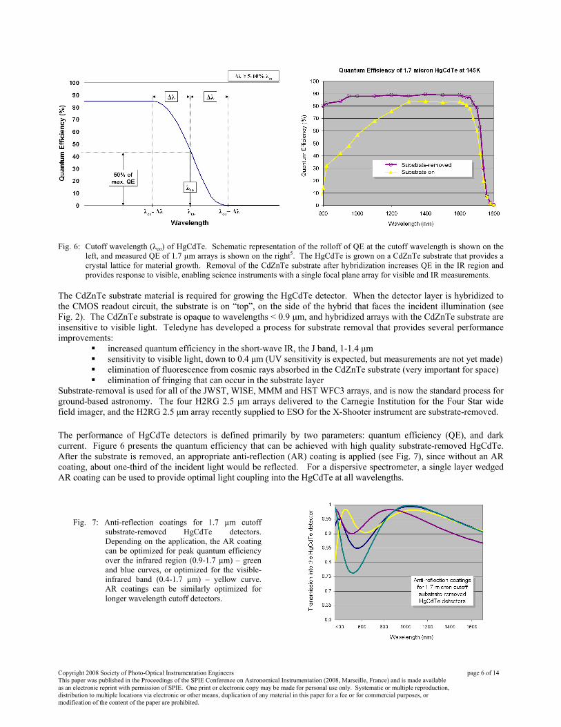
Since the absorption of light near the bandgap is less efficient, the quantum efficiency of a detector layer decreases in the region of the cutoff wavelength as shown in Fig. 6. The industry standard is to define the cutoff wavelength (λco) as the wavelength where the QE is 50% of peak. Technically, this λco does not exactly correspond to the bandgap of HgCdTe mixture, but this definition of λco is a useful parameter for specification of an IR focal plane array. Since the QE starts decreasing at 90-95% of λco, the λco for an astronomy array is usually set at 5-10% beyond the longest wavelength required for science, so that high QE is obtained for all wavelengths of interest. For ground-based telescopes, the standard λco for J & H band is 1.8 µm, the standard for J, H, K is 2.5 µm, and for J through M bands, the standard λco is 5.3 µm.
Copyright 2008 Society of Photo-Optical Instrumentation Engineers This paper was published in the Proceedings of the SPIE Conference on Astronomical Instrumentation (2008, Marseille, France) and is made available as an electronic reprint with permission of SPIE. One print or electronic copy may be made for personal use only. Systematic or multiple reproduction, distribution to multiple locations via electronic or other means, duplication of any material in this paper for a fee or for commercial purposes, or modification of the content of the paper are prohibited.
page 6 of 14
Fig. 6: Cutoff wavelength (λco) of HgCdTe. Schematic representation of the rolloff of QE at the cutoff wavelength is shown on the left, and measured QE of 1.7 µm arrays is shown on the right5. The HgCdTe is grown on a CdZnTe substrate that provides a crystal lattice for material growth. Removal of the CdZnTe substrate after hybridization increases QE in the IR region and provides response to visible, enabling science instruments with a single focal plane array for visible and IR measurements.
The CdZnTe substrate material is required for growing the HgCdTe detector. When the detector layer is hybridized to the CMOS readout circuit, the substrate is on “top”, on the side of the hybrid that faces the incident illumination (see Fig. 2). The CdZnTe substrate is opaque to wavelengths < 0.9 μm, and hybridized arrays with the CdZnTe substrate are insensitive to visible light. Teledyne has developed a process for substrate removal that provides several performance improvements:
increased quantum efficiency in the short-wave IR, the J band, 1-1.4 μm sensitivity to visible light, down to 0.4 μm (UV sensitivity is expected, but measurements are not yet made) elimination of fluorescence from cosmic rays absorbed in the CdZnTe substrate (very important for space) elimination of fringing that can occur in the substrate layer
Substrate-removal is used for all of the JWST, WISE, MMM and HST WFC3 arrays, and is now the standard process for ground-based astronomy. The four H2RG 2.5 μm arrays delivered to the Carnegie Institution for the Four Star wide field imager, and the H2RG 2.5 μm array recently supplied to ESO for the X-Shooter instrument are substrate-removed.
The performance of HgCdTe detectors is defined primarily by two parameters: quantum efficiency (QE), and dark current. Figure 6 presents the quantum efficiency that can be achieved with high quality substrate-removed HgCdTe. After the substrate is removed, an appropriate anti-reflection (AR) coating is applied (see Fig. 7), since without an AR coating, about one-third of the incident light would be reflected. For a dispersive spectrometer, a single layer wedged AR coating can be used to provide optimal light coupling into the HgCdTe at all wavelengths.
Fig. 7: Anti-reflection coatings for 1.7 µm cutoff substrate-removed HgCdTe detectors. Depending on the application, the AR coating can be optimized for peak quantum efficiency over the infrared region (0.9-1.7 µm) – green and blue curves, or optimized for the visible-infrared band (0.4-1.7 µm) – yellow curve. AR coatings can be similarly optimized for longer wavelength cutoff detectors.

Copyright 2008 Society of Photo-Optical Instrumentation Engineers This paper was published in the Proceedings of the SPIE Conference on Astronomical Instrumentation (2008, Marseille, France) and is made available as an electronic reprint with permission of SPIE. One print or electronic copy may be made for personal use only. Systematic or multiple reproduction, distribution to multiple locations via electronic or other means, duplication of any material in this paper for a fee or for commercial purposes, or modification of the content of the paper are prohibited.
page 7 of 14
Dark current is the flow of charge across the p-n junction under bias in the absence of light. Since it is not possible to distinguish dark current from photocharge and since dark current has a Poisson noise distribution (same as photocharge), very low dark current is required for sensing low flux illumination, typical of astronomy applications. Detectors made in MBE material achieve the lowest dark current of all HgCdTe detectors. Dark current is a function of pixel area, temperature, and cutoff wavelength. Figure 8 presents the dark current that Teledyne has achieved for MBE grown HgCdTe, scaled for an 18 µm square pixel. The benefits of low dark current are twofold: (i) low dark current enables the most sensitive flux measurements to be made at very cold temperatures, (ii) low dark current enables operation at the highest temperature for a given level of performance, decreasing thermal load on the instrument cooling system.
Fig. 8: The dark current of MBE grown HgCdTe detector material. The dark current is shown for an 18 µm pixel and can be scaled
for smaller or larger pixel pitch. The cutoff wavelength (λco) is shown with the approximation symbol, since λco is a function of temperature and there will be slight variation in cutoff wavelength of a HgCdTe detector as it cools.
The photocharge that is generated within the detector diffuses in the charge neutral region of the detector until it encounters the depletion region of a pixel’s p-n junction whose field collects the charge. The detector material can be fabricated as either p-on-n, which is a p-type implant into n-type bulk, or vice versa, n-on-p. In a p-on-n detector, the p-n junctions collect holes, and in n-on-p detectors, the p-n junctions collect electrons. Whether the junction collects holes or electrons, all performance quantities, such as full well and readout noise, are stated in units of electrons. Most of the arrays that Teledyne makes for astronomy are p-on-n architecture, but whether holes or electrons are collected should be transparent to all users. However, the distinction is important for the designers of the CMOS readout circuits, which is the subject of the next section. In summary, the detector material used in infrared image arrays is a key factor in array performance. The two primary measures of performance are quantum efficiency and dark current. The highest performance IR material is HgCdTe that is grown by the MBE process, achieving dark current that is less 0.01 electrons per pixel per second for 2.5 and 5 µm cutoff wavelengths. With substrate removal, the HgCdTe is sensitive to visible light, and high quantum efficiency (>80%) can be achieved for wide bandpass, enabling single focal plane array instruments to provide spectral sensitivity from the ultraviolet through the infrared. Teledyne Imaging Sensors is a leader in the production of high performance MBE grown HgCdTe visible-infrared detectors.

Copyright 2008 Society of Photo-Optical Instrumentation Engineers This paper was published in the Proceedings of the SPIE Conference on Astronomical Instrumentation (2008, Marseille, France) and is made available as an electronic reprint with permission of SPIE. One print or electronic copy may be made for personal use only. Systematic or multiple reproduction, distribution to multiple locations via electronic or other means, duplication of any material in this paper for a fee or for commercial purposes, or modification of the content of the paper are prohibited.
page 8 of 14
4. HIGH PERFORMANCE READOUT INTEGRATED CIRCUITS (ROICs) After the photocharge has been collected into pixels, the charge flows to the ROIC via the indium bump bond. A key aspect of the hybrid CMOS imager architecture is that the ROIC is fabricated with the same equipment that is used for making high performance integrated circuits (ICs, or computer chips). With the highly advanced tools used for IC design, the functionality of the ROIC is limited only by the imagination of the designer and the space constraints of the pixel. Space constraints can be overcome by using finer design rules (which denote the smallest feature that can be made on the ROIC), and ROICs for IR imagers are made in 0.25, 0.18 and 0.13 µm design rules. The most basic functionality of the pixel is charge-to-voltage conversion, and transmission of the voltage signal off-chip. It is also possible to include signal processing within the pixel, such as range detection or background subtraction, and some complex pixel designs developed by Teledyne have incorporated nearly 700 transistors within a pixel. The two imaging parameters that are the most significant drivers for ROIC pixel design are: (a) the expected flux of the illumination, and (b) the readout rate of the focal plane array (FPA). These two parameters define the full well of the pixel, i.e. how much charge must be stored in one integration period, and the noise level of the amplifier that is required for photon noise limited performance. There are three basic types of amplifiers used in CMOS ROIC pixels6, as shown in Fig. 9. These amplifiers provide a range of full well and readout noise performance that can be optimized for a specific application. In astronomy, the source follower is the primary amplifier for long exposure low flux imaging, since the source follower is the lowest power, has minimal amplifier glow and relatively low readout noise. The CTIA is used for some adaptive optics ROICs, such as the new Speedster128 design, and is appropriate for longer wavelength, moderate flux astronomy applications. Typically, the direct injection amplifier is used for terrestrial IR imaging, or for long wavelength IR (13-16.5 µm) Earth observations, such as the Advanced Baseline Imager (ABI) of the next generation GOES-R weather satellite.
Fig. 9: Types of amplifiers used in hybrid CMOS IR FPAs. Readout noise is stated for single correlated double sample (CDS),
which is required for removing the reset noise of the amplifier, which is typically greater than readout noise. There are many variations on these designs that can be optimized for a specific application. Note that the full well and readout noise level are coupled and can vary over a wide range; the values presented above are meant to be representative.
Readout noise is a fundamental, although undesirable, attribute of the charge-to-voltage conversion process. All amplifiers suffer from readout noise, which is a random variation of the output voltage that is independent of the level of charge that is input to the amplifier. A critical, and evolving, aspect of amplifier design is reduction of readout noise. In addition to readout noise, a second noise source becomes important for low noise applications: kTC noise, also called reset noise. This noise is introduced when the charge-integrating capacitance in a pixel is reset to a fixed voltage (the

Copyright 2008 Society of Photo-Optical Instrumentation Engineers This paper was published in the Proceedings of the SPIE Conference on Astronomical Instrumentation (2008, Marseille, France) and is made available as an electronic reprint with permission of SPIE. One print or electronic copy may be made for personal use only. Systematic or multiple reproduction, distribution to multiple locations via electronic or other means, duplication of any material in this paper for a fee or for commercial purposes, or modification of the content of the paper are prohibited.
page 9 of 14
reset voltage) at the start of an exposure. Due to the thermodynamic distribution of the number of electrons on the capacitor, the voltage on the capacitor is not completely defined. As long as a current path is provided (i.e. reset switch closed), electrons are constantly moving on and off the charge-integrating capacitor. When the reset switch is opened, the amount of charge is "frozen" on the capacitor, defining a specific voltage offset for this exposure. The voltage offset varies from reset to reset, with a standard deviation of 50-200 electrons (depending on design, temperature, etc.). This variation is called the “reset noise”. Fortunately, reset noise can be removed using a method called correlated double sampling (CDS). To implement CDS, the imager must take two samples for each frame; the first sample immediately after reset, and the second sample at the end of the integration. Since both samples have the same level of bias induced by reset noise, the difference of the two samples will remove the reset noise. CDS is fundamental to the operation of most types of imaging sensors, including CMOS and CCD sensors. A valuable feature of most CMOS arrays used for infrared astronomy is the ability to reduce readout noise by taking many samples during the exposure. This is possible since the pixel readout is non-destructive and the readout noise is uncorrelated from sample to sample. The simplest approach is to reset the pixel at the start of integration and immediately take several samples that can be averaged to reduce the noise of the reset sample of the CDS. An equal number of samples are taken at the end of the frame and averaged. In this way, the “single CDS noise” will be reduced by the square root of the number of samples (if the readout noise is a white noise process). For example, with 4 samples at the beginning and end of the frame (8 samples total), the single CDS readout noise will be reduced by a factor of 2. This approach is called “Fowler sampling” after Al Fowler and Ian Gatley who first implemented this technique7. There is a slight penalty in exposure time since the duration of the exposure is reduced by half of the time required to take the samples. The exposure time loss can be removed by continually sampling during the exposure, and fitting a slope through the samples, where the slope is due to the average light flux. In addition to providing nearly 100% duty cycle, this approach can be used to identify and reject cosmic ray events8. A good example is JWST, which has a standard exposure time of ~1000 seconds, during which a 2K×2K image will be acquired every 10.6 seconds. NIRSpec will use 88 frames taken over the total exposure time, averaging sets of 4 and slope fitting to the 22 average values. NIRCam will use 48 frames, making 6 sets of 8 frame averages, and slope fit through the average values. By doing this, NIRSpec and NIRCam aim to reduce the single CDS noise of ~16 electrons to total noise of ~6 and ~9 electrons, respectively. After charge-to-voltage conversion, the ROIC multiplexes the voltage signal to the edge of the FPA where it can be read out to off-chip electronics. The multiplexer can be designed to quickly read out windows in the array, or to subsample (e.g. every other pixel and every other row), or almost any other imaginable mode of operation. At the system level, it is critical to clearly define the complete concept of operations of the instrument and the FPA at the beginning of a development program. An operation mode that is relatively easy to implement at the initial design stages can become very hard, if not impossible, to implement at an advanced stage of development. The last step in digital imaging is conversion of the analog voltage to a digital value. For Teledyne’s imaging sensors, analog-to-digital converters (ADCs) are typically provided in the following resolutions / conversion rates: 12 bit / 40 MHz, 14 bit / 20 MHz, 16 bit / 500 kHz. The power of ADCs continues to drop so that ADCs can now be integrated into the ROIC without significant additional heat load. For the highest performance ADCs, the power expended is 1-2 mW per MHz for a 12-bit ADC, 3-5 mW per MHz for a 14 bit ADC, and 3 mW per 100 kHz for a 16-bit ADC. 4.1 The Hawaii-2RG (H2RG) ROIC The H2RG is the most prominent member of the evolving HAWAII family of infrared imaging arrays produced by Teledyne Imaging Sensors for astronomy. HAWAII is an acronym for HgCdTe Astronomical Wide Area Infrared Imager, and other members of the HAWAII family are the H1, H1R, H1RG, and H2. For these arrays, the H stands for HAWAII, the number 1 or 2 denotes 1024×1024 or 2048×2048 pixels, R denotes reference pixels, and G denotes guide window capability. The reference pixel and guide mode features are explained below. A large number of H1 and H2 arrays are in use at ground-based observatories. The H1R flew on the Deep Impact asteroid intercept mission and is integral to the Wide Field Camera 3 (WFC3) being installed in the Hubble Space Telescope (HST) in October 2008. The H1RG array is being used in the Orbiting Carbon Observatory (OCO) and the Wide-field Infrared Survey Explorer (WISE) that will launch in 2009 to provide an all-sky 3.5-23 μm infrared survey.
Copyright 2008 Society of Photo-Optical Instrumentation Engineers This paper was published in the Proceedings of the SPIE Conference on Astronomical Instrumentation (2008, Marseille, France) and is made available as an electronic reprint with permission of SPIE. One print or electronic copy may be made for personal use only. Systematic or multiple reproduction, distribution to multiple locations via electronic or other means, duplication of any material in this paper for a fee or for commercial purposes, or modification of the content of the paper are prohibited.
page 10 of 14
The CMOS readout circuit for the H2RG provides several advanced performance features:
Reference pixels: There are four rows and columns of reference pixels along each side of the array. These reference pixels track any bias voltage fluctuations over the long (typically 1000 second) exposures required in astronomy. Reference pixel subtraction is essential to achieve the lowest noise performance.
Guide window: The H2RG can intersperse readout of a guide window with readout of the entire array, so that the science array can perform the guiding function required for accurate telescope stabilization.
Low noise from non-destructive readout and multiple sampling: The pixel amplifier in the H2RG is read out non-destructively, and during a long exposure a large number of sub-frames can be read out and slope fit to reduce the single CDS noise. Total noise is a combination of readout noise and dark current noise, and 6 electrons total noise for a 1000 sec exposure defines the state-of-the-art.
Very low power operation: To read out the H2RG with four readout ports, each at 100 kHz pixel rate (10.6 sec full frame readout), the H2RG requires less than 1 mW power.
Elimination of amplifier glow: Current that flows through the amplifier in the pixel of the CMOS readout array can produce infrared photons that result in an undesired background glow. The H2RG has effectively eliminated amplifier glow by readout circuit design and light shielding with metal layers, which enables the extremely low noise that is achieved by multiple non-destructive readout.
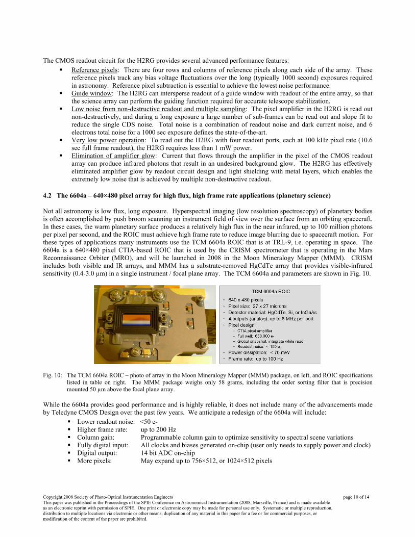
4.2 The 6604a – 640×480 pixel array for high flux, high frame rate applications (planetary science) Not all astronomy is low flux, long exposure. Hyperspectral imaging (low resolution spectroscopy) of planetary bodies is often accomplished by push broom scanning an instrument field of view over the surface from an orbiting spacecraft. In these cases, the warm planetary surface produces a relatively high flux in the near infrared, up to 100 million photons per pixel per second, and the ROIC must achieve high frame rate to reduce image blurring due to spacecraft motion. For these types of applications many instruments use the TCM 6604a ROIC that is at TRL-9, i.e. operating in space. The 6604a is a 640×480 pixel CTIA-based ROIC that is used by the CRISM spectrometer that is operating in the Mars Reconnaissance Orbiter (MRO), and will be launched in 2008 in the Moon Mineralogy Mapper (MMM). CRISM includes both visible and IR arrays, and MMM has a substrate-removed HgCdTe array that provides visible-infrared sensitivity (0.4-3.0 µm) in a single instrument / focal plane array. The TCM 6604a and parameters are shown in Fig. 10.
Fig. 10: The TCM 6604a ROIC – photo of array in the Moon Mineralogy Mapper (MMM) package, on left, and ROIC specifications listed in table on right. The MMM package weighs only 58 grams, including the order sorting filter that is precision mounted 50 µm above the focal plane array.
While the 6604a provides good performance and is highly reliable, it does not include many of the advancements made by Teledyne CMOS Design over the past few years. We anticipate a redesign of the 6604a will include:
Lower readout noise: <50 e- Higher frame rate: up to 200 Hz Column gain: Programmable column gain to optimize sensitivity to spectral scene variations Fully digital input: All clocks and biases generated on-chip (user only needs to supply power and clock) Digital output: 14 bit ADC on-chip More pixels: May expand up to 756×512, or 1024×512 pixels

Copyright 2008 Society of Photo-Optical Instrumentation Engineers This paper was published in the Proceedings of the SPIE Conference on Astronomical Instrumentation (2008, Marseille, France) and is made available as an electronic reprint with permission of SPIE. One print or electronic copy may be made for personal use only. Systematic or multiple reproduction, distribution to multiple locations via electronic or other means, duplication of any material in this paper for a fee or for commercial purposes, or modification of the content of the paper are prohibited.
page 11 of 14
5. SIDECARTM ASIC – FOCAL PLANE ELECTRONICS IN A SINGLE INTEGRATED CIRCUIT In parallel with the development of the H2RG, Teledyne developed an application specific integrated circuit (ASIC) that interfaces directly with the H1RG and H2RG and provides all of the functionality required from focal plane electronics (FPE). The SIDECAR (System for Image Digitization, Enhancement, Control and Retrieval) ASIC, shown in Fig. 11, provides significant reduction in the size, weight and power of the FPE9. The SIDECAR contains a programmable microprocessor, bias generators, clock generators, amplifiers and analog-to-digital converters (ADCs). Up to 36 analog inputs can be accommodated in parallel, with choice of 500 kHz, 16-bit ADC or 10 MHz, 12-bit ADC (36 ADCs operate in parallel). The SIDECAR presents a digital interface to instrument electronics, and with LVDS (low voltage differential signal) communication, the SIDECAR can be placed several meters from the instrument electronics. All operation of the SIDECAR is fully programmable via LVDS communication lines. The SIDECAR ASIC has been selected for use in 3 of the 4 instruments of the JWST. Two features of the SIDECAR were important factors in its selection for JWST:
1. Low power operation: For JWST operation - 4 ports continuously read at 100 kHz pixel rate and 16 bit digitization - the SIDECAR uses 11 mW power at 37K. The low power operation enables JWST to place the SIDECAR within the very cold (37K) instrument module which is located 4 meters cable length from the electronics located in the warm section of the observatory.
2. Low noise performance: The SIDECAR noise is negligible when compared to the H2RG readout amplifier, so that the total noise of the H2RG-SIDECAR system is set by the low noise H2RG operation.
The SIDECAR ASIC was also selected for the repair of the Advanced Camera for Surveys (ACS) instrument in the Hubble Space Telescope. In this system, the SIDECAR will be used to operate two 4K×2K CCDs. The ACS Repair will take place during HST Servicing Mission 4, which is scheduled for October 2008. For the ACS Repair, a new hermetically sealed spaceflight package was developed for the SIDECAR ASIC. The SIDECAR ASIC packaging is shown in Fig. 11.
Fig. 11: SIDECAR ASIC and its packages. The ground-based astronomy package (left), the Hubble Space Telescope hermetically
sealed package (center), and the James Webb Space Telescope cryogenic package (right). Both the H2RG and the SIDECAR have undergone environmental testing in spaceflight packages and have been demonstrated to NASA’s Technology Readiness Level 6 – an important milestone for acceptance in space missions. Both the H2RG and the SIDECAR have shown a high level of radiation hardness, and are now being considered for other space missions. The SIDECAR has been operating the 4096×4096 pixel infrared camera (mosaic of four H2RGs) at the University of Hawaii 88-inch telescope since early 2007, and the SIDECAR is being incorporated into new instruments for several ground-based observatories, including, but not limited to: Carnegie Observatory (Four Star) wide field imager, W.M. Keck Observatory (MOSFIRE multi-object spectrograph being developed by UCLA), Carnegie Observatory (FIRE spectrograph being developed by MIT), Subaru Telescope (HiCIAO imager being developed with U. Hawaii), Gemini Observatory (Gemini Planet Imager instrument being developed by UCLA).

Copyright 2008 Society of Photo-Optical Instrumentation Engineers This paper was published in the Proceedings of the SPIE Conference on Astronomical Instrumentation (2008, Marseille, France) and is made available as an electronic reprint with permission of SPIE. One print or electronic copy may be made for personal use only. Systematic or multiple reproduction, distribution to multiple locations via electronic or other means, duplication of any material in this paper for a fee or for commercial purposes, or modification of the content of the paper are prohibited.
page 12 of 14
6. SPACEFLIGHT FPA PACKAGING The 5-10 µm thick HgCdTe detector layer is only a few milligrams, but it must be positioned at precisely the right location for light to be properly focused and detected. The tolerance on FPA packaging can be as small as a few µm and the package must simultaneously provide thermal management and withstand the environmental stress of launch. Additionally, for very large focal plane arrays, multiple arrays must be mosaicked to high precision to provide a large focal plane area.
A key aspect of FPA packaging is thermal management. One example is the Fine Guidance Sensor (FGS) used on the James Webb Space Telescope (JWST) to provide optical pointing stability. Developed with the financial support of the Canadian Space Agency, the FGS package, shown in Fig. 12, has been assembled and the engineering unit has been delivered to Com Dev, the FGS instrument integrator. During vibration tests, the resonance frequency matched the predicted performance to within 5%, and the thermal design has also been demonstrated. The temperature of the imaging array can be stabilized to 1 mK while the temperature of the cold thermal strap to the focal plane assembly varies by as much at 5 K. The FGS package is now rated TRL-6.
Many proposed space astronomy programs involve large surveys that will measure over 100 million galaxies or stars. The large number of measurements is required to provide the statistical information required to map the dark matter and dark energy in the universe, and to find planets around other stars. While the size of individual arrays continues to grow, the very large focal plane arrays required for many space missions will only be achieved by mosaicking a large number of individual arrays. An example of a large mosaic is shown in Fig. 12, which presents a 147 megapixel focal plane array that is comprised of 35 H2RG arrays (each with 2048×2048 pixels). Teledyne Imaging Sensors has significantly increased its capabilities in spaceflight packaging and has produced many custom packages for ground and space applications. Four examples are shown in Fig. 12.
Fig. 12: Examples of Teledyne Imaging Sensors packaging: (top left) Orbiting Carbon Observatory H1RG - visible and IR arrays,
(top right) JWST Fine Guidance Sensor package for the H2RG, (bottom left) a mosaic of four H2RGs as is being used by ESO, CFHT, and other ground-based observatories, (bottom right) a mechanical prototype of a mosaic of 35 H2RG arrays as envisioned for the Microlensing Planet Finder.

Copyright 2008 Society of Photo-Optical Instrumentation Engineers This paper was published in the Proceedings of the SPIE Conference on Astronomical Instrumentation (2008, Marseille, France) and is made available as an electronic reprint with permission of SPIE. One print or electronic copy may be made for personal use only. Systematic or multiple reproduction, distribution to multiple locations via electronic or other means, duplication of any material in this paper for a fee or for commercial purposes, or modification of the content of the paper are prohibited.
page 13 of 14
7. NEXT GENERATION OF DETECTORS – NEW DEVELOPMENTS UNDERWAY Teledyne Imaging Sensors continues to develop new types of IR arrays for a wide variety of customers. In the astronomy area, two new arrays are in development:
Speedster128 – 128×128, 40 µm pixel high speed, low noise array for adaptive optics and interferometry H4RG-15 – 4096×4096, 15 µm pixel array for future infrared astronomy instrumentation
7.1 Speedster128 – high speed, low noise array for adaptive optics and interferometry The Speedster128 array is designed to serve the needs of IR wavefront sensing and fringe detection. Production has commenced on the readout circuit, and the first visible and IR arrays will be fabricated in 2008. The Speedster128 array is optimized for fast readout of small charge packets with lowest possible noise. Each pixel has a capacitive transimpedance amplifier (CTIA) that is designed for highest responsivity, enabling readout noise of less than 5 electrons at 900 Hz frame rate. There is a CDS circuit within each pixel so that the multiplexer output is a CDS signal. The array provides 100% duty cycle with a snapshot, integrate-while-read design. The Speedster128 array has a relatively simple readout mode – all pixels are read out every frame. An application that only requires a subset of pixels can capture the pixels of interest as the data is read off the chip. The Speedster128 can be supplied with a computer interface board that provides analog-to-digital conversion and interfaces directly to commercial off-the-shelf frame grabbers. Fig. 13 provides a diagram of the Speedster128 and main attributes. Fig. 13: Speedster128 ROIC that is optimized for high speed, low noise readout. Devices being fabricated during 2008 include
visible silicon PIN detectors, 1.8 µm IR arrays, and 2.5 µm IR arrays. 7.2 H4RG-15 - The next generation IR array for future instrumentation, telescopes and space missions The H2RG-18 is the ROIC and FPA format of choice for many new instruments and proposed space missions since the performance has been demonstrated on many operating instruments, and the H2RG-18 has achieved TRL-6. Future instruments and space missions, including the Extremely Large Telescopes, will require very large focal plane arrays with hundreds of millions of pixels. To enable next generation instrumentation to be affordable, it will be important for the cost per pixel of infrared arrays to be significantly reduced below the present price. With the maturation of the H2RG into a production array, it is now feasible to increase the pixel count per array by a factor of four to produce a 4096×4096 pixel IR array in a single device. To make the 4K×4K array practicable, the pixel pitch should be reduced to 15 µm. From our conversations with instrument designers, systems engineers and manufacturing engineering, it appears that the 6×6 cm (4K×4K, 15 µm) IR hybrid size provides the optimal tradeoff of performance, manufacturability and instrument design constraints. Our plan is to develop a silicon carbide (SiC) package for the H4RG-15, since SiC provides a lightweight package with excellent thermal properties. The thermal conduction of SiC is relatively high, and SiC provides a good match to the coefficient of thermal expansion (CTE) of the silicon ROIC. The size of the H4RG-15 pixel array is big enough to embed the SIDECAR ASIC directly within the package. Operating the SIDECAR with 32 ports in parallel, at 100 kHz

Copyright 2008 Society of Photo-Optical Instrumentation Engineers This paper was published in the Proceedings of the SPIE Conference on Astronomical Instrumentation (2008, Marseille, France) and is made available as an electronic reprint with permission of SPIE. One print or electronic copy may be made for personal use only. Systematic or multiple reproduction, distribution to multiple locations via electronic or other means, duplication of any material in this paper for a fee or for commercial purposes, or modification of the content of the paper are prohibited.
page 14 of 14
readout rate and 16 bit digitization will require 120-150 mW of power. If this amount of power is too high for close proximity to the focal plane, the package will also provide an analog output that can interface to the SIDECAR ASIC which is placed in a different thermal environment, although still close to the image array. A drawing of the package is shown in Fig. 14.
Fig. 14: H4RG-15 IR array - the next generation in infrared astronomy. From left to right, the images show the light sensitive HgCdTe layer, the bottom of the silicon carbide package with analog outputs, the SiC package with embedded SIDECAR ASIC, and the bottom of the embedded SIDECAR ASIC package with digital output.
8. SUMMARY
Teledyne Imaging Sensors (TIS) is strongly committed to providing the highest performance infrared arrays to the astronomical community. Key to high performance is high quality HgCdTe detector material that achieves high quantum efficiency (>80%) over a wide bandpass and very low dark current (<0.01 e-/pix/sec). TIS offers readout circuits that provide low noise readout for both long exposure, low light level astronomical instrumentation, and high frame rate adaptive optics systems. TIS’s leading image array is the H2RG-18, which is being used by nearly all leading ground-based observatories and the James Webb Space Telescope. The focal plane electronics for the H2RG is provided by the SIDECAR ASIC, which is a compact, low power, cryogenic chip that significantly reduces system complexity. Both the H2RG and SIDECAR are rated TRL-6, and are ready for spaceflight. TIS continues to develop new arrays for astronomy. The Speedster128 array (128×128 pixels) provides high speed (900 Hz frame rate), low noise (5 e- single read) performance for adaptive optics and inteferometry. A new large IR array is in development; the H4RG-15 (4096×4096, 15 µm pixel) has been designed and initial production of infrared arrays should commence in 2008.
REFERENCES [1] Beletic, J.W., “IR imaging arrays enable imaging that is out of this world”, Laser Focus World, 75-78, (Oct. 2007). [2] Sprafke, T. and J.W. Beletic, “High Performance Focal Plane Arrays for Space Applications”, Optics and Photonics
News, 22-27, (June 2008). [3] Bai, Y., J. Bajaj, J.W. Beletic, M.C. Farris, A. Joshi, S. Lauxtermann, A. Petersen, and G. Williams, “Teledyne
Imaging Sensors: Silicon CMOS imaging technologies for x-ray, UV, visible and near infrared”, Proceedings of the SPIE, Vol. 7201, (June 2008).
[4] Hansen, G.L., J. L. Schmidt, T. N. Casselman, “Energy gap versus alloy composition and temperature in Hg1-xCdxTe ”, J. Appl. Phys. 53(10), p. 7099, (1982).
[5] Piquette, E.C., D.D. Edwall, H. Arnold, A. Chen, and J. Auyeung, “Substrate Removed HgCdTe-Based Focal Plane Arrays for Short Wavelength Infrared Astronomy”, Journal of Electronic Materials, SpringerLink, (2008).
[6] Hoffman, A., M. Loose, and V. Suntharalingham, “CMOS Detector Technology”, pp. 377-402, in Scientific Detectors for Astronomy 2005, edited by Beletic, J.E., J.W. Beletic, and P. Amico, Kluwer, (2006).
[7] Fowler, A.M., and I. Gatley, “Demonstration of an algorithm for read-noise reduction in infrared arrays,” Astrophys. J. 353:L33-L34, (1990).
[8] Offenberg, J. D., Sengupta, R., Fixsen, D. J., Stockman, H. S., Nieto-Santisteban, M. A., Stallcup, S., Hanisch, R. J., & Mather, J. C., “Cosmic Ray Rejection with NGST”, in ASP Conf. Ser., Vol. 172, Astronomical Data Analysis Software and Systems VIII, eds. D. M. Mehringer, R. L. Plante, & D. A. Roberts (San Francisco: ASP), 141, (1999).
[9] Loose, M., J.W. Beletic, J. Blackwell, D. Hall, and A. Jacobsen, “SIDECAR ASIC – Control Electronics on a chip”, pp. 699-706, Scientific Detectors for Astronomy 2005, editors Beletic, J.E., J.W. Beletic, P. Amico, Kluwer, (2006).
This paper has been approved for public release by the DoD Office of Security Review (case #08-S-1729).