technology scaling at an inflection point what’s next?
TRANSCRIPT

Technology scaling at an inflect ion pointTechnology scaling at an inflect ion point
W HAT’S NEXT?Lode Lauw ers I MECLode Lauw ers, I MEC
1imec confident ial 2009
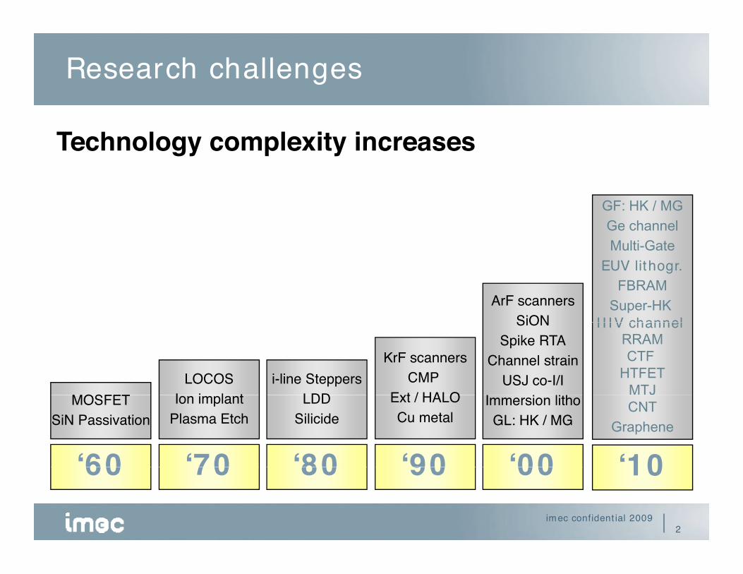
Research challenges
Technology complexity increases
*)��+.���0**H�FKDQQHO0XOWL�*DWH
ArF scannersSiON
0XOWL *DWHEUV lithogr.
)%5$06XSHU�+.
I I I V channel
MOSFETLOCOS
I i l ti-line Steppers
LDD
KrF scannersCMP
Ext / HALO
SiONSpike RTA
Channel strainUSJ co-I/I
I i li h
I I I V channel55$0&7)
+7)(707-MOSFET
SiN PassivationIon implant
Plasma EtchLDD
SilicideExt / HALOCu metal
Immersion lithoGL: HK / MG
‘70 ‘80 ‘90 ‘00‘60
&17*UDSKHQH
‘10
2imec confident ial 2009
70 80 90 0060 10

CMOS scaling roadm ap
Scaling
TunnelFETActive Area
Gate FieldSpacers
Active Area
Gate FieldSpacers
Active Area
Gate FieldSpacers
Ge/IIIVGe/IIIV
nanowiresnanowires
graphenegraphene
ArF + RETArF + RET
ArF immersionArF immersion
CNT’sCNT’sGe/IIIVGe/IIIV
metal gatemetal gate
FinFETFinFET
22nm
< 15 nm
2L=35nm
SiGe
L=35nmL=35nm
SiGe
strainstrain
HfOhigh high --NN
metal gatemetal gate
45-32nm
22nm
DoublePatterning
ili idili id
USJUSJ
strainstrain
> 65nm
3imec confident ial 2009
time EUVLsilicidesilicide

I MEC FEOL Research Topics & Roadm ap
L i HKMG Super-HK I I I -V channelsHTFETLogic
SRAMHKMG
m -sec anneal Ge channelsMult i-Gate
HTFETMTJ
FBRAM
DRAM MI M: K> 50CoSi
MI M: K> 80HKMG
Mult i-GateMI M: K> 80, Ru
FBRAM
FG: HK I PD CTF: HK BO RRAMProbe m em oryFG: MG
FG: float ing gateNVM CTF: MG
CTF: SiN+
Probe-m em oryGraphene
Mot t Transit ion
4imec confident ial 2009
< 2y 2-5y > 5y

CMOS scalingCNT
ii
graphenegrapheneAir gap
3 D TSV
FinFETFinFET
Active Area
Gate FieldSpacers
Active Area
Gate FieldSpacers
Active Area
Gate FieldSpacers
Ge/IIIVGe/IIIV
nanowiresnanowires
Low kk= 2 .2 …
3 D SI P3 D SI P
25 nm25 nm
HfO2high high --NN
metal gatemetal gate
FinFETFinFET
Low kk= 3 .0
Low kk= 2 .7 - 2 .5
L=35nm
SiGe
L=35nmL=35nm
SiGe
NiSiNiSi
FUSIFUSI
strainstrain
Cu
strainstrain
USJUSJ
silicidesilicide
5imec confident ial 2009
timesilicidesilicide

3D @ I MECProgram components X= SDR or partner vehicle
Circuit & System demonstrations
3D-Systemdemonstrators
Design & Technology Demonstration
3D SDR
W P3 :
W P4 :3 D System Explorat ion
3D config able
3D (System )Design Flow
W P5 : 3 D System s
Program components2: Mod
el
X’System
X’ Design
X’I P
X= SDR or partner vehicle
3D-SOC3D-Sensors3D-chip stacks
g gy
3 D Technology
W P3 :I P/ Macros for 3 D
W P1 :Design k it for 3 D
3D DRAM 3D configurable memory
CAD
DRC LVS XRCDRM
TSV models
Reliability
3D NoC
WLP SI C
...
...
.. .
WP2
Cost
M
X’ Flow
X’I P
Signal I ntegrity
3D-WLP 3D-SIC 3D-IC
Design ExplorationEnable system design and prototyping with 3D TechnologiesEnable system design and prototyping with 3D Technologies
Technology Development
2nd stacked die
3rd stacked die
Carr ier die
2nd stacked die
3rd stacked die
Carr ier die
6imec confident ial 2009Landing die
1st stacked die
Landing die
1st stacked die
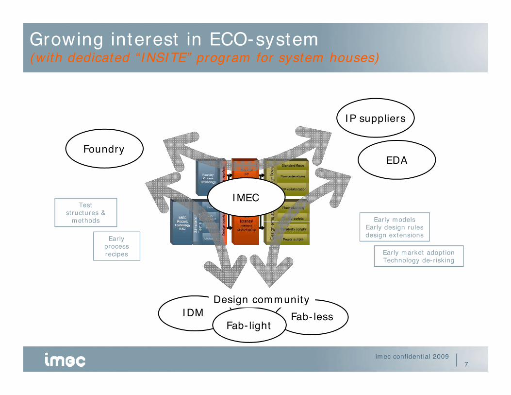
Growing interest in ECO-system(with dedicated “ I NSI TE” program for system houses)
I P suppliers
Foundry
pp
EDA
Testst ructures &
m ethods Early models
I MEC
Earlyprocessrecipes
m ethods yEarly design rulesdesign extensions
Early m arket adopt ionTechnology de- r isking
Fab- lessI DMF b li h
Design com m unity
7imec confident ial 2009
Fab- light
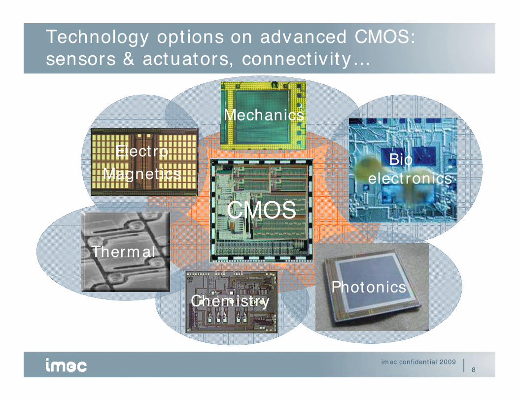
Technology opt ions on advanced CMOS:sensors & actuators, connect ivity…
Mechanics
Elect roMagnet ics
Bioelect onics
CMOSMagnet ics elect ronics
Therm al
PhotonicsChem ist ry
8imec confident ial 2009

9imec confident ial 2009

FEO
L D
evic
e FE
OL
Dev
ice
Stra
tegy
Map
Stra
tegy
Map
200/
300m
m P
ilot L
ine
Rou
tes
optim
ized
for:
-Fle
xibi
lity
(mat
eria
ls, d
evic
es)
-Cyc
le ti
me
-Qua
lity
of P
roce
ssin
g
R
D
D
M
Logi
cLo
gic
DR
AM
DR
AM
Flas
hFl
ash
D
DD
F
SIT
F
F
CR
RPG
DMG (Bulk
DMG (SOI F
MIMCAP
DMG (Bulk
D40: PolyD30: DMG
Floating
SiGe/Ge II-V chan
TFET fam
FBC
FBC
Charge TRRAM
Cha
nnel
Silic
ide
CMOS)
FinFET)
FinFET)
y-Si (Peri)
G (Peri Plana
Gate
channelnnelmily
Trap
TUSJ
ar)
Circ
uit
Tox
10im
ec c
onfid
entia
l 200
9D
evic
e R
esea
rch
Plat
form
Dev
ice
Res
earc
h Pl
atfo
rm
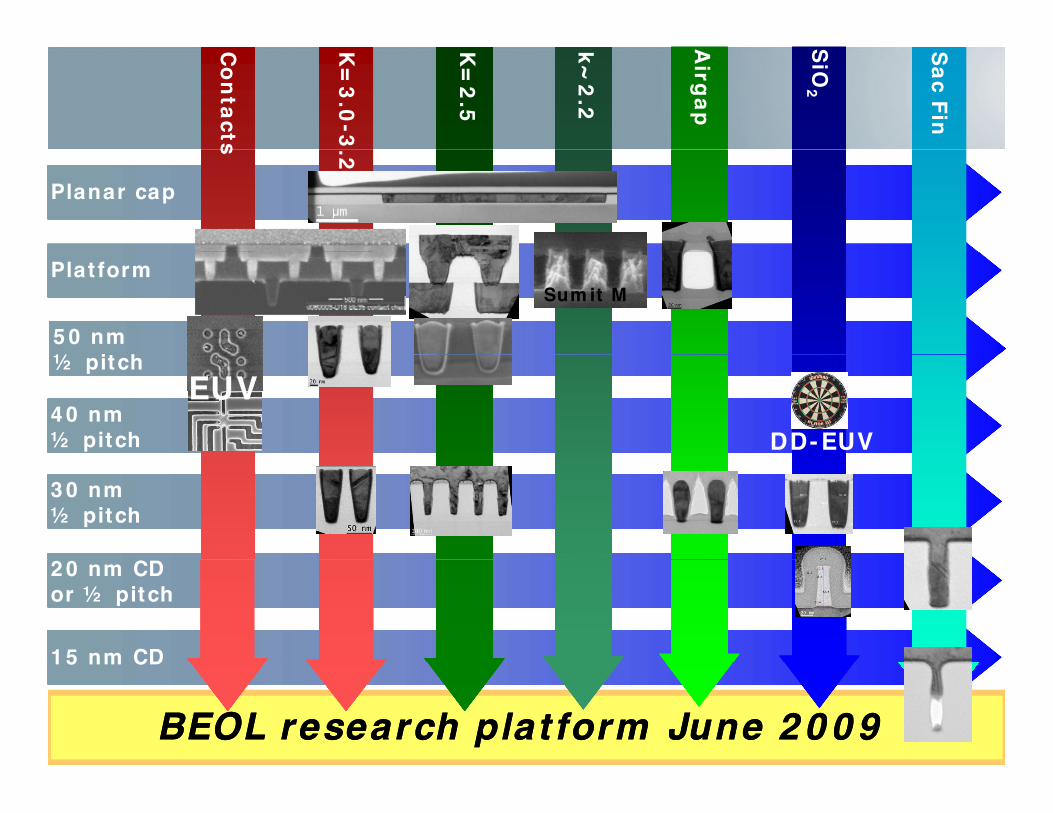
Contacts
K=
3.0-3
K=
2.5
Sac Fin
k~2.2
Airgap
SiO2
Planar cap
s .2
Plat form
5 0 nm½ it h
Sum it M
4 0 nm½ pitch
½ pitchEUV
DD- EUV
3 0 nm½ pitch
1 5 nm CD
2 0 nm CD or ½ pitch
11imec confident ial 2009
1 5 nm CD
BEOL research plat form June 2 0 0 9 BEOL research plat form June 2 0 0 9

I ncreasing link Technology-design
I ntegrated Solut ions for Technology Explorat ion ( I nsite)
Exploring em erging patterning technologiesat system / SOC level
Tool and m ethodologies to explor ing em erging devices
at system / SOC level
Lithography FEOL cluster I nterconnect Cluster
3DP3DIHy
Im Lo CuDo
Pa
EU
Em
NV
a t system / SOC level
D W
LP
Post-foundry T
D SIC
n-foundry TSV
yper NA
m
mersion
ogicDram
u/Low k
oubleatterning
UV
L
merging D
ev
V-M
emory
TSV &
stacking
V Technology
vices
g
Support ing Expert ise Centers
Mater ialsCharacterizat ion
Reliability, ESD, TCADAdv. Character izat ion
Unit Processes Research( Clean/ Str ip, Epi, ALD, ( D) RI E, Ab I nit io
T t d li
12imec confident ial 2009
Characterizat ion& Metrology
Adv. Character izat ion( Fill & Sense…)
( Clean/ Str ip, Epi, ALD, ( D) RI E, anneal, m etallizat ion…) Transport m odeling