technical report - iuac, new delhi, india · arti gupta1, s.venkataramanan2 , ... technical report...
TRANSCRIPT

TECHNICAL REPORT
TITLE :Technical Report on Shaping Amplifier for Neutron Detector Array
AUTHORS : Arti Gupta, S.Venkataramanan, K.S. Golda R. K. Bhowmik
CATEGORY : Instrumentation
REFERENCE NO : NSC/TR/AG/2006-07/
INTER UNIVERSITY ACCELERATOR CENTRE(An Autonomous Inter-University Centre of UGC)
Post Box No.: 10502, Aruna Asaf Ali Marg,New Delhi 110067 (India) Phone: 2689 3955, 2689 2603, 2689 2601
Fax: 091-11-2689 3666 Email: [email protected]

Technical Report on Shaping Amplifierfor Neutron Detector Array
CONTENTS1. Abstract
2. Acknowledgment
3. Specifications
4. Introduction
5. Principle of operation
6. Test Results
7. Troubleshooting Procedure
8. Assembly Procedure
9. Conclusion
10. References
11. Photographs
12. Block Diagram
13. Bill of material
14. Schematic diagram
15. Annexture 1.1 and 1.2
16. PCB artwork TOP, BOTTOM layers
17. Silk screen TOP, BOTTOM layers
18. Drill drawing
Prepared by
ELECTRONICS LABORATORYINTER UNIVERSITY ACCELERATOR CENTRE,
P.B.10502, NEW DELHI 110067.

Technical Report on Shaping Amplifierfor Neutron Detector Array
Arti Gupta1, S.Venkataramanan2 , K.S. Golda, R. K. Bhowmik
Electronics Laboratory, Inter University Accelerator Centre, P.B.10502, Aruna Asaf Ali Marg,
New Delhi 110067 1,2email: arti @iuac.ernet.in, [email protected]
Abstract
As a part of the on going nuclear electronics development activities for
Neutron Detector Array at IUAC, we have developed a high density Spectroscopy
amplifier. It is designed with fixed Pole-zero correction, 1µs shaping time constant
and gain ranging from ~ 0.25 to 10. It accepts negative pulses from the preamplifier
and gives bipolar output. Linearity of the amplifier is compared with ORTEC 572
amplifier using Canberra Pulser (model 8210). The principle of operation of various
circuit blocks are explained in this report along with representative test point signals
which will be very useful for troubleshooting. The amplifier specifications and test
results are also given.
Acknowledgment
We would like to thank Dr R.K. Bhowmik of IUAC for evaluating the
performance of the amplifier. We also would like to thank Apprentice trainees
participated during assembling. Our sincere thanks to Dr. Amit Roy, and B.P. Ajith
Kumar, for their constant encouragement and providing necessary infrastructure in
order to complete this project successfully.

Specifications: Shaping Amplifier for Neutron Detector Array
Input impedance : ~1k
Input Signal and Signal range : -ve pulses with decay time ~50s, ± 1V
Output impedance : 10
Output Signal and Signal range : Bipolar, ± 10V Active filter shaped
FWHM : 2.09keV (122keV), 5.3keV (1408 keV) of
152Eu
Gain : ~10, Inverting type
Fine Gain : ~ x0.025 to x1 (Front Panel Potentiometer)
Input attenuator : x0.4, x0.7 and x1 (On-board Jumpers)
Pole/Zero : Fixed for input pulse with decay time ~50µS
Shaping time & type : 1 µS Fixed
Power required : +/- 6V, +/- 20mA
: +/- 12V, +/- 45mA
Size (W x H x L) : 1.5” x 0.6” x 1.9”

Introduction A Shaping amplifier with fixed pole-zero correction and 1us shaping time
constant has been developed for Neutron Detector Array at IUAC and is being used
as a daughter card of “Pulse Shape Discriminator Electronics Module”. It essentially
consists of input attenuator, fine gain control, differentiation stage with Pole-Zero
(P/Z) compensation, gain stages, active shaping followed by 2nd differentiation stage
for bipolar output and output amplifier. Three on-board jumpers have been provided
to select the attenuation factor i.e. x1, x0.7 and 0.4. Amplifier Gain can be adjusted
by front panel potentiometer in the range of ~ 0.25 to 10. The output Bipolar output
was chosen for convenience in zero crossover timing applications. A block diagram
has been attached for quick reference.
The amplifier is assembled as a daughter card of “Pulse Shape Discriminator
Electronics Module” on a double sided glass epoxy PCB with surface mount
components to achieve the required high density.
Principle of Operation The amplitude of the pulses from Neutron detector preamplifier range from
few 100mV to 5.5V with decay time of 50µS. To handle such a large signal we have
put 3 stage on-board jumper selectable attenuator network. This is followed by four
quadrant analog multiplier U3 (AD835) which is being used to control the fine gain
of the amplifier from 0.025 to 1. AD835 inputs are rated for +/- 1V maximum so a
protection circuit is added at its input to prevent voltage excursions greater than 1V
in magnitude. The early differentiation is done with passive RC components for 1µS
(C5, R14). The Pole-Zero(P/Z) correction is done with (R10, C5).
The differentiated pulse is amplified with low noise high quality operational
amplifier (U2). This stage is wired with clamping circuit in feedback path to speedup
overload recovery. The amplified pulses are shaped with, 2 stages of 2nd order active
integration (U1 A&B) and one stage of differentiation (C19, R31), where RC
components are chosen for required shaping time constant of 1µS, to get bipolar
output. This is further followed by an output amplifier stage in closed loop with push-
pull buffer to improve the current driving capability of the amplifier.

Test ResultAs a preliminary test, linearity of the IUAC amplifier is compared with
ORTEC 572 amplifier using Canberra Pulser model 8210. Linearity graph (FIG.1)
have been attached for reference. Later on it was tested with liquid scintillator (BC
501). Testing has been carried out with different γ-sources to ensure the linearity of
the amplifier. FIG.2 shows a typical energy spectrum obtained with 137Cs neutron
source. The gain of the amplifier is adjusted in such a way that the neutron energy
region of our interest would fall well within the dynamic range of the amplifier.
FIG 1: Linearity error of IUAC amplifier w.r.t. ORTEC 572 amplifier at
specified output voltages using Canberra Pulser Model 8210.

FIG 2. Energy Calibration:
Commercial: Ortec 572 amplifier, Bi Out, 1uS, (X6.5), Source: Cs137 (662 keV)IUAC: Bi-Out, 1uS, Coarse MiddleCalibration: 0.57 keV/channel
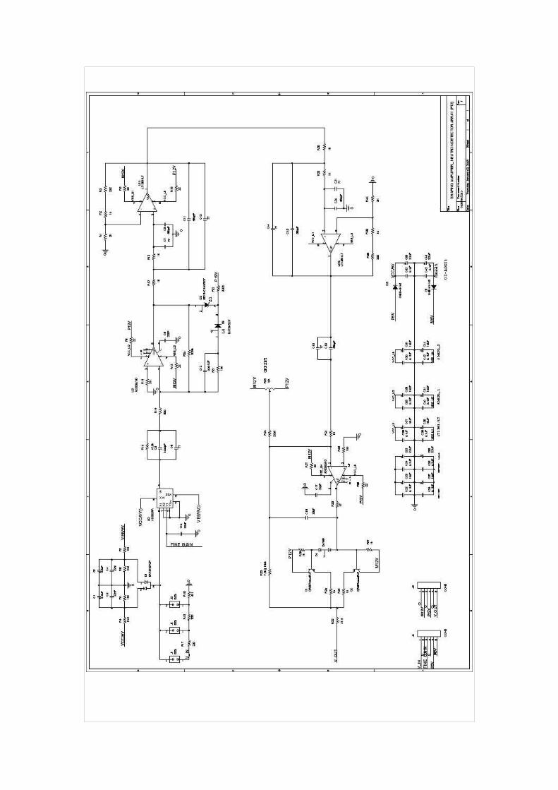
Troubleshooting Procedure1. Ensure that +/-12V and +/-6V supplies are not grounded anywhere on the
PCB.
2. Insert the card in the respective slot on the mother board.
3. Provide power connections to the module. Confirm that +/-12V and +/-6V are
reaching the board.
4. Refer the Shaper schematic diagram showing dc conditions of the circuit to
check dc voltages at various points in the circuit. (Annexure 1.1)
5. Apply negative input signal to DYNODE input on the back panel of the PSD
module using BNC pulser model DB-2 (Vin= -1V, Tr=100nS, Td= 50uS).
6. Follow the schematic diagram with waveform representation to check signals
at various points in the circuit. (Annexure 1.2)
Assembly ProcedureThe currently (Shaper_PT2/Aug-2005) available PCB is of glass epoxy,
double sided with 0.6mm drill PTH having dimension of 1.5" x 1.9" with all above
features.
It is recommended to have solder mask and silk screen printed on both sides
for easy assembly as well to protect it from solder bridges etc. Use of 0.8mm sharp
solder tip, IC solder tips are recommended in order to solder narrowly spaced SMT
devices. SMT devices shall be picked only by fine quality tweezers. While soldering
a magnifier x5 (large) and x12 (eye piece) is used to assure the soldering. It is
essential to use solder cleaning liquid with cotton swab to remove dust attracting
solder paste.
The PCB shall be checked with magnifiers and multimeter for any unwanted
connections and PTHs. Then components shall be soldered in a orderly manner, to
start with all low profile chip resistors and capacitors. It is essential to check the
impedance between various nodes after soldering resistors, capacitors and inductors.
Active components like diodes, transistors and ICS are soldered thereafter. At last
tantalum capacitors, connectors, jumpers and any non-SMT devices. All PCBs shall
be marked distinctly with unique number for any future references.
Conclusion A high density Shaping amplifier is successfully developed, tested and used
with Neutron detector array setup at IUAC.
References1. Technical Report on Spectroscopy Amplifier by S. Venkataramanan,
Arti Gupta (NSC/TR/SV/2002-03/29)
2. EG&G ORTEC 572 Spectroscopy Amplifier Operating and Service Manual.

Shaper PCB Bottom & TOP side photographs
Block Diagram of Neutron Detector Shaping amplifier

SHAPING AMPLIFIER_ NEUTRON DETECTOR ARRAY (PT2) Bill Of MaterialRevised: Thursday, January 03, 2008 Revision: 1NUCLEAR SCIENCE CENTREPB:10502aARUNA ASAF ALI MARGNEW DELHIInter University Nuclear Science facilityBill Of Materials January 3,2008 8:33:02 Page1Item Quantity Reference Part______________________________________________1 6 C1,C2,C25,C33,C38,C43 2.2uF2 3 C3,C4,C10 22nF3 1 C5 1000pF4 2 C6,C17 22pF5 6 C7,C9,C13,C14,C18,C21 ??6 5 C8,C11,C15,C19,C20 560pF7 1 C12 0.001UF8 1 C16 33pF9 12 C22,C24,C26,C28,C30,C32, 0.1uF
C34,C35,C36,C40,C42,C4510 8 C23,C27,C29,C31,C37,C39, 10UF
C41,C4411 1 D1 BAT54S/PLP12 1 D2 BZX84C10V/SOT13 1 D3 BAT54/SOT14 1 D4 BAV9915 2 D5,D6 1N914/414816 3 J1,J2,J3 B2S17 2 J4,J5 CON618 1 Q1 QPMBT3904/PLP19 1 Q2 QPMBT3906/PLP20 2 R1,R40 2K21 4 R2,R30,R34,R39 1022 4 R3,R17,R18,R38 33223 4 R4,R5,R6,R7 1k224 6 R8,R9,R15,R16,R27,R36 2225 1 R10 47.5k26 2 R11,R19 51127 7 R12,R13,R26,R28,R29,R31, 1K
R3728 1 R14 68029 1 R20 8.25k30 2 R21,R35 10031 1 R22 3.32K32 1 R23 7.5k || 150k33 1 R24 220K34 1 R25 10k35 1 R32 47.536 1 R33 4737 1 U1 LT1361/LT38 2 U2,U4 AD829J/AD39 1 U3 AD835AR