tech flow full mannual
DESCRIPTION
this documment helps to complete the RTL to GDSII flowTRANSCRIPT

1
This sections describes what the manual is about. It outlines the design methodology used, and gives a description of the design example used in the tutorial. The convetions used in the manual are also described.
Introduction❒ Introduction, Design Example and Manual Conventions ❒
Verilog or VHDL
Simulation
Synthesis
LibrariesConstraints
From RTL Description to Layout 1 PN&JK

This manual describes the basic digital IC design flow using Synopsys 3.4b and cadence 9504 tools. The manual caneither be used as a general guide for designing with different technologies supported for synthesis by CMC, or it canbe used as a CMOSIS5 (Hewlett Packard 0.5 µm CMOS technology) tutorial using the design exeample describedStep 1.2. This manual is not intended to be a replacement of the reference manuals for the respective tools, but ratheras a quick guide for a simple design process to take a design from HDL to the final layout. Figure 1.1 shows thedesign methodology.
1.1 About This Manual
Specifications
Behavioral Simulation
Synthesis & Test
Gate-Level Simulation
Place & Route
Design Verification
VHDL or Verilog
Libraries &Constraints
Stream File
SYNOPSYS
CADENCE
Figure 1.1 Design Methodology
From RTL Description to Layout 2 PN&JK

A very simple example is given here for use in the tutorial. It is basically a 3-bit accumulator (i.e. its output is incre-mented by its input on each positive clock edge; the output is reset to zero when RST is high). The design name is called test. Shown below are the block diagram and the corresponding Verilog and VHDL code of the design.
1.2 Tutorial Design Example
VHDL (test.vhd)
entity test isport (RST, CLK: in std_logic;
ACI: in std_logic_vector(2 downto 0);ACO: out std_logic_vector(2 downto 0);
end alu;
architecture behav of test issignal ACC: std_logic_vector(2 downto 0);
ACC_PROC: process (RST, CLK, ACI, ACC)begin
if (RST = ‘1’) thenACC <= (others => ‘0’);
elsif (CLK’event and CLK = ‘1’) thenACC <= ACC + ACI;
end if;end process ACC_PROC;ACO <= ACC;
end A;
ACI
+
CLK
RST
ACO
3
3
Verilog (test.v)
module test (RST, CLK, ACI, ACO);input RST, CLK;input [2:0] ACI;output [2:0] ACO;reg [2:0] ACO;
always @(posedge CLK or posedge RST)begin
if (RST)ACO = 0;
elseACO = ACO + ACI;
endendmodule
From RTL Description to Layout 3 PN&JK

The following conventions are used in the manual.
1.3 Manual Conventions
From RTL Description to Layout 4 PN&JK

2
In this step you setup the synthesis and simulation design environment by using the Synopsys setup files. Some of the variables that need to be specified before you can run synthesis and gate-level simulation include the technology and symbol libraries of the target technology, gate-level simulation libraries, as well as the search path to these and other libraries and design references.
Setup the Design Environment❒ Synthesis and Simulation Setup Files ❒
target_library = {kcells.db pads.db}link_library = {. kcells.db pads.db}symbol_library = {kcells.sdb}edifout_netlist_only = “true”
From RTL Description to Layout 5 PN&JK
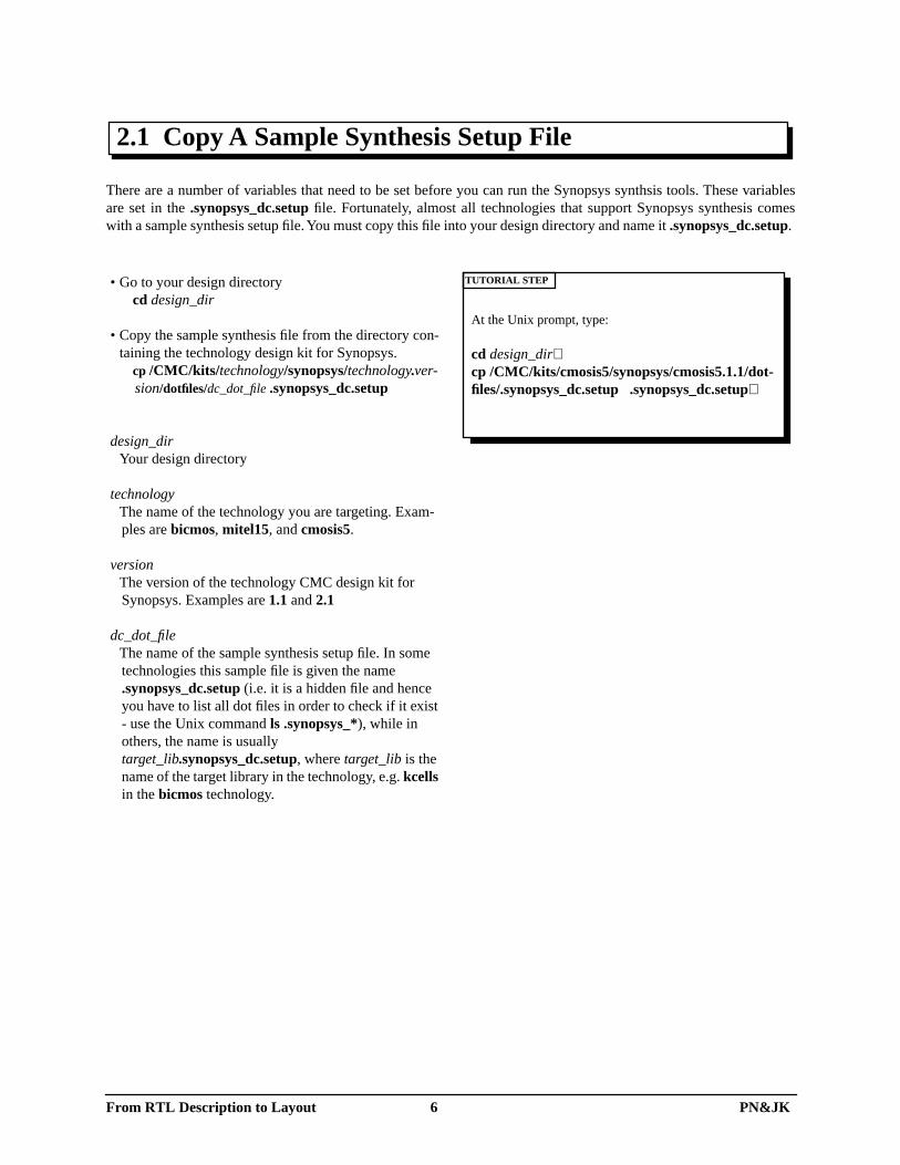
There are a number of variables that need to be set before you can run the Synopsys synthsis tools. These variablesare set in the .synopsys_dc.setup file. Fortunately, almost all technologies that support Synopsys synthesis comeswith a sample synthesis setup file. You must copy this file into your design directory and name it .synopsys_dc.setup.
2.1 Copy A Sample Synthesis Setup File
At the Unix prompt, type:
cd design_dir↵cp /CMC/kits/cmosis5/synopsys/cmosis5.1.1/dot-files/.synopsys_dc.setup .synopsys_dc.setup↵
• Go to your design directorycd design_dir
• Copy the sample synthesis file from the directory con-taining the technology design kit for Synopsys.
cp /CMC/kits/technology/synopsys/technology.ver-sion/dotfiles/dc_dot_file .synopsys_dc.setup
design_dirYour design directory
technologyThe name of the technology you are targeting. Exam-ples are bicmos, mitel15, and cmosis5.
versionThe version of the technology CMC design kit for Synopsys. Examples are 1.1 and 2.1
dc_dot_fileThe name of the sample synthesis setup file. In some technologies this sample file is given the name .synopsys_dc.setup (i.e. it is a hidden file and hence you have to list all dot files in order to check if it exist - use the Unix command ls .synopsys_*), while in others, the name is usually target_lib.synopsys_dc.setup, where target_lib is the name of the target library in the technology, e.g. kcells in the bicmos technology.
TUTORIAL STEP
From RTL Description to Layout 6 PN&JK
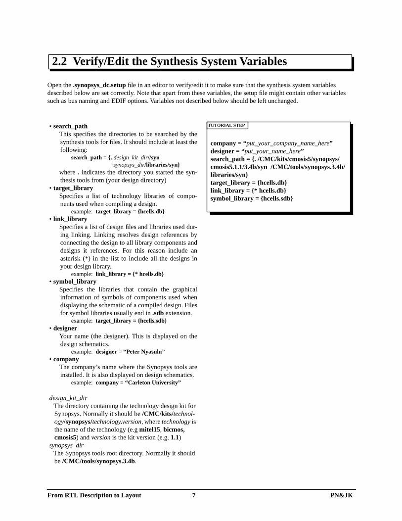
Open the .synopsys_dc.setup file in an editor to verify/edit it to make sure that the synthesis system variables described below are set correctly. Note that apart from these variables, the setup file might contain other variables such as bus naming and EDIF options. Variables not described below should be left unchanged.
2.2 Verify/Edit the Synthesis System Variables
company = “put_your_company_name_here”designer = “put_your_name_here”search_path = {. /CMC/kits/cmosis5/synopsys/cmosis5.1.1/3.4b/syn /CMC/tools/synopsys.3.4b/libraries/syn}target_library = {hcells.db}link_library = {* hcells.db}symbol_library = {hcells.sdb}
• search_pathThis specifies the directories to be searched by thesynthesis tools for files. It should include at least thefollowing:
search_path = {. design_kit_dir//synsynopsys_dir/libraries/syn}
where . indicates the directory you started the syn-thesis tools from (your design directory)
• target_librarySpecifies a list of technology libraries of compo-nents used when compiling a design.
example: target_library = {hcells.db}• link_library
Specifies a list of design files and libraries used dur-ing linking. Linking resolves design references byconnecting the design to all library components anddesigns it references. For this reason include anasterisk (*) in the list to include all the designs inyour design library.
example: link_library = {* hcells.db}• symbol_library
Specifies the libraries that contain the graphicalinformation of symbols of components used whendisplaying the schematic of a compiled design. Filesfor symbol libraries usually end in .sdb extension.
example: target_library = {hcells.sdb}• designer
Your name (the designer). This is displayed on thedesign schematics.
example: designer = “Peter Nyasulu”• company
The company’s name where the Synopsys tools areinstalled. It is also displayed on design schematics.
example: company = “Carleton University”
design_kit_dirThe directory containing the technology design kit for Synopsys. Normally it should be /CMC/kits/technol-ogy/synopsys/technology.version, where technology is the name of the technology (e.g mitel15, bicmos, cmosis5) and version is the kit version (e.g. 1.1)
synopsys_dirThe Synopsys tools root directory. Normally it should be /CMC/tools/synopsys.3.4b.
TUTORIAL STEP
From RTL Description to Layout 7 PN&JK

Most of the variables required to simulate a design using the Synopsys VHDL System Simulator (VSS) are already setup correctly in the Synopsys generic VSS setup file (.synopsys_vss.setup). However, there are still a few variables that need to be customized for your design simulation. Firstly, for gate-level simulation, you need to specify the path to the Full Time Gate-level Simulation (FTGS) libraries of your target technology. FTGS libraries contain both the gate functionality as well as gate delays. You may also optionally specify the time step of the simulation.
2.3 Setup the Synopsys VSS Simulation (VHDL Only)
hcells: /CMC/kits/cmosis5/synopsys/cmosis5.1.1//3.4b/sim/hcellsTIME_BASE = NSTIME_RES_FACTOR = 0.1EDITCMD = emacs
• Go to your design directorycd design_dir
• Using your favorite editor, open/create the file .synopsys_vss.setup. For example, if you are using emacs editor, type the following at the Unix prompt:
emacs .synopsys_vss.setup &
• In the file, specify the following variables:FTGS LibraryThis defines the names of the libraries to be used in the RTL file for gate-level simulation, as well as the path to the actual FTGS libraries (the defined library name doesn’t have to be the same as the actual name of the library). You must define this for each of the target library used in your design (libraries specified in the target_library variable in .synopsys_dc.setup file).Syntax:
gate_library: /CMC/kits/technology/synopsys/technology.version/sim/target_library_name
Example (when using the cmosis5 technology):hcells: /CMC/kits/cmosis5/synopsys/cmosis5.1.1//3.4b/sim/hcells
Simulation Time Base/ResolutionThe units and resolution of the simulation times. For example, to set simulation units to nanoseconds, and the resolution to 100 picoseconds, add the following lines in the setup file:
TIME BASE = NSTIME_RES_FACTOR = 0.1
EditorEditor that synopsys invokes when you execute any of the Synopsys environment edit file commands. The default editor is set to vi. For example, to set the editor to Emacs, include the following line in the setup file (assuming emacs is the command that is used to invoke the Emacs editor):
EDITCMD = emacs
TUTORIAL STEP
From RTL Description to Layout 8 PN&JK

3
In this step you verify the functionality of the Verilog behavioral model by simulating it using Cadence Verilog-XL Simulator. You can print the results of the simulation (in text format) using the in-built Verilog system tasks, or you can view the signals waveforms using Cadence Cwaves waveform viewer.
Simulate the Verilog RTL Model❒ Verify the Functionality of the RTL Model ❒
always @(posedge clk)begin c = a & b;end o
b
clk
From RTL Description to Layout 9 PN&JK

While it is possible to simulate a design as a stand-alone, it is advisable to simulate using a test bench. Simulating adesign using a test bench simplifies the task of specifying the simulation stimuli (since these are described in the samestyle and language as the design itself), and, more important, you can then use the very same test bench to simulatethe gate-level model (Section 6). For more information on how to write a test bench, see the example in the manualIntroduction to Verilog.To use the Cadence Cwaves waveform viewer, you must include the following Cadence-specific Simulation HistoryManager (SHM) tasks in the test bench (This is again illustrated in the test bench example in the Introduction to Ver-ilog manual):
3.1 Setup the Design Test Bench for Cadence Cwaves
In the test bench, include the following lines:
initial begin$shm_open (“shm_waves”)$shm_probe (RST, CLK, ACI, ACO)
end
initial begin$shm_open (database_directory)$shm_probe (var1, var2, ..., varn)
end
where,
database_directoryThe name of the directory where the waveforms data should be stored. Enclose the name in double quota-tion marks.
var1, var2, ..., varnThe list of Verilog variables whose waveforms should be evaluated and stored. You can then later choose which of these waveforms you display in the wave-form viewer. Note that any variable that is omitted from the probe list cannot be viewed in cwaves with-out having to re-run the whole simulation.
TUTORIAL STEP
From RTL Description to Layout 10 PN&JK

Run the Verilog-XL simulator by specifying both the test bench and the design verilog files. This will compile theVerilog source files, and if there are no errors, view the waveforms by running cwaves. While it is possible to simulatea design as a stand-alone, it is advisable to simulate using a test bench. Simulating a design using a test bench simpli-fies the task of specifying the simulation stimuli (since these are described in the same style and language as thedesign itself), and, more important, you can then use the very same test bench to simulate the gate-level model (Sec-tion 6).
3.2 Run the Simulator and Open the Waveform Viewer
At the Unix prompt, type:
verilog test_tb.v test.v↵cwaves &↵
To start the Cadence-XL simulator, at the Unix prompt, type:
verilog design_tb.v design.v
where,
design_tb.vThe name of the test bench Verilog source file.
design.vThe name of the design Verilog source file.
To start the Cadence Cwaves waveform viewer, at the Unix prompt, type:
cwaves &
TUTORIAL STEP
From RTL Description to Layout 11 PN&JK

Load the data for the waveforms into the Cadence Cwaves waveform viewer. This is done by specifying the directoryyou used in the $shm_open task in your test bench as the file name.
3.3 Load Data for the Waveforms
shm_dirThe name of the directory that was specified in the$shm_open task in the test bench. Note that thisdirectory name is typed in the File Name field, andnot in the File Path field. The default in the File Pathfield is a dot (.), which means the directory whereyou started cwaves from. If this is not the directorywhere the shm_dir is, you must specify the full pathof the directory in this field. The default for theServer Host Name, which is usually localhost,should suffice.
shm_waves
Errors, Warnings, & Reports✰ Cadence Cwaves
File Edit View Options Help
Load Data...Plot...Save Setup...
Close DataQuit
Restore Setup...
File Path:
Cancel
File Name:
OK
Server Host Name:
HelpApply
1. Type in shm_dir
2. Click
❒
From RTL Description to Layout 12 PN&JK

Select the signals you want to display and display them in the waveform viewer. Normally, the shm_dir contains thewaveforms of so many signals, but you might only want to display a few of these at a time. In this step, you can add,delete, or group waveforms into the waveform viewer.
3.4 Select and Display Signals
design_tbThe module name of the test bench. Select it by left-clicking once on it. Once the test bench module nameis selected, the subscope up/down buttons, which youare supposed to click in step 2, will be activated.
var1, var2, ...The variables whose waveforms are to be displayed.Repeat steps 3 and 4 for each of the variable you wantto display. Alternatively, you may select all the sig-nals at once in step 3 by clicking on the first variable,then hold down the shift button, and click on the last.
test_tb
RST, CLK, ACI, ACO
Errors, Warnings, & Reports✰ Cadence Cwaves
File Edit View Options Help
Browser/Display Tool...Add Signal By Name...Cut
PasteDelete
Copy
Strips
MarkersViewports
Signals
CommentsLogic OverlayDisplay Values...
Cancel Help
Delete Group
Add Selections
New...Display
Mode: Display
Hierarchical Signal Browser Grouped Waveforms
Simulation Data Display
Current Scope
▼▲ ▼ Subscopes
design_tb
Signals
var1var2
varn
Group: group0
Delete Signals
Strips1. Selectdesign_tb
3. Selectvarn
2. Click
❒4. Click 5. Click
From RTL Description to Layout 13 PN&JK

4
This step will convert the RTL model of your design into a netlist (and schematic) using the cells in the target technol-ogy library. The design is also optimized for timing and area. Synopsys power optimizations are only possible with ECL designs and hence are not covered in this manual.
Synthesize the RTL Model❒ From RTL to Schematic/Netlist ❒
always @(posedge clk)begin c = a & b;end
qdba c
clk
From RTL Description to Layout 14 PN&JK

Synopsys Design Analyzer provides a graphical (menu-driven and command-line) interface to the Synopsys tools youwill be using during synthesis (VHDL Compiler, HDL Compiler, Design Compiler, Test Compiler, Design Time).
4.1 Start the Synopsys Design Analyzer
• To start the Design Analyzer, type the following at theUnix prompt (The & starts the Design Analyzer inbackground so that you can use the Unix window forother commands):
design_analyzer &↵
• Optionally, you can use the Design Compiler (dc) shelland run the synthesis using dc shell commands only.Since the dc shell is a text-based window, you will notbe able to see the schematic. It is therefore not advis-able to use the dc shell unless you are very experi-enced with it.To start the dc shell, type the following at the Unixprompt:
dc_shell↵
Errors, Warnings, & Reports
From RTL Description to Layout 15 PN&JK
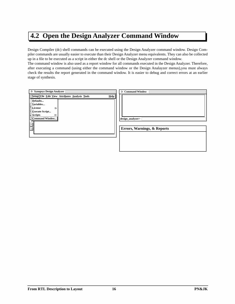
Design Compiler (dc) shell commands can be executed using the Design Analyzer command window. Design Com-piler commands are usually easier to execute than their Design Analyzer menu equivalents. They can also be collectedup in a file to be executed as a script in either the dc shell or the Design Analyzer command window.The command window is also used as a report window for all commands executed in the Design Analyzer. Therefore,after executing a command (using either the command window or the Design Analayzer menus),you must alwayscheck the results the report generated in the command window. It is easier to debug and correct errors at an earlierstage of synthesis.
4.2 Open the Design Analyzer Command Window
✰ Synopsys Design Analyzer
➩
➩
T
✰ Command Window
design_analyzer>
Errors, Warnings, & Reports
Defaults...Variables...License Execute Script...Scripts Command Window...
∆
∆
File Edit View Attributes Analysis Tools Help Setup
From RTL Description to Layout 16 PN&JK

Analyzing the RTL model checks the syntax of the VHDL/Verilog model, checks if VHDL/Verilog constructs notsupported for synthesis are used in the model, and converts the RTL into the intermediate format and stores it into thespecified or default library. Design (target, link, symbol and synthetic) libraries are also loaded at this stage.NOTE: While simulation-only constructs are treated as errors when analyzing the RTL model in the Design Analyzer,they are not when analyzed external to the Design Compiler/Analyzer (using gvan, vhdlan or Verilog XL), andhence can be used in simulation models and test benches.
4.3 Analyze the RTL Model
• Error: File ‘hdl_file’ could not be found in thesearch path ...- make sure the search path includes the directory
where the source files are. To include the directorywhere you start Design Analyzer from, include adot (‘.’) as one of the components of the searchpath.
- Unlike other stand-alone VHDL/Verilog compilers,you must specify the extension of the file (if the filehas an extension) even when a file has a standardVHDL/Verilog extension of .vhd, .vhdl or .v
• Error: Could not read the following target | link |symbol | synthentic library: ...- Check that the library you have specified in the
.synopsys_dc_setup file or using the Setup ⇒Defaults... is existent and readable and has its pathincluded in the search path.
• Error: Depending on 2 edges of same variable‘clock_pin’ not supported ...- You cannot use both the positive and negative
edges of the same clock variable in the same pro-cess or always block.
✰ Synopsys Design Analyzer
➩
➩
T
✰ Command Window
• analyze -format format hdl_file(s)↵
design_analyzer>
hdl_file(s)A list of VHDL or Verilog files. Note that Designanalyzer does not automatically append the standardVHDL/Veriolg extensions (.vhd, .vhdl, .v), andtherefore the file must be specified with its extensionif it has one.
libraryThe library where the analyzed files should be put.Normally, select the WORK or DEFAULT library,which is usually mapped to the directory where yourdesign source files are.
formatThe format of the HDL file. It is either verilog orVHDL.
clock_pinA variable used as a clock in the VHDL or Verilogdesign.
test.v(test.vhd)
WORK
CLK
Errors, Warnings, & Reports
File Name(s):Directory: /home/...
Create New Libraryif it Doesn’t Exist
File Format:
../(Move up one directory)hdl_file1.vhdl_file2.vhdl_file3.vhdhdl_file4.vhd
Verilog
Library:
DEFAULTWORK
OK Cancel
1. Selecthdl_file
2. Selectformat
3. Selectlibrary
4. Click
File Edit View Attributes Analysis Tools Help Setup
Read...Analyze...Elaborate...
SaveSave As... Save Info ∆
Plot... Quit
Import ∆
❒
From RTL Description to Layout 17 PN&JK

Elaborating builds the design from the intermediate format of a Verilog or VHDL model. The RTL model is convertedinto generic gates and logic blocks. Again, constructs not supported for synthesis (such as using both clock edges in aprocess or always block) are reported. The elaborate process also reports the memory elements (flip-flops and latches)and tristate-buffers implied in your design.
4.4 Elaborate the Design
• Error: Clock variable ‘clock_pin’ is being used asdata in ...- clock_pin, used as a clock with the statements
clock_pin’event and clock_pin = ‘1’ (= ‘0’) orposedge (negedge) clock_pin, cannot be used inthe right-hand side of an assignment statement inthe same process or always block. Use a separateprocess or always block to make this assignment.
• Error: This use of clock edge specification not sup-ported in ...- You cannot use both the positive and negative clock
edges of the same clock variable in the same pro-cess or always block.
- In VHDL, you cannot use more than oneclock_pin’event and clock_pin = ‘1’ (= ‘0’) clockstatements in one process. If possible, make allassignments in one clock statement or use morethan one process.
• Info: Inferred memory devices in process ...• Info: Inferred THREE-STATE control devices in
process ...- Always check this information about inferred
devices to make sure that your RTL description doesnot imply unnecessary flip-flops (due to variableassignments in clock_pin’event and clock_pin =‘1’ (= ‘0’) statements or always blocks withposedge (negedge) clock_pin statements), latches(due to variables not assigned to in all conditions ofif and case statements - to aviod latches, also makethe variable assignment in the else or defaultclauses of these statements), and tristate buffers.
✰ Synopsys Design Analyzer
➩
➩
T
✰ Command Window
• elaborate module↵• (elaborate entity↵)
design_analyzer>
entityThe entity name of the VHDL model. If the designcontains more than one entity, elaborate each entityseparately.
archThe architecture of the VDHL entity.
moduleThe module name of the Verilog model. If the designcontains more than one module, elaborate each mod-ule separately.
libraryThe library where the files were analyzed into. Nor-mally, select the WORK or DEFAULT library,which is usually mapped to the directory where yourdesign source files are.
clock_pinA variable used as a clock in the VHDL or Verilogmodel.
test
behav
test
WORK
CLK
Errors, Warnings, & Reports
Library:
Re-Analyze Out-Of-Date Libraries
module1(verilog)module2(verilog)entity1(arch)antity2(arch)
Parameters:
DW01DW02WORK
OK Cancel
Design:
1. Selectlibrary
2. Selectmodule(verilog)or entity(arch)
3. Turn ON
4. Click
File Edit View Attributes Analysis Tools Help Setup
Read...Analyze...Elaborate...
SaveSave As... Save Info ∆
Plot... Quit
Import ∆
❒
From RTL Description to Layout 18 PN&JK

Design and timing constraints must be set prior to compiling (mapping) the design. Constraints for clocks include theperiod (in units specified in the technology file - usually ns), skew type (either ideal clock network or that in whichthe clock delays due to the propagation delay through the clock network), whether hold time violations should be cor-rected (fixed) by inserting delays, etc. It is necessary to specify the clock period if you want to estimate the speed ofthe design (setup and hold violations) using the static timing analyzer (Design Time) after you have compiled thedesign.
4.5 Specify Clock Constraints
✰ Synopsys Design Analyzer
➩
➩
T
✰ Command Window
• create_clock -period period cck_pin↵• fix_hold clk_pin↵ • set_clock_skew -skew_type clk_pin↵
design_analyzer>
clk_pin Pin or port on which clock constraints are to be set.
periodThe period of the clock. Only the number should bespecified - the units (usually ns) are specified in thetechnology file.
skew_typeSpecifies the type of clock network. It is either ideal(an ideal clock network with no skew) or propagated(the clock skew depending on the propagation delaysthrough the network). The default is ideal.
CLK
20
propagated
Errors, Warnings, & Reports
Clock Name:
Dont Touch Network
0.0
Skew...
Period:
Cancel
Clock Port:
Fix Hold
Apply
25.0 50.0
Edge:
Clock Name:
Rise:
Cancel
Clock Delay Type
Apply
Fall:
Same Rise and Fall
Ideal
Propagated
Min:
Uncertainity
Max:
Same Min and Max
3. Turn ON
5. Click
4. Click
6. Swith ONskew_type
7. Click
8. Click 9. Click
File Edit View Attributes Analysis Tools Help Setup
❒
1. Selectclk_pin
2. Typeperiod
CLKI1I2
O1O2
Specify...Skew...
ClocksOperating EnvironmentOptimization ConstraintsOptimization Directives
∆
∆
∆
∆
From RTL Description to Layout 19 PN&JK

Synopsys Test Compiler can automatically insert boundary scan and/or scan test circuitry into your design. This man-ual covers scan test design only. The two scan test methodologies are full scan test and partial scan test. In full scantest, all sequential elements in the design are replaced by their scannable equivalents, where as in partial scan test, aconstraint-driven scan selection algorithm is used to select optimal cells to scan. Partial scan therefore has less perfor-mance and area costs than full scan, but has a lower fault coverage than the later. There are several styles of scan-testimplementation. Multiplexed flip-flop scan test design is the most commonly supported scan test style. In this imple-mentation, the input to a flip flop is multiplexed between the normal circuit data and the scan test. The other scanstyles are described briefly in Appendix A.1.NOTE: For menu-driven execution, test methodology is set later when the test circuitry is just about to be inserted.
4.6 Set Test Methodology and Scan Test Style
✰ Synopsys Design Analyzer
➩
➩
T
✰ Command Window
• set_test_methodology test_methodology↵• set_scan_style scan_style↵
design_analyzer>
test_methodologyThe test methodolgy to be used. It is either full_scanor partial_scan. The default is full_scan.
scan_styleDefines the scan-test implementation. It is eithermultiplexed_flip_flop, lssd, aux_clock_lssd,clocked_scan, combinational or none. See Appen-dix A.1 for details.
full_scan
multiplexed_flip_flop
Errors, Warnings, & Reports
Design...Input Port...Output Port...Cell...Pin... Net...Timing Paths...
1. Selectscan_style
2. Click
3. Click
File Edit View Attributes Analysis Tools Help Setup
ClocksOperating EnvironmentOptimization ConstraintsOptimization Directives
∆
∆
∆
∆
Design Name:
Flatten Effort:
CancelApply
Structured Logic
Low
Boundary Optimization
Port is Pad:
Ungroup
Disable Wired Logic (E
Single Output
Flatten Minimize: Flatten Phase:
Don’t ApplyMedium Multiple Output Apply StrategyHigh None
Flatten Logic
Don’t Touch
Test Scan Style: None
Design Pad Attributes...
Apply Timing Driven Structuring
Apply Boolean Optimization
Sequential Elements: Latch...Flip Flop...
❒
For S
can T
est O
nly
From RTL Description to Layout 20 PN&JK

Apart from clock and test constraints, there are a number of other attributes that you might need to set before compil-ing your design. The Synopsys Command Reference Manual lists all the available attributes. However, in most cases,the default settings of most attributes suffice. A few common design constraints that need to be set include:• Maximum Fanout: sets the maximum fanout for driving pins (default value can be set for the library)• Maximum Transition Time: The maximum time required for driving pins to change logic values.• Speed vs. Area: whether timing is critical in the design when compared to area.NOTE: for command-line execution, the timing-is-critical attribute is set later with the compile command.
4.7 Set Other Design Constraints
✰ Synopsys Design Analyzer
➩
➩
T
✰ Command Window
• set_max_fanout max_fanout design↵• set_max_transition max_trans design↵
design_analyzer>
max_fanoutThe value of the maximum fanout.
max_transThe maximum transition time. Only the numbershould be specified, but its units must be consistentwith those specified in the technology library (usuallyns).
designName of the design (entity name or module name)
10
2.0
test
Errors, Warnings, & Reports
Design Name:
Max Area:
CancelApply
Max Power:
Optimization Constraints:
Area Critical Timing Critical
Test Constraints:
Min Fault Coverage: 95%
Max Fanout:Max Transition:
Design Rules:
1. Typemax_fanout
4. Click 5. Click
2. Typemax_trans
3. Turn ON
❒
File Edit View Attributes Analysis Tools Help Setup
ClocksOperating EnvironmentOptimization ConstraintsOptimization Directives
∆
∆
∆
∆ Derive...
Design Constraints...Timing Constraints...
From RTL Description to Layout 21 PN&JK

This step performs logic and gate-level synthesis and optimization. The result is a netlist (and a schematic) of thedesign using the cells in the target library. During optimization, the Design Compiler tries to meet the user-specifieddesign constraints.
4.8 Compile the Design
✰ Synopsys Design Analyzer
➩
➩
T
✰ Command Window
• compile -map_effort map_effort↵
design_analyzer>
map_effortSpecifies how much effort and time should be spentby the processor on mapping. Valid settings are Low,Medium and High. High effort yields a better opti-mized circuit, but the CPU time taken to achieve thismight be too much for very large designs. The defaultmap effort is Medium.
medium
Errors, Warnings, & Reports
Design Optimization...Finite State Machines...FPGA Compiler...
Map Effort:
Cancel
Map Design
Low Medium High
Allow Boundary Optimization
More Map Options...
Map Effort:
Verify Design
Low Medium High
Execute in: Foreground Background
OK4. Click
2. Turn ONmap_effort
1. Turn ON
❒
3. Turn ON
File Edit View Attributes Analysis Tools Help Setup
Test Synthesis...
From RTL Description to Layout 22 PN&JK

This checks the current design for problems. All errors must be corrected. While most warnings can be ignored, it isnecessary to check each one of them since some warnings might actually indicate errors in the logic of the design.
4.9 Check the Design Rules
• Warning: In design ‘design’ port ‘port_name’ isnot connected to any nets.- Make sure that the port port_name is intentionally
not associated with any logic in your HDL descrip-tion. Otherwise if the port is included for futureexpansion of the design, or for component inter-face consistency, the warning may be ignored.
✰ Synopsys Design Analyzer
➩
➩
T
✰ Command Window
• check_design↵
design_analyzer>
designThe name of the design you are currently checking.
port_nameThe name of any port on your design.
test
Errors, Warnings, & Reports
OK
Check Timing
Options
Detailed Warnings
Exclude WarningsSummarize Warnings
Options
Check All LevelsCheck Current Level
Cancel3. Click
❒
2. Turn ON
1. Turn ON
File Edit View Attributes Analysis Tools Help Setup
Link Design...Check Design...Time Design Show Timing...
Highlight Show Net Load...
∆
Test Report...Report...
From RTL Description to Layout 23 PN&JK
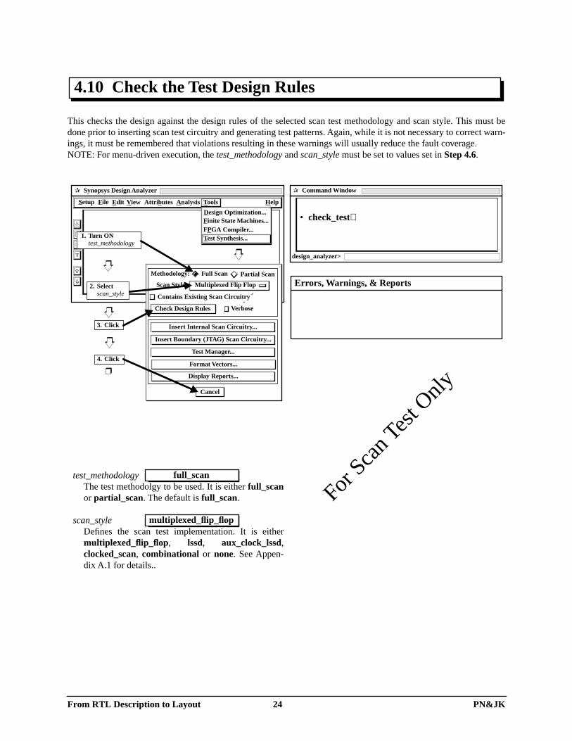
This checks the design against the design rules of the selected scan test methodology and scan style. This must bedone prior to inserting scan test circuitry and generating test patterns. Again, while it is not necessary to correct warn-ings, it must be remembered that violations resulting in these warnings will usually reduce the fault coverage.NOTE: For menu-driven execution, the test_methodology and scan_style must be set to values set in Step 4.6.
4.10 Check the Test Design Rules
✰ Synopsys Design Analyzer
➩
➩
T
✰ Command Window
• check_test↵
design_analyzer>
test_methodologyThe test methodolgy to be used. It is either full_scanor partial_scan. The default is full_scan.
scan_styleDefines the scan test implementation. It is eithermultiplexed_flip_flop, lssd, aux_clock_lssd,clocked_scan, combinational or none. See Appen-dix A.1 for details..
full_scan
multiplexed_flip_flop
Errors, Warnings, & Reports
Cancel
VerboseCheck Design Rules
Contains Existing Scan Circuitry
Methodology: Full Scan Partial Scan
Scan Style: Multiplexed Flip Flop
Insert Internal Scan Circuitry...
Insert Boundary (JTAG) Scan Circuitry...
Test Manager...
Format Vectors...
Display Reports...
4. Click
1. Turn ONtest_methodology
❒
2. Selectscan_style
3. Click
File Edit View Attributes Analysis Tools Help Setup
Design Optimization...Finite State Machines...FPGA Compiler...Test Synthesis...
For S
can T
est O
nly
From RTL Description to Layout 24 PN&JK

At this point, you can optionally estimate the test fault coverage by running automatic test pattern generation (ATPG)on the design. This is especially important if you had warnings when running check test design rules in Step 4.10. Byrunning ATPG at this point, you get an idea of the effect that the warnings (usually uncontrollable pins) have on thefault coverage. You can then decide whether to correct the warnings or not. Appendix A.1 lists some common testdesign rule violations and how they can be corrected.
4.11 Estimate Test Fault Coverage
• Warning: Design has no scan path. Generatedvectors will not be saved.- Ignore this warning. It simply reminds you that you
have run ATPG before inserting scan test circuitry.ATPG will be run again later.
✰ Synopsys Design Analyzer
➩
➩
T
✰ Command Window
• create_test_patterns↵
design_analyzer>
Errors, Warnings, & Reports
Cancel
VerboseCheck Design Rules
Contains Existing Scan Circuitry
Methodology: Full Scan Partial Scan
Scan Style: Multiplexed Flip Flop
Insert Internal Scan Circuitry...
Insert Boundary (JTAG) Scan Circuitry...
Test Manager...
Format Vectors...
Display Reports...
5. Click
❒
1. Click
4. Click
File Edit View Attributes Analysis Tools Help Setup
Design Optimization...Finite State Machines...FPGA Compiler...Test Synthesis...
Cancel
Create Test Patterns...
Fault Simulate...
Analyze Fault Coverage...
Restore/Delete Test Program...
Multi-pass Test Generation ?Yes No
Cancel
Compact Patterns
Additional Options...
Execute in:
Foreground Background
OK
Test Pattern Generation Options:Use Initial Pattern File:
Initial File:
Output Pattern File:
design.vdb
Contention CheckFloat Check
Efoort: Low (Backward)
2. Click
3. Click For S
can T
est O
nly
From RTL Description to Layout 25 PN&JK

If you want to see the effect that scan insertion has on the area and performance of the design, you must analyze thedesign for area and timing before and after scan test insertion. You can then decide whether to incrementally optimizethe design to try and meet the performance and area of the design without scan, or to change the test strategy alltogether.
4.12 Perform Area and Timing Analysis
• Report: In the contraints report, note the (MET) and(VIOLATED) against each of the design constraintsset earlier.- This shows that the design constraint has either
been met or violated by the indicated value.
• Report: In the timing report, note the slack (MET)at the end of the report.
- This indicates the time that the longest path in thedesign settles before the clock changes. A negativevalue indicates a violation. Increase the clockperiod or reoptimize the design if there is a slackviolation.
✰ Synopsys Design Analyzer
➩
➩
T
✰ Command Window
• report_area↵• report_constraints↵• report_timing↵
design_analyzer>
Errors, Warnings, & Reports
Attribute Reports
CancelApply
All Attributes Compile Options
Clear ChoicesSet Options...
Path GroupsBussing Design PortCell FSM ResourceClocks Net
Analysis Reports
Area Cross Ref. ReferenceClock Skew Hierarchy SelectedClock Tree Point Timing TimingConstraints Power Timing Requ
Send Output To: Window File
File:
5. Click
❒
3. Turn ON
2. Turn ON
1. Turn ON
4. Click
File Edit View Attributes Analysis Tools Help Setup
Link Design...Check Design...Time Design Show Timing...
Highlight Show Net Load...
∆
Test Report...Report...
From RTL Description to Layout 26 PN&JK

This step adds test circuitry to the design. Basically, all sequential cells (flip-flops and latches) are replaced by theirscannable versions and/or logic is added to multiplex between scan test serial shifting and normal circuit operation.Pins for scan test enable (test_se) and scan test shift input (test_si) are also added to the design. By default, Test Compiler also adds logic to disable internal three-state bus drivers to ensure that only one driverdrives the bus at a time. Since this will more likely have already been incorporated in your design (otherwise chancesare that you have an erroneous design with bus contention), you must prevent Test Compiler from adding this dis-abling logic by running test insertion with the no_disable option.
4.13 Insert Scan Test Circuitry
• Warning: Deleting current test program‘test_program_name’ because it is not consistentwith the current design.- Again, ignore this warning. It refers to the ATPG
that was run in step 6.11. Since the design haschanged, the next ATPG will use a new initial faultlist.
✰ Synopsys Design Analyzer
➩
➩
T
✰ Command Window
• insert_test -no_disable↵
design_analyzer>
test_programThe test program that was created with the last ATPGrun and is currently being deleted.
test.vdb
Errors, Warnings, & Reports
Cancel
VerboseCheck Design Rules
Contains Existing Scan Circuitry
Methodology: Full Scan Partial Scan
Scan Style: Multiplexed Flip Flop
Insert Internal Scan Circuitry...
Insert Boundary (JTAG) Scan Circuitry...
Test Manager...
Format Vectors...
Display Reports...
Insert Scan Options:
Cancel
Disable Internal Three-State Drivers
Insert Test Cells
Maximum Scan Chain Length:Number of Scan Chains:
Route Scan Path
Execute in:
Foreground Background
OK
3. Click
❒
2. Turn OFF
1. Click
4. Click
File Edit View Attributes Analysis Tools Help Setup
Design Optimization...Finite State Machines...FPGA Compiler...Test Synthesis...
For S
can T
est O
nly
From RTL Description to Layout 27 PN&JK

Now that scan circuitry has been added, it is possible that some design constraints, which were originally met, willnow be violated. Obviously, the scan circuitry has added extra area. It is therefore very important to re-run the areaand timing analysis as was done in Step 4.12. If there are timing violations, or if you simply want to further optimizethe design area and timing, you must now run an incremental compilation. Incremental compilation uses the existingcompiled gate-level design to improve the design constraints. If no improvements can be made, the design is leftunchanged. After running incremental optimization, you must once again run area and timing analysis (Step 4.12) to check if thedesign now meets all the design constraints. If the design does not meet timing constraints even after several optimi-zations and/or redesign, you may wish to consider increasing the clock period and/or relaxing some of the timing con-straints.
4.14 Optimize the Scan Design
✰ Synopsys Design Analyzer
➩
➩
T
✰ Command Window
• compile -incremental_mapping↵
design_analyzer>
Errors, Warnings, & Reports
Map Effort:
Cancel
Map Design
Low Medium High
Allow Boundary Optimization
More Map Options...
Map Effort:
Verify Design
Low Medium High
Execute in: Foreground Background
OK
Incremental Mapping
OK
Prioritize Min PathsMap in Place
❒
3. Click
4. Click
1. Click
2. Turn ON
File Edit View Attributes Analysis Tools Help Setup
Design Optimization...Finite State Machines...FPGA Compiler...Test Synthesis...
Step 6.12 (Area and Timing Analysis) Step 6.12 (Area and Timing Analysis)
Step 6.12 (Area and Timing Analysis)
Step 6.12 (Area and Timing Analysis)
For S
can T
est O
nly
From RTL Description to Layout 28 PN&JK

Again, check the test design rules as outlined in Step 4.10. If there are no violations, you now need to know whichports of the design are used for scan test. The input ports test_se and test_si have been added by the Test Compilerspecifically for scan test. However, Test Compiler multiplexes one of the design output ports to be used as a scan out-put port during scan test. It is necessary to find out which port is used as the scan output in order to define it correctlywhen you set up the chip pins for scan test (Step 4.23). Apart from the scan ports, you can also optionally report theactual scan chain (cells in the scan path).
4.15 Check Test Design Rules & Report Scan Path
✰ Synopsys Design Analyzer
➩
➩
T
✰ Command Window
• check_test↵• report_test -scan_path -port↵
design_analyzer>
Errors, Warnings, & Reports
Cancel
VerboseCheck Design Rules
Contains Existing Scan Circuitry
Methodology: Full Scan Partial Scan
Scan Style: Multiplexed Flip Flop
Insert Internal Scan Circuitry...
Insert Boundary (JTAG) Scan Circuitry...
Test Manager...
Format Vectors...
Display Reports...
2. Click
1. Turn ON
CancelApply
Assertions JTAG
ATPG Conflicts MethodologyConstraints Ports
Coverage Scan Path
Send Output To: Window File
File:
Don’t Fault
Faults Fault Options: Untested
3. Turn ON
4. Turn ON
5. Click
6. Click
❒
7. Click
File Edit View Attributes Analysis Tools Help Setup
Design Optimization...Finite State Machines...FPGA Compiler...Test Synthesis...
Step 4.10 (Check Test Design Rules)
For S
can T
est O
nly
From RTL Description to Layout 29 PN&JK

You may now save the design in the Synopsys internal database (DB) format. This is important if you wish to stop atthis stage and continue the design process later. The saved db file will allow you to read in the synthesized gate-leveldesign without having to compile it again from the RTL model.The save command outlined here will save all the designs in the hierarchy in a file named design.db, where design isthe name of the top-level entity (VHDL) or top-level module (Verilog). To save the design using a different name or adifferent format, or to save the top-level without the other designs in the hierarchy, use the Save As... command asoutlined in Step 4.25. If you decide to use the Save As... command for this step, make sure that you select the DB(Synopsys internal database) format and save all the designs in the hierarchy. You may however use a different filename than the default.
4.16 Save the Core Design
✰ Synopsys Design Analyzer
➩
➩
T
✰ Command Window
• write -format db -hierarchy↵
design_analyzer>
Errors, Warnings, & Reports
File Edit View Attributes Analysis Tools Help Setup
Read...Analyze...Elaborate...
SaveSave As... Save Info ∆
Plot... Quit
Import ∆
From RTL Description to Layout 30 PN&JK

The core design just completed does not have pads. To insert pads, you must write an RTL model of the chip with aninstantiation of the core design. There are two reasons why it is advisable to use this approach. Firstly, scan insertionhas to be done on the core design, without the pads, and then routed to the pads later. Secondly, in order for SynopsysDesign Compiler to automatically insert the pads, the RTL code must imply the type of pads available in the technol-ogy library. While there are almost no problems with input pads (Design Compiler will automatically insert an inputpad for each input port on the top-level design), Design Compiler will issue an error (Error: No matching padfound for port...) if the RTL code, say, implies a standard output pad but the library only contains pads with outputenable (three-state) control pin and vice versa. Therefore, this step has a very high potential of being technology-dependent. However, it must be noted that in most technologies, output pads fall into two categories: those with out-put enable pins, and those without. Therefore, you can write RTL code to imply one type of pad and if Design Com-piler issues an error, change the code to imply the other type. The most common type of output pad is one with outputenable pin (These are the pads available in Mitel 1.5 µm and Nortel 0.8 µm BiCMOS technologies). Therefore, firstwrite your RTL code to imply this pad type.
4.17 Generate the Chip RTL Model (Verilog)
module testchip (test_si, test_se, RST, CLK, ACI, ACO);input test_si, test_se;input RST, CLK;input [2:0] ACI;output [2:0] ACO;
test c_core (.test_si(test_si), .test_se(test_se),.RST(RST), .CLK(CLK),.ACI(ACI), .ACO(ACO));
endmodule;
• For illustration purposes, assume that the core RTLmodel has the ports input I; output O1; output [3:0]O2;
• Suggested names for chip Verilog file and module aredesignchip.v and designchip, respectively.
• In both the chip module and the core componentinstantiation, include all the ports in the core Verilogmodel, and also add the following two ports :
input test_si, test_se;
• For pads with output enables,- Declare a variable to control the output enable:
reg pads_oe;- Declare an internal variable for each core output port:
reg O1_i;reg [3:0] O2_i;
- Write an always block to control the output pads:always @(pads_oe or O1_i or O2_i) begin
if (pads_oe == 1’b1) begin O1 = O1_i; O2 = O2_i;
endelse begin
O1 = 1‘bZ; O2 <=4’bZ;endpads_oe = 1’b1;
end
• For pads with output enable, instatiate the core as:design c_core port map (.test_si(test_si), .test_se(test_se), .I(I), .O1(O1_i), .O2(O2_i))
• For pads without output enable, instatiate the core as:design c_core port map (.test_si(test_si),.test_se(test_se), .I(I), .O1(O1), .O2(O2))
designthe core design module name
test
TUTORIAL STEP
From RTL Description to Layout 31 PN&JK

The core design just completed does not have pads. To insert pads, you must write an RTL model of the chip with aninstantiation of the core design. There are two reasons why it is advisable to use this approach. Firstly, scan insertionhas to be done on the core design, without the pads, and then routed to the pads later. Secondly, in order for SynopsysDesign Compiler to automatically insert the pads, the RTL code must imply the type of pads available in the technol-ogy library. While there are almost no problems with input pads (Design Compiler will automatically insert an inputpad for each input port on the top-level design), Design Compiler will issue an error (Error: No matching padfound for port...) if the RTL code, say, implies a standard output pad but the library only contains pads with outputenable (three-state) control pin and vice versa. Therefore, this step has a very high potential of being technology-dependent. However, it must be noted that in most technologies, output pads fall into two categories: those with out-put enable pins, and those without. Therefore, you can write RTL code to imply one type of pad and if Design Com-piler issues an error, change the code to imply the other type. The most common type of output pad is one with outputenable pin (These are the pads available in the Mitel 1.5 µm and Nortel 0.8 µm BiCMOS technologies). Therefore,first write your RTL code to imply this type of pad.
4.18 Generate the Chip RTL Model (VHDL)
entity testchip isport ( test_si, test_se: in std_logic;
RST, CLK: in std_logic;ACI: in std_logic_vector (2 downto 0);ACO: out std_logic_vector (2 downto 0));
end testchip;
architecture behav of testchip is
component testport ( test_si, test_se: in std_logic;
RST, CLK: in std_logic;ACI: in std_logic_vector (2 downto 0);ACO: out std_logic_vector (2 downto 0));
end component;
begin
c_core: test port map (test_si=>test_si,test_se=>test_se, RST=>RST, CLK=>CLK,ACI=>ACI, ACO=>ACO);
end behav;
• For illustration purposes, assume that the core RTLmodel has the ports I: in std_logic; O1: out std_logic;O2: out std_logic_vector(3 downto 0);
• Suggested names for chip VHDL file and entity aredesignchip.vhd and designchip, respectively.
• In both the chip entity and the core component declara-tion, include all the ports in the core RTL model, andalso add the following two ports :
test_si: in std_logic;test_se: in std_logic;
• For pads with output enables,- Declare a signal to control the output enable:
signal pads_oe : std_logic;- Declare an internal signal for each core output port:
signal O1_i: std_logic;signal O2_i: std_logic_vector(3 downto 0);
- Write a process to control the output pads:PadsProcess: process (pads_oe, O1_i, O2_i) begin
if (pads_oe = ‘1’) then O1 <= O1_i; O2 <= O2_i;
else O1 <= ‘Z’; O2 <= “ZZZZ”;
end if;end process PadsProcess;pads_oe <= ‘1’;
• For pads with output enable, instatiate the core as:c_core: design port map (test_si=>test_si, test_se=>test_se, I=>I, O1=>O1_i, O2=>O2_i)
• For pads without output enable, instatiate the core as:c_core: design port map (test_si=>test_si,test_se=>test_se, I=>I, O1=>O1, O2=>O2)
designthe core design entity name
test
TUTORIAL STEP
From RTL Description to Layout 32 PN&JK

Analyze the chip RTL model (Step 4.3), and elaborate it (Step 4.4). Then set the design constraints; this mightinclude specifying the clock (Step 4.5), test constraints (Step 4.7) and other design constraints (Step 4.6). NOTE that since the core design already contains scan circuitry (and you are not adding any new scan circuitry on thechip design), you must include the -existing_scan option (or when using menus, turn ON the Contains ExistingScan Circuitry button) when you specify the scan methodology.
4.19 Analyze, Elaborate and Constrain the Chip
1hdl_fileFor the Analyze command hdl_file(s), select/specifythe chip HDL file you created in Step 4.17/Step 4.18.Do not specify the core design HDL file. All otherinformation is the same as for the previous (coredesign) Analyze command execution.
2entity/moduleFor the Elaborate command entity or module, selectthe select/specify the entity or module name of the-chip HDL model created in Step 4.17/Step 4.18. Donot specify the core deisgn entity or module. If youuse a different architecture name for the chip design,remember to specify it, otherwise all the other infor-mation is the same as that when you executed atheElaborate command for the core design.
3For command-line execution, when you run theset_test_methodology command, remember to run itwih the option -exisiting_scan to tell Design/Test Com-piler that the design already contains scan circuitry. Forexample, to set test methodolody to full scan, run thecommand as follows:
set_test_methodology full_scan -existing_scan↵
Other constraints should be set as for the core design.
test_chip.v (test_chip.vhd)
test_chip
Step 4.3 (Analyze the chip hdl_file)1
Step 4.4 (Elaborate the chip entity or module)2
Step 4.5 - Step 4.7 (Constrain the chip design)3
Errors, Warnings, & Reports
From RTL Description to Layout 33 PN&JK

Since the core design is already optimized, you must set a dont_touch attribute on the core instance in order to preventDesign Compiler from trying to re-optimize the design. All logic necessary for pad insertion is thus external to thecore. This makes debugging easier, and also ensures that most of the analysis done earlier on the core are not invali-dated with insertion of extra logic into the core design.
4.20 Set Dont Touch Attribute on the Core
✰ Synopsys Design Analyzer
➩
➩
T
✰ Command Window
• set_dont_touch instance_name↵
design_analyzer>
instance_nameThe name of the instance of the core design in thechip. Note that this is not the design (entity or mod-ule) name of the core, but rather the name of theinstance or component when it is instantiated in thechip design.
c_core
Errors, Warnings, & Reports
Design...Input Port...Output Port...Cell...Pin... Net...Timing Paths...
File Edit View Attributes Analysis Tools Help Setup
ClocksOperating EnvironmentOptimization ConstraintsOptimization Directives
∆
∆
∆
∆
Cell Name:
CancelApply
Scan Replacement:
Sequential Elements:
Always
Ungroup Cell’s Hierarchy
Latch...
Compile Attributes:
Flip Flop...
Referencing:
instance_name
cell_design_name
Don’t TouchAllow Boundary Optimization
Max Time Borrow:
Never
3. Turn ON
4. Click
5. Click
CLKI1I2
O1O2
2. Select
1. Click
❒
From RTL Description to Layout 34 PN&JK

In order for a pad to be inserted on a design port, the port must be specified as a pad using the set_port_is_padattribute. Other pad attributes, such as... may also be specified before the actual pad insertion process.
4.21 Set Pad Attributes
✰ Synopsys Design Analyzer
➩
➩
T
✰ Command Window
• set_port_is_pad “*”↵
design_analyzer>
Errors, Warnings, & Reports
File Edit View Attributes Analysis Tools Help Setup
Design...Input Port...Output Port...Cell...Pin... Net...Timing Paths...
2. Click
3. Click
ClocksOperating EnvironmentOptimization ConstraintsOptimization Directives
∆
∆
∆
∆
Design Name:
Flatten Effort:
CancelApply
Structured Logic
Low
Boundary Optimization
Port is Pad:
Ungroup
Disable Wired Logic (E
Single Output
Flatten Minimize: Flatten Phase:
Don’t ApplyMedium Multiple Output Apply StrategyHigh None
Flatten Logic
Don’t Touch
Test Scan Style: None
Design Pad Attributes...
Apply Timing Driven Structuring
Apply Boolean Optimization
Sequential Elements: Latch...Flip Flop...
❒
1. Turn ON
From RTL Description to Layout 35 PN&JK

This step will physically insert pads on all the ports that have been set up for pad insertion in Step 4.21 and optimizethe design. Pads must be inserted before the design is compiled. Also since the core design has already been opti-mized, only incremental compilation (Step 4.14) is necessary.
4.22 Insert Pads & Optimize the Design
✰ Synopsys Design Analyzer
➩
➩
T
✰ Command Window
• insert_pads↵ • compile -incremental_compilation↵
design_analyzer>
Errors, Warnings, & Reports
File Edit View Attributes Analysis Tools Help Setup
DeleteInsert Pads...Select...
Group...Ungroup... Uniquify ∆
Reset...
Unselect All
Cancel
Set Pad Type
Design Pad Attributes...
Effort:
Verify Results
Low Medium High
OK
Port Pad Attributes...❒
1. Click
Step 4.14 (Incremental Compilation)
From RTL Description to Layout 36 PN&JK

To route the core design scan circuitry to the chip pads, you must specify the chip pins that are to be used as scan pins(scan enable, scan input, and scan output). The scan input pins are test_se and test_si.
4.23 Define the Chip Scan Input Pins
✰ Command Window
• set_signal_type test_scan_enable test_se↵ • set_signal_type test_scan_in test_si↵
design_analyzer>
Errors, Warnings, & Reports
✰ Synopsys Design Analyzer
➩
➩
T
File Edit View Attributes Analysis Tools Help Setup
ClocksOperating EnvironmentOptimization ConstraintsOptimization Directives
∆
∆
∆
∆
Design...Input Port...Output Port...Cell...Pin... Net...Timing Paths...
Port Name:
Maximum Fanout:
CancelApply
Maximum Transition:
Logic 0
Test Hold: None
Connected to:
selected_port
Port is Pad: Port Pad Attributes...
Logic 1
Set Opposite...Set Equal...
Signal Type: Scan Enable
4. Click
8. Click
❒
3. SelectTest Scan Enable
6. SelectTest Scan In
5. Select Pintest_si
7. Click
CLKI1I2
test_setest_si
O1O21. Click
2. Select Pintest_se
For S
can T
est O
nly
From RTL Description to Layout 37 PN&JK

As mentioned earlier, Test Compiler multiplexes one of design output pin to be used as the output pin during scanshift. This pin was reported in Step 4.15. You should now configure it as the chip scan output pin.
4.24 Define the Chip Scan Output Pin
✰ Command Window
• set_signal_type test_scan_out scan_out↵
design_analyzer>
scan_outThe design output pin that is also used (multiplexed)as a scan output pin. This pin was reported inStep 4.15 when you run the report_test command.
O
Errors, Warnings, & Reports
✰ Synopsys Design Analyzer
➩
➩
T
File Edit View Attributes Analysis Tools Help Setup
ClocksOperating EnvironmentOptimization ConstraintsOptimization Directives
∆
∆
∆
∆
Design...Input Port...Output Port...Cell...Pin... Net...Timing Paths...
3. Click
4. Click
❒
1. Select Pinscan_out
2. SelectTest Scan Out
Port Name:
CancelApply
Maximum Transition:
Unonnected
selected_port
Port is Pad: Port Pad Attributes...
Signal Type: Scan Out
CLKI1I2
test_setest_si
O1O2
For S
can T
est O
nly
From RTL Description to Layout 38 PN&JK

Pad insertion may sometimes introduce additional test design rule violations. You must therefore once again runcheck test before you save the final design. You can also, optionally, report the scan chain and scan ports to make surethat the core design scan circuitry is correctly routed to the chip pins.
4.25 Check Test, Report Scan Path & Save Design
✰ Command Window
• report_test -scan_path -port↵• write -format db -hierarchy↵
design_analyzer>
Errors, Warnings, & Reports
✰ Synopsys Design Analyzer
➩
➩
T
File Edit View Attributes Analysis Tools Help Setup
Read...Analyze...Elaborate...
SaveSave As... Save Info ∆
Plot... Quit
Import ∆
Step 4.15 (Check Test Rules & Report Scan)
From RTL Description to Layout 39 PN&JK

So far the design has been saved in the Synopsys internal database format (db). But in order to export the design tothird part tools for placement and routing, the design has to be saved in a format other than db. Also, to simulate thegate-level design (Step 5), the design must be saved in the required HDL format. The saved HDL design is simply astructural hierarchical HDL code with the lowest level consisting of the interconnections of the technology librarycomponents as they appear in the schematic. Therefore, you must now save the design twice, firstly in Verilog orVHDL format (for simulation), and then in the format required by the third party tool (e.g. EDIF to import a Nortel0.8 um BiCMOS design to Cadence, Verilog to import a Mitel 1.5 um design to Cadence, XNF to import a Xilinxdesign to the XACT tools).
4.26 Save the Design in HDL and Export Formats
✰ Synopsys Design Analyzer
➩
➩
T
File Edit View Attributes Analysis Tools Help Setup
✰ Command Window
• write -format file_format -hierarchy -output file_name↵
design_analyzer>
file_nameThe name of the file that the design has to be savedas. When saving the HDL gate-level file, make surethat you specify a different file name from the onecontaining behavioral design.
file_formatThe format in which you want the design to be saved.Valid formats are:
db Synopsys internal database formatvhdl IEEE Standard VHDLverilog Cadence Verilog HDLedif Electronic Design Interchange Formatxnf Xilinx Netlist Formatmif Mentor Interchange Format (MIF)equation Synopsys equation formatst Synopsys State Table formattegas Tegas design Language netlist Fornatlsi LSI Logic Corporation Netlist Formatpla Berkeley (Espresso) PLA format
test_g.v
verilog
Errors, Warnings, & Reports
File Name:Directory: /home/...
Save All Designsin Hierarchy
File Format:
../(Move up one directory)file1file2file3file4
DB
OK Cancel
Read...Analyze...Elaborate...
SaveSave As... Save Info ∆
Plot... Quit
Import ∆
4. Click
❒
1. Typefile_name
1. Selectfile_name
2. Selectfile_format
or
3. Turn ON
Perform this step twice: first for the HDL format (e.g. verilog), and then for the export format (e.g. edif)
From RTL Description to Layout 40 PN&JK

A few timing parameters need to be set prior to generating test vectors (ATPG) and running fault simulation(TestSim). The most common ones include the test defaut delay and strobe times, as well as the timing parameters ofthe test clock. These are briefly described below:• test_default_delay
For ATPG, this value defines the time at which values are applied to the primary inputs. Its value must be less thanboth the output strobe time and the capture clock edge value. The value set for test_default_delay is used by thecheck_test command when checking the design against the design rules of the scan test methodology. It is also usedby the write_test command when producing a test program.For TestSim, the value of test_default_delay defines the default input delay for primary inputs, and must be set to thevalue that was used when generating the vectors being input to TestSim. It must be less than the clock period.
• test_default_strobeThis defines the default time at which values are strobed at the primary outputs and bidirectional ports. Its valuemust be less than the clock period. test_default_strobe also affests both the check_test and write_test commands.
• test clock parametersThis includes the period, waveform and default period of the clock to be used during test.
4.27 Specify Test Timing Parameters
✰ Command Window
• test_default_period = default_period↵• test_default_delay = default_delay↵• test_default_strobe = default_strobe↵• create_test_clock clock_pin -period period
-waveform {rise_edge fall_edge}↵design_analyzer>
clock_pin Pin to be used as clock during test.
periodValue of the period of the test clock in ns.
default_periodValue of the default period of the test clock in ns.
default_delayValue of the default test delay in ns.
default_strobeValue of the default test strobe time in ns.
rise_edge fall_edgeRise and fall edge times of the test clock over oneperiod (typically, the first edges after time zero).
CLK
100
100
5
95
45 55
Errors, Warnings, & Reports
✰ Synopsys Design Analyzer
➩
➩
T
File Edit View Attributes Analysis Tools Help Setup
For S
can T
est O
nly
From RTL Description to Layout 41 PN&JK

In this step, Test Compiler uses the ATPG to generate a minimal set of scan test vectors to test your design for all pos-sible stack-at faults. The fault coverage achieved by these test vectors, plus the number of detected and undetected(untested) faults is also reported.
4.28 Generate Test Vectors
✰ Synopsys Design Analyzer
➩
➩
T
✰ Command Window
• create_test_patterns -compaction_effort low↵
design_analyzer>
Errors, Warnings, & Reports
Cancel
VerboseCheck Design Rules
Contains Existing Scan Circuitry
Methodology: Full Scan Partial Scan
Scan Style: Multiplexed Flip Flop
Insert Internal Scan Circuitry...
Insert Boundary (JTAG) Scan Circuitry...
Test Manager...
Format Vectors...
Display Reports...
5. Click
❒
1. Click
4. Click
File Edit View Attributes Analysis Tools Help Setup
Design Optimization...Finite State Machines...FPGA Compiler...Test Synthesis...
Cancel
Create Test Patterns...
Fault Simulate...
Analyze Fault Coverage...
Restore/Delete Test Program...
Multi-pass Test Generation ?Yes No
Cancel
Compact Patterns
Additional Options...
Execute in:
Foreground Background
OK
Test Pattern Generation Options:Use Initial Pattern File:
Initial File:
Output Pattern File:
design.vdb
Contention CheckFloat Check
Efoort: Low (Backward)
2. Click
3. Click
For S
can T
est O
nly
From RTL Description to Layout 42 PN&JK

It is important to analyze the fault coverage and obtain a detailed report especially for untested faults (you can alsoreport on faults that are redundant, oscillating, etc.). Faults may be untested because of design rule violations (such ascombinational feedback loops and gated clocks), fixed logic levels at nodes (if you used the fix_test_hold command)or faults with unpredictable effects (such as faults on enable pins of three-state bus drivers may cause bus contention).
4.29 Analyze Fault Coverage
✰ Synopsys Design Analyzer
➩
➩
T
✰ Command Window
• report_test -coverage -faults -class untested↵
design_analyzer>
Errors, Warnings, & Reports
Cancel
VerboseCheck Design Rules
Contains Existing Scan Circuitry
Methodology: Full Scan Partial Scan
Scan Style: Multiplexed Flip Flop
Insert Internal Scan Circuitry...
Insert Boundary (JTAG) Scan Circuitry...
Test Manager...
Format Vectors...
Display Reports...
8. Click
❒
1. Click
7. Click
File Edit View Attributes Analysis Tools Help Setup
Design Optimization...Finite State Machines...FPGA Compiler...Test Synthesis...
Cancel
Create Test Patterns...
Fault Simulate...
Analyze Fault Coverage...
Restore/Delete Test Program...
Multi-pass Test Generation ?Yes No
2. Click
5. ClickCancelApply
Assertions
Coverage
ATPG ConflictsConstraintsDon’t Fault
Send Output To: Window File
File:
JTAG
Faults Fault Options: Untested
Mask FaultsMethodologyPortsScan PathTiming (TestSim)
Report Scope:
All (Cumulative) Last (Incremental)
3. Turn ON
4. Typeuntested
6. Click
For S
can T
est O
nly
From RTL Description to Layout 43 PN&JK

Now you have to format the test patterns into manufacturing test vectors that can be used on a specific tester or simu-lator. Basically, there are four types of vector formats: Simulation (VHDL or Verilog), Intermediate (TDS ASCII orWGL), ASIC, and Synopsys. For simulation, the test vectors are formatted as test benches, with serial or parallel loadof the scan chain. For VHDL, to speed up the simulation, the ASCII vectors can be separated from the test bench byselecting the TEXTIO option. Intermediate formats are provided by the Summit Design Software, which can translatethese vectors to formats required by various Automatic Test Equipment (ATE) systems. ASIC format uses a propri-etary Custom Test Vector (CTV) format for a specific supported ASIC vendor (such as LSI Logic, Mitsubishi, Motor-ola, Texas Instruments and Toshiba). Vectors in Synopsys format can be used by the Test Compiler to translate thevectors into your required format.
4.30 Format Test Vectors
✰ Synopsys Design Analyzer
➩
➩
T
✰ Command Window
• write_test -format vector_format -parallel1↵
design_analyzer>
vector_formatOne of the following supported vector formats:vhdl, verilog, wgl (TSSI WGL), tds (TSSI TDS ASCII), synopsys (Synopsys generic),mif (Mentor Interchange Format (MIF)),pla (Berkeley (Espresso) PLA format).
1-parallelUse this option only with VHDL or Verilog formats.
wgl
Errors, Warnings, & Reports
Cancel
VerboseCheck Design Rules
Contains Existing Scan Circuitry
Methodology: Full Scan Partial Scan
Scan Style: Multiplexed Flip Flop
Insert Internal Scan Circuitry...
Insert Boundary (JTAG) Scan Circuitry...
Test Manager...
Format Vectors...
Display Reports... 1. Click
4. Click
❒5. Click
File Edit View Attributes Analysis Tools Help Setup
Design Optimization...Finite State Machines...FPGA Compiler...Test Synthesis...
Input Pattern File:
Parallel
Output File:
design.vdb
design
Format: synopsys
Only Format Current Test ProgramFormat Entire Test Program Sequence
OK Cancel
2. Selectvector_format
3. Optionally1
Turn ON/OFF
For S
can T
est O
nly
From RTL Description to Layout 44 PN&JK

Synopsys comes with a TestSim fault simulator that can be used to fault simulate the ATPG vectors generated in theprevious steps. But before you can perform fault simulation, you must generate TestSim libraries (usingwrite_test_lib command) for all the libraries specified in the link_library variable. You must also create a TestSimmodel of your design.NOTE: In most cases, the technology libraries and symbol libraries have the same names. Therefore, in order to implya unique library when specifying the library name in write_testsim_lib, you must first remove from memory (usingfree command) all symbol libraries that have the same names as the libraries specified in the link_library, then runwrite_testsim_lib command on all link libraries, and finally read back into memory all the symbol libraries youremoved earlier.
4.31 Generate TestSim (Fault Simulation) Libraries
✰ Command Window
• free symbol_library↵• write_testsim_lib link_library↵• read symbol_library↵• create_testsim_model design_chip_testsim.db↵
design_analyzer>
symbol_libraryThe file of the symbol library that have the same rootname with one of the link libraries. Run the freecommand on all such symbol libraries before runningthe next command.
link_libraryA technology library specified in the link_libraryvariable. If there are more than one library specified,run the write_testsim_lib command on each library,one at a time.
designThe root name of your design.
hcells.sdb
hcells
test
Errors, Warnings, & Reports
✰ Synopsys Design Analyzer
➩
➩
T
File Edit View Attributes Analysis Tools Help Setup
For S
can T
est O
nly
From RTL Description to Layout 45 PN&JK

Simulating the ATPG vectors in parallel-load format means that the scan chains are loaded by forcing data directlyonto the scan input net of each scan cell and then applying the test clock to load the scan input nets. Captured valuesare measured directly from the scan output nets after the parallel capture cycle has occurred. Simulation time is thusproportional only to the number of scan patterns being simulated. This leads to significant decrease in the simulationrun time when compared to serial-load format in which simulation time is proportional to both the number of test pat-terns as well as the length of the longest scan chain.
4.32 Fault Simulate ATPG Vectors in Parallel Mode
✰ Synopsys Design Analyzer
➩
➩
T
✰ Command Window
• fault_simulate -input design_chip.vdb -format vdb -output parallel -use_testsim_model design_chip_testsim.db↵
design_analyzer>
designThe root name of your design.
test
Errors, Warnings, & Reports
Cancel
VerboseCheck Design Rules
Contains Existing Scan Circuitry
Methodology: Full Scan Partial Scan
Scan Style: Multiplexed Flip Flop
Insert Internal Scan Circuitry...
Insert Boundary (JTAG) Scan Circuitry...
Test Manager...
Format Vectors...
Display Reports...
❒
1. Click
File Edit View Attributes Analysis Tools Help Setup
Design Optimization...Finite State Machines...FPGA Compiler...Test Synthesis...
Cancel
Create Test Patterns...
Fault Simulate...
Analyze Fault Coverage...
Restore/Delete Test Program...
Multi-pass Test Generation ?Yes No
2. Click
5. Turn ON
7. Typedesign_chip_testsim.db Cancel
Fault Simulation Context:
Input Format: vdb
Save TestSim Model File:
Verify Timing Parameters
Pre Fault Simulation Check:
Use TestSim Model File:Signal Defn. (SDF) File:
Input Vectore File:
Output Test Program:
Stuck-at Faults: On OffMode: Normal Evaluate Probables
IDDQ Defect Model:Transistor Shorts Node Toggle
IDDQ Defects: On Off
Maximum Measurements:Incremental Coverage %:
OK
9. Click
10.Click
3. Typedesign_chip.vdb
4. Selectvdb (Native TC)
6. Typeparallel
8. Click
For S
can T
est O
nly
From RTL Description to Layout 46 PN&JK

In this step, you analyze the fault coverage produced by the TestSim (parallel-load) and then compare it to that pro-duced by Test Compiler. Therefore after analyzing the TestSim fault coverage (and recording the results), you mustrestore the test status to the state after ATPG, and then analyze fault coverage again and record the results.
4.33 Compare TestSim & Test Compiler Fault Coverage
✰ Synopsys Design Analyzer
➩
➩
T
✰ Command Window
• report_test -coverage -faults -class untested↵• restore_test design_chip.vdb↵• report_test -coverage -faults -class untested↵
design_analyzer>
designThe root name of your design.
test
Errors, Warnings, & Reports
Cancel
VerboseCheck Design Rules
Contains Existing Scan Circuitry
Methodology: Full Scan Partial Scan
Scan Style: Multiplexed Flip Flop
Insert Internal Scan Circuitry...
Insert Boundary (JTAG) Scan Circuitry...
Test Manager...
Format Vectors...
Display Reports...
❒
1. Click
File Edit View Attributes Analysis Tools Help Setup
Design Optimization...Finite State Machines...FPGA Compiler...Test Synthesis...
Cancel
Create Test Patterns...
Fault Simulate...
Analyze Fault Coverage...
Restore/Delete Test Program...
Multi-pass Test Generation ?Yes No
2. Click
3. Turn ON
8. Click
4. Typedesign_chip.vdb
5. Click
CancelApply
Name:Restore Test Programdelete Current Test Program
7. Click
6. Click
Step 4.29 (Analyze Fault Coverage)
Step 4.29 (Analyze Fault Coverage)
For S
can T
est O
nly
From RTL Description to Layout 47 PN&JK

As mentioned earlier, the serial-load format requires longer simulation time and larger disk space than parallel-loadbecause the scan cells are loaded by applying data to the scan input ports and results are measured at the scan outputports, thus requiring a clock cycle to load/compare each bit in the scan chain. However, unlike parallel-load simula-tions which verify only the normal operation (parallel) cycles of the scan patterns, serial-load simulations verify boththe scan shift and the normal operation as is the case on ATE systems. Therefore, if the number of scan patterns issmall, or if you want to simulate the scan-check testbench, use serial-load simulation, otherwise for a large number oftest patterns, use parallel-load. Serial fault simulation can only be used on multiplexed flip flop scan style, andrequires that vectors be in the TSSI TDS ASCII or TSSI WGL format.
4.34 Fault Simulate ATPG Vectors in Serial Mode
✰ Synopsys Design Analyzer
➩
➩
T
✰ Command Window
• fault_simulate -input design_chip_0.WGL -format wgl -output serial↵
design_analyzer>
designThe root name of your design.
clock_pinPin to be used as the test clock.
test
CLK
Errors, Warnings, & Reports
Cancel
VerboseCheck Design Rules
Contains Existing Scan Circuitry
Methodology: Full Scan Partial Scan
Scan Style: Multiplexed Flip Flop
Insert Internal Scan Circuitry...
Insert Boundary (JTAG) Scan Circuitry...
Test Manager...
Format Vectors...
Display Reports...
❒
1. Click
File Edit View Attributes Analysis Tools Help Setup
Design Optimization...Finite State Machines...FPGA Compiler...Test Synthesis...
Cancel
Create Test Patterns...
Fault Simulate...
Analyze Fault Coverage...
Restore/Delete Test Program...
Multi-pass Test Generation ?Yes No
2. Click
5. Turn ON
7. Typedesign_chip_testsim.db Cancel
Fault Simulation Context:
Input Format: wgl
Save TestSim Model File:
Verify Timing Parameters
Pre Fault Simulation Check:
Use TestSim Model File:Signal Defn. (SDF) File:
Input Vectore File:
Output Test Program:
Stuck-at Faults: On OffMode: Normal Evaluate Probables
IDDQ Defect Model:Transistor Shorts Node Toggle
IDDQ Defects: On Off
Maximum Measurements:Incremental Coverage %:
OK
9. Click
10.Click
3. Typedesign_chip_0.WGL
4. Selectwgl
6. Typeserial
8. Click
For S
can T
est O
nly
From RTL Description to Layout 48 PN&JK

5
After synthesizing the circuit, it is important that you run the simulation on the resulting circuit in order to verify that the design still meets the intended functionality and timing. The simulation is run similarly to the way it was done for behavioral simulation (Section 4/5), except that now you make use of the timing models of the gates in the target library.
Simulate the Gate-Level HDL Netlist❒ Verify the Functionality and Timing of the Synthesized Circuit ❒
o
b
clkqdba c
clk
From RTL Description to Layout 49 PN&JK

Since the HDL netlist of the synthesized circuit consists of target library gates, you need to specify the library asdirectory where the simulation models of these gates are. Also, you need to set the test bench simulation time scale toconform with the time scale specified in these simulation models. To do this, add the following lines in your testbench:
5.1 Setup the Test Bench for Gate-Level Simulation
In the test bench, include the following lines:
‘define HCELLS dir=/CMC/kits/cmosis5/synop-sys/cmosis5.1.1/verilog/nwb
‘define HCELLUDP dir=/CMC/kits/cmosis5/syn-opsys/cmosis5.1.1/verilog/udp
‘uselib ‘HCELLS ‘HCELLUDP‘timescale 1ns/10ps
‘define library_name dir=sim_model_dir‘uselib library_name
‘timescale unit_time/resolution_time
where,
library_nameThe name you choose to give the library. Again, this doesn’t have to be the same name as the actual name of the library - it is simply a symbolic name. Example MYLIB, KCELLS, etc.
sim_model_dirThe full path of the directory containing the simulation models of the target library gates. For example, for the cmosis technology, the path is are /CMC/kits/cmosis5/synopsys/cmosis5.1.1/verilog/nwb and /CMC/kits/cmosis5/synopsys/cmosis5.1.1/verilog/udp.
unit_timeThe unit of time to be used in the simulation e.g 1ns.
resolution_timeThe simulation resolution, to the unit time. For exam-ple, if the unit_time is 1ns, and a resolution of 0.01ns is required, specify resolution_time as 10ps.
TUTORIAL STEP
From RTL Description to Layout 50 PN&JK

Run the simulation on the test bench and the HDL file containing the gate-level netlist (the later is the file created inStep 4.26). If you did not do scan test insertion, your gate-level design should have excatly the same port list as youroriginal HDL (behavioral) design and hence no further changes are required to your test bench. Otherwise, if youinserted scan test circuitry, your gate-level design should have two new ports: test_se, and test_si. Therefore, includethese ports in the port mapping of the instance of your design in the test bench. Also, include the following statementsin the test bench to create reg variables to which these three ports are connected, and in one of the initial blocks, setthese variables to 0 (i.e. test_se = 0; test_si = 0;)
reg test_se, test_si;
5.2 Run Simulation and View Waveforms
1When running the simulation, your design file (design.v or design.vhd) must now be the gate-level netlist file created in Step 4.26 (design_g.v or design_g.vhd).
Step 3.2/5.X (Run the Simulation)1
Step 3.3 - Step 3.4/5.X (View the Waveforms)2• Warning: Too few module port connections...
- Manually add the scan test ports (test_se, test_si,and test_so) in the port mapping of the instance ofyour design in the test bench as suggested above.
• Warning: Implicit wire has no fanin ...- If this warning is on the three scan test ports men-
tioned above, simply add the two statements (regtest_se, test_si; and wire test_so;) in the testbench. Otherwise, the warning means that some ofthe module ports are not connected to anything.
Errors, Warnings, & Reports
From RTL Description to Layout 51 PN&JK

6
Now that both the functionality and gate-level timing of the design has been verified, the design is imported toCadence for cell placement and routing. The design can be imported using the gate-level HDL or EDIF netlist. In thismanual, the design is imported using Verilog netlist.
Import the Design to Cadence❒ Import the HDL or EDIF Netlist to Cadence DFII ❒
wire n1;hnd2 u1 (.op(n1), .p1(a),hdrpq u2 (.q(O), .d0(n1),endmodule
qdba c
clk
From RTL Description to Layout 52 PN&JK

The Cadence software contains all the tools that will be used place and route the design. You must start Cadence fromyour design directory, with the target technology specified on the command line. After Cadence is successfullylaunched, the Command Interface Window (CIW) should appear (It takes a few minutes for the software to load!).
6.1 Start Cadence Tools
At the Unix prompt, type:
startCds -t cmosis5↵
To start the Cadence, at the Unix prompt, type:
startCds -t technology
where,
technologyThe name of the target technology. This must be thesame technology that was used to synthesize thedesign in Synopsys (Step 2.1). Valid technologynames (supported by CMC) are:
cmosis5 - 0.5 µm CMOS.cmosp35 - 0.35 µm CMOS.bicmos - Nortel 0.8 µm BiCMOS.mitel15 - Mitel 1.5 µm CMOS.
cmosis5
TUTORIAL STEP
From RTL Description to Layout 53 PN&JK

The design that you import to Cadence will have to be placed in one of your libraries. If you already have a libraryearmarked for this, then you should skip this step. Otherwise you must create a new library now.
6.2 Create a Cadence Design Library
design_libName of your design library.
tech_libThe technology library, e.g. cmosis5, cmosp35, bic-mos, mitel15.
DESIGNS
cmosis5
Errors, Warnings, & Reports
5. Selecttech_lib
2. Click
❒
✰ icfb - Log:... (CIW)
CMOSIS5 Options Technology File CMC Gateway Tools Help File
Conversion Tool Box...Library Manager...Library Path Editor...CheckPlus...
Display Resources
∆
Verilog-XL Integration...VHDL Tool Box...Synergy Tool Box...Synopsys Integration...Tantools...
SKILL Development...
Mixed signal Environ-
∆
Switched Capacitor
∆
Automatic Cell Chara-
∆
DANTES
∆
P&I Library Tools
∆
CDF
∆
Design Flows
∆
Camera
∆
Show Categories
View
Messages
✰ Library Manager:
File Edit View Design Manager Help
abstractextractedlayoutschematicverilog
Cell
padvddrccpadvddringpadvsscorepadvssrccpadvssring
Library
basiccdsDefTechcmcpadscmosis5designFlow
Open...Open (Read Only) Open Shell WindowExit
New
∆
Cell View...Category...
Library...
Name:
Library
Use
..dir1dir2dir3
No DM
OK Cancel
Directory
Design Manager
Apply Help
Attach to an existing techfile
Don’t need a techfile
Compile a new techfile
Technology File for library “design_lib”
If you will be creating mask layout orother physical data in this library, youwill need a technology file. If you planto use only schematic or HDL data, atechnology file is not required.
You can:
OK Cancel Help
OK Cancel Help
New Design Library
cmosis5Attach To Technology Library
design_lib
Defaults Apply
1. Typedesign_lib
3. Turn ON
4. Click
6. Click
From RTL Description to Layout 54 PN&JK

Import the design Verilog file into Cadence. The reference libraries in the Verilog In form are shadow libraries usedto tell Cadence which cells in the Verilog netlist exist in the target technology libraries (hcells and cmcpads librariesfor cmosis5). Shadow libraries are required since Synopsys netlists do not contain all required power ports.
6.3 Import the Verilog File
design_libName of the design library to import the design into (or the one you created in Step 6.2).
shadow_libsShadow libraries (described at the beginning of this step).
design_fileThe Verilog file to import. This is the gate-level netlist file you saved in Synopsys in Step 4.26.
nwb_dirThe Cadence directory that contains the Verilog models of the cells in the technology libraries.
DESIGNS
_hcells _cmcpads
test_g.v
/CMC/tools/cadence/tools/dfII/local/lib/cmosis5/models/verilog/nwb
Errors, Warnings, & Reports
5. Click
❒
✰ icfb - Log:... (CIW)
CMOSIS5 Options Technology File CMC Gateway Tools Help File
1. Typedesign_lib
NewOpen...Import
Refresh...Make Read Only...What’s New...Exit...
Export
∆
∆
∆
EDIF...Verilog...VHDL...
SDL...CDL...DEF...LEF...TEGAS...
CALMP...
SILOS...Stream...CIF...Applicon...
OK Cancel Load
File Filter Name
schematicImport Structural Modules As
Defaults Apply HelpSave
Create Symbol Only
Import As Functional
ImportVerilog Cell Modules
./verilogIn.map.table
../dir1dir2dir3
Target Library Name Browse
Reference Libraries
Verilog Files To Import Add
-f Options Add
-v Options Add
-y Options Add
Library Extension
Ignore Modules File Add
Structural Vie Names
Name Map Table
schematicSchematic
functionalFuctional
netlistNetlist
symbolSymbol
./verilogIn.logLog File /tmpWork Area
Overwrite Existing Views
Schematic Generation Options >>
OK Cancel
Pin Placement FileName
Defaults Apply Help
Left and Right Sides
Import As Functional
All Sides
Maximum Number Of Rows
Global Nets
Power Net Name
Global Signals
Ground Net Name
Pin Placement
1024
Component DensityLowest Highest
Sheet Symbol none
Font Hieght 0.0625
Maximum Number Of Columns 1024
Line To Component Spacing 0.5
Line To Line Spacing 0.2
Optimize Wire Label Locations
Full Place and RouteGenerate Square Schematics
Extract Schematics
Minimize Crossovers
OK Cancel Help
Verilog import completed. Pleaselook at logfile ./verilogIn.log!
2. Typeshadow_libs
3. Typedesign_file
4. Typenwb_dir
6. TypeVDD!
7. TypeVSS!
8. Click
9. Click
10.Click
From RTL Description to Layout 55 PN&JK
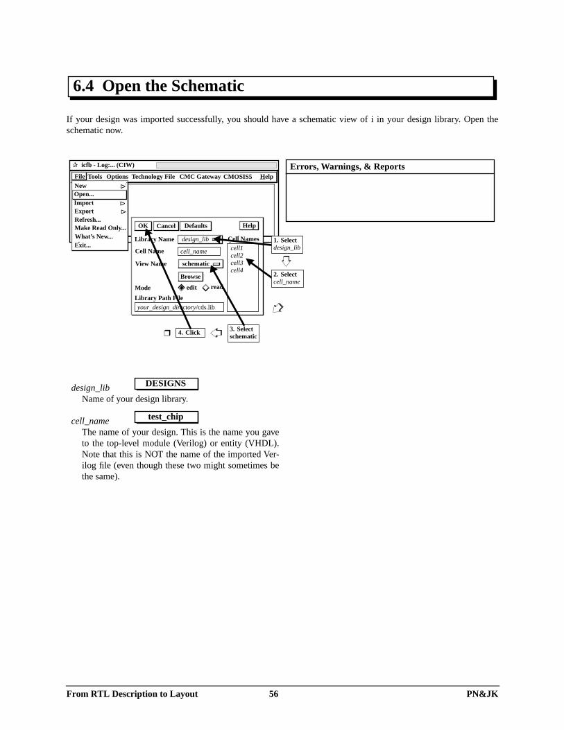
If your design was imported successfully, you should have a schematic view of i in your design library. Open theschematic now.
6.4 Open the Schematic
design_libName of your design library.
cell_nameThe name of your design. This is the name you gaveto the top-level module (Verilog) or entity (VHDL).Note that this is NOT the name of the imported Ver-ilog file (even though these two might sometimes bethe same).
DESIGNS
test_chip
Errors, Warnings, & Reports
4. Click❒
✰ icfb - Log:... (CIW)
CMOSIS5 Options Technology File CMC Gateway Tools Help FileNewOpen...Import
Refresh...Make Read Only...What’s New...Exit...
Export
∆
∆
∆
OK Cancel Help
Cell Name
design_libLibrary Name
Defaults
cell_name
schematicView Name
Browse
edit readMode
Library Path Fileyour_design_directory/cds.lib
cell1cell2cell3cell4
Cell Names
3. Selectschematic
1. Selectdesign_lib
2. Selectcell_name
From RTL Description to Layout 56 PN&JK

The schematic generated in Step 6.3 might have solders where wires (nets) cross. This will cause warnings when youcheck the design. Rather than modify the schematic, it is better to just disable these unimportant warnings.
6.5 Suppress Solder On CrossOver Warnings
Errors, Warnings, & Reports✰ Composer - Schematic Editing: ...
Tools Design Window Edit Help Add Check Sheet Mxd-Sig CMC Skill
Current CellviewHierarchy...Options...Rules Setup...
Schematic Monitors ∆
Label Attachment...Find Marker...Delete MarkerDelete All Markers...
OK Cancel
Percent Overlap Allowed
Defaults Apply Help
warningignored error
Logical Checks
warningignored error
Floating Nets
Offsheet Connector Check
NonePackaged Checks
warningignored errorFloating Input Pinswarningignored errorFloating Output Pinswarningignored errorFloating I/O Pinswarningignored errorFloating Switch Pinswarningignored errorShorted Output Pins
Physical Checks
warningignored errorUnconnected Wires
warningignored errorOverlapping Instanceswarningignored errorSolder On CrossOver
warningignored errorMaximum Label OffsetMax Distance from Wire
Name Checks
warningignored errorInstance/Net Name Collis-warningignored errorPin/Net Name Collision
warningignored errorInstance Name SyntaxInstance Name Expression
warningignored errorVerilog HDL Syntaxwarningignored errorVHDL Syntaxwarningignored errorAHDL Syntax
warningignored errorPin Name SyntaxPin Name Expression
warningignored errorNet Name SyntaxNet Name Expression
1. Turn ON
2. Click
❒
From RTL Description to Layout 57 PN&JK

As mentioned in Step 6.3, the schematic is currently composed of cells from the shadow libraries (i.e. _hcells and_cmcpads for cmosis5). You must now replace these cells with cells from the functional Cadence libraries (i.e. hcellsand cmcpads for cmosis5).
6.6 Replace Shadow Library Cells
• Warning: Unable to enter/create cellview...- Ignore these warnings
Errors, Warnings, & Reports✰ Composer - Schematic Editing: ...
Tools Design Window Edit Help Add Check Sheet Mxd-Sig CMC Skill
Layout/Extract ∆
Schematic ∆
RET ∆
P&R ∆ Check and Save Design Hierarchy
Check Supply IO
From RTL Description to Layout 58 PN&JK

Add power and ground bonding pads to the schematic. These will be used to connect power and to the chip. NOTE: This step is to be done twice, first to add power pads (select padvddrcc in Step 3), and then to add groundpads (select padvssrcc in Step 3).
6.7 Add Power Pads
1To place the selected component in the schematic, sim-ply left-click anywhere in the schematic editor window.But make sure that the component does not touch otherparts of the circuit.
Errors, Warnings, & Reports✰ Composer - Schematic Editing: ...
Tools Design Window Edit Help Add Check Sheet Mxd-Sig CMC Skill
Component...Wire (narrow)Wire (wide)Wire Name...
Note
∆
Pin...Block...Solder Dot
Show Categories
View
Messages
✰ Library Manager:
File Edit View Design Manager Help
abstractextractedlayoutschematicsymbol
Cell
padvddrccpadvddringpadvsscorepadvssrccpadvssring
Library
basiccdsDefTechcmcpadscmosis5designFlow
Hide Cancel Defaults Help
Library Name BrowseCell Names
Upsidedown
ColumnsArray
Rotate
Rows
Sideways
View NameInstance Names
1. Click
❒
2. Select cmcpads
3. Selectpadvddrcc
4. Selectsymbol
5. Click1
Repeat steps 3-5, but select padvssrcc in step 3.
From RTL Description to Layout 59 PN&JK

Use a CMC-provided script to verify that appropriate power/ground pads are included in the schematic. Make surethat you get the “IO check OK” report in the CIW.
6.8 Check Supply I/O
• Warning: Failed to open cellview...- Ignore these warnings
• Report: IO check OK.- If you don’t get this report in the CIW, then there is
something you have done wrongly. You shouldcorrect the mistake you made, or simply redo allthe steps from Step 6.3.
Errors, Warnings, & Reports✰ Composer - Schematic Editing: ...
Tools Design Window Edit Help Add Check Sheet Mxd-Sig CMC Skill
Layout/Extract ∆
Schematic ∆
RET ∆
P&R ∆ Check and Save Design Hierarchy
Check Supply IO
From RTL Description to Layout 60 PN&JK

Finally, check that the whole schematic is OK. Checking will also save the schematic if there are no errors. Again, ifterrors or warnings that you don’t understand are reported, you should not proceed. Some warnings (mentionedbelow) are normal and can be ignored.
6.9 Check and Save the Design Hierarchy
• Warning: Pin WORLD on ... floating ...- Ignore these warnings
Errors, Warnings, & Reports✰ Composer - Schematic Editing: ...
Tools Design Window Edit Help Add Check Sheet Mxd-Sig CMC Skill
Current CellviewHierarchy...Options...Rules Setup...
Schematic Monitors ∆
Label Attachment...Find Marker...Delete MarkerDelete All Markers...
1. Click
OK Cancel HelpDefaults
Ask Methose with errors
do not checkevery schematicProcess
View Name List
Apply
Referenced Libraries check
no
only those that need it
yesSave Schematics
SpectreS extracted schematic symbol
From RTL Description to Layout 61 PN&JK

7
In this step, you will layout the chip. First, the pads and gates are placed, and then the design is routed.
Place and Route the Design❒ Place and Rout the Design Using Cell Ensemble ❒
qdba c
clk
From RTL Description to Layout 62 PN&JK

From the schematic editor, open the design in a hierarchy browser, from where you will be able to create an autoLay-out view. NOTE that to launch the hierachy browser, the schematic editor menus must first be changed to Floorplan/Schematics menus.
7.1 Open the Design in a Hierarchy Browser
Errors, Warnings, & Reports✰ Composer - Schematic Editing: ...
Tools Design Window Edit Help Add Check Sheet Mxd-Sig CMC Skill
Analog ArtistDatapath/SchematicDesign SynthesisDiva
Simulation ∆
Floorplan/SchematicsMixed Signal Opts.Module MakerSchematics
∆
✰ Composer - Schematic Editing: ...
Tools Design Window Edit Add Check Sheet Floorplan CMC Skill He
OK Cancel Help
Library Name DESIGN
Defaults Apply
Cell Name test_chip
View Name schematic
Cross SelectCross Highlight
Hierarchy Browser...
1. Click
From RTL Description to Layout 63 PN&JK

Specify the names for global signals, i.e. global power signal name and global ground signal name.
7.2 Specify the Chip Global Signal Names
tech_libThe technology library, e.g. cmosis5, cmosp35, bic-mos, mitel15.
cmosis5
Errors, Warnings, & Reports✰ Hierarchy Browser: ...
Window Utilities Hierarchy Help
Cross SelectCross Highlight
Deselect All
Environment...
OK Cancel Help
======Display Options======
Defaults Apply
Instance Count On Node
Default Area Utilization (%) 80
Default Area Per Gate 10
Instance Node LabelInstance Filter
Fit Tree Graphics in Window
Tree Expansion DirectionTree Routes
instance namemaster nameIO core cell block
horizontalverticalfanlevered
======Expand Options======Levels
all1
======Generate AutoLayout/AutoAbstract Options======
Change Default Global Signal Names
simpleDefault Area Estimation Function
Obstruction On BlockHierarchy Delimiter Character
OK Cancel Help
Library To Store New Global Names
Defaults Apply
Global Power Signal Name vdd!
Global Ground Signal Name gnd!
Use Existing Global Names in Library
1. Click
❒
3. Click
2. Typetech_lib
From RTL Description to Layout 64 PN&JK

Create the autoLayout view.
7.3 Generate an AutoLayout View
• Report: The layout hierarchy has been createdsuccessfully.- If you don’t get this report in the CIW, then there is
something you have done wrongly. You shouldcorrect the mistake you made, or simply redo allthe steps.
Errors, Warnings, & Reports✰ Hierarchy Browser: ...
Window Utilities Hierarchy Help
Expand SelectedUnexpand SelectedGenerate Physical HierarchyGenerate Abstract From Symbol
∆ Properties
From RTL Description to Layout 65 PN&JK

Open the autoLayout into the Virtuoso layout editor. You do this from the Command Interpreter Window (CIW).ASfter a few seconds, the layout editor (shown in Step 7.5) should appear.
7.4 Open the AutoLayout
design_libName of your design library.
cell_nameThe name of your design.
DESIGNS
test_chip
Errors, Warnings, & Reports
4. Click❒
✰ icfb - Log:... (CIW)
CMOSIS5 Options Technology File CMC Gateway Tools Help FileNewOpen...Import
Refresh...Make Read Only...What’s New...Exit...
Export
∆
∆
∆
OK Cancel Help
Cell Name
design_libLibrary Name
Defaults
cell_name
schematicView Name
Browse
edit readMode
Library Path Fileyour_design_directory/cds.lib
cell1cell2cell3cell4
Cell Names
3. SelectautoLayout
1. Selectdesign_lib
2. Selectcell_name
From RTL Description to Layout 66 PN&JK

Cell Ensemble is the place and route engine that will be used to automatically place and route the design. You startCell Ensemble from the layout editor menus. Again, notice that the Cell Ensemble menus (shown in Step 7.6) areslightly different from the layout menus shown in this step.
7.5 Start Cell Ensemble
Errors, Warnings, & Reports✰ Virtuoso Editing: ...
Tools Design Window Create Help Edit Verify Misc CMC Skill
AbstractAnalog ArtistCompactorDevice-Level Editor
Microwave
∆
Device-Level RouterFloorplan/P&RInQueryLayoutLayout Synthesis
Module MakerPcellSimulation ∆
Structure-CompilerVerilog-XL
Block EnsembleCell Ensemble
Base Array Editor
Datapath/Cell EnsembleDatapath/Cell3 Ensemble
Cell3 Ensemble
Gate Ensemble
From RTL Description to Layout 67 PN&JK

Initialize the layout. This will place all the pads and gates outside th placement area. Because for small layouts thecore cells will have a small area relative to the area occupied by the pads, the aspect ratio is adjusted to reduce thisamount of “white space” around the core cells. Also, an aspect ratio of less than 1.0 results in a vertical core whichCadence can route more efficiently than a flat core. This is more significant for small designs.
7.6 Initialize the Layout
Errors, Warnings, & Reports✰ Virtuoso Editing: ...
Tools Design Window Create Route Edit Floorplan Place Analyze Help CMC
Reinitialize...I/O Place...PartitionBlock Place... ∆
Soft PinsUpdate AutoLayouts...Floorplan FileSynthesis Link
∆
∆
Replace View...
OK Cancel HelpDefaults Apply
Chip Aspect Ratio (Width/Height)Load a Floorplan File
Preserve pre-placed
Estimate Design Size
Initialize
IOs macros standard cellsspecial routing
lower leftChip Origin
File Name
final routingchip size instances statusregions groupsall none
Load a SDF File File Name
2. Click
❒
1. Type0.8
From RTL Description to Layout 68 PN&JK

In this step, you will place the pads and the standard cells automatically.
7.7 Place the Design
Errors, Warnings, & Reports✰ Virtuoso Editing: ...
Tools Design Window Create Route Edit Floorplan Place Analyze Help CMC
1. Click
IO CommandsAutomatic...Qplace...CTS Place...
∆
Spare Cell...Power CellGlue CellSnap To Grid...
∆ ∆
Sequencer...Check...
OK Cancel Defaults Apply Help
Method initial
Feedthru Master Name hft
Feedthru Library Name hcells
Placement Snap Grid 0.1
Feedthru Master View abstract
Mirror Cells
Insert Feedthru
Browse
Initial ImproveOptions
improve both
From RTL Description to Layout 69 PN&JK

Insert I/O corner cells. If you have not already done so, you should first copy the file glue.map from the technologysamples directory (this is usually /CMC/kits/technology/cadence/technology.version/samples) into your designdirectory. For the tutorial, make sure you are in your design directory and at the Unix prompt, execute the followingcommand:
cp /CMC/kits/cmosis5/cadence/cmosis5.2.3/samples/glue.map .
7.8 Insert I/O Corner Cells
Errors, Warnings, & Reports✰ Virtuoso Editing: ...
Tools Design Window Create Route Edit Floorplan Place Analyze Help CMC
IO CommandsAutomatic...Qplace...CTS Place...
∆
Spare Cell...Power CellGlue CellSnap To Grid...
∆ ∆
Sequencer...Check...
OK Cancel Defaults Apply Help
Net Association match TermName
Glue Cell Master Name
Glue Cell Library Name cmcpads
Terminal Mapping File
Glue Cell Master View abstract
Browse
none file
Justify...Add Corners...
Read Initial File...
3. Click
❒
1. TypeCORNERc
2. Type./glue.map
From RTL Description to Layout 70 PN&JK

Create the channels that will be used for routing the chip.
7.9 Create Routing Channels
Errors, Warnings, & Reports✰ Virtuoso Editing: ...
Tools Design Window Create Route Edit Floorplan Place Analyze Help CMC
1. Click
OK Cancel Defaults Apply Help
Initial Cut vertical
Channel Name Channels
Cut With Barriers
horizontal automatic
Remove Cutlines...Create...
Display Cutlines... ChannelsModify NetSpecial Net RouteGlobal Route
∆
Detail RouteSequencer...Check...
∆
∆
∆
∆
Delete
From RTL Description to Layout 71 PN&JK

Set the net properties from a file. There is a sample file in the Cadence directory, which should have been copied intoyour working directory. Make sure that this file is in the current directory, otherwise specify the full path to it in theFile Name field below. The sample file, called net.props, is in the same directory as the one used in Step 7.8.
7.10 Set Net Properties
Errors, Warnings, & Reports✰ Virtuoso Editing: ...
Tools Design Window Create Route Edit Floorplan Place Analyze Help CMC
4. Click❒3. Type./net.props
ChannelsModify NetSpecial Net RouteGlobal Route
∆
Detail RouteSequencer...Check...
∆
∆
∆
∆
OK Cancel Defaults Apply Help
Net Properties File write
Properties File Name
read
Net Properties File...Split Net
Modify Net Properties...
Unsplit Net
Nets all selected
Properties To Save P&R all
1. Turn ON
2. Turn ON
From RTL Description to Layout 72 PN&JK

Global signals include power and ground signlas. These signals have to be routed first.
7.11 Route the Global Signals
• Error: ..auiGetBoolFieldValue error..- Ignore this error.
Errors, Warnings, & Reports✰ Virtuoso Editing: ...
Tools Design Window Create Route Edit Floorplan Place Analyze Help CMC
1. Click
ChannelsModify NetSpecial Net RouteGlobal Route
∆
Detail RouteSequencer...Check...
∆
∆
∆
∆ Delete...
Single Net Global Route...
Automatic...
Interactive Global Route...
OK Cancel Defaults Apply Help
Method both
Automatic OptimizerOptions
optimizeauto
Display Channel Density...Remove Channel Density...Adjust Channel Density...Topology Display...Global Routing File...
From RTL Description to Layout 73 PN&JK

Now route all the other signals.
7.12 Route the Whole Chip
• Error: ..auiGetBoolFieldValue error..- Ignore this error.
Errors, Warnings, & Reports✰ Virtuoso Editing: ...
Tools Design Window Create Route Edit Floorplan Place Analyze Help CMC
1. Click
ChannelsModify NetSpecial Net RouteGlobal Route
∆
Detail RouteSequencer...Check...
∆
∆
∆
∆
OK Cancel Defaults Apply Help
Compaction Mode automatic
Max Horiz Jog Length for half-layer
Max Vert Jog Length for half-layer
Add Conditional Via
CompactOptions
rigid rigidIO
Reserve Tracks...Automatic...
Switch Layer...
Delete...Explode ChannelsStrip Outer Channels...
Contact Style centered offcentered pushed
Routing Layers 2 or 2 1/2 Layers 3 Layers
Tie Pin To Cell Instance
From RTL Description to Layout 74 PN&JK

Run the two CMC scripts. The first one ..., and the second one prevents bad shape errors on the VIA12 and VIA23instances when a DIVA DRC is performed..
7.13 Run the CMC Scripts
Errors, Warnings, & Reports✰ Virtuoso Editing: ...
Tools Design Window Create Route Edit Floorplan Place Analyze Help CMC
Layout/Extract ∆
Schematic ∆
RET ∆
P&R ∆
Flatten SymbolicViasSlot wide metal3 busses
✰ Virtuoso Editing: ...
Tools Design Window Create Route Edit Floorplan Place Analyze Help CMC
Layout/Extract ∆
Schematic ∆
RET ∆
P&R ∆
Flatten SymbolicViasSlot wide metal3 busses
From RTL Description to Layout 75 PN&JK
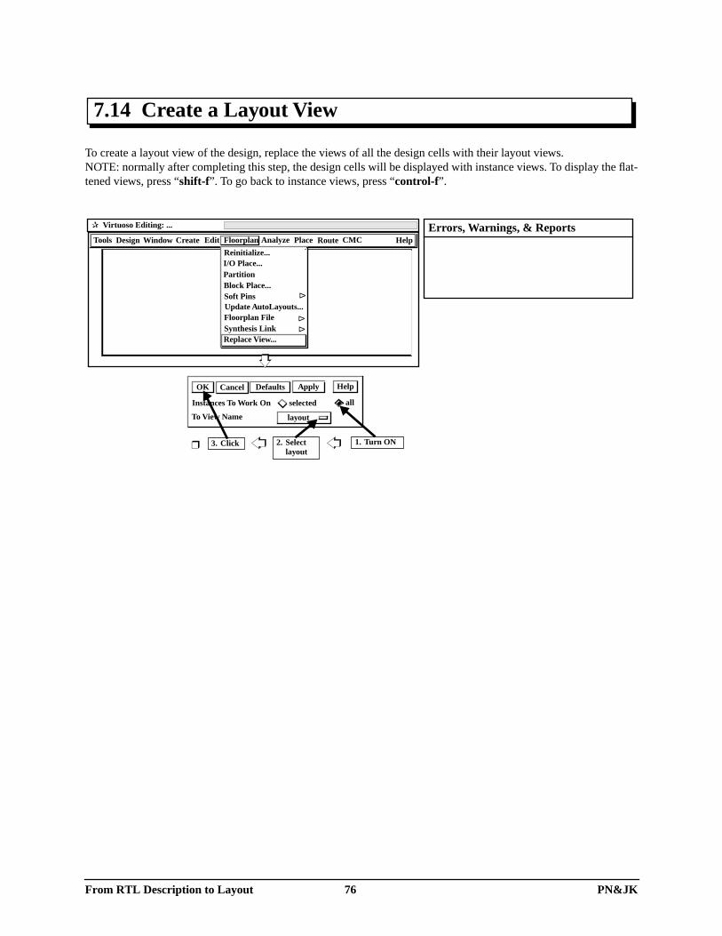
To create a layout view of the design, replace the views of all the design cells with their layout views. NOTE: normally after completing this step, the design cells will be displayed with instance views. To display the flat-tened views, press “shift-f”. To go back to instance views, press “control-f”.
7.14 Create a Layout View
Errors, Warnings, & Reports✰ Virtuoso Editing: ...
Tools Design Window Create Route Edit Floorplan Place Analyze Help CMC
3. Click❒ 2. Selectlayout
1. Turn ON
Reinitialize...I/O Place...PartitionBlock Place... ∆
Soft PinsUpdate AutoLayouts...Floorplan FileSynthesis Link
∆
∆
Replace View...
OK Cancel Help
layoutTo View Name
Defaults Apply
Instances To Work On selected all
From RTL Description to Layout 76 PN&JK

You must save both the autolayout and layout views of the design. If you want to re-run the aouto place and routeagain, you do it on the autolayout view. Otherwise the remaining steps, Design Rule Checking (DRC) and LayoutVersus Schematic (LVS) will be done on the layout view. After this step, you may close the autoLayout editorwindow.
7.15 Save the Design
Errors, Warnings, & Reports✰ Virtuoso Editing: ...
Tools Design Window Create Route Edit Floorplan Place Analyze Help CMC
2. Click❒1. Type
layout
SaveSave As...Discard EditsLoad...
∆
Make Read OnlyShow Selected...HierarchyPlot
∆
∆
OptionsEnvironment ∆
✰ Virtuoso Editing: ...
Tools Design Window Create Route Edit Floorplan Place Analyze Help CMC
SaveSave As...Discard EditsLoad...
∆
Make Read OnlyShow Selected...HierarchyPlot
∆
∆
OptionsEnvironment ∆
OK Cancel Help
Library Name DESIGN
Defaults Apply
Cell Name test
View Name layout
From RTL Description to Layout 77 PN&JK
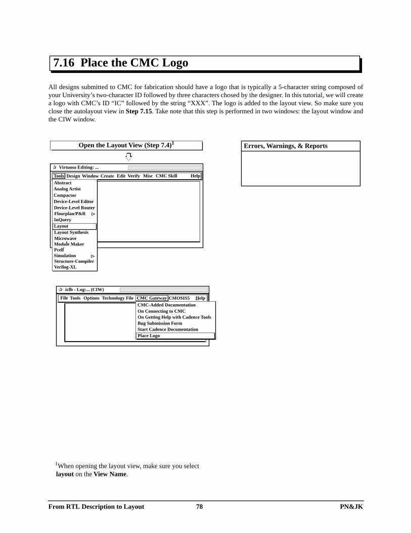
All designs submitted to CMC for fabrication should have a logo that is typically a 5-character string composed ofyour University’s two-character ID followed by three characters chosed by the designer. In this tutorial, we will createa logo with CMC’s ID “IC” followed by the string “XXX”. The logo is added to the layout view. So make sure youclose the autolayout view in Step 7.15. Take note that this step is performed in two windows: the layout window andthe CIW window.
7.16 Place the CMC Logo
Errors, Warnings, & Reports
1When opening the layout view, make sure you select layout on the View Name.
Open the Layout View (Step 7.4)1
✰ Virtuoso Editing: ...
Tools Design Window Create Help Edit Verify Misc CMC Skill
AbstractAnalog ArtistCompactorDevice-Level Editor
Microwave
∆
Device-Level RouterFloorplan/P&RInQueryLayoutLayout Synthesis
Module MakerPcellSimulation ∆
Structure-CompilerVerilog-XL
✰ icfb - Log:... (CIW)
CMOSIS5 Options Technology File CMC Gateway Tools Help File
On Connecting to CMCOn Getting Help with Cadence Tools
CMC-Added Documentation
Bug Submission FormStart Cadence DocumentationPlace Logo
From RTL Description to Layout 78 PN&JK

From RTL Description to Layout 79 PN&JK