teaching guide: electronics - aqa
TRANSCRIPT

1
Teaching guide: Electronics
This booklet provides background material for teachers preparing students for the Electronics option of the AQA A-level Physics specification. It amplifies specification topics with which teachers may not be familiar and should be used in association with the specification. The booklet is not intended as a set of teaching notes.
This guide should help teachers answer questions in class and extend brighter students. Sometimes this has meant going beyond the specification. Anything that is not explicitly mentioned in the specification is printed on a light background tone.

2
Contents Introduction ........................................................................................................... 3
Chapter 1 Discrete semiconductor devices ................................................................. 4
A. The MOSFET (Metal Oxide Semiconductor Field Effect Transistor) ........................ 4
B. The Zener diode ............................................................................................. 6
C. The Photodiode .............................................................................................. 8
D. The Hall effect sensor ................................................................................... 10
Chapter 2 Analogue and digital signals .................................................................... 12
A. Differences between analogue and digital signals .............................................. 12
B. Definition of terms ......................................................................................... 13
C. Analogue sensors ......................................................................................... 14
D. Analogue-to-digital conversion ........................................................................ 15
Chapter 3 Analogue signal processing ..................................................................... 19
A. The LC resonant filter .................................................................................... 19
B. The ideal operational amplifier ........................................................................ 25
Chapter 4 Operational amplifier circuits.................................................................... 28
A. The inverting amplifier ................................................................................... 28
B. The summing amplifier .................................................................................. 30
C. The non-inverting amplifier ............................................................................. 30
D. The difference amplifier ................................................................................. 31
E. Real operational amplifiers – their limitations..................................................... 33
Chapter 5 Digital signal processing ......................................................................... 36
A. Combinational logic circuits ............................................................................ 36
B. Sequential logic circuits ................................................................................. 44
C. Astables ...................................................................................................... 48
Chapter 6 Data communication systems .................................................................. 52
A. Principles of Data communication systems ....................................................... 52
B. Transmission media ...................................................................................... 53
C. Multiplexing ................................................................................................. 60
D. Amplitude & frequency modulation .................................................................. 61
E. Pulse Code modulation (PCM) ........................................................................ 66
Teacher Resource Bank ........................................................................................ 68
Equipment & materials resources: ....................................................................... 68
General resources ............................................................................................ 68
Chapter 1 Discrete semiconductor devices (specification reference 3.13.1) ............... 69
Chapter 2 Analogue and Digital signals (specification reference 3.13.2) .................... 70
Chapter 3 Analogue signal processing (specification reference 3.13.3) ..................... 70
Chapter 4 Operational amplifier circuits (specification reference 3.13.4) .................... 71
Chapter 5 Digital signal processing (specification reference 3.13.5) .......................... 71
Chapter 6 Data communication systems (specification reference 3.13.6)................... 72

3
Introduction
The Electronics Option offers a contextual framework to some of the core physics principles studied in earlier parts of the specification, for example in the electricity and waves sections. As well as showing how these principles are used in practical ways, the Option gives some insight into how some modern electronic devices and systems work.
These guidance notes therefore include application examples throughout. Through this approach students may find that this specialised branch of the physical sciences – a key component of electrical engineering – is something that they wish to pursue further.

4
Chapter 1 Discrete semiconductor devices
Students should understand the difference between discrete components and integrated circuits.
A discrete component generally consists of one semiconductor device (eg one transistor, one diode). An integrated will consists of several individual devices, interconnected on a single wafer or chip of silicon. There can be a large number of devices in a single integrated circuit: the processor chip in a typical desk-top
computer for example, will contain in excess of 3 × 10¹⁰
devices.
It is possible to fabricate passive devices in silicon (eg resistors, capacitors) as well as active devices, so that integrated circuits can perform complex functions with relatively few external components.
The devices chosen for this Option are used in many electronic systems. In all cases, knowledge or understanding of the physics of the device (ie the scientific principles determining how they behave) is not required, only their function.
A. The MOSFET (Metal Oxide Semiconductor Field Effect Transistor)
The device which has made all modern electronics possible is the transistor. There are several different types of transistor, but the MOSFET is now the most commonly used type given its versatility and efficiency. As with many discrete devices, the MOSFET comes in a variety of versions. Only the N-channel enhancement mode device is required for this Option.
A simplified structure of the MOSFET is shown. Note the presence of the two p-n junctions.
In operation, a voltage on the gate G creates an electric field in the p-type material, the effect of which is to create an n-type channel through which current flows between drain D and source S. An important characteristic of these devices is that, due to the SiO2 insulating layer between the gate connection and the p-type substrate, the resistance between the gate and the other electrodes is extremely high
(typically > 1011
Ω). Thus, the MOSFET draws effectively zero current from a circuit connected to its gate.

5
The MOSFET will turn on when the voltage VGS between the MOSFET gate and
source exceeds a threshold value. This is usually given the symbol VGS(th) or Vth and
is typically between 1 V and 2.5 V. This is the gate voltage at which the n-type
channel is just closed, and so the device is just off. (It is sometimes called VP,
standing for ‘pinch-off’, only Vth will be used in assessments).
Two sets of characteristic curves are normally used to describe the behaviour of the MOSFET.
IDSS is the drain current which flows when the gate voltage is zero (and the device should therefore be fully off), and is an important value for designers. Like all
transistor parameters it changes with temperature. Vth will typically fall by 8 mV K-1
as the device temperature increases. Students will be expected to be able to interpret the key features but not recall details of the graphs.
A MOSFET can be used as an electronic switch. A high-current device, such as a heater or solenoid, can be turned on by a low-power signal from a logic system. A typical arrangement might be as shown below.
The output current of the MOSFET IDS, which turns on the solenoid, could be large,
yet no current is drawn from the output of the logic system.
VDS is the voltage between the drain and the source. Students should understand why this voltage changes between the MOSFET being off and on. When the
MOSFET is off, IDS is zero, and so no voltage is dropped across the solenoid. The
value of VDS is thus the solenoid supply voltage – in this case 28 V. When the
MOSFET is on, it behaves as a very low resistance – much lower than the resistance of the solenoid in this case. Thus by potential-divider action, VDS will be
approximately zero, and the solenoid will have 28 V across it and be fully energized.

6
There is a protection diode across the solenoid which is needed whenever the component being turned on by the MOSFET is inductive. Lenz’s law (spec. 3.7.4.4) predicts that when the MOSFET turns off, the sudden reduction in current will lead to a large voltage across the coil to attempt to keep the field constant. This may cause the MOSFET to fail. The diode short-circuits the coil when this happens, protecting the transistor from damage. In teaching this area, careful consideration of the direction of the induced emf is important.
Because of its very high input resistance, the MOSFET is susceptible to electrostatic charge build-up at the gate, and can turn on partially or fully when the gate is
unconnected (‘floating’). To prevent this, a resistor RG can be connected between the
gate and 0 V to ensure that even if the input signal is disconnected the MOSFET will
not turn on. RG should be high, so as to not draw significant current from the input
signal; 1 MΩ is a typical value.
B. The Zener diode
The V-I characteristic of a p-n junction diode is covered in the Electricity section of the specification (3.5.1.2). This is a good starting point to remind students of the behaviour where the diode ‘breaks down’ at a high value of reverse voltage –
typically 50 V. The construction of an ordinary diode is optimized to ensure VBR is as large as possible.
A Zener diode is also a p-n junction diode, but with the semiconductor material heavily doped so that its reverse breakdown voltage is much smaller and takes a specific value. By doing this, the Zener diode can be used as a constant voltage source to provide a fixed reference voltage to a circuit or system. The characteristic
is thus similar to the ordinary p-n junction diode and is shown for a typical 5.6 V device.
There are three key things to notice in this diagram:
The Zener diode symbol shown is the generally accepted standard, but the alternative one shown is also acceptable
The forward characteristic (VZ positive) is roughly the same as for an ordinary diode
The reverse breakdown voltage (VZ negative), becomes almost independent of
the reverse current IZ, once IZ is more than 5 mA or so. This is called the
minimum Zener current, IZ (min).

7
When used as a constant voltage source, or voltage reference, the Zener diode is connected as shown below (note the diode polarity). Students should understand how this circuit works.
Ignoring temperature effects, VOUT stays at the value VZ, whatever the value of VIN, provided:
VIN > VZ
IZ is ≥ about -5 mA, and remains constant
no current is drawn from the output of the circuit.
A typical application of the Zener diode is for sensing, where the output from, say, the oil temperature sensor in a car is compared with a fixed voltage; if the oil temperature exceeds a pre-set safe value, a dashboard warning light is to be turned on:

8
The value of R is calculated knowing the values of VIN and VZ. For example, if the
temperature sensor signal at dangerous oil temperatures is above 5 V, then a 5.1 V
Zener diode would be suitable. Car battery voltage can vary between about 10 V and
14 V. Since the lowest Zener current which will occur at the lowest battery voltage
must be at least 5 mA, then –
Ω.
Students may suggest that this can be done using a simple potential divider: the answer is that it can. A useful exercise to test students’ understanding is to ask them to compare the Zener diode solution with the potential-divider solution.
C. The Photodiode
The photodiode is a light-to-electricity converter and is another variant on the p-n junction diode. The p-n junction of the photodiode will generate a current when exposed to light as photons are absorbed and charge carriers are released at the junction, leading to charge flow. This can occur at all p-n junctions (which is why transistor and diode encapsulation is light-tight). In the photodiode the junction is deliberately exposed using a transparent window or lens to capture light. In special cases an optical fibre is embedded in the device with its termination at the junction, to enhance the effect. Solar cells are photodiodes with very large exposed junctions, or arrays of junctions.

9
A typical photodiode characteristic, showing how the photodiode current varies with light level, is shown below.
The photodiode can be operated in one of two main modes: photovoltaic, and photoconductive. Photovoltaic mode is used for solar cells – hence the commonly used name of Solar PV for solar panels. In electronics photodiodes are usually operated in photoconductive mode, where the diode is reverse-biased. The characteristic for these two regions is shown below.
The photoconductive mode is preferred for two main reasons: the relationship between photodiode current ID and light intensity is very linear, and the response
time is much smaller (and is smaller the larger the value of reverse bias).
The dark current, which flows even when there is no light falling on the p-n junction,
is typically of the order of 500 pA. The responsively of the photodiode, the size of
current for a given light intensity, is typically 0.6 A W–1
(sometimes quoted in
μA mW–1
).
Photodiodes are manufactured for a range of different light wavelengths, from far infrared through to ultraviolet. The curve below shows a typical spectral response curve for an infrared device. For this device, peak sensitivity is about 0.6 A W
–1.

10
A common use of the infrared photodiode is as the detector for the receiver of an optical fibre.
Students will be familiar with the light dependent resistor (LDR) from their work on potential dividers in the core syllabus.
D. The Hall effect sensor
Accurate magnetic field measurements are important in the physical sciences, in equipment that uses magnetic fields (the MRI scanner), and in geology and prospecting. The detection of the presence or otherwise of a magnetic field can be used in contact-less switches and proximity detectors.
The Hall effect sensor is essentially a magnetic field-to-voltage converter. It consists of a single ‘slab’ of semiconductor through which a current is passed.
Students will have learned about the forces on current-carrying conductors in magnetic fields (3.7.4.4). The charge carriers passing through the semiconductor are deflected under the influence of an external magnetic field. This has the effect of creating a potential difference, called the Hall voltage, between the sides of the semiconductor perpendicular to the direction of current flow, as shown.
The Hall voltage VH is linearly related to the strength of the applied magnetic field
provided the current (and therefore drift speed) remains constant. The relationship
between magnetic field strength and output voltage is given by (
) where
RH is the Hall effect coefficient, I the current in the sensor, t the thickness of the
substrate and B the applied magnetic flux density.

11
The Hall voltage is usually small – a matter of a few μV even for sizeable fields. For this reason, most commercial devices include a built-in amplifier. The output for a
typical amplified device is around 30 mV mT–1
. The Earth’s magnetic field is about
0.05 mT and so would produce an output of around 1.5 mV.
It is easy to demonstrate a device (eg SS495A2) detecting the direction of the Earth’s magnetic field using an oscilloscope or multimeter. Gallium arsenide (GaAs) is often used for the semiconductor devices which are often very small.
As well as being used to measure the strength of a magnetic field, the Hall effect sensor is frequently used with additional electronics to cause the device to turn its output fully on when the field strength exceeds a pre-set threshold value – in other words as a proximity switch. This is often found in engine-management systems in cars, used in conjunction with a magnet to measure the speed of rotation of the engine or other rotating component.
The output of the sensor will be a pulsed signal, the frequency of which represents the speed of the rotating component.
The Hall effect sensor has many advantages over a conventional switch as it:
is more reliable as there are no moving parts
is much faster – operating at rates typically up to 100 KHz
does not suffer from contact bounce
is unaffected by environmental conditions (eg moisture or corrosion)
can be used where conventional switches pose danger eg, in the level sensing system for a fuel tank.

12
Chapter 2 Analogue and digital signals
In this chapter we examine the differences between analogue and digital systems. Students need to understand these differences fully, as many electronic systems have examples of both types with conversions from one type to another.
A. Differences between analogue and digital signals
Analogue signals represent ‘real-world’ quantities. Daylight intensity can, for example, take any value – between zero (pitch darkness) and a high value in bright sunshine, and an infinite number of possible levels in between. A light sensor, such as an LDR or photodiode, will therefore produce an electrical signal which can change continuously between low and high. Such signals are analogue, as is the signal from a microphone, as shown below.
Digital signals can only have discrete values, and nothing between these values. A signal that can be 2 V, 3 V, 4 V or 5 V – but nothing else – is therefore digital. We have come to regard digital signals however as those with only two possible values,
eg 1 V and 7 V. The reason for this is that these two values allow the representation of numbers in binary form – and this has enabled the development of the digital computer. In this guide a digital signal is taken to be one having only two levels. The signal from a push-button switch is an example of this, as shown below.
The digital signal can of course have any two different voltages for the two levels.
However, one level is often the supply voltage of the system and the other 0 V. In many student projects the supply will be a 9 V battery. The two levels for the digital
signals in this system will thus be 0 V and 9 V. In computers and in many other
pieces of equipment the supply for the digital circuits is usually 5 V (and for
processor chips typically 3 V, with recent processors working down to 1.8 V). Generally speaking, the lower the voltage, the faster operation of the circuits.

13
B. Definition of terms
a. Analogue
Size is the main parameter of an analogue signal.
The graph below shows an analogue signal, with its size indicated in two ways, Vpk
and Vpk-pk.
However, these parameters can often be difficult to specify, because a typical signal, like that shown, can swing between either polarity, and tends to average to zero over time.
Vpk peak voltage; the magnitude of the positive half of the signal voltage.
Vpk – pk peak-to-peak voltage; the value of signal voltage between the extremes of its
positive and negative halves.
For signals like this it is usual to use the r.m.s. (root-mean-square) value of the wave to indicate its size, or amplitude.
A note of caution must be given here. The relationship between the peak value and the r.m.s. value for a sine wave (3.7.4.5) is only true for a sine wave, and not for another wave shape. If the signal is periodic and symmetrical, such as a sine wave,
then we would normally use the value of Vpk to define the amplitude of the wave.
b. Digital
With digital signals, the absolute value (voltage) of the signal is immaterial; what matters is which level it is at. We commonly refer to the two states of a digital signal as being either ON and OFF (HIGH/LOW, or TRUE/FALSE or 1 and 0).
Digital signals can represent numbers in binary (or base-2). Whilst students are not expected to be able to manipulate binary numbers or perform binary arithmetic, it is nevertheless useful, for an understanding of what follows later, to teach some of it.

14
A group of eight digital signals, eg 10011011 is called a byte . Each signal within the byte is called a bit (from binary digit). As for any number base, the position of a digit in the number is significant, and in the case of binary will be increasing powers of 2. Thus:
Hence 100110112 is equal to 15510
Digital signals are used in:
combinational logic circuits (see chapter 5A), where ‘decisions’ are made on the state of various input signals, and one or more output signals are turned on or off accordingly
sequential logic circuits (see chapter 5B), which are predominantly to do with counting and pulse generating/handling.
C. Analogue sensors
Students should be aware of and familiar with a broad range of analogue sensors (ie devices that provide an electrical signal in response to the presence of some physical quantity. As well as the microphone, LDR, photodiode and Hall effect device mentioned earlier the list could include:
thermistor (temperature)
accelerometer (acceleration)
pressure sensor
moisture sensor
pH probe
strain gauge (mechanical deflection)
lambda sensor (oxygen; used in car engine management systems).
Not all analogue sensors actually produce a signal voltage in their own right. The LDR and thermistor are two examples; the ‘signal’ with these is a resistance change, and additional circuitry is required to turn this into a voltage or current.

15
D. Analogue-to-digital conversion
We are usually interested in processing real-world signals – analogue – yet the digital computer is most commonly used for processing data. So, signals often have to be converted from one to the other by an A-D Converter, often called by its acronym ADC.
The basic principle of an ADC is to sample the analogue signal, convert it into a binary number representing its instantaneous amplitude, and then repeat that process. This produces a regular sequence of numbers that represent the time variation of the amplitude of the signal.
Two parameters affect how well an analogue signal can be represented:
sampling rate - how frequently the signal is sampled
resolution - the range of numbers used to represent the amplitude.
The diagrams below show the process.
This process of converting an analogue quantity into a sequence of numbers is called quantisation. The resulting number sequence is called the digitised signal.
Although not required by the specification, the picture should be completed by mentioning conversion in the other direction. It is often necessary to turn a signal back into an analogue signal so that it once again becomes a ‘real world’ signal can be used. This reverse process is performed by a D-A Converter, again, called by its acronym DAC.
A very good example of a complete system which uses both ADCs and DACs is the production and use of audio CDs.
The diagram of the ADC operation above shows that a quantised signal can be very ‘lumpy’. This is partly due to the fact that it is being sampled too infrequently; but also

16
due to the fact that there is an insufficient number of levels to represent it – in this example just 8 (three-bit numbers).
Students should have a clear understanding of how sampling rate and resolution affect the overall quality of the conversion.
a. Sampling rate
When the sampling rate is too small, then chunks of signal variation will be missed. If a major change of analogue signal occurs between two samples then the digital number sequence will not be a faithful representation of the original.
On the other hand, if the sample rate is too high then the electronics required to do the conversion become overly complex, and, crucially, the bandwidth increases.
In 1928 Nyquist showed that the original analogue signal can be completely and faithfully recovered from its digitised version when it is sampled at a rate of at least twice the maximum frequency present in the signal. This maximum frequency is called the Nyquist Frequency, and the sampling rate is called the Nyquist Rate Nyquist rate = 2 × Nyquist frequency. The accepted range of frequencies for audio is 20 Hz–20 kHz; digitisation of an audio signal should be sampled at a rate of at least 40 kHz. The standard frequency that is used in practice is 44.1 kHz (some ultra-high quality systems sample at up to 192 kHz).
If there are any frequencies present in a signal which are greater than the Nyquist frequency then they may still be sampled, but will become corrupted. This results in an effect called aliasing, which introduces distortion into the signal.
In the top graph the Nyquist frequency of the signal is well below the sampling rate, and thus complete and distortion-free recovery should be possible. In the lower graph the frequency is much greater than the sampling rate; the result is the inclusion in the resulting signal of the low frequency component shown. This is an ‘alias’ of the original signal, hence the name given to this effect.
To avoid this problem it is common practice to precede the ADC with a low-pass filter, which cuts off all frequencies above those at the Nyquist frequency. This is called an anti-aliasing filter.
To demonstrate the principle of aliasing, use a vibrating, stretched string on which a standing wave has been set up. When the standing wave on the string is ‘sampled’ (ie illuminated) by a stroboscope, flashing at a rate which is a sub-multiple of the string vibration frequency, then the low-frequency aliased ‘signal’ becomes visible.
17
b. Resolution
The number of bits in each sample determines the resolution of the quantisation process – ie the smallest change in analogue input signal which will result in a change of digital output signal. In the example shown earlier the conversion is performed to 3-bit resolution. This means that, including zero, there are 23 or 8 possible values of converted signal. If the analogue signal is 6 V peak as shown,
then the smallest change that can be converted is 6/23 or 0.75v. This is clearly too
crude for most practical purposes: 8 bits is generally regarded as a minimum (but i t does depend, of course, on the required characteristics of each particular system).
This would give a resolution of 1 in 256 or about 23 mV in the case of the 6 V maximum.
For CD systems like the one shown on page 21, conversion is commonly 16-bit, with “Super Audio CD” (SACD) systems converting to 24-bits.
Students should understand the process of determining the resolution of the conversion process given the number of bits used.
Advantages of digital sampling
There are several compelling reasons why we bother to convert to digital from a good analogue signal, then back again, with all the errors that this can introduce.
Digital signals can be much easier to process and to save than analogue counterparts. Digital filters, where the filtering of the signal is done by computation, can be more sophisticated and much more accurate than analogue techniques.
Once converted, the digital signal can be easily saved in memory or to disk for later, easy retrieval. Analogue recording methods, such as tape and vinyl disc for audio signals, have many associated problems, not least the introduction of noise and signal loss.
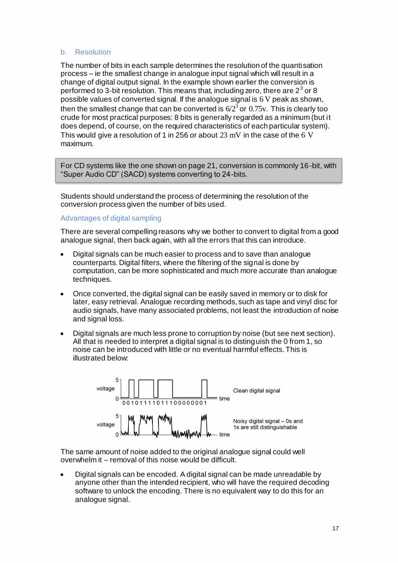
Digital signals are much less prone to corruption by noise (but see next section). All that is needed to interpret a digital signal is to distinguish the 0 from 1, so noise can be introduced with little or no eventual harmful effects. This is illustrated below:
The same amount of noise added to the original analogue signal could well overwhelm it – removal of this noise would be difficult.
Digital signals can be encoded. A digital signal can be made unreadable by anyone other than the intended recipient, who will have the required decoding software to unlock the encoding. There is no equivalent way to do this for an analogue signal.

18
A single data link can easily be used by many different data sources, with no risk of them getting confused. By encoding each data stream differently the receiving end can distinguish between them. Thus it is possible to send many thousands of telephone calls down an optical fibre, and to extract and separate them at the other end.
However, a disadvantage of digital sampling is that a digital signal will often require a greater bandwidth than its analogue equivalent.
Consider the example of the CD system on page 21.
The bandwidth of the original audio signal is 20 kHz, so it will need to be sampled at
a rate of 40 kHz (at least) before conversion. This means one sample every 1 / (40 × 10
3 2 μs.
(i) For 16-bit conversion, a stream of sixteen 0 s and 1 s will be generated for each
sample. If we look at the case where this stream happens to be alternate 0 and 1 then we have:
(ii) The stream of bits lasts for 2 μs, so this wave will have a period of 2 μs / 8 or
just over 3 μs, giving it a fundamental frequency of around 320 kHz.
So, the transmission medium is going to require a bandwidth 16 times that of the original analogue signal. Signal compression techniques can be employed to reduce this, eg digital audio compression standards such as MP3.
c. Recovery of digital signals from noise
Noise added to a digital signal during transmission will cause problems if it is severe. Also, too much attenuation occurs, it may be difficult for the system to distinguish
between 0 and 1.
Two methods are used to mitigate the effects of noise on digital signals.
(i) Repeaters
These amplify a weakened signal:
(ii) Regenerators
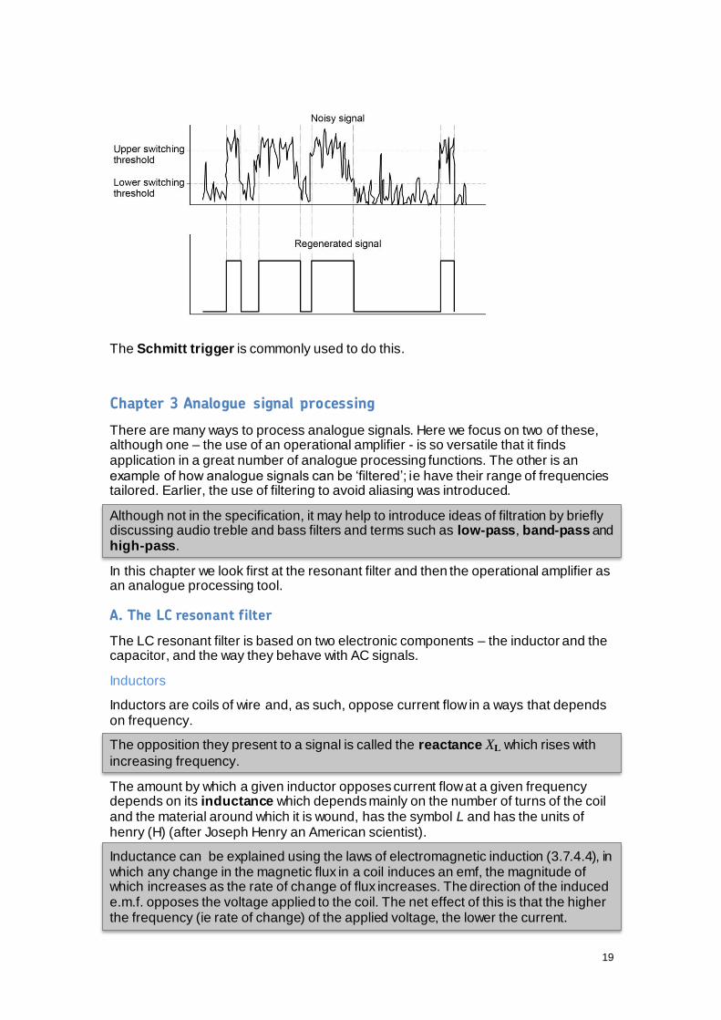
These regenerate a noisy signal:
Regenerators use a switching circuit with hysteresis. It switches on when the input signal is at the upper switching threshold and switches off when the signal has drops below the lower switching threshold.
19
The Schmitt trigger is commonly used to do this.
Chapter 3 Analogue signal processing
There are many ways to process analogue signals. Here we focus on two of these, although one – the use of an operational amplifier - is so versatile that it finds application in a great number of analogue processing functions. The other is an example of how analogue signals can be ‘filtered’; ie have their range of frequencies tailored. Earlier, the use of filtering to avoid aliasing was introduced.
Although not in the specification, it may help to introduce ideas of filtration by briefly discussing audio treble and bass filters and terms such as low-pass, band-pass and high-pass.
In this chapter we look first at the resonant filter and then the operational amplifier as an analogue processing tool.
A. The LC resonant filter
The LC resonant filter is based on two electronic components – the inductor and the capacitor, and the way they behave with AC signals.
Inductors
Inductors are coils of wire and, as such, oppose current flow in a ways that depends on frequency.
The opposition they present to a signal is called the reactance XL which rises with
increasing frequency.
The amount by which a given inductor opposes current flow at a given frequency depends on its inductance which depends mainly on the number of turns of the coil and the material around which it is wound, has the symbol L and has the units of henry (H) (after Joseph Henry an American scientist).
Inductance can be explained using the laws of electromagnetic induction (3.7.4.4), in which any change in the magnetic flux in a coil induces an emf, the magnitude of which increases as the rate of change of flux increases. The direction of the induced e.m.f. opposes the voltage applied to the coil. The net effect of this is that the higher the frequency (ie rate of change) of the applied voltage, the lower the current.

20
XL is not a simple resistance. However, because for a given value of inductance and at a given frequency of applied voltage the ratio of voltage to current flow is a
constant, reactance is also given the units of ohm. The value of XL at a frequency f
and for an inductor of value L is 2 . The variation with frequency of XL for an
inductance of μH is shown.
Capacitors
The core syllabus (3.7.3.1) treats capacitors in terms of their behaviour at dc. Capacitors are subject to ac signals and need to be considered differently.
Students will know from plotting charging and discharging curves for RC circuits that the charge on a capacitor cannot be changed instantaneously. If a voltage is suddenly applied across the capacitor a large initial current flows. In fact the greater the rate of voltage change, the greater the initial current.
For ac, a capacitor exhibits lower opposition to current flow the greater the frequency of applied voltage. As with the inductor, this opposition is called reactance with the
symbol XC. Again, for given values of capacitor and frequency, the ratio of applied voltage to current flow is a constant takes the unit: ohm.
The value of XC at a frequency f and for a capacitor of value C is
2 . The
graph below shows the relationship between the reactance XC and frequency for a
capacitance of 22 nF.

21
The frequency dependences of XL and XC mean that inductors or capacitors can be
used in filter circuits by themselves.
The parallel LC circuit
Consider the circuit shown below, where VIN is an applied ac signal and IIN is the
current that results.
This is called a parallel LC circuit. The behaviour of this circuit is frequency dependent. How does it vary with frequency?
Consider very low frequencies. At these frequencies XL will be small and XC will be
large. Thus the net reactance will be very low. At very high frequencies, the situation reverses. Now XC will be small, whilst XL will be large. Again, the net reactance will
be very low.
At intermediate frequencies the behaviour changes: Overlapping the XC and XL
graphs makes it clear that at one frequency XL = XC.

22
At this frequency, energy in the circuit transfers back-and-forth between the capacitor and the inductor, continuously – the circuit resonates. No net current enters or leaves the circuit, and the circuit appears to be exhibit infinite reactance. This
frequency is called the resonant frequency f0.
This leads to a filter. Consider the circuit with R and the parallel combination of XL
and XC . The circuit resembles a potential divider with R and L+C.
These reactances are not resistances and the potential-divider equation cannot be used to quantitatively determine the relationship between VOUT and VIN without
considering the phase. But, qualitatively, potential divider ‘action’ does occur, and we can conclude:
at f0 (resonance), where the net reactance is at a maximum, VOUT VIN.
at the two frequency extremes, where the net reactance ≈ 0, VOUT .

23
The complete frequency response is shown.
The resonant filter circuit can thus or select a narrow range of frequencies. It finds a major use in radio reception, where it is used to select a particular radio broadcast. It is then given the name tuned circuit, and is the central part of a receiver’s tuner. In such an application, either the capacitor (or sometimes the inductor) is variable so that the user can tune different stations. This is dealt with in more detail in Chapter 6.
Of crucial importance is the value of f0 for a given L and C. At resonance, XL = XC
and therefore 2
2 . Re-arranging gives
2 . For the C and L values
given on the graph this equates to 107.3 kHz as confirmed by the curve. The width of
the resonance peak for the LC resonant filter is of importance for an application. If a
circuit is meant to filter a 50 Hz mains hum then the narrower the better.
As a measure of this, the Q factor (Quality Factor) is used. This is defined as
where f0 is the resonant frequency of the filter and fB is the bandwidth of the filter at
the ½ power points.
From the graph, fB is read off as 29.6 kHz, giving a Q factor of approximately 3.6.
Note that it is at the ½ power (or energy) points that fB is determined, which means
that on a voltage–frequency graph, it must be measured at
√ or 0.71 of the peak
value.

24
What affects the value of Q?
In a real LC resonant circuit, energy is lost during resonance. This happens mainly in the resistance (not reactance) of the coil. As it is likely to be made of many turns of wire, this resistance may be large. So, as energy transfers repeatedly between
inductor and capacitor, some is lost as internal energy in the coil ( I2R losses). The
capacitor too has some resistance and therefore a leakage current. The total effect
loss is called damping, which reduces Q, and means that the net reactance of the
LC parallel circuit will be lower than expected at the resonant frequency. Because
main losses tend to be in the coil, inductor data sheets often quote Q for the coil itself.
Comparison of the LC resonant circuit with the mass–spring system
Students will have met the concept of resonance in the Simple Harmonic Motion and Forced Vibrations parts of the specification (3.6.1.3/4). This considers resonance in terms of the mass–spring system. There are close analogies between this and the LC circuit.
For the mass–spring system, students will be familiar with the relationship between
the oscillation period T, the spring stiffness k and the mass m, 2
Since T =
, this can be written as
2
. This is similar to the equation for the
resonant frequency of the parallel LC circuit
2 from which we deduce that:
.
In the LC circuit the inductor easily transfers energy at a slow rate, but exhibits
increasing opposition to this transfer as frequency increases. Similarly, in the mass–spring system the mass can be moved to-and-fro slowly, transferring energy, but exhibits increasing resistance to motion as the speed – and acceleration – increases.
So, increasing the mass in the mass–spring system, and increasing the inductance in
the LC circuit, both have the effect of reducing the resonant frequency of the system.
Inductance is analogous to mass. We can therefore deduce that C must be
analogous to
.

25
B. The ideal operational amplifier
In the early years of electronic computing, during and after World War II, analogue computers were used extensively to solve differential equations and to perform simulations of complex physical processes. A central and key component in such systems was a general purpose amplifier that could scale, add and subtract, and differentiate and integrate analogue signals.
A simple example of such a system is shown in the diagram below, which can simulate the solution of the equation y = 3 – 4x:
A typical analogue computer would contain hundreds of such amplifier elements, individually connected to solve a particular problem. Such “off-the-shelf” general purpose amplifier subsystems were given the name Operational Amplifiers, or Op-amps, because they could perform a variety of mathematical operations.
Today, integrated circuit op-amps are universal, and are available in hundreds of different varieties, each optimized for a particular use. They are a very important electronic system ‘building block’. Many op-amp simulator apps are now available and can be usefully viewed.
First the ideal op-amp will be defined. In practice, real-life op-amps are very close to ideal.
The diagram of the general operational amplifier is shown below:
a. Ideal characteristics
The op-amp amplifies the voltage between the two inputs to produce the output VO =
AOL (V+ V-). Here AOL is the open-loop gain; in a circuit where there is no feedback, ie where no signals are fed back to the input from the output, we say the circuit is open-loop. Many op-amp circuits involve feedback and are then called
closed-loop circuits. The ideal device is taken to have a gain AOL that is infinitely large.
Inputs are assumed to draw no current from signal sources connected to them: the ideal op-amp has an infinite input resistance. We assume therefore that any current
26
the op-amp provides at VO does not affect VO and that the ideal op-amp has a zero output resistance ROUT. The ideal op-amp can operate with any input frequency of; it has infinite bandwidth.
The op-amp cannot generate an output voltage greater than its supply voltage. So if the input is trying to drive the output greater than +VS or less than –VS, then it will not
be able to do this and V0 will remain at +VS or –VS regardless of any further increase
in VIN. This is called saturation; the op-amp is said to be saturated. In the ideal op-amp we assume that the output saturates at the supply voltages.
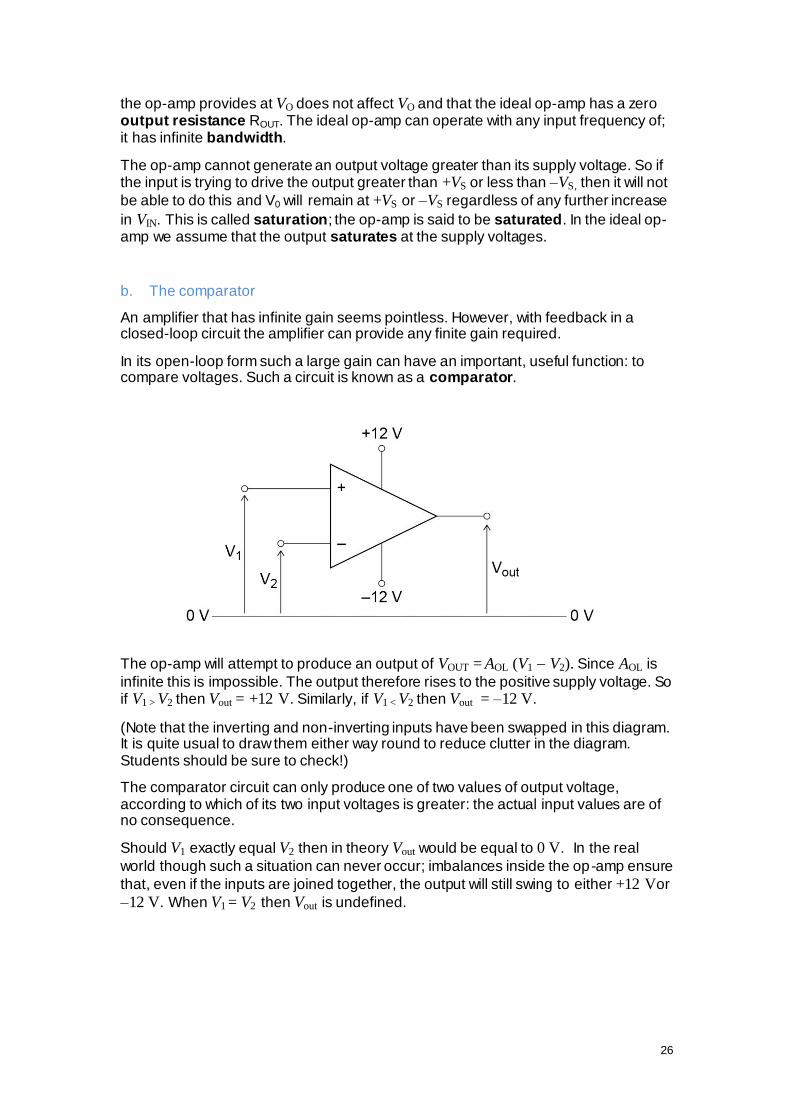
b. The comparator
An amplifier that has infinite gain seems pointless. However, with feedback in a closed-loop circuit the amplifier can provide any finite gain required.
In its open-loop form such a large gain can have an important, useful function: to compare voltages. Such a circuit is known as a comparator.
The op-amp will attempt to produce an output of VOUT = AOL (V1 V2). Since AOL is
infinite this is impossible. The output therefore rises to the positive supply voltage. So if V1 > V2 then Vout = +12 V. Similarly, if V1 < V2 then Vout = –12 V.
(Note that the inverting and non-inverting inputs have been swapped in this diagram. It is quite usual to draw them either way round to reduce clutter in the diagram. Students should be sure to check!)
The comparator circuit can only produce one of two values of output voltage, according to which of its two input voltages is greater: the actual input values are of no consequence.
Should V1 exactly equal V2 then in theory Vout would be equal to 0 V. In the real
world though such a situation can never occur; imbalances inside the op-amp ensure
that, even if the inputs are joined together, the output will still swing to either +12 Vor
–12 V. When V1 = V2 then Vout is undefined.

27
A typical use of the comparator is in a simple temperature alarm circuit – in this case one that sounds a buzzer if the temperature inside a freezer rises too high. The circuit, which makes use of a thermistor, is shown below.
The resistance of a thermistor changes with temperature. On the circuit diagram the thermistor resistance is indicated by RTH. The label –t°, together with the line through the symbol, indicate that this is a negative temperature coefficient device –its
resistance falls as its temperature rises. VR is a variable resistor and is used to set the temperature at which the buzzer will sound.
The potential divider formed by R2 and VR provides a fixed voltage V- to the
inverting input of the op-amp. The potential divider formed by R1 and RTH provides a
voltage V+ to the non-inverting input. This voltage is not fixed – it changes as the
temperature changes because RTH changes.
When the temperature is low RTH will be high, perhaps around MΩ. The voltage V+
will therefore be very low. Provided VR is set to ensure that V- is greater than this,
then the op-amp output, VOUT, will be at 0 V and the buzzer will be off. As the
temperature rises RTH falls, and V+ rises. At the point where V+ exceeds V- the op-amp output swings to the positive rail voltage and the buzzer turns on. By adjusting VR, and thus V-, the temperature at which this happens can be set.
A useful exercise is to swap either or both of the resistors and thermistor round, and then ask the students to explain the new circuit behaviour and its possible use.
The thermistor can be replaced with any other resistive sensor, such as an LDR with a similar behaviour.

28
Chapter 4 Operational amplifier circuits
There are four principle closed-loop circuit configurations for the op-amp which students need to understand.
A. The inverting amplifier
The inverting amplifier is one of the most common op-amp circuits.
(Notice that the power supply connections to the op-amp are not shown. This is usual practice; unless there is something special about them in a particular circuit they are assumed to be present.)
RF provides feedback to the circuit: the op-amp is thus operating in closed loop. Because the output is fed back to the inverting input, the circuit has negative feedback.
Because of its comparative simplicity, and because it is an extremely good vehicle for understanding how the op-amp works in closed-loop, students are required to be
able to derive the transfer function (ie how VOUT relates to VIN) for the inverting amplifier circuit.
Students are required to be able to derive the transfer function (ie, how VOUT relates
to VIN) for the inverting amplifier circuit. In the analysis of this, and the op-amp
circuits following, the op-amp is treated as ideal, and un-saturated (|VOUT| < VS).
The first step in the analysis is to label the circuit to show all currents and voltages.
Since VOUT is some value between ±VS, and since the op-amp amplifies the voltage
difference Vdiff between its inputs, then this difference must be Vdiff =
= 0 V
(To see this, for a real op-amp, the TL081 with its gain of 200 000, and an output of
5 V: Vdiff =
=
= 2 μV. This is so small compared with the other
voltages in the circuit that it can be assumed, for the purposes of deriving the transfer function, to be zero!)

29
Since the non-inverting input voltage is 0 V, then the inverting input voltage will also
be (approximately) 0 V. We call this point in the circuit, * on the diagram, a virtual earth, and the following is called a virtual earth analysis.
This derivation is laid out below in small, separate steps, in a particular order. Any correct, clearly presented, logical approach is acceptable from students when asked to reproduce this analysis.
(i) Since Vdiff V, then VR1 = VIN
(ii)
(iii) By Kirchoff’s current law at the virtual earth point (the vector sum of all currents at a node = 0): IR1 = Iin + IRF
(iv) Because Rin for the op-amp = ∞ then Iin = 0
(v) So, IRF = IR1
(vi)
(vii)
(viii) By Kirchoff’s voltage law (all voltages around a closed loop must sum to zero),
VOUT = VRF, so
(ix) (
)
(x)
-
An alternative way of looking at step (viii) is to say that since the left -hand end of RF is connected to the virtual earth, ie is at 0 V, then for VRF to be as shown the right-
hand end, ie at VOUT, must be at –VRF.
It is clear from the equation why this op-amp circuit is called an inverting amplifier. The diagram gives an example of this circuit in action.

30
B. The summing amplifier
A useful extension of the inverting amplifier is the summing amplifier. The virtual earth allows multiple signals to be connected to the inverting amplifier without mutual interference, each one being amplified independently. The output equals the sum of the individual input signals. The circuit, and its transfer function, are shown here:
– (
2
2
3
3
)
A common use for such a circuit is as an audio mixer. Different audio inputs eg CD player, MP3 player, PC etc. can be combined and their individual levels and the overall level can be adjusted.
C. The non-inverting amplifier
The inversion of an audio signal does not affect the sound. However, for some applications, the signal must retain its original polarity. The non-inverting amplifier achieves this by applying the signal to the non-inverting input. The feedback has to remain as before so that negative feedback is achieved. The circuit is shown below.
There is no virtual earth in this circuit, so the analysis is more difficult. (Students are
not required to reproduce this.) The transfer function is (
). It is
important to note that the gain can never be less than 1.
A significant difference (and advantage) between this circuit and the inverting amplifier is its input resistance. This is the resistance seen by any circuit connected
to it. Here, the input signal is connected to the non-inverting input. It thus ‘sees’ Rin for the op-amp which is infinite for an ideal device. This circuit therefore draws no current from the input signal. When students compare this with the inverting amplifier
circuit they should see that in this case the input resistance is equal to R1, the input resistor.

31
Looking at the equation shows that if RF is made zero, and/or R1 is made infinite, the
gain will be 1. The circuit then becomes:
This unity-gain amplifier is called a voltage follower (because VOUT ‘follows’ VIN) or
buffer. A buffer is an interface between a signal source that cannot deliver any (or only a very small) current, and a circuit or device with a low input resistance. It is a useful and frequent op-amp circuit. Notice that all of the output is fed back to the
input - this circuit has 100% feedback.
D. The difference amplifier
The principle behaviour of the op-amp – that it amplifies the difference between its two input signals – is exploited in this final op-amp circuit, the difference amplifier.
The transfer function is ( 3
2) 2 – (
) . Usually the difference
amplifier should have equal gain for each signal. To achieve this R3 is made equal to
RF and R2 is made equal to R1. The equation then becomes
( 2 – )
The difference amplifier is used a great deal in instrumentation where small amplitude signals are processed. Its major advantage in these applications is in noise cancellation. Two examples illustrate this. (Students do not need to study these. Questions on the difference amplifier will introduce and explain the context.)

32
a. The balanced microphone
In recording studios, microphone leads can often be long. The cables pick up noise and interference, the most significant of these usually being a 50 Hz signal from the
electrical mains. Filtering the 50 Hz signal out is not satisfactory, because there will be signals at this frequency in the audio and these would be lost. Instead, the microphone signal is converted into two signals, one normal, the other inverted, and this differential, or balanced signal is sent to the mixing suite.
On the way to the mixer the cable picks up hum; but because both signal cables are physically close to one another, the hum picked up by each cable is roughly identical. A difference amplifier then subtracts one signal from the other, and the hum is cancelled out.
(The signal from the microphone is shown here as being processed electronically to produce the balanced signals. This is not normally necessary because the physical construction of the microphone, with two sensing elements back-to-back, automatically produces a differential signal.)
b. The ECG amplifier
The electrocardiogram (ECG) is a time graph showing the electrical activity of the heart. The signals, usually less than 1 mV in amplitude, are picked up by placing a
pair of electrodes on the chest. The signal is then displayed on a screen or stored for later analysis.
The problem is that the human body is an effective aerial for electromagnetic
radiation, a big component of which is, again, the 50 Hz from the mains supply. A difference amplifier is used to eliminate the noise. This time the differential signal is achieved by placing a third electrode – the indifferent electrode – somewhere else on the body so that the noise signals picked up by each signal lead will be closely similar. Very often the indifferent electrode is placed on the wrist or the ankle. The indifferent electrode is the 0 V for the signal. Sometimes more than just three leads are used: the different signals have clinical significance.

33
E. Real operational amplifiers – their limitations
Hundreds of different op-amps are available. Although each one has its characteristics optimized for particular applications, the behaviour of the majority is close to ideal for most practical purposes. Almost anyone can be used as a ‘general purpose’ device.
One particular device needs a special mention. The 741 op-amp is an early device made by a large number of manufacturers. Its circuit has been revised many times over the years, but compared with modern op-amps it is far from ideal. It is quite easy to use it and to find that it does not perform as expected. So many better devices are available that teachers are advised not to use the 741 in the classroom.
There is inevitably a compromise between the key characteristics: for example, a large RIN can be at the expense of AOL; a large AOL can reduce the frequency
response. Fortunately amongst the thousands of types available it is possible to find an op-amp with optimal characteristics for any particular application.
Departures from the ideal
It is interesting to examine how the characteristics of a real device differ from of the ideal properties assumed in previous sections. The op-amp integrated circuit pictured is the Texas Instruments TL081. The key characteristics are shown in the table: full performance figures can be found in the manufacturer’s data sheet.

34
a. AOL
An open-loop gain of 200 000 is not large by modern op-amp standards: gains in
excess of 106 are not uncommon. However, even the TL081’s gain is high enough to
make the assumptions in the analyses hold very well.
b. Rin
The input resistance is extremely large – to all intents and purposes, infinite. This is achieved by having FETs in the input circuitry of the op-amp. This affects some of the
other parameters: it is the main reason, for example, why AOL is modest by modern op-amp standards.
c. Rout
Whilst other characteristics are impressive, Rout is rather high. There will be a limit to
the amount of current the op-amp can deliver. If it is part of a system where a loud speaker is to be driven, for example, then further power amplification will be needed. (As an aside, it is worth pointing out that one of the important effects of using the op-amp in a circuit with negative feedback is a reduction in Rout). Op-amps are not
generally used to drive large loads (although there are some that do), so this isn’t usually too much of a problem.
d. BW (bandwidth)
Because the op-amp has such a huge gain, changing its output signal from one power supply extreme to the other, say, cannot be done quickly (think of mechanical analogies with momentum and inertia). For this reason, the open-loop bandwidth of most op-amps is very small – typically 10–30 Hz. So where does the figure of 2.5
MHz for the TL081 come from?
What is quoted in the data sheets is not the open-loop bandwidth, but the closed-loop bandwidth, with the amplifier in a circuit where it has an overall gain o f unity. This figure is called the gain-bandwidth product, or GBP.
Characteristic TL081
AOL 200,000
Rin 1012 Ω
Rout 200 Ω
BW 2.5 MHz
Vout range to within 20% of each supply
35
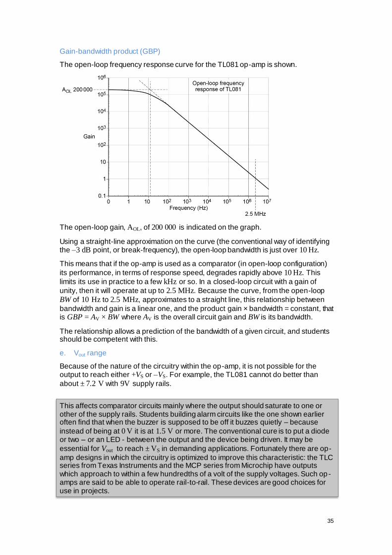
Gain-bandwidth product (GBP)
The open-loop frequency response curve for the TL081 op-amp is shown.
The open-loop gain, AOL, of 200 000 is indicated on the graph.
Using a straight-line approximation on the curve (the conventional way of identifying the –3 dB point, or break-frequency), the open-loop bandwidth is just over 10 Hz.
This means that if the op-amp is used as a comparator (in open-loop configuration)
its performance, in terms of response speed, degrades rapidly above 10 Hz. This
limits its use in practice to a few kHz or so. In a closed-loop circuit with a gain of
unity, then it will operate at up to 2.5 MHz. Because the curve, from the open-loop
BW of 10 Hz to 2.5 MHz, approximates to a straight line, this relationship between
bandwidth and gain is a linear one, and the product gain × bandwidth = constant, that is GBP = AV × BW where AV is the overall circuit gain and BW is its bandwidth.
The relationship allows a prediction of the bandwidth of a given circuit, and students should be competent with this.
e. Vout range
Because of the nature of the circuitry within the op-amp, it is not possible for the output to reach either +VS or –VS. For example, the TL081 cannot do better than
about ± 7.2 V with 9V supply rails.
This affects comparator circuits mainly where the output should saturate to one or other of the supply rails. Students building alarm circuits like the one shown earlier often find that when the buzzer is supposed to be off it buzzes quietly – because
instead of being at 0 V it is at 1.5 V or more. The conventional cure is to put a diode or two – or an LED - between the output and the device being driven. It may be
essential for Vout to reach ± VS in demanding applications. Fortunately there are op-
amp designs in which the circuitry is optimized to improve this characteristic: the TLC series from Texas Instruments and the MCP series from Microchip have outputs which approach to within a few hundredths of a volt of the supply voltages. Such op -amps are said to be able to operate rail-to-rail. These devices are good choices for use in projects.

36
Inside the op-amp
For interest, the circuit inside the TL081 op-amp is shown. There are 17 transistors (in this case MOSFETS) a typical value. Students are not expected to be able to reproduce this diagram.
Chapter 5 Digital signal processing
Digital signals were introduced in Chapter 2. Decision-making circuits, where a combination of digital input signals results in a particular output, are dealt with first followed by a group of circuits that process time-related digital signals as in clocks and counters.
A. Combinational logic circuits
A digital computer would seem the ideal candidate for accepting a number of digital signals and carrying out actions based on them. However, much decision making can be achieved using purpose-designed circuits containing logic gates. A good way to illustrate this and to introduce the different elements of such a circuit is to use the example of a power paper guillotine:
A motor drives a blade which cuts a stack of paper. The machine contains an interlock circuit so that the operators cannot damage their fingers. It also contains a paper stack height switch so that it cannot operate if too tall a stack of paper has been put in. The machine will only operate and drive the blade when a left-hand button is pressed, and a right-hand button is pressed, and the paper stack height switch is not operated.
Considering the buttons first, an output signal (to drive the blade motor) is required if, and only if, both of two input signals (from the buttons) are present. Such a device is called an AND gate, and its symbol is shown below.
The device gives an output of logic 1 when both inputs A and B are logic 1, otherwise logic 0 is shown. One convention is to have the input labels starting at the beginning of the alphabet and working forwards; output labels start at the end of the alphabet and working backwards. There is no accepted standard however.

37
The circuit for this part of the guillotine interlock system would then look like this:
The logic gate also has to have power supply connections of course but in practice they are assumed to be there and are not shown.
This circuit is not yet complete; the switch for the paper stack height logic is needed. Very often the design of a logic circuit can be achieved by careful inspection of the description of its intended operation. The output will operate if the left-hand button is pressed, and the right-hand button is pressed and the paper stack height switch is not operated. The clue is in the words!
What is needed to complete the circuit is a gate which produces an output of logic 1 if its input is logic 0, and vice-versa. This is called a NOT gate, and its symbol is shown below.
The circuit for the guillotine interlock can now be completed:
The combination of a number of different logic gates used together to make a decision is called a combinational logic circuit.
Describing the operation of such a simple circuit using words is easy. But in real, complex systems it quickly becomes impossible to do that. The behaviour of the logic circuit is then shown using a truth table. The table shows all the inputs, in all possible combinations, and all the resulting outputs.
38
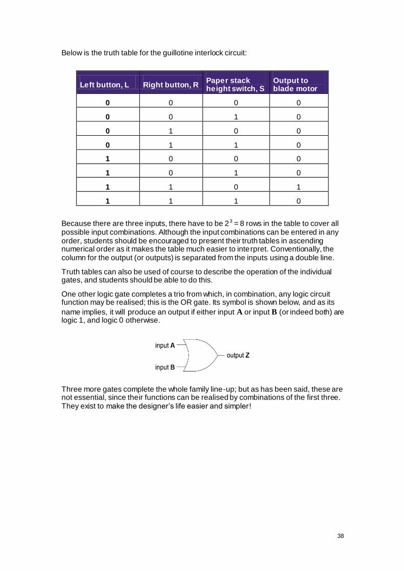
Below is the truth table for the guillotine interlock circuit:
Left button, L Right button, R Paper stack height switch, S
Output to blade motor
0 0 0 0
0 0 1 0
0 1 0 0
0 1 1 0
1 0 0 0
1 0 1 0
1 1 0 1
1 1 1 0
Because there are three inputs, there have to be 23 = 8 rows in the table to cover all possible input combinations. Although the input combinations can be entered in any order, students should be encouraged to present their truth tables in ascending numerical order as it makes the table much easier to interpret. Conventionally, the column for the output (or outputs) is separated from the inputs using a double line.
Truth tables can also be used of course to describe the operation of the individual gates, and students should be able to do this.
One other logic gate completes a trio from which, in combination, any logic circuit function may be realised; this is the OR gate. Its symbol is shown below, and as its
name implies, it will produce an output if either input A or input B (or indeed both) are logic 1, and logic 0 otherwise.
Three more gates complete the whole family line-up; but as has been said, these are not essential, since their functions can be realised by combinations of the first three. They exist to make the designer’s life easier and simpler !

39
They are shown below, together with their truth tables:
The EOR gate (Exclusive OR, also known as XOR gate, or EXOR gate) is a very useful function, and overcomes what is often in practice an unwanted characteristic of the OR gate, which gives a 1 output if both inputs are 1. The EOR gate is sometimes called a digital comparator or an inequality gate (because it gives an high output if its inputs are different). A useful exercise, to help embed knowledge of logic gates, is to invite students to design the EOR function using a combination of only AND, OR and NOT gates. One correct solution (not the simplest!) is below.
Logic gate devices in practice
Practical logic gates are not discrete electronic devices, but instead are integrated circuits constructed with transistor switches. Students are not required to study the internal construction of gates.

40
Power supplies for logic chips
In almost all logic gate chips the power supply is connected between pin 7 (0V) and
pin 14 (+V). Some logic chips are 16-pin types, in which case the pins at the corners
are still the relevant ones, ie pin 8 is 0V and pin 16 is +V.
For a long time, 5 V has been the standard choice for logic chip power supplies. This is because the first major ‘family’ of logic devices (TTL – Transistor-Transistor-Logic) could only work at this voltage. A common later family, CMOS (Complimentary Metal-
Oxide Semiconductor), will work at voltages up to 15 V or more, and is a much better
choice for experimental work because a 9 V battery can be used as the power
source. Modern logic systems and devices work at increasingly lower voltages, 3.7 V
being typical, and 5 V systems are still very common.
There is no reason for students to use anything other than CMOS logic devices; apart from the much wider power supply range they consume little or no power, and so are ideal for use in battery powered projects.
Designing and analysing logic circuits
Truth tables are a powerful tool when it comes to analysing a combinational logic circuit and to constructing a circuit from its truth table. Students should be competent at both.
However, when the logic system is complex, truth tables become unwieldy. Also, deriving a circuit from its truth table often leads to a need to simplify it using fewer gates. Boolean algebra is used for just this purpose; it provides a means of defining a circuit mathematically and then optimising it. Both techniques, which students must be able to use, are considered in more detail below.
Some of the examples here are more complex than required by the specification. Teachers need to be aware of this and should consult the specification when setting work for students.
a. Analysing a circuit with a truth table
The circuit below is of the EOR gate derived earlier.

41
Producing a truth table for a circuit like this is made much easier if intermediate signals are identified and labelled on the circuit. These are signals which are ‘internal’ to the circuit, ie are not system inputs or outputs. The circuit then becomes:
The truth table can then be constructed, including the intermediate signals, putting in all the input combinations and working out the signals from left to right.
b. Using Boolean algebra
Boolean algebra is an invaluable tool, not just in digital circuits but in logic, statistics and set theory. In Boolean algebra, logical relationships between variables (in our case, ‘signals’) are written thus:
( )
There are rules that enable combinations of the functions to be manipulated.
1. the associative law:
( ) ( )
( ) ( )
2. the commutative law:
3. the distributive law:
( ) ( ) ( )
( ) ( ) ( )

42
Next, by looking at A as the signal into one or both inputs of a logic gate, it is easy to establish the following simplifications:
Students should satisfy themselves that these laws and simplifications are true.
Finally, there is another law which is crucially important in the design and simplification of logic circuits. Knowledge or use of this law is not required in the
specification. This is De Morgan’s Law which states that
and
Armed with this arsenal of techniques, we can look at a logic circuit in Boolean terms and manipulate it.
Taking the EOR truth table from before and highlighting the inputs that produce an output of 1:
… and then writing its transfer function in Boolean form, we get:
( ) ( )
Inverting both sides gives:
( ) ( )
Applying De Morgan’s law:
( ) ( )
… and inverting again to get back to Z:
( ) ( )
On the face of it not a great deal has changed – the expression actually looks more complicated than before. However, inspection reveals that there is only one logic function in this expression – the NAND gate. The NAND gate is one of the simplest (and therefore cheapest) gates to fabricate. In large logic systems it also makes good economic sense to use as few different types of gate as possible. For this reason,
𝐀 𝐀 𝐀
𝐀 0
𝐀 𝐀 𝐀
𝐀 1
𝐀 0 0
𝐀 1 𝐀
𝐀 0 𝐀
𝐀 1 1
43
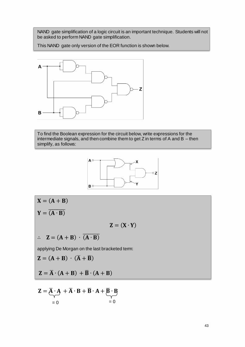
NAND gate simplification of a logic circuit is an important technique. Students will not be asked to perform NAND gate simplification.
This NAND gate only version of the EOR function is shown below.
To find the Boolean expression for the circuit below, write expressions for the intermediate signals, and then combine them to get Z in terms of A and B – then simplify, as follows:
( )
( )
( )
( ) ( )
applying De Morgan on the last bracketed term:
( ) ( )
( ) ( )
𝐙 𝐀 𝐁 𝐀 𝐁
= 0 = 0

44
hence:
… which is the Exclusive Or function again:
This can also be written using the accepted symbol for the EOR function, as:
Students should be given plenty of practice creating Boolean expressions from a
given circuit and/or truth table, manipulating them, and simplifying them using the
laws of Boolean algebra within the limits of the specification.
B. Sequential logic circuits
So far we have examined circuits with ‘static’ inputs – the inputs are presented to the circuit and an output based on the state of its inputs is generated. In many systems, however, we want to generate or process signals that are time-dependent, following a pre-defined sequence. Broad categories include timing, counting and sequencing circuits. Most systems of any complexity have some digital circuits of this type and they are known as sequential logic circuits. What follows gives examples of some of the most common and useful circuit elements of sequential logic.
A common signal in sequential logic systems is a pulse; this is a signal which turns on (or off) very briefly either in response to some event, or at regular time intervals. The last section of this chapter will look at the generation of regular streams of pulses.
Students are only expected to treat the logic circuits as functional ‘blocks’. The details of the circuitry within each block that creates the overall function should not need to be considered. However some insight into this is given for interest.
Simple logic gate chips are classed as SSI – Small Scale Integration, because they do not contain very many devices. The chips we are now going to consider are MSI (Medium Scale Integration) or even LSI (Large Scale Integration) chips.
a. Counting circuits
Counting logic signals is a fundamental requirement in many systems. For instance, digital watches count one-second timing pulses, work out the total number of seconds, minutes and hours, and then display the result on an LCD screen. Counting chips always count in binary; but they may present the results of the counting process – the outputs of the chip - in other forms.
The generalized N-bit counter chip is shown below:
45
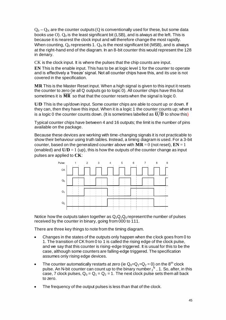
Q0 – QN are the counter outputs (Q is conventionally used for these, but some data
books use O). Q0 is the least significant bit (LSB), and is always at the left. This is because it is nearest the clock input and will therefore change the most rapidly.
When counting, Q0 represents 1. QN is the most significant bit (MSB), and is always
at the right-hand end of the diagram. In an 8-bit counter this would represent the 128 in denary.
CK is the clock input. It is where the pulses that the chip counts are input.
EN This is the enable input. This has to be at logic level 1 for the counter to operate and is effectively a ‘freeze’ signal. Not all counter chips have this, and its use is not covered in the specification.
MR This is the Master Reset input. When a high signal is given to this input it resets the counter to zero (ie all Q outputs go to logic 0). All counter chips have this but
sometimes it is so that that the counter resets when the signal is logic 0.
U/D This is the up/down input. Some counter chips are able to count up or down. If they can, then they have this input. When it is a logic 1 the counter counts up; when it
is a logic 0 the counter counts down. (It is sometimes labelled as to show this)
Typical counter chips have between 4 and 16 outputs; the limit is the number of pins available on the package.
Because these devices are working with time-changing signals it is not practicable to show their behaviour using truth tables. Instead, a timing diagram is used. For a 3-bit
counter, based on the generalized counter above with MR = 0 (not reset), EN = 1
(enabled) and U/D = 1 (up), this is how the outputs of the counter change as input
pulses are applied to CK:
Notice how the outputs taken together as Q2Q1Q0 represent the number of pulses received by the counter in binary, going from 000 to 111.
There are three key things to note from the timing diagram.
Changes in the states of the outputs only happen when the clock goes from 0 to 1. The transition of CK from 0 to 1 is called the rising edge of the clock pulse, and we say that this counter is rising-edge triggered. It is usual for this to be the case, although some counters are falling-edge triggered. The specification assumes only rising edge devices.
The counter automatically restarts at zero (ie Q0=Q1=Q2 = 0) on the 8th clock pulse. An N-bit counter can count up to the binary number 2
N – 1. So, after, in this case, 7 clock pulses, Q0 = Q1 = Q2 = 1. The next clock pulse sets them all back to zero.
The frequency of the output pulses is less than that of the clock.

46
In fact, the frequency (or, more precisely the ‘pulse rate’ – see later) is ½ the clock for Q0, ¼ for Q1 and 1/8th for Q2. This makes the counter useful as a frequency divider. Typically a digital watch contains a circuit producing pulses at a precise rate of 32,768 Hz. A frequency divider generates 1-second pulses for the clock itself. Students can decide the number of stages required in order to achieve this.
The modulo-n counter
There are many systems in which counters are required whose terminal count is not a power of 2 but some other number. For example, a counter may be used in a digital clock to count the seconds. This counter must count to 59 and then return to zero on the 60th pulse; a 6-bit counter would reset on the 64th pulse, and a 5-bit on the 32nd.
A counter can be forced to reset at any number within its range by making use of the MR (reset) input, and possibly some logic gates.
Using the example of the 60-second counter, the following circuit will achieve this behaviour.
The EN and U/D inputs are connected to the supply, so that they are held at logic 1.
The first time from zero that outputs Q2 (=4 s), Q3 (=8 s), Q4 (=16 s) and Q5 (=32 s) are all at logic 1 is at a count of 60 (4+8+16+32). The AND gate circuit then produces an output of 1 which resets the counter to zero. When a counter is used like this it is called a modulo-n counter. This example is modulo 60 and this is a method that can be used to produce a counter counting to any integer.
The BCD counter
A particular type of modulo-n counter is the Binary-Coded-Decimal, or BCD, counter.
In order to drive the digits of a multi-digit decimal display (eg for a timer, or a voltmeter), a binary pattern representing the numbers 0–9 is required for each digit.
This can be achieved with a 4-bit binary counter chip (which counts up to 15) and logic to create a modulo-10 counter. This is such a common requirement that manufacturers designed a range of counter chips which have the necessary logic circuit built-in. Although the output is in binary form, it only ever counts from 0 to 9 – hence the rather misleading ‘BCD’ name. Such counters are very similar in all respects to regular counters, but they usually also have an additional output called CO (carry-out). This enables several chips to be daisy-chained for multi-digit displays.
This is how it works. The CO output is normally high. It then goes low when its counter reaches a count of 9, and then back high when it reaches a count of 10 (and resets). The CO signal is connected to the CK (clock) input of the next counter along.

47
By this means a multi-digit decimal counter is achieved. This is shown in the diagram below.
The Johnson counter
The last type of counter to look at is a very useful device, which doesn’t present its outputs in binary form. It has ten outputs, which turn on in sequence as clock pulses are received. In this respect it is much more like a decimal counter than the BCD counter is; it is sometimes called a decade counter for this reason.
The diagram below shows the Johnson counter layout, and below that its timing diagram.
Notice that the Q0 output represents zero, and hence is high when the counter is reset.

48
A very common use for the Johnson counter is as a sequencer. In devices or systems where a number of operations have to be carried out one after the other, each lasting for a given period of time, it can be used to provide the contro l signals for these operations. For example, in a washing machine part of its washing cycle may involve: rotating the tub for 3 seconds pausing for 2 seconds heating for 4 seconds; then repeating. This could be achieved with a Johnson counter as in the diagram below.
C. Astables
Counters count the number of pulses fed to them – but how are these pulses produced in the first place? To count the number of people who have entered a building, pulses will be produced by a detector in the doorway. But in many systems, for example the washing machine sequencer above, what is needed is a regular train of pulses that form the timebase or clock for the whole operation. This section introduces the idea of the pulse generator and shows some of the principles behind its operation.
Pulse generators (sometimes called ‘continuous pulse producers’) are usually based around a class of circuits called astables. Astable means not having any stable states – a circuit that turns on and off continuously, not being able to rest in either state. Astable circuits can be made with discrete components ie transistors, diodes and passive components but this is rarely economical because astable chips are readily available and because it is easy to construct an astable using logic gates.
This section treats the astable as a block. One particular chip has been the staple diet of electronic circuit designers (professional and amateur) for many decades – the 555. Although old, it is still a useful chip – though its use by the commercial world is declining as there are now many more sophisticated and convenient alternatives.
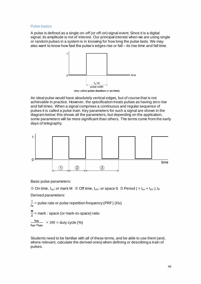
49
Pulse basics
A pulse is defined as a single on-off (or off-on) signal event. Since it is a digital signal, its amplitude is not of interest. Our principal interest when we are using single or random pulses in a system is in knowing for how long the pulse lasts. We may also want to know how fast the pulse’s edges rise or fall – its rise time and fall time.
An ideal pulse would have absolutely vertical edges, but of course that is not achievable in practice. However, the specification treats pulses as having zero rise and fall times. When a signal comprises a continuous and regular sequence of pulses it is called a pulse train. Key parameters for such a signal are shown in the diagram below: this shows all the parameters, but depending on the application, some parameters will be more significant than others. The terms come from the early days of telegraphy.
Basic pulse parameters:
On time, ton; or mark M Off time, tof f ; or space S Period ( = ton + tof f ), tP
Derived parameters:
= pulse rate or pulse repetition frequency (PRF) (Hz)
= mark : space (or mark-to-space) ratio
× 100 = duty cycle (%)
Students need to be familiar with all of these terms, and be able to use them (and, where relevant, calculate the derived ones) when defining or describing a train of pulses.

50
Generating pulses with an astable
The basis of nearly all timing circuits or systems in electronics is the RC circuit.
Wherever there are pulses, delays, or tones, they will usually be provided by an RC
circuit. The charge and discharge of RC networks is covered in the core specification.
Astable circuits exploit RC charging behaviour and together with switching circuits
generate a single pulse or pulse train. Circuit details do not need to be understood, but basic ideas are important. The generalized astable is:
The NOT gate (or inverting switch circuit) has hysteresis (the special symbol for hysteresis is shown in the block). This means that it has two different switching thresholds – an upper and a lower, and this is an essential feature of any astable circuit. This idea was met in Chapter 2 with the Schmitt trigger, and this device is an ideal candidate here.
In operation the astable works as follows.
Initially, C is discharged, so the input to the NOT gate is 0. Its output is thus at
logic 1, and so C starts to charge via R.
When the voltage on C reaches the upper switching threshold, the NOT gate
recognizes its input as a logic 1, so its output switches to 0. C therefore starts
to discharge through R.
When the voltage on C has dropped to the lower switching threshold, the NOT
gate recognizes its input as a logic 0 again, so its output switches to 1. C therefore starts to charge again.
The whole process repeats indefinitely, producing a train of on-off pulses at the output.
Because C both charges and discharges through the same resistor, the on and off times (ton and toff) will be identical. With a slightly more complicated switching
arrangement they can be made different and independent of each other.

51
A NOT gate with hysteresis typically has a lower switching threshold of close to
(
). Using these values the general
shape of the voltage across the capacitor VC,and the output voltage are as shown on the following diagram.
Notice that the initial pulse width is wider than any of the successive ones. This is characteristic of the astable and occurs because at initial switch-on the capacitor is
completely discharged, whereas once the astable is functioning C never completely
discharges, and starts charging again from
.
Using the equation for the voltage across a capacitor in an RC charging circuit
(3.7.3.4) it is possible to work out what the pulse rate of the astable will be, and it can be seen that this is dependent on the magnitude of the two thresholds. In this case,
ton is the time taken for VC to rise from
. Similarly, toff is the time taken to
fall from
. Since these two are the same, it is only necessary to calculate
one of them to find the period (ton + toff) and hence the pulse rate.
For a charging capacitor ( – –
). Since Q = CV, and V0 = VS, the supply
voltage, then ( – –
). From the graph it can be deduced that the on-time,
ton is the time it takes VC to rise from zero to
. Calling these two times t1 and t2
respectively, we have
V
( – –
) –
33. Taking natural logarithms gives
–
33 from which we get: t1 = 1.11RC. A similar process for t2 yields
t2 = 0.41RC. ton is thus 1.11RC – 0.41RC = 0.7RC. Notice that this is very close to
0.69RC, the time constant of the circuit. In fact, for these particular switching
thresholds this is generally taken to be the case. Thus the period tP (= ton × 2) is
1.4RC and the pulse rate, or pulse repetition frequency (PRF) is
.
Students will not be asked to manipulate the charging equation like this. However, they will be expected to understand the principle, and may be given a question which involves the estimation of the PRF, given the switching thresholds.

52
Chapter 6 Data communication systems
This chapter looks at the principles of communications systems (section 3.13.6), which these various technologies and techniques share; the way in which data have to be prepared for transmission; the different media that carry data; data encoding, and the bandwidth needed by a communications channel.
A. Principles of Data communication systems
The generalised communications system is shown below.
a. Input transducer
This converts the source of information (or data) into an electrical signal for the system. Typically this could be a microphone, a computer, a television camera, etc.
b. Modulator
The modulator processes the signal to make it suitable for the transmission path. Thus for a radio wave link, a radio wave must be provided to carry the data.
c. Transmitter amplifier
An amplifier then boosts the signal to an appropriate level to send over the transmission link.
d. Transmitting device
This converts and sends the prepared electrical signal into a suitable form for the transmission path. For a radio link this would be an aerial. For an optical system it would probably be a laser diode or infrared LED.
e. Transmission path
This is the medium through which the signal is sent. For a radio wave link this would be free space; for an optical link it would be an optical fibre, etc. Simple communications systems might have a copper cable as the medium.
f. Receiving device
This receives and converts the signal back into an electrical signal for the rest of the system. In a radio link this would be another aerial; in an optical link it would probably be a photodiode.

53
g. Receiver amplifier
Usually the information signal has travelled some distance and is weakened. This boosts it to a level for subsequent processing.
h. Demodulator (sometimes called ‘Detector’)
The function of the demodulator is to obtain the original signal in an appropriate form.
i. Output amplifier
This boosts the recovered information signal to a level suitable for driving an output transducer, for example, a loudspeaker for a radio
j. Output transducer
This converts the signal into a form suitable for the purpose. For example, an electric motor for a garage door opening system.
Students do not need to know how each of the subsystems actually functions or the circuitry that might be involved. They will be expected to be able to explain the purpose of each subsystem and to be able to reproduce all or parts of the generalised communications system diagram.
B. Transmission media
The chosen data path depends on a number of factors. The three main media used are listed below, together with an overview of their advantages, disadvantages and characteristics. Students should know and be able to discuss the merits and characteristics of each, and to understand in broad terms how they are used. Students must know the approximate frequency bands applicable to each medium.
1. Copper cable
This is a common medium for short distances and relatively low data rates.
Transmitter and receiver are linked by a direct electrical wire connection. This direct linkage is a disadvantage of this medium.
Within this category there are three main types.
i. Coaxial cable
Mainly used for radio, television or other high frequency signals, not suitable for long distances. Typically found in homes, connecting the TV aerial or satellite dish to the television.

54
Consists of an insulated central copper conductor, completely enclosed in a copper sheath (or screen). The copper sheath is the 0 V connection, and provides electrostatic shielding, giving the cable some immunity from outside interference.
Not especially expensive, but has a practical upper frequency limit of around 1 GHz or so. At which it has an attenuation (signal loss) of typically 0.6 dB m-1, meaning that the signal power halves about every 5 m.
Not very secure.
ii. Twisted-pair cable
Used almost exclusively for computer networking.
Several sets of pairs of conductors are twisted together, giving each pair good noise immunity. Signals sent differentially down the wires, improving the noise immunity of the system.
Upper frequency limit of about 100-250 MHz. For a length of 100 m at 100 MHz the attenuation is typically 24 dB. The signal power thus halves approximately every 12 ½ m – over; twice as good as coaxial cable.
Cheap medium, an advantage for commercial use. Slightly more secure than coaxial cable but can still be tapped into.
iii. Plain copper wire
Ordinary wire or cable. Poor noise immunity.
Radiates energy easily, so unsuitable for high frequencies. It is also very insecure.
Low cost compared with other solutions.

55
2. Optical fibre
Transmission media of choice for non free-space communications links, because it has a large bandwidth.
A disadvantage that it ties the transmitter and receiver together; but it has many advantages that more than compensate for this.
The principle of operation is to send pulses of light down a very thin glass fibre
(between 8– μm diameter, depending on the type – see later).
The rays of light travel down the fibre in one of two operating modes (see later) to emerge at the other end of the fibre. Very high signal frequencies are achievable, so that many data channels can use a single fibre. Equally, the small size of each fibre means that hundreds of individual and independent fibres can be included in one ‘cable’.
It is commonly used for telephone systems to transmit thousands of simultaneous conversations down one bundle of fibres, and to deliver broadband services. Data
rates of up to 270 Gbps (270 × 109 bits/second) have been achieved in a single fibre.
As the light is confined to the fibre, it is almost totally immune to noise, and there is no interference between adjacent fibres.
Optical fibres are also very secure; it is impossible to tap into a fibre without breaking into the fibre. This would then require optical termination of the broken ends.

56
There are two main types of optical fibre available; multi-mode and single-mode (or mono-mode).
Single -mode is now the most commonly used because it is smaller and has improved characteristics.
The principles of optical fibres is covered in the core specification (3.3.2.3), but some is repeated here for convenience.
Multi-mode fibre
This type of optical fibre relies on total internal reflection (TIR) for its operation: a diagram showing the principle of operation is overleaf.
It is also called step index fibre because of the refractive index ‘step’ between the core and the cladding.
As with all media, the signal is attenuated the further it travels. However, the attenuation is much less than copper cable at about 3 dB km
-1 (ie the light has half
the original power after 1 km).
An important problem is that the light source will have a certain beam width, and will launch rays into the fibre with a range of trajectories. The path taken through the fibre will therefore be different depending on the initial direction of the light ray. This can cause problems because different ray paths will result in different travelling distances and rays will at the receiving end ‘out of sync’ with each other. This effect is called dispersion. This lengthens a pulse in distance, and therefore in time – the pulse becomes ‘smeared’ as well as attenuated:
Eventually this prevents individual pulses from being distinguished.

57
Mono-mode (or single-mode) fibre
A common and effective way of avoiding or minimizing dispersion is to make the fibre much narrower, to reduce the number of possible paths. Fibre diameters of 8 μm are comparable to the wavelength of the rays themselves, which as a result then propagate down the fibre in the same way that an electromagnetic wave propagates down a metal waveguide (a precisely dimensioned metal tube down which a high-frequency electromagnetic wave will propagate with very low loss - not required in this Option). The light then propagates in ways other than by TIR. Such fibres are called mono-mode, or single-mode fibres and are more difficult – and therefore more expensive – to make than multi-mode. They attenuate much less than multi-mode
fibres - typically the loss is about 0.5 dB km-1
.
The diagram below shows the principle difference between the operating characteristics of the two types.
3. Electromagnetic waves in free space
Here there is no physical link between transmitter and receiver, and this can be its main rationale (for example, wireless keyboards and mice for computers). Data are sent from transmitter to receiver via an electromagnetic wave in free space.
Electromagnetic waves are by their nature very easy to intercept making the method potentially insecure. In practice this may not be a problem: the main consumer radio and TV broadcasts do not need security; and data can be encrypted using very sophisticated methods. Wireless transmission can be a cheap way to send information over long distances, but can also be expensive – for example if the communication link involves the use of satellites.
Students should be familiar with the electromagnetic spectrum both in terms of labels and frequencies. The region of the spectrum used for data transmission is from
longwave radio waves (at about 60 kHz) up to microwaves (at about 100 GHz).
These are essentially practical limits. Aerials needed to transmit and receive waves below 60 kHz are prohibitively large (the dimensions of an efficient aerial have to be
comparable to about ½ the wavelength). Above 100 GHz wavelengths are small and the receivers are difficult and expensive to fabricate.

58
i. Longwave
Longwave (LW) wavelengths extend from about 2 km to 1 km (frequencies of about
150 kHz–300 kHz). The BBC broadcast radio on this frequency band for many years
(Radio 4 still uses it in addition to its VHF transmission). It is also used to broadcast the National Physical Laboratory’s 60 kHz MSF signal, an accurate time signal based
on a caesium clock that is used by radio controlled clocks and watches.
One huge advantage of longwave signals is the long distance they will travel. This is because, due to their long wavelength, they are more easily diffracted around obstacles, including the Earth’s surface. Further, the differing refractive indices of the atmosphere and the Earth mean that they can propagate as ground waves (or surface waves), covering huge distances. So electromagnetic waves do not necessarily travel in straight lines, avoiding the problem that transmitter and receiver need to be in line of sight.
ii. Shortwave
Shortwave (SW) covers wavelengths from about 100 m – 10 m (frequencies of about
3 MHz–30 MHz) and is used to broadcast consumer programmes, long-distance
communication to ships and aircraft, and to remote areas. It is also the main frequency band used by amateur radio enthusiasts (radio ‘hams’).
These uses stem from the fact that, like longwave, shortwave also propagates over vast distances; but by a different phenomenon – sky wave. Over a certain range of
frequencies (above about 500 kHz), the ionosphere reflects radio waves, and they
return to Earth. Thus they can be received beyond the horizon.
iii. Microwaves
Wavelengths between about 3 mm–150 mm (frequencies about 100 GHz–2 GHz) are called microwaves, and, apart from their use in microwave ovens, are important for communication. The 3G mobile phone network uses microwaves, as do satellite
systems, and Bluetooth® – which uses the 2.4 GHz band. Such systems need line-of-sight between transmitter and receiver; effective diffraction does not occur at such high frequencies. Aerials are also more complex than at lower frequencies involving waveguides, ‘dish’ aerials, or resonant cavities. These are metal boxes of precise dimensions, into which the microwave signal is launched, and within which resonance can occur (the cooking compartment of a microwave oven is an example of such a cavity).

59
iv. Telemetry
A narrow range of frequencies centred around approximately 433 MHz and 866 MHz, is used for telemetry.
Telemetry (which uses other frequencies too) is the control and monitoring of, and data capture from remote equipment. Remote-control garage doors and river monitoring for flood warning systems are examples of both uses.
See the resources guide for a range of fairly cheap telemetry modules, which can be used to demonstrate radio communication principles.
Summary
The table summarizes the characteristics of each of the main media above, in terms of security, cost, ease of use and bandwidth (transmission rates).
Students should be able to highlight major and important differences, and to give a reasoned argument for the choice of method in a given situation.
Medium Security Ease of Use Cost Bandwidth
Copper cable
Low.
Easy to install and use but can be very bulky. Ties transmitter to receiver.
Medium to very high: a long run of very large capacity copper cable can be very pricey.
Low to medium.
Optical fibre
Very high.
Fairly easy to use, but needs special terminations. Lightweight. Ties transmitter to receiver.
Multi-mode low; mono-mode fairly high.
Extremely high.
EM waves in free space
Intrinsically low, but data coding makes high.
Easy; but at high frequencies line-of-sight only, so needs repeaters.
Installation cheap because no physical link between TX and RX. But equipment at either end can be expensive.
Very high overall, but licencing arrangements restrict the bandwidth for individual users.

60
Satellite systems
An overview of communication systems would be incomplete without a description of satellite communications. Artificial satellites are launched into space, to provide telecommunications between points on Earth. The satellite receives signals from Earth and re-transmits them, achieving long distance communications links.
Satellites operate in two main different orbits: low Earth orbit lower Earth orbit (LEO) and geostationary orbit (GEO). LEO satellites are positioned at an altitude between
160 km and 1600 km (100 and 1000 miles) above Earth. GEO satellites are
positioned 35 786 km (22 236 miles) above Earth, completing one orbit every day
and thus remaining over one fixed spot on the Earth (specification 3.7.1.4).
Non-geostationary satellites have to be tracked and are only ‘visible’ from one
location for part of each 24 hour period. This makes them unsuitable for some purposes. But they are comparatively cheap to launch and to maintain.
The transmission path from Earth to satellite is called the up-link, and the return path the down-link. The signal travels long distances and the satellites have only a modest amount of electrical power, so the down-link signals received require much amplification. The up-link transmission frequency must be different from the down-link frequency. This prevents the high-power down-link signal from the satellite from overwhelming the weak up-link signal (as received at the satellite). This would de-sensitise the high-gain up-link receiver.
Satellites operate in the microwave region. Eg the BBC television service uses the Astra 2E and HOTBIRD satellites, down-link frequencies between 10–11 GHz. The
Aura satellite, used for climate research, operates at around 2.3 GHz. The Earth Resources Observation Satellite (EROS) is a series of commercial observation
satellites operating at around 8 GHz.
C. Multiplexing
Data transmission rates in a system can be dramatically increased if the transmission path is shared by a number of different data streams (for example, many telephone calls down one optical fibre). There are two main ways of doing this: time-division multiplexing (TDM) and frequency-division multiplexing (FDM).
Time-division multiplexing (TDM)
The idea behind TDM is to share the time between multiple data streams by allocating a defined time slot (‘time slice’) to each.
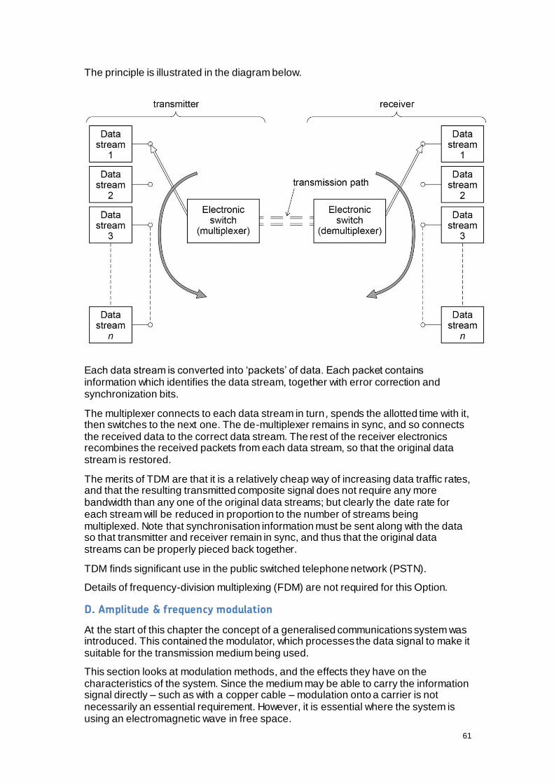
61
The principle is illustrated in the diagram below.
Each data stream is converted into ‘packets’ of data. Each packet contains information which identifies the data stream, together with error correction and synchronization bits.
The multiplexer connects to each data stream in turn, spends the allotted time with it, then switches to the next one. The de-multiplexer remains in sync, and so connects the received data to the correct data stream. The rest of the receiver electronics recombines the received packets from each data stream, so that the original data stream is restored.
The merits of TDM are that it is a relatively cheap way of increasing data traffic rates, and that the resulting transmitted composite signal does not require any more bandwidth than any one of the original data streams; but clearly the date rate for each stream will be reduced in proportion to the number of streams being multiplexed. Note that synchronisation information must be sent along with the data so that transmitter and receiver remain in sync, and thus that the original data streams can be properly pieced back together.
TDM finds significant use in the public switched telephone network (PSTN).
Details of frequency-division multiplexing (FDM) are not required for this Option.
D. Amplitude & frequency modulation
At the start of this chapter the concept of a generalised communications system was introduced. This contained the modulator, which processes the data signal to make it suitable for the transmission medium being used.
This section looks at modulation methods, and the effects they have on the characteristics of the system. Since the medium may be able to carry the information signal directly – such as with a copper cable – modulation onto a carrier is not necessarily an essential requirement. However, it is essential where the system is using an electromagnetic wave in free space.

62
Aerials have to be of the order of ¼ to 1 wavelength to enable an electromagnetic wave to propagate. At 60 kHz – the lowest frequency used for normal radio
communication, the wavelength is about 5 km. This makes the process at lower frequencies totally impracticable. To be able to send a low frequency information signal (eg music, where the frequency range is 25 – 20 000 Hz) therefore, the information or data signal is ‘translated’ to a wave with a much higher frequency which can then propagate with a sensible sized aerial. The modulator achieves this.
There are two main ways of doing this – Amplitude Modulation, or AM and Frequency Modulation, or FM.
Amplitude modulation (AM)
In AM, the amplitude of the information signal controls the amplitude of a high frequency signal called the carrier.
In block diagram form the process is as shown:
Here, the information signal is assumed to be a sine wave; but it could equally be a digital signal.
The waveform of the modulated signal is shown below. The left-hand one is for a sine-wave information signal, the one on the right for a digital signal.
The information signal becomes the envelope of the carrier signal.

63
The frequency spectrum of the modulated signal shows that the composite wave is at a high frequency. A modulated sine wave produces a simple spectrum and is used for the graph (students will not need to know the spectrum for a digital signal).
The process of modulation produces two additional frequencies, fL and fU. These are
called the side frequencies, and they are equal to the sum and difference of the frequency of the carrier, fC and of the information signal fm, ie
m
m
So, if the information signal is a sine wave with a frequency of 1 kHz, and the carrier
is 100 kHz, the two transmitted side frequencies will be 99 kHz and 101 kHz.
What about real signals? Although the range of human hearing is taken to extend to 20 kHz, there is simply not enough space in the AM radio spectrum to allow a bandwidth of 40 kHz for each station. For this reason, speech and music on the AM
radio band have their frequency ranges limited to about 4 kHz.
Radio 5 Live broadcasts with a carrier frequency of 909 kHz, AM modulated. So
there will be a whole range of side frequencies, varying in amplitude from moment to moment and covering the frequency range 905 kHz to 913 kHz. Side frequencies
then become sidebands, and the frequency spectrum graph becomes:

64
Clearly indicated on the spectrum plot is the frequency ‘space’ required for the composite signal, ie its bandwidth. It is:
Bandwidth of an AM signal: 2 m
(Hz) where fm is the maximum frequency
present in the information signal. Thus, AM transmitters cannot use carrier
frequencies that differ by less than 8 kHz (= 2 4 kHz). In practice, the spacing is 9 kHz to ensure that there is no adjacent channel interference.
Frequency modulation (FM)
In FM, the amplitude of the information signal controls the frequency of the carrier. This has a number of advantages over AM, but these come at a price. AM modulation and demodulation processes are very straightforward, but in FM they are more complex. FM also potentially requires greater bandwidth.
The waveform of the FM modulated signal is shown in the graph below. This again uses a sine wave as the information signal.
Note that the amplitude of the modulated signal remains constant.
Plotting the spectrum of an FM signal yields a very different picture from AM. For FM, the side frequencies extend to infinity in both directions. The significant part of the
spectrum plot for a sine wave information signal of frequency fm might look like the picture below.

65
However, whilst the mathematics of FM predicts frequency components at
fc ± integer multiples of fm
as shown on the graph, the relative amplitudes of these components can be very different to those shown, and indeed in some cases the carrier component even disappears. The explanation is that the exact shape of the spectrum depends on another factor – the frequency deviation.
The amount by which the modulating (information) signal is allowed to change the carrier frequency is called the frequency deviation, or ∆f. If this is small, usually taken
to mean that ∆f ≪ fm, then the resulting FM signal is called narrowband FM, and its
spectrum looks very similar to the equivalent AM signal.
However, in most cases (and in all broadcast systems), this is not true, and the result is wideband FM. The spectrum then stretches out to infinity either side of fc as shown, and the relative amplitudes of the different frequencies are not necessarily as indicated.
Note that as with AM, a real modulating signal will not be a single sine wave, and can thus have all frequencies present up to its maximum; for AM that resulted in clearly defined sidebands – for FM the same is true, except that the sidebands extend to ±∞
Fortunately, it can be shown that about 98% of the energy in the wideband FM signal
is contained within a bandwidth (BW) given by Carson’s Rule where m is now taken
to be the maximum transmitted frequency:
2 (∆ m)
For the BBC analogue FM transmissions on VHF, between about 88 MHz and 100
MHz, the audio signal is allowed a maximum frequency, fm, of 15 kHz. But because stereo is transmitted, which involves combining left and right signals and including a
19 kHz pilot tone, the information signal actually ends up extending to about 53 kHz.
The BBC uses a frequency deviation of 75 kHz; Carson’s rule then gives a required
bandwidth for the FM signal of:
2 × (75 kHz + 53 kHz) = 256 kHz.
This is why stereo broadcast stations are never closer than around 0.5 MHz on UK
VHF radio.
Students should be able to sketch the approximate shape of AM and FM signals for single sine wave modulation, and produce approximate sketches of their spectra. They should be able to calculate the required bandwidth for both an AM and an FM signal, given details of a particular modulation system using the above equations.

66
Some comparisons between AM and FM
The principle advantage of FM over AM concerns noise.
Most forms of noise and interference affect the amplitude of signals, not their frequencies. In FM it is the frequency which is modulated, and the amplitude stays constant; thus FM as a system is much less susceptible to noise. Because the information is carried in the frequency changes and not the amplitude changes, FM receivers are able to remove any noise which could affect the quality of the signal, by making the amplitude of the received FM signal constant. This process is called limiting and is performed by a limiter circuit.
It is why, despite its bandwidth demands, FM rather than AM is used for high-quality stereo broadcasting. The much larger bandwidth required for FM means that it has to be used at much higher frequencies where there is available space – hence the use of VHF carrier frequencies.
FM is also less prone to fading. This effect occurs when reflected and refracted waves from the transmitter both arrive at the receiver and interfere, causing the amplitude to rise and fall. Again, because it is an amplitude effect, the FM receiver limits the amplitude.
Because of the higher frequencies, FM transmitters and receivers have to be line-of-sight. So, when driving across country, a car radio needs to be re-tuned to a new frequency (ie new transmitter) for the station being received.
E. Pulse Code modulation (PCM)
Back in Chapter 2, D, we looked at analogue to digital conversion in which an analogue signal is sampled and then converted into binary.
PCM employs this process; but for it to be a full modulating, transmission system it has to be able to send the resultant data down a transmission path. All of the transmission paths we have looked at in this chapter are serial – that is, the data or information travels through the transmission medium, along the path, as a single
stream. However, the basic ADC as in Chapter 2 produces a parallel output – the n individual bits of the digital data word are all presented on the n output lines at the same time.
To transmit this in parallel form would require n totally separate transmission paths:
in the case of an electromagnetic wave medium, for example, n different carriers.
Instead, PCM converts the parallel data signals into serial form, using a parallel-to-serial converter. The idea is shown below.
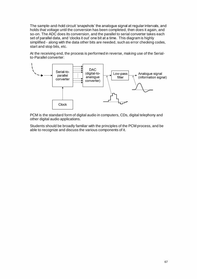
67
The sample-and-hold circuit ‘snapshots’ the analogue signal at regular intervals, and holds that voltage until the conversion has been completed, then does it again, and so-on. The ADC does its conversion, and the parallel to serial converter takes each set of parallel data, and ‘clocks it out’ one bit at a time. This diagram is highly simplified - along with the data other bits are needed, such as error checking codes, start and stop bits, etc.
At the receiving end, the process is performed in reverse, making use of the Serial-to-Parallel converter:
PCM is the standard form of digital audio in computers, CDs, digital telephony and other digital audio applications.
Students should be broadly familiar with the principles of the PCM process, and be able to recognize and discuss the various components of it.

68
Teacher Resource Bank
GCE Physics A
Equipment & materials resources:
Electronics by D.L. Faithfull.
The notes which follow are intended to be a guide to some of the materials and equipment resources which are either essential, or may be helpful for the delivery of the Electronics option. After some suggestions for general resources applicable to all topics, any resources specific to, or mainly for, a particular topic are given after each chapter heading.
General resources
1. Essential equipment includes:
i. Oscilloscope (ideal is a software-based device, such as the Pico range of instruments) a 10 MHz bandwidth is adequate, although a bandwidth of 20 MHz
is better and is likely to be a better all-round instrument.
ii. Multimeters – DC and AC voltage ranges, resistance and continuity.
iii. DC power supplies (up to 15 V at 1 A is adequate).
iv. Signal generator, covering the range 10 Hz–100 kHz, sine and square wave.
v. Soldering irons and associated tools.
vi. Prototyping boards.
There should ideally be enough of all of these for at least one between two students.
2. Equipment which could enhance the course but is not essential includes:
i. A signal generator with amplitude and frequency modulation capability (for demonstrating AM and FM).
ii. An inductance and a capacitance meter (though some multimeters have this capability).
iii. A logic analyser (these can be obtained as add-ons to a regular oscilloscope, and may be included in the software for PC-based oscilloscopes).
iv. An optical fibre demonstration kit.
3. Essential components and materials include the following:
i. A resistor kit - the E24 series.
ii. A capacitor kit; this should cover the range 1 nF–470 nF (ceramic) and μ – 1 μ (electrolytic – 25 V working minimum).
iii. A range of inductors: μH–100 mH.
iv. Diodes – the 1N4148 is the staple device for low current (signal) use, the 1N4001 for higher currents (up to 1 A).
v. Hook-up wire (wire links) for use on prototype boards.

69
Chapter 1 Discrete semiconductor devices (specification reference 3.13.1)
Components specifically needed or recommended for this chapter are listed. There should be enough of these for all students to investigate the topics in this chapter, working in pairs:
i. MOSFET. Suitable types are the BS170, ZVN2016A, ZVN3306 low power types, or IRF830, IRL3303 high power. All are cheap.
ii. Zener diodes. The BZX55 range (500 mW rating) is suitable. A selection, say
3.3 V, 4.7 V, 5.1 V, 5.6 V, 6.8 V and 10 V would be suitable.
iii. Photodiode. A visible range device, reasonably priced, is the BPX65.
iv. Hall effect device. The SS495A2 from RS, which gives an analogue output, is suitable. There are others with on-board amplification and circuitry to provide a digital output, such as the SS41 from Rapid if this is wanted: it makes demonstrating the use of the device as the sensor in a tachometer much easier.
v. A magnet, for use with the Hall effect device.
vi. A microphone. A high-output crystal microphone is cheap and gives the biggest signal – and poorest quality – but may not be easily available. A good alternative is a miniature electret PCB mounting microphone module; this has to be connected to a power supply.
vii. A comparison of the differences between LDR and photodiode can be set up with a few components.
1. Laser pointer.
2. LDR (NORP12 is a common type).
3. Photodiode (the BPX65 is a typical visible range device).
4. 7 MΩ and Ω resistors.
5. Oscilloscope.
6. A short length of optical fibre.
The arrangement for the photodiode is as shown below.
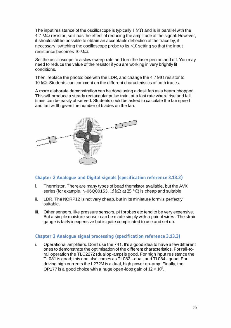
70
The input resistance of the oscilloscope is typically MΩ and is in parallel with the
7 MΩ resistor, so it has the effect of reducing the amplitude of the signal. However, it should still be possible to obtain an acceptable deflection of the trace by, if
necessary, switching the oscilloscope probe to its ×10 setting so that the input
resistance becomes MΩ.
Set the oscilloscope to a slow sweep rate and turn the laser pen on and off. You may need to reduce the value of the resistor if you are working in very brightly lit conditions.
Then, replace the photodiode with the LDR, and change the 7 MΩ resistor to
10 Ω. Students can comment on the different characteristics of both traces.
A more elaborate demonstration can be done using a desk fan as a beam ‘chopper’. This will produce a steady rectangular pulse train, at a fast rate where rise and fall times can be easily observed. Students could be asked to calculate the fan speed and fan width given the number of blades on the fan.
Chapter 2 Analogue and Digital signals (specification reference 3.13.2)
i. Thermistor. There are many types of bead thermistor available, but the AVX series (for example, N-06Q00153, Ω at 25 °C) is cheap and suitable.
ii. LDR. The NORP12 is not very cheap, but in its miniature form is perfectly suitable.
iii. Other sensors, like pressure sensors, pH probes etc tend to be very expensive. But a simple moisture sensor can be made simply with a pair of wires. The strain gauge is fairly inexpensive but is quite complicated to use and set up.
Chapter 3 Analogue signal processing (specification reference 3.13.3)
i. Operational amplifiers. Don’t use the 741. It’s a good idea to have a few different ones to demonstrate the optimisation of the different characteristics. For rail-to-rail operation the TLC2272 (dual op-amp) is good. For high input resistance the TL081 is good; this one also comes as TL082 –dual, and TL084 - quad. For driving high currents the L272M is a dual, high power op-amp. Finally, the
OP177 is a good choice with a huge open-loop gain of 12 × 106.

71
Chapter 4 Operational amplifier circuits (specification reference 3.13.4)
i. A variety of different signal sources is good for this section, especially to show the behaviour of the summing amplifier. For example, a signal generator, a CD player and a microphone.
ii. If you have the time to build it, a simple ECG amplifier, using just one op-amp, can be constructed, which demonstrates very effectively the noise-cancelling behaviour of the differential amplifier. A differential gain of about 1000 is needed for a good signal to display on the oscilloscope.
Chapter 5 Digital signal processing (specification reference 3.13.5)
i. A number of different logic families can be used for teaching. However, the CMOS 4000B series is ideal. It operates over a range of supply voltages from 3 V to about 15 V and has very low power consumption. The series is, however,
static sensitive, so modest handling precautions are advised (though, in practice,protective circuits within the chips tend to make it fairly robust). An inconvenience, as a result of the very high input resistance, is that any unused inputs on the chip have to be tied to + or – supply (as appropriate). ‘Floating’ inputs will produce erroneous behaviour.
ii. A minimum selection of the following CMOS chips is recommended:
4001 quad 2-input NOR gate
4011 quad 2-input NAND gate
4017 decade counter with 10 decoded outputs (5-stage Johnson counter)
4020 14-stage binary ripple counter
4024 7-stage binary ripple counter
4026 decade counter with decoded 7-segment display outputs and display enable
4029 pre-settable up/down counter, binary or BCD-decade
4040 12-stage binary ripple counter
4049 hex inverter
4060 14-stage binary ripple counter and oscillator
4070 quad 2-input XOR gate
4071 quad 2-input OR gate
4081 quad 2-input AND gate
4106 hex Schmitt trigger
4511 BCD to 7-segment latch/decoder/driver
4518 dual BCD up counter
4541 programmable timer

72
Chapter 6 Data communication systems (specification reference 3.13.6)
i. A length of fibre optic cable.
ii. An FM radio. This is good for illustrating how the broadcast radio band is divided up. Also, a simple single-transistor FM transmitter can be built (very low power, so not illegal – but check Ofcom regulations before doing this, to make sure) which can be used to demonstrate FM radio signals.
iii. A crystal radio set. Actually, although there are many kits out there, the bits can be bought quite cheaply, and it’s quite helpful in getting across the principles of radio signals to have students build their own. With a length of about 20 m of
wire hanging out of the window a range of AM transmissions can be received.
iv. A 433 MHz transmitter/receiver pair. These can be bought from Maplin for about
£4 for the transmitter, and £6 for the receiver. A great investment, the transmitter accepts a digital input, and the system can be used to very effectively
demonstrate telemetry and remote control. As it is 433 MHz it is licence exempt, so there’s no problem in using it to set up a data link across the school site.
An excellent theory and practical resource is the series of support booklets written for the AQA Electronics GCE by Ian Kemp. Although it covers topics in far greater detail, and includes many other topics besides, it is an ideal companion to this guide.
The suite of booklets can be downloaded at ikes.freeserve.co.uk/ .