tda2050 - 32w hi-fi audio power amplifier...
TRANSCRIPT
TDA2050
32W Hi-Fi AUDIO POWER AMPLIFIER
HIGH OUTPUT POWER(50W MUSIC POWER IEC 268.3 RULES)HIGH OPERATING SUPPLY VOLTAGE (50V)SINGLE OR SPLIT SUPPLY OPERATIONSVERY LOW DISTORTIONSHORT CIRCUIT PROTECTION (OUT TOGND)THERMAL SHUTDOWN
DESCRIPTIONThe TDA 2050 is a monolithic integrated circuit inPentawatt package, intended for use as an audioclass AB audio amplifier. Thanks to its high powercapability the TDA2050 is able to provide up to35W true rms power into 4 ohm load @ THD =10%, VS = ±18V, f = 1KHz and up to 32W into8ohm load @ THD = 10%, VS = ±22V, f = 1KHz.Moreover, the TDA 2050 delivers typically 50Wmusic power into 4 ohm load over 1 sec at VS=22.5V, f = 1KHz.
The high power and very low harmonic and cross-over distortion (THD = 0.05% typ, @ VS = ±22V,PO = 0.1 to 15W, RL=8ohm, f = 100Hz to 15KHz)make the device most suitable for both HiFi andhigh class TV sets.
This is advanced information on a new product now in development or undergoing evaluation. Details are subject to change without notice.
March 2002
®
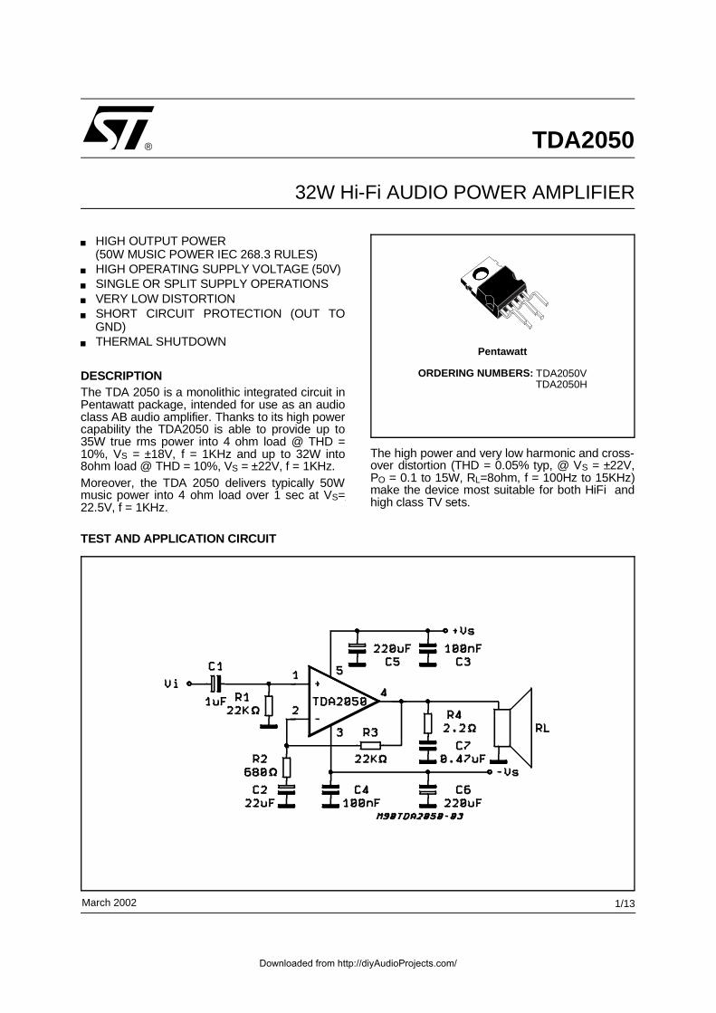
TEST AND APPLICATION CIRCUIT
Pentawatt
ORDERING NUMBERS: TDA2050V TDA2050H
1/13
Downloaded from http://diyAudioProjects.com/
SCHEMATIC DIAGRAM
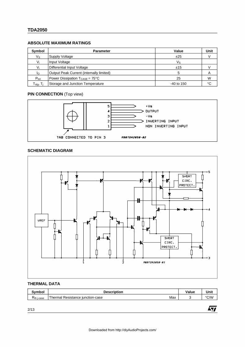
ABSOLUTE MAXIMUM RATINGS
Symbol Parameter Value Unit
VS Supply Voltage ±25 V
Vi Input Voltage VS
Vi Differential Input Voltage ±15 V
IO Output Peak Current (internally limited) 5 A
Ptot Power Dissipation TCASE = 75°C 25 W
Tstg, Tj Storage and Junction Temperature -40 to 150 °C
THERMAL DATA
Symbol Description Value Unit
Rth j-case Thermal Resistance junction-case Max 3 °C/W
PIN CONNECTION (Top view)
TDA2050
2/13
Downloaded from http://diyAudioProjects.com/

ELECTRICAL CHARACTERISTICS (Refer to the Test Circuit, VS = ±18V, Tamb = 25°C, f = 1 kHz; un-less otherwise specified)
Symbol Parameter Test Condition Min. Typ. Max. Unit
VS Supply Voltage Range ±4.5 ±25 V
Id Quiescent Drain Current VS = ±4.5VVS = ±25V
3055
5090
mAmA
Ib Input Bias Current VS = ±22V 0.1 0.5 µA
VOS Input Offset Voltage VS = ±22V ±15 mV
IOS Input Offset Current VS = ±22V ±200 nA
PO RMS Output Power d = 0.5%RL = 4ΩRL = 8ΩVS = ±22V RL = 8Ω
24
22
281825
WWW
d = 10%RL = 4ΩRL = 8ΩVS = ±22V RL = 8Ω
352232
WWW
Music PowerIEC268.3 RULES
d = 10%; T = 1sVS = ±22.5V; RL = 4Ω 50 W
d Total Harmonic Distortion RL = 4Ωf = 1kHz, PO = 0.1 to 24Wf = 100Hz to 10kHz, PO = 0.1 to 18W
0.03 0.50.5
%%
VS = ±22V RL = 8Ωf = 1kHz, PO = 0.1 to 20Wf = 100Hz to 10kHz, PO = 0.1 to 15W
0.020.5
%%
SR Slew Rate 5 8 V/µs
GV Open Loop Voltage Gain 80 dB
GV Closed Loop Voltage Gain 30 30.5 31 dB
BW Power Bandwidth (-3dB) RL = 4Ω Vi = 200mV 20 to 80,000 Hz
eN Total Input Noise curve AB = 22Hz to 22kHz
45 10
µVµV
Ri Input Resistance (pin 1) 500 kΩSVR Supply Voltage Rejection Rs = 22kΩ; f = 100Hz;
Vripple = 0.5Vrms 45 dB
η Efficiency PO = 28W; RL = 4Ω 65 %
PO = 25W; RL = 8Ω;VS = ±22V 67 %
Tsd-j Thermal Shut-downJunction Temperature
150 °C
TDA2050
3/13
Downloaded from http://diyAudioProjects.com/
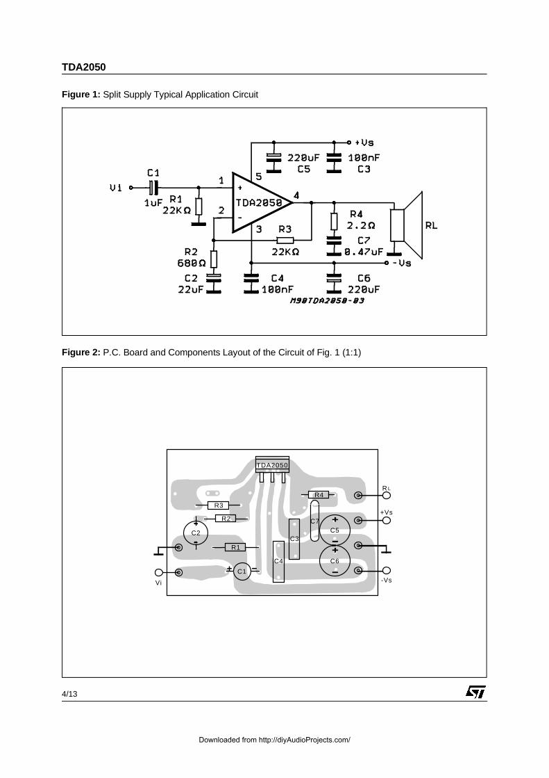
Figure 1: Split Supply Typical Application Circuit
R3
R2
R1
C2
C4
C3
R4
C5
C6
C1
C7+Vs
R L
-Vs
TDA2050
Vi
Figure 2: P.C. Board and Components Layout of the Circuit of Fig. 1 (1:1)
TDA2050
4/13
Downloaded from http://diyAudioProjects.com/

SPLIT SUPPLY APPLICATION SUGGESTIONSThe recommended values of the external compo-nents are those shown on the application circuit
of fig. 2. Different values can be used. The follow-ing table can help the designer.
Component RecommendedValue Purpose Larger than
Recommended ValueSmaller than
Recommended Value
R1 22kΩ Input Impedance Increase of InputImpedance
Decrease of InputImpedance
R2 680Ω Feedback Resistor Decrease of Gain (*) Increase of Gain
R3 22kΩ Increase of Gain Decrease of Gain (*)
R4 2.2Ω Frequency Stability Danger of Oscillations
C1 1µF Input Decoupling DC Higher Low-frequencycut-off
C2 22µF Inverting InputDC Decoupling
Increase of SwitchON/OFF Noise
Higher Low-frequencycut-off
C3C4
100nF Supply Voltage Bypass Danger of Oscillations
C5C6
220µF Supply Voltage Bypass Danger of Oscillations
C7 0.47µF Frequency Stability Danger of Oscillations
(*) The gain must be higher than 24dB
PRINTED CIRCUIT BOARDThe layout shown in fig. 2 should be adopted bythe designers. If different layouts are used, the
ground points of input 1 and input 2 must be welldecoupled from the ground return of the output inwhich a high current flows.
TDA2050
5/13
Downloaded from http://diyAudioProjects.com/
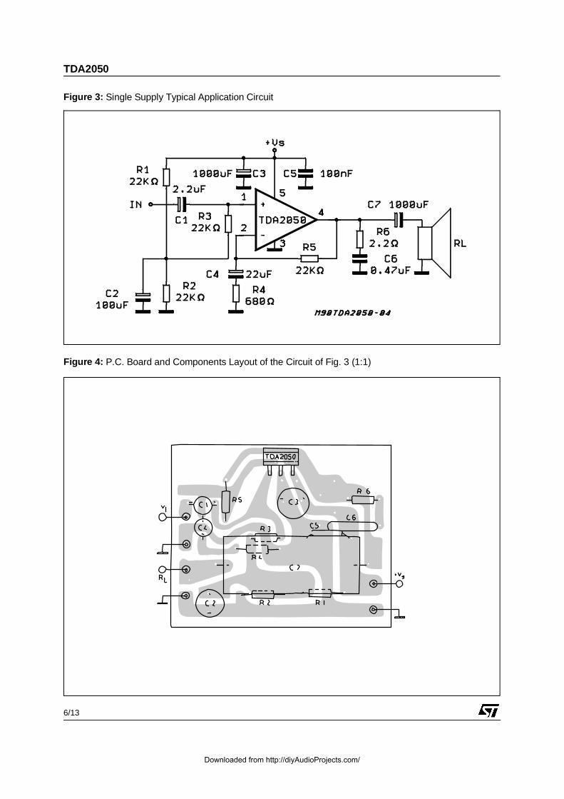
Figure 3: Single Supply Typical Application Circuit
Figure 4: P.C. Board and Components Layout of the Circuit of Fig. 3 (1:1)
TDA2050
6/13
Downloaded from http://diyAudioProjects.com/

SINGLE SUPPLY APPLICATION SUGGESTIONSThe recommended values of the external compo-nents are those shown on the application circuit
of fig. 3. Different values can be used. The follow-ing table can help the designer.
Component RecommendedValue Purpose Larger than
Recommended ValueSmaller than
Recommended Value
R1, R2, R3 22kΩ Biasing Resistor
R4 680ΩFeedback Resistors
Increase of Gain Decrease of Gain (*)
R5 22kΩ Decrease of Gain (*) Increase of Gain
R6 2.2Ω Frequency Stability Danger of Oscillations
C1 2.2µF Input Decoupling DC Higher Low-frequencycut-off
C2 100µF Supply Voltage Rejection Worse Turn-off TransientWorse Turn-on Delay
C3 1000µF Supply Voltage Bypass Danger of OscillationsWorse of Turn-offTransient
C4 22µF Inverting Input DCDecoupling
Increase of SwitchingON/OFF
Higher Low-frequencycut-off
C5 100nF Supply Voltage Bypass Danger of Oscillations
C6 0.47µF Frequency Stability Danger of Oscillations
C7 1000µF Output DC Decoupling Higher Low-frequencycut-off
(*) The gain must be higher than 24dB
TYPICAL CHARACTERISTICS (Split Supply Test Circuit unless otherwise specified)
NOTEIf the supply voltage is lower than 40V and theload is 8ohm (or more) a lower value of C2 can
be used (i.e. 22µF).C7 can be larger than 1000uF only if the supplyvoltage does not exceed 40V.
Figure 5: Output Power vs. Supply VoltageFigure 6: Distortion vs. Output Power
TDA2050
7/13
Downloaded from http://diyAudioProjects.com/
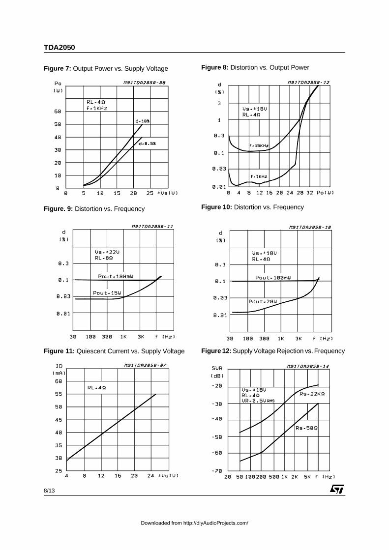
Figure 10: Distortion vs. FrequencyFigure. 9: Distortion vs. Frequency
Figure 8: Distortion vs. Output Power
Figure 12: Supply Voltage Rejection vs. FrequencyFigure 11: Quiescent Current vs. Supply Voltage
Figure 7: Output Power vs. Supply Voltage
TDA2050
8/13
Downloaded from http://diyAudioProjects.com/
SHORT CIRCUIT PROTECTIONThe TDA 2050 has an original circuit which limitsthe current of the output transistors. The maxi-mum output current is a function of the collectoremitter voltage; hence the output transistors workwithin their safe operating area. This function cantherefore be considered as being peak power lim-iting rather than simple current limiting.It reduces the possibility that the device getsdamaged during an accidental short circuit fromAC output to ground.
THERMAL SHUTDOWNThe presence of a thermal limiting circuit offersthe following advantages:
1)An overload on the output (even if it is perma-nent), or an above limit ambient temperaturecan be easily tolerated since the Tj cannot behigher than 150°C.
2)The heatsink can have a smaller factor ofsafety compared with that of a conventionalcircuit. There is no possibility of device dam-age due to high junction temperature. If forany reason, the junction temperature in-creases up to 150°C, the thermal shutdownsimply reduces the power dissipation and thecurrent consumption.
The maximum allowable power dissipation de-pends upon the thermal resistance junction-ambi-
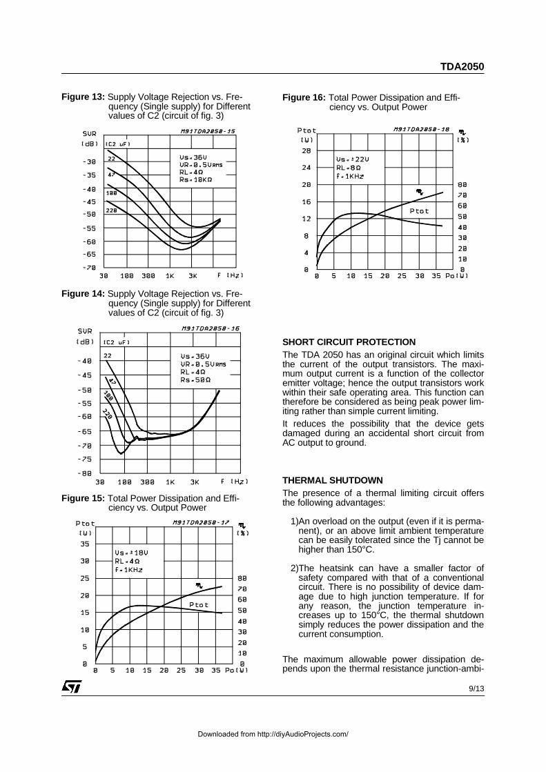
Figure 13: Supply Voltage Rejection vs. Fre-quency (Single supply) for Differentvalues of C2 (circuit of fig. 3)
Figure 14: Supply Voltage Rejection vs. Fre-quency (Single supply) for Differentvalues of C2 (circuit of fig. 3)
Figure 15: Total Power Dissipation and Effi-ciency vs. Output Power
Figure 16: Total Power Dissipation and Effi-ciency vs. Output Power
TDA2050
9/13
Downloaded from http://diyAudioProjects.com/
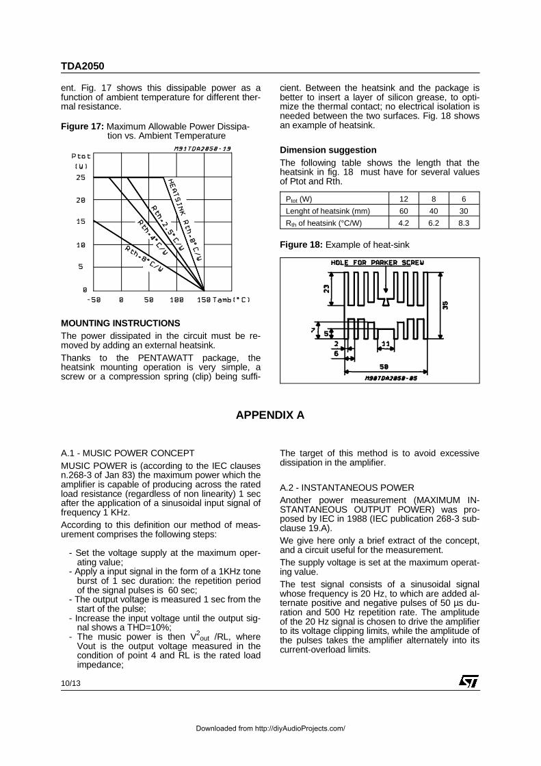
ent. Fig. 17 shows this dissipable power as afunction of ambient temperature for different ther-mal resistance.
MOUNTING INSTRUCTIONSThe power dissipated in the circuit must be re-moved by adding an external heatsink.Thanks to the PENTAWATT package, theheatsink mounting operation is very simple, ascrew or a compression spring (clip) being suffi-
cient. Between the heatsink and the package isbetter to insert a layer of silicon grease, to opti-mize the thermal contact; no electrical isolation isneeded between the two surfaces. Fig. 18 showsan example of heatsink.
Dimension suggestionThe following table shows the length that theheatsink in fig. 18 must have for several valuesof Ptot and Rth.
Ptot (W) 12 8 6
Lenght of heatsink (mm) 60 40 30
Rth of heatsink (°C/W) 4.2 6.2 8.3
Figure 18: Example of heat-sink
Figure 17: Maximum Allowable Power Dissipa-tion vs. Ambient Temperature
A.1 - MUSIC POWER CONCEPTMUSIC POWER is (according to the IEC clausesn.268-3 of Jan 83) the maximum power which theamplifier is capable of producing across the ratedload resistance (regardless of non linearity) 1 secafter the application of a sinusoidal input signal offrequency 1 KHz.According to this definition our method of meas-urement comprises the following steps:
- Set the voltage supply at the maximum oper-ating value;
- Apply a input signal in the form of a 1KHz toneburst of 1 sec duration: the repetition periodof the signal pulses is 60 sec;
- The output voltage is measured 1 sec from thestart of the pulse;
- Increase the input voltage until the output sig-nal shows a THD=10%;
- The music power is then V2out /RL, where
Vout is the output voltage measured in thecondition of point 4 and RL is the rated loadimpedance;
The target of this method is to avoid excessivedissipation in the amplifier.
A.2 - INSTANTANEOUS POWERAnother power measurement (MAXIMUM IN-STANTANEOUS OUTPUT POWER) was pro-posed by IEC in 1988 (IEC publication 268-3 sub-clause 19.A).We give here only a brief extract of the concept,and a circuit useful for the measurement.The supply voltage is set at the maximum operat-ing value.The test signal consists of a sinusoidal signalwhose frequency is 20 Hz, to which are added al-ternate positive and negative pulses of 50 µs du-ration and 500 Hz repetition rate. The amplitudeof the 20 Hz signal is chosen to drive the amplifierto its voltage clipping limits, while the amplitude ofthe pulses takes the amplifier alternately into itscurrent-overload limits.
APPENDIX A
TDA2050
10/13
Downloaded from http://diyAudioProjects.com/
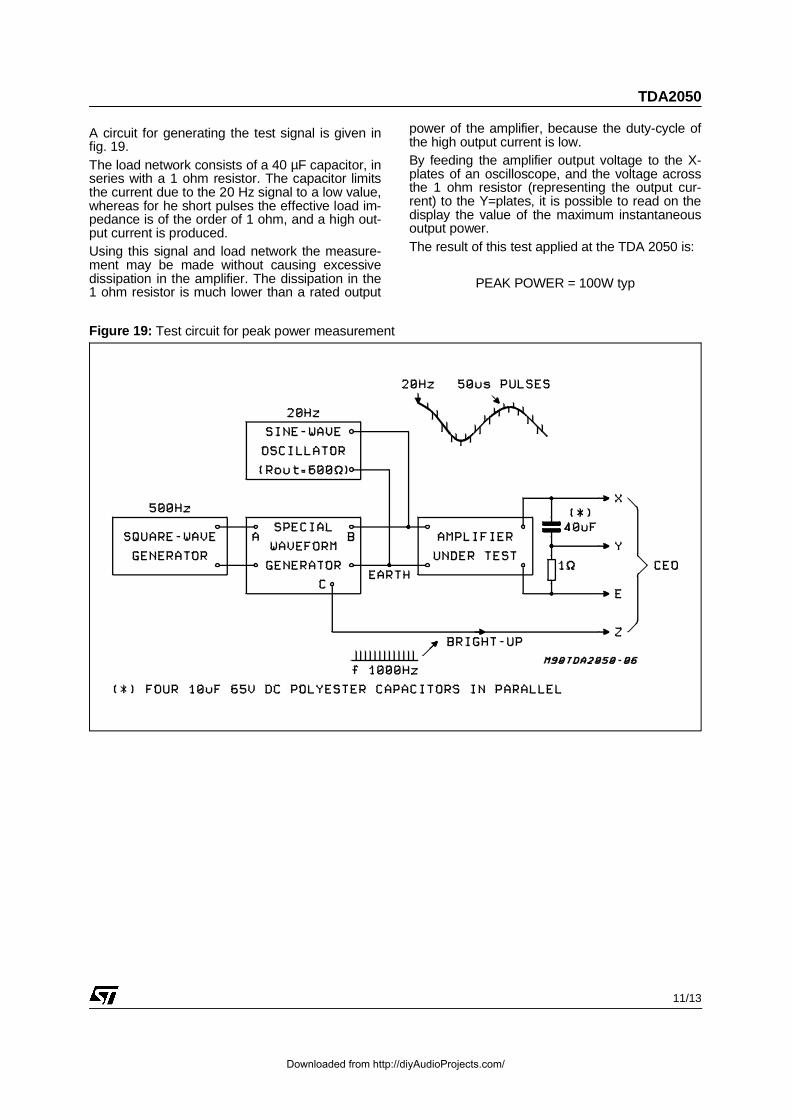
A circuit for generating the test signal is given infig. 19.The load network consists of a 40 µF capacitor, inseries with a 1 ohm resistor. The capacitor limitsthe current due to the 20 Hz signal to a low value,whereas for he short pulses the effective load im-pedance is of the order of 1 ohm, and a high out-put current is produced.Using this signal and load network the measure-ment may be made without causing excessivedissipation in the amplifier. The dissipation in the1 ohm resistor is much lower than a rated output
power of the amplifier, because the duty-cycle ofthe high output current is low.By feeding the amplifier output voltage to the X-plates of an oscilloscope, and the voltage acrossthe 1 ohm resistor (representing the output cur-rent) to the Y=plates, it is possible to read on thedisplay the value of the maximum instantaneousoutput power.The result of this test applied at the TDA 2050 is:
PEAK POWER = 100W typ
Figure 19: Test circuit for peak power measurement
TDA2050
11/13
Downloaded from http://diyAudioProjects.com/
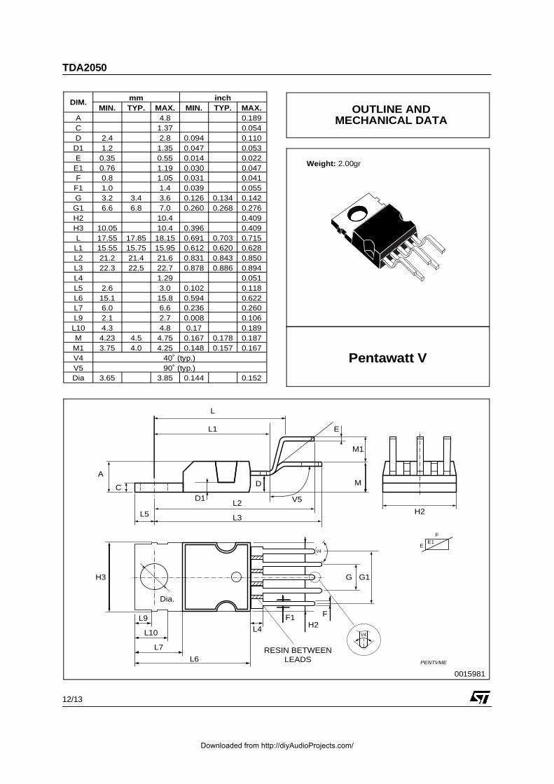
Weight: 2.00gr
Pentawatt V
DIM. mm inchMIN. TYP. MAX. MIN. TYP. MAX.
A 4.8 0.189C 1.37 0.054D 2.4 2.8 0.094 0.110
D1 1.2 1.35 0.047 0.053E 0.35 0.55 0.014 0.022
E1 0.76 1.19 0.030 0.047F 0.8 1.05 0.031 0.041
F1 1.0 1.4 0.039 0.055G 3.2 3.4 3.6 0.126 0.134 0.142
G1 6.6 6.8 7.0 0.260 0.268 0.276H2 10.4 0.409H3 10.05 10.4 0.396 0.409L 17.55 17.85 18.15 0.691 0.703 0.715
L1 15.55 15.75 15.95 0.612 0.620 0.628L2 21.2 21.4 21.6 0.831 0.843 0.850L3 22.3 22.5 22.7 0.878 0.886 0.894L4 1.29 0.051L5 2.6 3.0 0.102 0.118L6 15.1 15.8 0.594 0.622L7 6.0 6.6 0.236 0.260L9 2.1 2.7 0.008 0.106
L10 4.3 4.8 0.17 0.189M 4.23 4.5 4.75 0.167 0.178 0.187
M1 3.75 4.0 4.25 0.148 0.157 0.167V4 40˚ (typ.)V5 90˚ (typ.)Dia 3.65 3.85 0.144 0.152
L
L1
A
C
L5
D1L2
L3
E
M1
MD
H3
Dia.
L7
L9
L10
L6
F1H2
F
G G1
E1F
E
V4
RESIN BETWEENLEADS
H2
V5
V4
PENTVME
L4
0015981
OUTLINE ANDMECHANICAL DATA
TDA2050
12/13
Downloaded from http://diyAudioProjects.com/
Information furnished is believed to be accurate and reliable. However, STMicroelectronics assumes no responsibility for the consequencesof use of such information nor for any infringement of patents or other rights of third parties which may result from its use. No license isgranted by implication or otherwise under any patent or patent rights of STMicroelectronics. Specification mentioned in this publication aresubject to change without notice. This publication supersedes and replaces all information previously supplied. STMicroelectronics productsare not authorized for use as critical components in life support devices or systems without express written approval of STMicroelectronics.
The ST logo is a registered trademark of STMicroelectronics© 2002 STMicroelectronics – Printed in Italy – All Rights Reserved
PENTAWATT® is a Registered Trademark of SGS-THOMSON MicroelectronicsSTMicroelectronics GROUP OF COMPANIES
Australia - Brazil - Canada - China - Finland - France - Germany - Hong Kong - India - Israel - Italy - Japan - Malaysia - Malta - Morocco -Singapore - Spain - Sweden - Switzerland - United Kingdom - United States.
http://www.st.com
TDA2050
13/13
Downloaded from http://diyAudioProjects.com/