tda18211hd dvb-t silicon tuner ic - digi-key sheets/nxp pdfs/tda18211hd.pdf · dvb-t silicon tuner...
TRANSCRIPT

1. General description
The TDA18211HD is a Silicon Tuner IC designed for digital terrestrial (DVB-T) TVreception. The TDA18211HD integrates the overall tuning function, including selectivity,and provides a low-IF output signal.
The TDA18211HD uses integrated IF filters to support 6/7/8 MHz channel bandwidths.The TDA18211HD requires only one single 16 MHz crystal for clock generation. A clocksignal is available on crystal oscillator output pins (XTOUTP/XTOUTN) to synchronize thechannel decoder and slave front end in case of DVR configuration.
This specification is based on software version 3.4
2. Features
n Fully integrated RF tracking filters for unwanted signal suppression
n Fully integrated IF selectivity (no need for external SAW filters)
n Fully integrated oscillators with no external components
n Integrated wideband gain control
n Alignment free
n RF loop-through for easy implementation in the STB
n Input power level indicator
n Integrated die thermal sensor
n Single 3.3 V power supply
n Low power consumption (780 mW)
n Crystal oscillator output buffer (16 MHz) to allow single crystal applications
n I2C-bus interface compatible with 3.3 V and 5 V microcontrollers
n Three Standby modes
n RoHS packaging
3. Applications
3.1 Target applicationsn DVB-T Set-Top-Box (STB) and TV receiver
n Application optimization is described in the application notes
TDA18211HDDVB-T Silicon Tuner ICRev. 05 — 2 June 2009 Product data sheet

NXP Semiconductors TDA18211HDDVB-T Silicon Tuner IC
3.2 Key benefitsn The TDA18211HD is a low cost Silicon Tuner targeting digital terrestrial applications.
The TDA18211HD matches the performance of the conventional can tuners whilereducing the size of the tuner function drastically. Additionally, the following benefitscan be stated:
u Allows easy on-board integration
u Allows easy dual-tuner configuration
u Drastically reducing the size of the tuner function and power consumption
4. Quick reference data
[1] Measured with TDA10048HN channel decoder.
5. Ordering information
Table 1. Quick reference dataTamb = 25 °C; VCC = 3.3 V; IF output level option = 2 V (p-p); IF output load = 1 kΩ on each terminal.
Symbol Parameter Conditions Min Typ Max Unit
fRF RF frequency center of channel 174 - 864 MHz
NFtun tuner noise figure maximum gain - 5.5 6 dB
ϕn phase noise - −89 - dBc/Hz
P power dissipation - 780 - mW
Vi(max) maximum inputvoltage
1 dB gain compression, oneanalog TV signal at RF input(−5 dBm)
- 103 - dBµV
αimage image rejection 53 65 - dB
Sdig digital sensitivity DVB-T (64 QAM 2⁄3);BER = 2.10−4
[1] - −82 - dBm
Table 2. Ordering information
Type number Package
Name Description Version
TDA18211HD/C2 HLQFN64R plastic thermal enhanced low profile quad flatpackage; no leads; 64 terminals; resin based;body 9 × 9 × 1.6 mm
SOT903-1
TDA18211HD_5 © NXP B.V. 2009. All rights reserved.
Product data sheet Rev. 05 — 2 June 2009 2 of 66

NXP Semiconductors TDA18211HDDVB-T Silicon Tuner IC
6. Block diagram
Fig 1. Block diagram
001aag932
AGC CONTROL
ATTENUATORS
TDA18211HDTEST SIGNALGENERATOR
CALIBRATIONSYNTHESIZER
MAINSYNTHESIZER
DUAL TUNERPROTOCOL
DIVIDERcrystal
oscillator
DC-to-DCCONVERTER
DIGITALCIRCUITRY
LCtrackingfilters
RFpolyphase
filter
IFpolyphase
filter
IFlow-pass
filter
VT_CAL CP_CAL
XTALP
CP_LO
XTALN VT_FINE
VT_COARSE
RFAGC
IFAGC
IFOUTNIFOUTP
V_IFAGC
45
FREEZE28
MASTERSYNC19
4647AGC
VCO
LNA
AGC1 AGC2
RF_IN 10
13
15
CONTROLINTERFACE
SCLAS SDA
3832 39 35 34 26 2227 24 21
LT
STO
mixer
TDA18211HD_5 © NXP B.V. 2009. All rights reserved.
Product data sheet Rev. 05 — 2 June 2009 3 of 66

NXP Semiconductors TDA18211HDDVB-T Silicon Tuner IC
7. Pinning information
7.1 Pinning
7.2 Pin description
Fig 2. Pin configuration
TDA18211HD
48
47
46
45
44
43
42
41
40
39
38
37
36
35
34
33
GND
V_IFAGC
IFOUTP
IFOUTN
VCC
GND
CAPREG28
GND
CAPREG18
SDA
SCL
GND
GND
VT_CAL
CP_CAL
VCC
GND
GND
GND
GND
GND
GND
GND
n.c.
VCC
RF_IN
GND
CAPRFAGC
LT
GND
STO
VCC
CA
PR
EG
VC
O
VC
C
MA
ST
ER
SY
NC
CA
PF
ILT
VC
O
VT
_CO
AR
SE
VT
_FIN
E
GN
D
CP
_LO
GN
D
XT
ALP
XT
ALN
FR
EE
ZE
XT
OU
T_M
S
XT
OU
TP
XT
OU
TN
AS
GN
D
GN
D
GN
D
GN
D
GN
D
GN
D
GN
D
GN
D
GN
D
GN
D
GN
D
GN
D
CA
PR
EG
FIL
TR
F
VS
YN
C
GN
D
GN
D
1
2
3
4
5
6
7
8
9
10
11
12
13
14
15
16
64 63 62 61 60 59 58 57 56 55 54 53 52 51 50 49
17 18 19 20 21 22 23 24 25 26 27 28 29 30 31 32
Transparent top view
terminal 1index area
001aaf832
Table 3. Pin description
Symbol Pin Description
GND 1 to 7 ground
n.c. 8 not connected
VCC 9 3.3 V supply voltage
RF_IN 10 unbalanced RF (TV) input
GND 11 ground
CAPRFAGC 12 RF AGC filtering
LT 13 loop-through output
TDA18211HD_5 © NXP B.V. 2009. All rights reserved.
Product data sheet Rev. 05 — 2 June 2009 4 of 66

NXP Semiconductors TDA18211HDDVB-T Silicon Tuner IC
GND 14 ground
STO 15 slave tuner output
VCC 16 3.3 V supply voltage
CAPREGVCO 17 VCO supply decoupling
VCC 18 3.3 V supply voltage
MASTERSYNC 19 synchronization signal for dual-tuner applications; leave open forsingle-tuner applications
CAPFILTVCO 20 VCO reference decoupling
VT_COARSE 21 LO oscillator tuning voltage input
VT_FINE 22 LO oscillator tuning voltage input
GND 23 ground
CP_LO 24 charge pump of the local synthesizer
GND 25 ground
XTALP 26 crystal oscillator input
XTALN 27 crystal oscillator input
FREEZE 28 synchronization signal for multi-tuner applications; leave open forsingle-tuner applications
XTOUT_MS 29 XTOUT mode and master/slave selection input
XTOUTP 30 crystal oscillator output buffer
XTOUTN 31 crystal oscillator output buffer
AS 32 I2C-bus address selection input
VCC 33 3.3 V supply voltage
CP_CAL 34 charge pump of the calibration synthesizer
VT_CAL 35 tuning voltage of the calibration synthesizer
GND 36, 37 ground
SCL 38 I2C-bus clock input
SDA 39 I2C-bus data input/output
CAPREG18 40 internal regulator decoupling
GND 41 ground
CAPREG28 42 internal regulator decoupling
GND 43 ground
VCC 44 3.3 V supply voltage
IFOUTN 45 IF output
IFOUTP 46 IF output
V_IFAGC 47 IF gain control input
GND 48 to 50 ground
VSYNC 51 vertical synchronization input for analog applications; connect toground for digital applications
CAPREGFILTRF 52 internal regulator decoupling
GND 53 to 64 ground
- exposeddie
ground
Table 3. Pin description …continued
Symbol Pin Description
TDA18211HD_5 © NXP B.V. 2009. All rights reserved.
Product data sheet Rev. 05 — 2 June 2009 5 of 66

NXP Semiconductors TDA18211HDDVB-T Silicon Tuner IC
8. Functional description
The RF input signal is driven to a low-noise amplifier. It is then band-pass filtered,amplified and fed to the image rejection mixer. The mixer downconverts the RF signal to alow IF, which depends on channel bandwidth (standard IF filters are implemented for6/7/8 MHz channel bandwidths; see Table 41).
The gain between the antenna pin (pin RF_IN) and the loop-through pin (pin LT) is 0 dB.
The TDA18211HD requires a single 16 MHz crystal for clock generation.
When bit XTOUT_ON = 1, a differential sine wave clock reference is available on pinsXTOUTP and XTOUTN to drive a channel decoder.
8.1 Master and slave operationThe TDA18211HD allows easy dual-tuner configuration.
Each individual tuner has to be set either in Master mode or Slave mode by applying a DCvoltage on the XTOUT_MS pin; see Table 4. This will decide whether the crystal oscillatorpart is used as negative impedance connected to the crystal part or as a current buffer.
In dual-tuner application:
• The first tuner is set in Master mode
• The second tuner has to be set in Slave mode
In single-tuner application:
• The tuner must be set in Master mode.
8.2 Tuner outputsThe tuner provides a slave tuner output (pin STO) and a loop-through output (pin LT).Those outputs are used to transmit the antenna signal to other tuners. Each output has itsown characteristics (see Table 56 and Table 57)
8.2.1 Loop-through output
The gain between the antenna connector and the loop-through pin (pin LT) equals 0 dB.This pin can be connected to any consumer electronic equipment.
8.2.2 Slave tuner output
The slave tuner output (pin STO) must be connected to the RF input of the slave tunerTDA18211HD in case of dual-tuner applications.
The gain between the antenna connector and the slave tuner output can changeaccording to the input level. The slave tuner will automatically compensate the gainchange, using the MASTERSYNC and FREEZE signals.
Table 4. Master and slave selection
Voltage on pin XTOUT_MS Tuner type Crystal oscillator
0 V to 0.1VCC master negative impedance presented to the crystal
0.4VCC to 0.6VCC slave current input buffer
TDA18211HD_5 © NXP B.V. 2009. All rights reserved.
Product data sheet Rev. 05 — 2 June 2009 6 of 66

NXP Semiconductors TDA18211HDDVB-T Silicon Tuner IC
8.3 Crystal input modeThe TDA18211HD requires a 16 MHz crystal reference. The chosen crystal mustwithstand at least 100 µW drive level. An additional shunt capacitor as shown in Figure 1is also needed. Its typical value is 5.6 pF. The quartz references for which performance isguaranteed are:
• NDK NX5032
• Siward SX-5032
• TXC 9C series
• Chungho Elcom HC49/S profile
Clock reference:
• In Master mode, the clock reference must be provided by a 16 MHz crystal connectedbetween pins XTALP and XTALN of the master tuner
• In Slave mode, the clock reference must be provided by pins XTOUTP and XTOUTNof the tuner in Master mode to pins XTALP and XTALN of the tuner in Slave mode
8.4 Crystal output modePins XTOUTP and XTOUTN deliver a symmetrical sine waveform to drive the channeldecoder and/or IF demodulator. The load on both outputs should be made similar toensure optimum performances. Hence, if only one crystal output is used, the unusedoutput should be loaded by an equivalent capacitance.
9. Control interface
9.1 I2C-bus format, write/read modeRemark: In I2C-bus read mode, the TDA18211HD must read the entire I2C map with therequired subaddress 00h. The number of bytes to be read is 16, or 39 in extended registermode; see Table 7. Reading write-only bits can return values that are different from theprogrammed values.
TDA18211HD_5 © NXP B.V. 2009. All rights reserved.
Product data sheet Rev. 05 — 2 June 2009 7 of 66

xxxxxxxxxxxxxxxxxxxxx xxxxxxxxxxxxxxxxxxxxxxxxxx xxxxxxx x x x xxxxxxxxxxxxxxxxxxxxxxxxxxxxxx xxxxxxxxxxxxxxxxxxx xx xxxxxxx xxxxxxxxxxxxxxxxxxxxxxxxxxx xxxxxxxxxxxxxxxxxxx xxxxxx xxxxxxxxxxxxxxxxxxxxxxxxxxxxxxxxxxx xxxxxxxxxxxx x xxxxxxxxxxxxxxxxxxxxxx xxxxxxxxxxxxxxxxxxxxxxxxxxxxxx xxxxx xxxxxxxxxxxxxxxxxxxxxxxxxxxxxxxxxxxxxxxxxxxxxxxxxx xxxxxxxxxxxxxxxxxxxxxxxxxxxxxxxxx xxxxxxxxxxxxxxxxxxxx xxx
TD
A18211H
D_5
Product data shee
NX
P S
emiconductors
TD
A18211H
DD
VB
-T S
ilicon Tuner IC
Table 5. I2C-bus format
Name Bytename
Subaddress
Bit
7 6 5 4 3 2 1 0
Address byte 1 - - 1 1 0 0 0 MA[1] MA[0] R/W
]
TM_D[3:0]
BP_FILTER[2:0]
_TAPER[4:0]
STD[4:0]
CAL_MODE[1:0]
IR_MEAS[2:0]
]
ALVCO_FORLON
AGC1_ALWAYS_MASTERN
AGC1_FIRSTN
EB4[4:0]
© N
XP
B.V. 2009. A
ll rights reserved.
tR
ev. 05 — 2 June 2009
8 of 66
Address byte 2 - - 0 0 AD[5:0
ID byte ID 00h 1 ID[6:0]
Thermo byte TM 01h POR LOCK TM_RANGE TM_ON
Power level byte PL 02h POWER_LEVEL[7:0]
Easy Prog byte 1 EP1 03h POWER_LEVEL[8]
DIS_POWER_
LEVEL
0 RF_CAL_OK IR_CAL_OK
Easy Prog byte 2 EP2 04h RF_BAND[2:0] GAIN
Easy Prog byte 3 EP3 05h SM SM_LT SM_XT
Easy Prog byte 4 EP4 06h FM_RFN XTOUT_ON 1 IF_LEVEL[2:0]
Easy Prog byte 5 EP5 07h EXTENDED_REG
IR_GSTEP[2:0] 0
Cal Post-Divider byte CPD 08h CAL_POST_DIV[7:0]
Cal Divider byte 1 CD1 09h 0 CAL_DIV[22:16]
Cal Divider byte 2 CD2 0Ah CAL_DIV[15:8]
Cal Divider byte 3 CD3 0Bh CAL_DIV[7:0]
Main Post-Dividerbyte
MPD 0Ch IF_NOTCH MAIN_POST_DIV[6:0
Main Divider byte 1 MD1 0Dh 0 MAIN_DIV[22:16]
Main Divider byte 2 MD2 0Eh MAIN_DIV[15:8]
Main Divider byte 3 MD3 0Fh MAIN_DIV[7:0]
Extended byte 1 EB1 10h EB1[7:3] C
Extended byte 2 EB2 11h EB2[7:0]
Extended byte 3 EB3 12h EB3[7:0]
Extended byte 4 EB4 13h EB4[7:6] LO_FORCESRCE
Extended byte 5 EB5 14h EB5[7:0]
Extended byte 6 EB6 15h EB6[7:0]

xxxxxxxxxxxxxxxxxxxxx xxxxxxxxxxxxxxxxxxxxxxxxxx xxxxxxx x x x xxxxxxxxxxxxxxxxxxxxxxxxxxxxxx xxxxxxxxxxxxxxxxxxx xx xxxxxxx xxxxxxxxxxxxxxxxxxxxxxxxxxx xxxxxxxxxxxxxxxxxxx xxxxxx xxxxxxxxxxxxxxxxxxxxxxxxxxxxxxxxxxx xxxxxxxxxxxx x xxxxxxxxxxxxxxxxxxxxxx xxxxxxxxxxxxxxxxxxxxxxxxxxxxxx xxxxx xxxxxxxxxxxxxxxxxxxxxxxxxxxxxxxxxxxxxxxxxxxxxxxxxx xxxxxxxxxxxxxxxxxxxxxxxxxxxxxxxxx xxxxxxxxxxxxxxxxxxxx xxx
TD
A18211H
D_5
Product data shee
NX
P S
emiconductors
TD
A18211H
DD
VB
-T S
ilicon Tuner ICExtended byte 7 EB7 16h EB7[7:6] CAL_ EB7[4:0]
EB8[2:0]
[5:0]
EB12[3:0]
:0] EB13[1:0]
EB15[3:0]
AGC1_GAIN[1:0]
B20[4:0]
AGC2_GAIN[1:0]
IF_TOP[3:0]
ORCELP_FC2_EN
LP_FC[2] EB23[0]
Table 5. I2C-bus format …continued
Name Bytename
Subaddress
Bit
7 6 5 4 3 2 1 0
© N
XP
B.V. 2009. A
ll rights reserved.
tR
ev. 05 — 2 June 2009
9 of 66
FORCE_SRCE
Extended byte 8 EB8 17h CID_ALARM EB8[6:4] EB8[3]
Extended byte 9 EB9 18h EB9[7:0]
Extended byte 10 EB10 19h EB10[7:6] CID_GAIN
Extended byte 11 EB11 1Ah EB11[7:0]
Extended byte 12 EB12 1Bh EB12[7:6] PD_AGC1_DET
PD_AGC2_DET
Extended byte 13 EB13 1Ch EB13[7] RFC_K[2:0] RFC_M[1
Extended byte 14 EB14 1Dh RFC_CPROG[7:0]
Extended byte 15 EB15 1Eh EB15[7:4]
Extended byte 16 EB16 1Fh EB16[7:0]
Extended byte 17 EB17 20h EB17[7:0]
Extended byte 18 EB18 21h AGC1_LOOP_OFF
EB18[6:2]
Extended byte 19 EB19 22h EB19[7:0]
Extended byte 20 EB20 23h EB20[7:6] FORCE_LOCK
E
Extended byte 21 EB21 24h AGC2_LOOP_OFF
EB21[6:2]
Extended byte 22 EB22 25h EB22[7] RF_TOP[2:0]
Extended byte 23 EB23 26h EB23[7:3] F

NXP Semiconductors TDA18211HDDVB-T Silicon Tuner IC
9.2 I2C-bus at power-on reset
Table 6. I2C-bus at power-on reset [1]
Name Byte Subaddress Bit
7 6 5 4 3 2 1 0
Address byte 1 - - 1 1 0 0 0 MA[1] MA[0] X
Address byte 2 - - X X AD[5] AD[4] AD[3] AD[2] AD[1] AD[0]
ID byte ID 00h 1 0 0 0 0 1 0 0
Thermo byte TM 01h 1 0 0 0 X X X X
Power Level byte PL 02h X X X X X X X X
Easy Prog byte 1 EP1 03h X 1 0 0 0 1 1 0
Easy Prog byte 2 EP2 04h 1 1 0 1 1 1 1 1
Easy Prog byte 3 EP3 05h 1 0 0 1 0 0 1 0
Easy Prog byte 4 EP4 06h 0 1 1 0 0 0 0 0
Easy Prog byte 5 EP5 07h 0 0 1 1 0 0 0 0
Cal Post-Divider byte CPD 08h 0 0 0 0 0 0 0 0
Cal Divider byte 1 CD1 09h 0 0 0 0 0 0 0 0
Cal Divider byte 2 CD2 0Ah 0 0 0 0 0 0 0 0
Cal Divider byte 3 CD3 0Bh 0 0 0 0 0 0 0 0
Main Post-Divider byte MPD 0Ch 0 0 0 0 0 0 0 0
Main Divider byte 1 MD1 0Dh 0 0 0 0 0 0 0 0
Main Divider byte 2 MD2 0Eh 0 0 0 0 0 0 0 0
Main Divider byte 3 MD3 0Fh 0 0 0 0 0 0 0 0
Extended byte 1 EB1 10h 1 1 1 1 1 1 1 1
Extended byte 2 EB2 11h 0 0 0 0 0 0 0 1
Extended byte 3 EB3 12h 1 0 0 0 0 1 0 0
Extended byte 4 EB4 13h 0 1 0 0 0 0 0 1
Extended byte 5 EB5 14h 0 0 0 0 0 0 0 1
Extended byte 6 EB6 15h 1 0 0 0 0 1 0 0
Extended byte 7 EB7 16h 0 1 0 0 1 0 0 0
Extended byte 8 EB8 17h 0 1 1 1 X 1 0 1
Extended byte 9 EB9 18h 0 0 0 0 0 0 0 0
Extended byte 10 EB10 19h X X X X X X X X
Extended byte 11 EB11 1Ah 1 0 0 0 0 1 1 0
Extended byte 12 EB12 1Bh 0 0 0 0 0 1 1 1
Extended byte 13 EB13 1Ch 1 1 0 0 0 0 1 0
Extended byte 14 EB14 1Dh 0 0 0 0 0 0 0 0
Extended byte 15 EB15 1Eh 1 0 0 0 X X X X
Extended byte 16 EB16 1Fh 0 0 0 X X X 0 0
Extended byte 17 EB17 20h 0 0 0 X X X X X
Extended byte 18 EB18 21h 0 0 0 0 0 0 0 0
Extended byte 19 EB19 22h 0 0 0 X X X 0 0
Extended byte 20 EB20 23h 1 0 0 X X X X X
TDA18211HD_5 © NXP B.V. 2009. All rights reserved.
Product data sheet Rev. 05 — 2 June 2009 10 of 66

NXP Semiconductors TDA18211HDDVB-T Silicon Tuner IC
[1] X indicates a bit not changed on reset.
9.3 Description of symbols used in I 2C-bus format table
Extended byte 21 EB21 24h 0 0 1 1 0 0 1 1
Extended byte 22 EB22 25h 0 1 0 0 1 0 0 0
Extended byte 23 EB23 26h 1 0 1 1 0 0 0 0
Table 6. I2C-bus at power-on reset [1] …continued
Name Byte Subaddress Bit
7 6 5 4 3 2 1 0
Table 7. I2C-bus registers bits explanation
Address Byte Symbol Description Reference
MA[1:0] programmable address bits Table 8
AD[5:0] programmable address bits of the first byte of the programming Table 9
Data bytes
00h ID ID[6:0] chip identification number Table 10
01h TM POR Power-on reset bit Table 11
LOCK indicates that the main synthesizer is locked to the programmedfrequency
TM_RANGE range selection bit for the internal die sensor
TM_ON enables die temperature measurement
TM_D[3:0] data from die temperature measurement (read only)
02h PL POWER_LEVEL[7:0] Power level indicator value (read only) Table 12
03h EP1 POWER_LEVEL[8] Power level indicator value (read only Table 12
DIS_POWER_LEVEL disables the power-on level function Table 13
RF_CAL_OK indicates that the RF tracking filter calibration procedure has beensuccessful
IR_CAL_OK indicates that the complete image rejection calibration procedurehas been successful
BP_FILTER[2:0] RF band-pass filter selection
04h EP2 RF_BAND[2:0] RF tracking filter band selection Table 14
GAIN_TAPER[4:0] gain taper value
05h EP3 SM Sleep mode, Standby modes Table 15
SM_LT
SM_XT
STD[4:0] define the standard
06h EP4 FM_RFN selection which input is fed to RF filter Table 17
XTOUT_ON provides the 16 MHz on the XTOUTP and XTOUTN pins
IF_LEVEL[2:0] IF output level selection
CAL_MODE[1:0] calibration mode selection
07h EP5 EXTENDED_REG enables the extended register addressing Table 18
IR_GSTEP[2:0] gain step for image rejection calibration
IR_MEAS[2:0] image rejection measurement frequency range
08h CPD CAL_POST_DIV[7:0] calibration synthesizer post-divider Table 19
TDA18211HD_5 © NXP B.V. 2009. All rights reserved.
Product data sheet Rev. 05 — 2 June 2009 11 of 66

NXP Semiconductors TDA18211HDDVB-T Silicon Tuner IC
09h CD1 CAL_DIV[22:16] calibration synthesizer main divider bits Table 20
0Ah CD2 CAL_DIV[15:8] calibration synthesizer main divider bits Table 20
0Bh CD3 CAL_DIV[7:0] calibration synthesizer main divider bits Table 20
0Ch MPD IF_NOTCH adds a DC notch in IF for a better adjacent channels rejection;depends on standards
Table 21
MAIN_POST_DIV[6:0] LO synthesizer post-divider bits
0Dh MD1 MAIN_DIV[22:16] LO synthesizer main divider bits Table 22
0Eh MD2 MAIN_DIV[15:8] LO synthesizer main divider bits Table 22
0Fh MD3 MAIN_DIV[7:0] LO synthesizer main divider bits Table 22
Extended bytes
10h EB1 CALVCO_FORLON determines which VCO is used during Normal mode operations Table 23
AGC1_ALWAYS_MASTERN
enables AGC1 normal operation whatever the tuner type (master orslave)
AGC1_FIRSTN determines which AGC (1 or 2) will be detected when detectors 1and 2 are up
13h EB4 LO_FORCESRCE forces the main PLL charge pump to source current to the main PLLloop filter
Table 23
15h EB6 CAL_FORCESRCE forces the calibration PLL charge pump to source current to thecalibration PLL loop filter
Table 23
17h EB8 CID_ALARM indicates that signal sensed by the power detector used duringcalibrations is out of range
Table 23
19h EB10 CID_GAIN[5:0] calibration power detector output Table 23
1Bh EB12 PD_AGC1_DET power-down of AGC1 detector Table 23
PD_AGC2_DET power-down of AGC2 detector
1Ch EB13 RFC_K[2:0] parameter used during the RF tracking filters calibration Table 23
RFC_M[1:0] parameter used during the RF tracking filters calibration
1Dh EB14 RFC_CPROG[7:0] tuning word of the RF tracking filters Table 23
21h EB18 AGC1_LOOP_OFF turns off the AGC1 loop Table 23
AGC1_GAIN[1:0] AGC1 gain
23h EB20 FORCE_LOCK forces the internal lock indicator to logic 1 Table 23
24h EB21 AGC2_LOOP_OFF turns off the AGC2 loop Table 23
AGC2_GAIN[1:0] AGC2 gain
25h EB22 RF_TOP[2:0] Take Over Point (TOP) of the RF AGC, detection in RF Table 23
IF_TOP[3:0] TOP of the RF AGC, detection in IF
26h EB23 FORCELP_FC2_EN 1.5 MHz bandwidth filter selection Table 23
LP_FC[2]
Table 7. I2C-bus registers bits explanation …continued
Address Byte Symbol Description Reference
TDA18211HD_5 © NXP B.V. 2009. All rights reserved.
Product data sheet Rev. 05 — 2 June 2009 12 of 66

NXP Semiconductors TDA18211HDDVB-T Silicon Tuner IC
9.3.1 I2C-bus address selection
The module address contains programmable address bits (MA[1:0]), which offer thepossibility to have several synthesizers (up to 4) in one system by applying a specificvoltage on the AS input (VAS).
9.3.2 Description of chip ID byte
9.3.3 Description of temperature sensor byte
The temperature sensor is not available in Device-off mode as it requires a 16 MHz clockto operate.
Table 8. Address byte 1 bit descriptionLegend: * power-on reset value
Bit Symbol Access Value Description
7 to 3 - R/W 1 1000* must be set to 1 1000
2 to 1 MA[1:0] R/W programmable address bits
00 VAS = 0 V to 0.1 × VCC
01 VAS = 0.2 × VCC to 0.3 × VCC
10 VAS = 0.4 × VCC to 0.6 × VCC
11 VAS = 0.9 × VCC to VCC
0 R/W R/W 0 write mode
1 read mode
Table 9. Address byte 2 bit descriptionLegend: * power-on reset value
Bit Symbol Access Value Description
7 to 6 - R/W 00 must be set to 00
5 to 0 AD[5:0] R/W - programmable address bits of the first byteof the programming
Table 10. ID - Identification byte (subaddress 00h) bit descriptionLegend: * power-on reset value
Bit Symbol Access Value Description
7 - R 1* must be logic 1
6 to 0 ID[6:0] R 000 0100* TDA18211HD/C2 identification number
Table 11. TM - Thermo byte (subaddress 01h) bit descriptionLegend: * power-on reset value
Bit Symbol Access Value Description
7 POR R 1* power supply falls below the power-on reset level and isreset after a read operation ending with a stop condition
0 power supply is above the power-on reset level
6 LOCK R 1 main synthesizer is locked to the programmed frequency
0* main synthesizer is not locked to the programmedfrequency
TDA18211HD_5 © NXP B.V. 2009. All rights reserved.
Product data sheet Rev. 05 — 2 June 2009 13 of 66

NXP Semiconductors TDA18211HDDVB-T Silicon Tuner IC
9.3.4 Description of power level byte (read mode)
There are 9 power level bits, dispatched in byte 2 and 3. They indicate the compositevoltage gain of the LNA, the loaded attenuator voltage gain, and the level at the input ofthe RF AGC.
5 TM_RANGE R/W temperature range selection for the internal die sensor (seeTable 50)
1 92 °C to 122 °C
0* 60 °C to 90 °C
4 TM_ON R/W 1 enables die temperature measurement (see Table 50)
0* disables die temperature measurement (see Table 50)
3 to 0 TM_D[3:0] R XXXX data from die temperature measurement (see Table 50)
Table 11. TM - Thermo byte (subaddress 01h) bit description …continuedLegend: * power-on reset value
Bit Symbol Access Value Description
Table 12. PL - Power level (address 02h and 03h) bit descriptionLegend: * power-on reset value
Address Register Bit Symbol Access Value Description
03h EP1 7 POWER_LEVEL[8] R AGC2 gain, attenuator voltage gain included load, theattenuator load is 50 Ω (explaining the maximum gainof −6 dB)
02h PL 7 POWER_LEVEL[7] R
00 −15 dB
01 −12 dB
10 −9 dB
11 −6 dB
6 to 5 POWER_LEVEL[6:5] R AGC1 gain, LNA voltage gain, the LNA voltage gainassumes a 75 Ω source impedance and a low outputimpedance
00 6 dB
01 9 dB
10 12 dB
11 15 dB
4 to 0 POWER_LEVEL[4:0] R sensed level at the input of the RF AGC, detectorslope is −1 dB/step
0 0000 103 dBµV (RMS value)
0 0001 102 dBµV (RMS value)
... ...
1 1110 73 dBµV (RMS value)
1 1111 72 dBµV (RMS value)
TDA18211HD_5 © NXP B.V. 2009. All rights reserved.
Product data sheet Rev. 05 — 2 June 2009 14 of 66
NXP Semiconductors TDA18211HDDVB-T Silicon Tuner IC
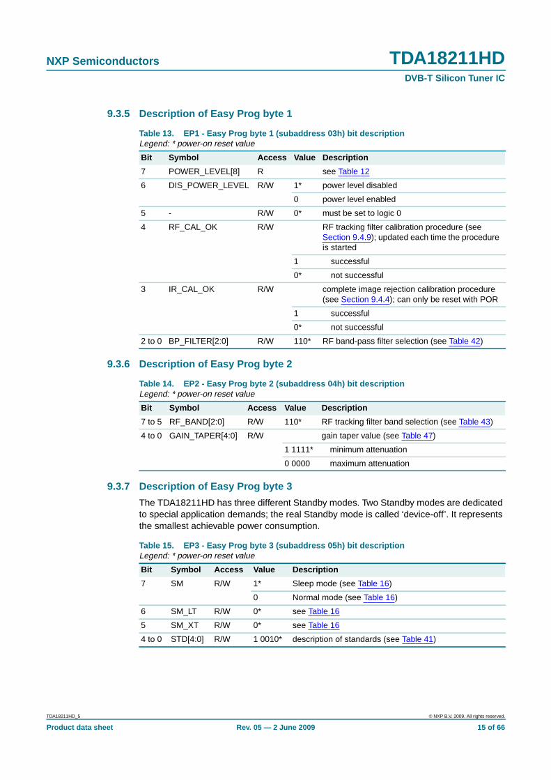
9.3.5 Description of Easy Prog byte 1
9.3.6 Description of Easy Prog byte 2
9.3.7 Description of Easy Prog byte 3
The TDA18211HD has three different Standby modes. Two Standby modes are dedicatedto special application demands; the real Standby mode is called ‘device-off’. It representsthe smallest achievable power consumption.
Table 13. EP1 - Easy Prog byte 1 (subaddress 03h) bit descriptionLegend: * power-on reset value
Bit Symbol Access Value Description
7 POWER_LEVEL[8] R see Table 12
6 DIS_POWER_LEVEL R/W 1* power level disabled
0 power level enabled
5 - R/W 0* must be set to logic 0
4 RF_CAL_OK R/W RF tracking filter calibration procedure (seeSection 9.4.9); updated each time the procedureis started
1 successful
0* not successful
3 IR_CAL_OK R/W complete image rejection calibration procedure(see Section 9.4.4); can only be reset with POR
1 successful
0* not successful
2 to 0 BP_FILTER[2:0] R/W 110* RF band-pass filter selection (see Table 42)
Table 14. EP2 - Easy Prog byte 2 (subaddress 04h) bit descriptionLegend: * power-on reset value
Bit Symbol Access Value Description
7 to 5 RF_BAND[2:0] R/W 110* RF tracking filter band selection (see Table 43)
4 to 0 GAIN_TAPER[4:0] R/W gain taper value (see Table 47)
1 1111* minimum attenuation
0 0000 maximum attenuation
Table 15. EP3 - Easy Prog byte 3 (subaddress 05h) bit descriptionLegend: * power-on reset value
Bit Symbol Access Value Description
7 SM R/W 1* Sleep mode (see Table 16)
0 Normal mode (see Table 16)
6 SM_LT R/W 0* see Table 16
5 SM_XT R/W 0* see Table 16
4 to 0 STD[4:0] R/W 1 0010* description of standards (see Table 41)
TDA18211HD_5 © NXP B.V. 2009. All rights reserved.
Product data sheet Rev. 05 — 2 June 2009 15 of 66

NXP Semiconductors TDA18211HDDVB-T Silicon Tuner IC
[1] In all modes, the I2C-bus interface remains active. All other codes are not valid.
9.3.8 Description of Easy Prog byte 4
It is recommended to follow the flowcharts described in Section 9.4 in order to performany calibration, as they require a precise set of sequential operations. The furthercomments can only give an overview of what is typically done during the flowchart.
The TDA18211HD has two calibration modes: one for the image rejection calibration, andone for the RF tracking filters calibration.
Table 16. Standby modes [1]
Bit Circuit Mode
SM SM_LT SM_XT Loop-through
Slave-tuneroutput
Crystaloscillator
0 0 0 on on on Normal mode
1 0 0 on on on Standby mode with crystaloscillator, slave-tuner output andloop-through output on
1 1 0 off off on Standby mode with only crystaloscillator and its output buffer on
1 1 1 off off off Device-off mode
Table 17. EP4 - Easy Prog byte 4 (subaddress 06h) bit descriptionLegend: * power-on reset value
Bit Symbol Access Value Description
7 FM_RFN R/W selection which input is fed to RF filter
1 FM input (RF LNA on; FM LNA on)
0* RF input (RF LNA on; FM LNA off)
6 XTOUT_ON R/W 1* 16 MHz on pins XTOUTP and XTOUTN
0 not 16 MHz on pins XTOUTP and XTOUTN
3 - R/W 1* must be set to logic 1
4 to 2 IF_LEVEL[2:0] R/W IF output level selection and attenuation with regard to2 V (p-p)
000* 2 V (p-p); 0 dB
001 1.25 V (p-p); 4 dB
010 1 V (p-p); 6 dB
011 0.8 V (p-p); 8 dB
100 not used
101 not used
110 not used
111 0.5 V (p-p); 12 dB
1 to 0 CAL_MODE[1:0] R/W calibration mode selection
00* no calibration (Normal mode)
01 Power detection mode
10 image rejection calibration (IRCAL) mode
11 RF tracking filters calibration (RFCAL) mode
TDA18211HD_5 © NXP B.V. 2009. All rights reserved.
Product data sheet Rev. 05 — 2 June 2009 16 of 66

NXP Semiconductors TDA18211HDDVB-T Silicon Tuner IC
The image rejection calibration consists in optimizing some tunable parameters inside themixer throughout a set of internal measurements, leading to ensure a 65 dB typical valueof image rejection. The internal signal used during this phase is generated by the PLLcalibration (CAL PLL).
The RF tracking filters central frequency can be adjusted with the tuning wordRFC_CPROG. The RF tracking filters calibration (RFCAL) consists of an internal tone atthe input of the tracking filters (with the CAL PLL), and finding the RFC_CPROGcorresponding to the maximum transmitted power. The RFCAL is just a little part of amore complex algorithm fully described in the flowcharts in Section 9.4.
The Power detection mode is a Normal mode where the detector used for the calibrationsis switched ON. This special mode enables to sense the power at the input of theTDA18211HD and makes the power scan algorithm possible (see Section 9.4.8“Flowchart TDA18211PowerScan”).
9.3.9 Description of Easy Prog byte 5
9.3.10 Description of Cal Post-Divider byte
9.3.11 Description of Cal divider bytes 1, 2 and 3
Table 18. EP5 - Easy Prog byte 5 (subaddress 07h) bit descriptionLegend: * power-on reset value
Bit Symbol Access Value Description
7 EXTENDED_REG R/W enables the extended register addressing
1 extended register (00h to 26h)
0* limited register (00h to 0Fh); only 1 byte canbe programmed after address 0Fh within 1transmission
6 to 4 IR_GSTEP[2:0] R/W 011* gain step for image rejection calibration
3 - R/W 0* must be set to logic 0
2 to 0 IR_MEAS[2:0] R/W 000* image rejection measurement frequency range(see Table 51)
Table 19. CPD - Cal Post-Divider byte (subaddress 08h) bit descriptionLegend: * power-on reset value
Bit Symbol Access Value Description
7 to 0 CAL_POST_DIV[7:0] R/W 00h* calibration synthesizer post-divider (seeTable 46)
Table 20. CD1, CD2 and CD3 - Cal divider bytes 1, 2 and 3 (address 09h, 0Ah and 0Bh) bitdescription
Legend: * power-on reset value
Address Register Bit Symbol Access Value Description
09h CD1 7 - R/W 0* must be set to logic 0
6 to 0 CAL_DIV[22:16] R/W 00h* calibration synthesizer maindivider bits0Ah CD2 7 to 0 CAL_DIV[15:8] R/W 00h*
0Bh CD3 7 to 0 CAL_DIV[7:0] R/W 00h*
TDA18211HD_5 © NXP B.V. 2009. All rights reserved.
Product data sheet Rev. 05 — 2 June 2009 17 of 66

NXP Semiconductors TDA18211HDDVB-T Silicon Tuner IC
9.3.12 Description of Main Post-Divider byte
9.3.13 Description of Main divider bytes 1, 2 and 3
Table 21. MPD - Main Post-Divider byte (subaddress 0Ch) bit descriptionLegend: * power-on reset value
Bit Symbol Access Value Description
7 IF_NOTCH R/W 0* adds a DC notch in IF for a betteradjacent channels rejection; dependson standards; see Table 41
6 to 4 MAIN_POST_DIV[6:4] R/W 000* LO synthesizer post-divider (seeTable 45)
3 DCDC_CKSW R/W allows switching between 16 MHz andsub-harmonic LO for DC-to-DCconverter locking
1 16 MHz
0* sub-harmonic LO
2 to 0 MAIN_POST_DIV[2:0] R/W 000* LO synthesizer post-divider (seeTable 45)
Table 22. MD1, MD2 and MD3 - Main divider bytes 1, 2 and 3 (address 0Dh, 0Eh and 0Fh) bitdescription
Legend: * power-on reset value
Address Register Bit Symbol Access Value Description
0Dh MD1 7 - R/W 0* must be set to logic 0
6 to 0 MAIN_DIV[22:16] R/W 00h* LO synthesizer main divider bits
0Eh MD2 7 to 0 MAIN_DIV[15:8] R/W 00h*
0Fh MD3 7 to 0 MAIN_DIV[7:0] R/W 00h*
TDA18211HD_5 © NXP B.V. 2009. All rights reserved.
Product data sheet Rev. 05 — 2 June 2009 18 of 66

NXP Semiconductors TDA18211HDDVB-T Silicon Tuner IC
9.3.14 Description of Extended bytes 1 to 23
Table 23. EB1 to EB23 - Extended bytes 1 to 23 (address 10h to 26h) bit descriptionLegend: * power-on reset value
Address Register Bit Symbol Access Value Description
10h EB1 7 to 3 EB1[7:3] R 1 1111* extended byte 1
2 CALVCO_FORLON R determines VCO used during Normalmode operations
1* LO VCO is used
0 CAL VCO is used
1 AGC1_ALWAYS_MASTERN
R enables AGC1 normal operationwhatever the tuner type, master orslave.
1* normal operation for the master;6 dB fixed for the slave
0 normal operation for both the masterand the slave
0 AGC1_FIRSTN R determines which AGC will be updatedwhen detectors 1 and 2 are up
1* AGC1 and AGC2 both updated
0 AGC1 has priority on AGC2
11h EB2 7 to 0 EB2[7:0] R/W 0000 0001* extended byte 2
12h EB3 7 to 0 EB3[7:0] R/W 1000 0100* extended byte 3
13h EB4 7 to 6 EB4[7:6] R/W 01* extended byte 4
5 LO_FORCESRCE R/W 1 forces the main PLL charge pump tosource current to the main PLL loopfilter
0* no force
4 to 0 EB4[4:0] R/W 0 0001* extended byte 4
14h EB5 7 and 6 EB5[7:0] R/W 0000 0001* extended byte 5
15h EB6 7 to 0 EB6[7:0] R/W 1000 0100* extended byte 6
16h EB7 7 and 6 EB7[7:6] R/W 01* extended byte 7
5 CAL_FORCESRCE R/W 1 forces the main PLL charge pump tosource current to the main PLL loopfilter
0* no force
4 to 0 EB7[4:0] R/W 0 1000* extended byte 7
17h EB8 7 CID_ALARM R signal sensed by the power detectorused during calibrations
1 out of range
0* in range
6 to 4 EB8[6:4] R/W 111* extended byte 8
3 EB8[3] R 0*
2 to 0 EB8[2:0] R/W 101*
18h EB9 7 to 0 EB9[7:0] W 0000 0000* extended byte 9
19h EB10 7 and 6 EB10[7:6] R XX extended byte 10
5 to 0 CID_GAIN[5:0] R XX XXXX calibration power detector output
TDA18211HD_5 © NXP B.V. 2009. All rights reserved.
Product data sheet Rev. 05 — 2 June 2009 19 of 66

NXP Semiconductors TDA18211HDDVB-T Silicon Tuner IC
1Ah EB11 7 to 0 EB11[7:0] R/W 1000 0110* extended byte 11
1Bh EB12 7 and 6 EB12[7:6] R 00* extended byte 12
5 PD_AGC1_DET R/W AGC1 detector
1 power-down
0* no power-down
4 PD_AGC2_DET R/W AGC2 detector
1 power-down
0* no power-down
3 to 0 EB12[3:0] R/W 0111* extended byte 12
1Ch EB13 7 EB13[7] R/W 1* extended byte 13
6 to 4 RFC_K[2:0] R/W 100* parameters used during the RFtracking filters calibration (seeTable 44)
3 and 2 RFC_M[1:0] R/W 00*
1 to 0 EB13[1:0] R/W 10* extended byte 13
1Dh EB14 7 to 0 RFC_CPROG[7:0] R/W 0000 0000* tuning word of the RF tracking filters
1Eh EB15 7 to 4 EB15[7:4] R/W 1000* extended byte 15
3 to 0 EB15[3:0] R XXXX*
1Fh EB16 7 to 0 EB16[7:0] W 000X XX00* extended byte 16
20h EB17 7 to 0 EB17[7:0] W 000X XXXX* extended byte 17
21h EB18 7 AGC1_LOOP_OFF R/W turns the AGC1 loop
1 off
0* on
6 to 2 EB18[6:2] R/W 000 00* extended byte 18
1 and 0 AGC1_GAIN[1:0] R/W AGC1 gain
00* 6 dB
01 9 dB
10 12 dB
11 15 dB
22h EB19 7 to 0 EB19[7:0] W 000X XX00* extended byte 19
23h EB20 7 and 6 EB20[7:6] W 10* extended byte 20
5 FORCE_LOCK W forces the internal lock indicator
1 forced to logic 1
0* not forced
4 to 0 EB20[4:0] W X XXXX* extended byte 20
Table 23. EB1 to EB23 - Extended bytes 1 to 23 (address 10h to 26h) bit description …continuedLegend: * power-on reset value
Address Register Bit Symbol Access Value Description
TDA18211HD_5 © NXP B.V. 2009. All rights reserved.
Product data sheet Rev. 05 — 2 June 2009 20 of 66

NXP Semiconductors TDA18211HDDVB-T Silicon Tuner IC
24h EB21 7 AGC2_LOOP_OFF R/W turns the AGC2 loop
1 off
0* on
6 to 2 EB21[6:2] R/W 0 1100* extended byte 21
1 and 0 AGC2_GAIN[1:0] R/W AGC2 gain
00 −15 dB
01 −12 dB
10 −9 dB
11* −6 dB
25h EB22 7 EB22[7] R 0* extended byte 22
6 to 4 RFAGC_TOP[2:0] R/W 100* take over point of the RF AGC,detection in RF
3 to 0 IFAGC_TOP[3:0] R/W 1000* take over point of the RF AGC,detection in IF
26h EB23 7 to 3 EB23[7:3] R/W 1 0110* extended byte 23
2 FORCELP_FC2_EN
R/W 0* 1.5 MHz bandwidth filter selection; seeTable 24
1 LP_FC[2] R/W 0*
0 EB23[0] R/W 0* extended byte 23
Table 23. EB1 to EB23 - Extended bytes 1 to 23 (address 10h to 26h) bit description …continuedLegend: * power-on reset value
Address Register Bit Symbol Access Value Description
Table 24. Low pass cut-off frequency
FORCELP_FC2_EN LP_FC[2] STD[1:0] Cut-off frequency (MHz)
0 X 00 6
0 X 01 7
0 X 10 8
0 X 11 9
TDA18211HD_5 © NXP B.V. 2009. All rights reserved.
Product data sheet Rev. 05 — 2 June 2009 21 of 66

NXP Semiconductors TDA18211HDDVB-T Silicon Tuner IC
9.4 I2C-bus programming flowchartsThe following flowcharts describe how to:
• Initialize the TDA18211HD
• Launch the calibrations
• Go to Normal mode
The image rejection calibration as well as RF tracking filters calibration must be launchedthe way explicitly described in the flowchart. If not done this way, it may result in badcalibration or even blocking the TDA18211HD, which makes it impossible to communicatevia the I2C-bus.
For proper internal initialization, switching to Normal mode also requires a single I2C-bussequence from subaddresses 03h to 0Fh.
9.4.1 Flowchart explanation
This section provides instructions for reading the flowcharts.
1. I2C-bus write:
– IR_GSTEP is updated, no immediate I2C-bus write
– I2C_XTOUT_ASYM is updated followed by an I2C-bus write of EP5
– PD_AGC1_DET is updated followed by an I2C-bus write of EB12
– I2C-bus write of EB13 with current value of the software internal table of EB13
I2C-bus read:
– Sub-addressing is not supported in read mode
– The only recommended I2C-bus read access procedures of the TDA18211HD aredescribed in Section 9.4.16 “Flowchart TDA18211Read” and Section 9.4.17“Flowchart TDA18211ReadExtended”
Fig 3. Programming sequence
001aag935
initialization phase
actions registers to updatein the softwareinternal table
tuner registersupdate
master or slavefor I2C-bus write
IR_GSTEP = 2hI2C_XTOUT_ASYM = 1PD_AGC1_DET = 1-
-EP5EB12EB13
IR_GSTEP = 2h,I2C_XTOUT_ASYM = 1,PD_AGC1_DET = 1
-
- EP5EB12EB13
- EP1...EP2,MD3
- EP1...CD2
Internal table I2C-bus
MS
TDA18211HD_5 © NXP B.V. 2009. All rights reserved.
Product data sheet Rev. 05 — 2 June 2009 22 of 66

NXP Semiconductors TDA18211HDDVB-T Silicon Tuner IC
2. Update at the same moment is indicated by separation with commas:
IR_GSTEP, I2C_XTOUT_ASYM and PD_AGC1_DET are updated, no I2C-busregisters update
3. I2C-bus registers update of the bytes EP5, EB12 and EB13
4. Bytes EP1 to CD2 are written in a single I2C-bus sequence
Example:
Start C0 03 EP1 EP2 EP3 EP4 EP5 CPD CD1 CD2 Stop
5. Bytes EP1, EP2 and MD3 are written in as many I2C-bus sequences as needed
Example:
Start C0 03 EP1 EP2 Stop
Start C0 0F MD3 Stop
Fig 4. Blocks used in the flowcharts
Master/slave variable MS_init is input for each of the three procedures.
Fig 5. Variable used in multiple procedures
XX
XX
XX 001aag722
XX
stored or already calculated data
input variable
result of an operation
output variable
001aag936
I2C initialization sequenceCall TDA18211FixedContentsI2Cupdate
Calibrate the RF tracking filterscall TDA18211CalcRFFilterCurve
Back to PORCall TDA18211MSPOR
MS_init
TDA18211HD_5 © NXP B.V. 2009. All rights reserved.
Product data sheet Rev. 05 — 2 June 2009 23 of 66

NXP Semiconductors TDA18211HDDVB-T Silicon Tuner IC
Units
• In the flowcharts, hexadecimal values end with “h”, decimal values with “d”
• Frequency variables used in computations are expressed in kHz, for example 1 GHzis written as 1000000.
xx is a list of values stored in the first column of the map XY_map.
yy is a list of values stored in column in XY_map.
yy_out is the particular value of yy to find row n. xx(n − 1) < xx_in ≤ xx(n).
a. General description to find a value in a table
Finding the row of RFC_K: 350000 < 650000 ≤ 720000. Result n = 1. The value of RFC_K is then3 (see Table 44).
b. Example to find the value RFC_K corresponding to fRF = 650 MHz in the KM_map.
Fig 6. Finding a value in a table
001aag822
xx_inXY_map
yy_outFind yy = f(xx) in XY_map
001aag723
650 MHzKM_map
RFC_KFind RFC_K = fRF(max) inKM_map
TDA18211HD_5 © NXP B.V. 2009. All rights reserved.
Product data sheet Rev. 05 — 2 June 2009 24 of 66

NXP Semiconductors TDA18211HDDVB-T Silicon Tuner IC
9.4.2 Flowchart TDA18211SetRf_dual
The initialization phase has to be launched before any SetRf.
MS = 1: master is selected for the channel configuration.
MS = 0: slave is selected for the channel configuration.
Table 25. TDA18211SetRf_dual
Function Description Reference
Description protocol top view for a dual-tuner application
Input RF_freq, Standard (from microcontroller), MS (frommicrocontroller)
Table -
Output -
Fig 7. Flowchart TDA18211SetRf_dual
001aag937
Master and slave initializationCall TDA18211InitCal
Set the RF tracking filtersCall TDA18211RFtrackingFiltersCorrection
Set the tuner to the wanted channelCall TDA18211ChannelConfiguration
TMVALUE_RFCAL
TMVALUE_RFCALinit_done
StartTDA18211SetRf_dual
EndTDA18211SetRf_dual
init_done = 1
StandardRF_freqMS
RF_freqMS
No
Yes
TDA18211HD_5 © NXP B.V. 2009. All rights reserved.
Product data sheet Rev. 05 — 2 June 2009 25 of 66

NXP Semiconductors TDA18211HDDVB-T Silicon Tuner IC
9.4.3 Flowchart TDA18211InitCal
Table 26. TDA18211InitCal
Function Description Reference
Description systematic initialization for master and slave tuners
Input MS_init
Table -
Output TMVALUE_RFCAL, init_done
Fig 8. Flowchart TDA18211InitCal
001aag938
MS_init = 1
Master initialization
I2C initialization sequenceCall TDA18211FixedContentsI2Cupdate
Calibrate the RF tracking filtersCall TDA18211CalcRFFilterCurve
Back to PORCall TDA18211MSPOR
MS_init
MS_init
init_done
TMVALUE_RFCAL
StartTDA18211InitCal
EndTDA18211InitCal
MS_init = 0
Slave initialization
I2C initialization sequenceCall TDA18211FixedContentsI2Cupdate
Calibrate the RF tracking filtersCall TDA18211CalcRFFilterCurve
Back to PORCall TDA18211MSPOR
init_done = true
MS_init
MS_init
TDA18211HD_5 © NXP B.V. 2009. All rights reserved.
Product data sheet Rev. 05 — 2 June 2009 26 of 66

NXP Semiconductors TDA18211HDDVB-T Silicon Tuner IC
9.4.4 Flowchart TDA18211FixedContentsI2Cupdate
Table 27. TDA18211FixedContentsI2Cupdate
Function Description Reference
Description update and write the TDA18211HD registers,sequential update of AGC1 and AGC2,image calibration algorithm
Input MS
Table -
Output -
Fig 9. Flowchart TDA18211FixedContentsI2Cupdate
001aag939
Actions
Internal table update withcorrect values
Tuner registers update
TM = 08hPL = 80hEP1 = C6hEP2 = DFhEP3 = 16hEP4 = 60hEP5 = 80hCPD = 80hCD1 = 00hCD2 = 00hCD3 = 00hMPD = 00hMD1 = 00hMD2 = 00hMD3 = 00hEB1 = FChEB2 = 01hEB3 = 84hEB4 = 41hEB5 = 01hEB6 = 84hEB7 = 40hEB8 = 07hEB9 = 00hEB10 = 00hEB11 = 96hEB12 = 33hEB13 = C1hEB14 = 00hEB15 = 8FhEB16 = 00hEB17 = 00hEB18 = 8ChEB19 = 00hEB20 = 20hEB21 = B3hEB22 = 48hEB23 = B0h
--------------------------------------
Internal table
IRCAL low bandInitialization
EP3 = 1FhEP4 = 66hEP5 = 81hCPD = CChCD1 = 6ChCD2 = 00hCD3 = 00hMPD = CDhMD1 = 77hMD2 = 08hMD3 = 00h
-----------
CALPLL update EP5 = 85hCPD = CBhCD1 = 66hCD2 = 70h
----
AGC1 gain setup EB17 = 00hEB17 = 03hEB17 = 43hEB17 = 4Ch
EB17EB17EB17EB17
I2C-bus
- TM...EB23
Tuner registers update - EP3...MD3
MAIN PLL CP source on EB4 = 61h EB4
Tuner registers update - EP3...CD3
EP2
Launch detector -
Launch optimization algorithm -
EP1
Wait 5 ms - PLL locking
MAIN PLL CP source off EB4 = 41h EB4
Wait 1 ms
Wait 5 ms - PLL locking
Wait 30 ms - optimization
Wait 5 ms - measurement
IRCAL high bandInitialization
EP5 = 83hCPD = 98hCD1 = 65hCD2 = 00hMPD = 99hMD1 = 71hMD2 = CDh
-------
CALPLL update EP5 = 87hCD1 = 65hCD2 = 50h
---
Tuner registers update - EP3...MD3
Tuner registers update - EP3...CD3
EP2
Launch detector -
Launch optimization algorithm -
EP4Back to normal mode EP4 = 64h
EP1Synchronization -
EP1
Wait 5 ms - PLL locking
Wait 5 ms - PLL locking
Wait 30 ms - optimization
Wait 5 ms - measurement
IRCAL mid bandInitialization
EP5 = 82hCPD = A8hCD2 = 00hMPD = A9hMD1 = 73hMD2 = 1Ah
------
CALPLL update EP5 = 86hCPD = A8hCD1 = 66hCD2 = A0h
----
Tuner registers update - EP3...MD3
Tuner registers update - EP3...CD3
EP2
Launch detector -
Launch optimization algorithm -
EP1
Wait 5 ms - PLL locking
Wait 5 ms - PLL locking
Wait 30 ms - optimization
Wait 5 ms - measurement
StartTDA18211FixedContentsI2Cupdate
EndTDA18211FixedContentsI2Cupdate
MS
TDA18211HD_5 © NXP B.V. 2009. All rights reserved.
Product data sheet Rev. 05 — 2 June 2009 27 of 66

NXP Semiconductors TDA18211HDDVB-T Silicon Tuner IC
9.4.5 Flowchart TDA18211CalcRFFilterCurve
Table 28. TDA18211CalcRFFilterCurve
Function Description Reference
Description calculate the RF filter curves coefficients
Input RF1_default, RF2_default, RF3_default, MS
Table RF_BAND_map Table 43 “RF_BAND_map”
Output TMVALUE_RFCAL
Fig 10. Flowchart TDA18211CalcRFFilterCurve
001aag940
Wait 200 ms for die temperature stabilization
fRF(max) = 203500
PowerScan InitializationCall TDA18211PowerScanInit
Read die current temperatureCall TDA18211ThermometerRead
RF_Band 4 filters calibrationCall TDA18211RFTrackingFiltersInit
fRF(max) = 457800
RF_Band 5 filters calibrationCall TDA18211RFTrackingFiltersInit
fRF(max) = 865000
RF_Band 6 filters calibrationCall TDA18211RFTrackingFiltersInit
fRF(max)
RF1_4, RF_A1_4,RF_B1_4
fRF(max)
RF1_5, RF_B1_5, RF2_5, RF_A1_5,RF3_5, RF_A2_5, RF_B2_5
fRF(max)
RF1_6, RF_B1_6, RF2_6, RF_A1_6,RF3_6, RF_A2_6, RF_B2_6
MS
TMVALUE_RFCAL
StartTDA18211CalcRFFilterCurve
EndTDA18211CalcRFFilterCurve
fRF(max)
fRF(max)
fRF(max)
TDA18211HD_5 © NXP B.V. 2009. All rights reserved.
Product data sheet Rev. 05 — 2 June 2009 28 of 66

NXP Semiconductors TDA18211HDDVB-T Silicon Tuner IC
9.4.6 Flowchart TDA18211RFTrackingFiltersInit
bcal is a boolean output from TDA18211PowerScan:
bcal = 1 (true): enables the calibration of the RF tracking filters
bcal = 0 (false): no calibration is performed, default values for RFC_CPROG are used
Table 29. TDA18211RFTrackingFiltersInit
Function Description Reference
Description calculate the RF filter curve coefficients used fortheir approximation
Input fRF(max), MS
Table RF_CAL_map (Cprog_table = f(frequency)) Table 49 “RF_CAL_map”
Output RF1, RF2, RF3, RF_A1, RF_B1, RF_B2
TDA18211HD_5 © NXP B.V. 2009. All rights reserved.
Product data sheet Rev. 05 — 2 June 2009 29 of 66

NXP Semiconductors TDA18211HDDVB-T Silicon Tuner IC
Fig 11. Flowchart TDA18211RFTrackingFiltersInit
001aag941
Look for optimized calibration frequencyCall TDA18211PowerScan
RF_A1 = 0, RF_B1 = 0, RF_A2 = 0, RF_B2 = 0
Find Cprog_table = fRF(max) in RF_CAL_map
Find RF1_default, RF2_default, RF3_default = fRF(max) in RF_BAND_mapRF1_default
RF1_default,RF2_default,RF3_default
Cprog_table1
bcalRF1
StartTDA18211RFTrackingFiltersInit
EndTDA18211 RFTrackingFiltersInit
bcal = 1
MS
RF1
RF_B1RF_A1
No
Yes
bcal = 0No
Yes
RF2_default = 0Yes
No
Look for optimized calibration frequencyCall TDA18211PowerScan
RF2_default
bcalRF2
MS
RF2
Find Cprog_cal1 to track RF1Call TDA18211CalibrateRF
RF1
RF1RF_CAL_map
Cprog_cal1 = Cprog_table1 Cprog_cal1Cprog_table1
RF_B1 = Cprog_cal1 − Cprog_table1RF1Cprog_cal1Cprog_table1
Cprog_cal1
MS
Find Cprog_table = fRF(max) in RF_CAL_map Cprog_table2
EndTDA18211 RFTrackingFiltersInit
bcal = 1
RF_A1
No
Yes
bcal = 0No
Yes
RF3_default = 0Yes
Find Cprog_cal2 to track RF2Call TDA18211CalibrateRF
RF2
RF2RF_CAL_map
Cprog_cal2 = Cprog_table2 Cprog_cal2
RF_A1 = (Cprog_cal2 − Cprog_table2 − Cprog_cal1 + Cprog_table1)/(RF2 − RF1)
RF1RF2Cprog_cal1Cprog_cal2Cprog_table1Cprog_table2
RF_A2RF_B2RF_A2 = (Cprog_cal3 − Cprog_table3 − Cprog_cal2 + Cprog_table2)/(RF3 − RF2)
RF_B2 = Cprog_cal2 − Cprog_table2
RF2RF3Cprog_cal2Cprog_cal3Cprog_table2Cprog_table3
Cprog_cal2
MS
No
Look for optimized calibration frequencyCall TDA18211PowerScan
RF3_default
bcalRF3
MS
RF3
Find Cprog_table = fRF(max) in RF_CAL_map Cprog_table3
EndTDA18211RFTrackingFiltersInit
bcal = 1No
Yes
bcal = 0No
Yes
Find Cprog_cal3 to track RF3Call TDA18211CalibrateRF
RF3
RF3RF_CAL_map
Cprog_cal3 = Cprog_table3 Cprog_cal3Cprog_table3
Cprog_cal3
MS
Cprog_table2
TDA18211HD_5 © NXP B.V. 2009. All rights reserved.
Product data sheet Rev. 05 — 2 June 2009 30 of 66

NXP Semiconductors TDA18211HDDVB-T Silicon Tuner IC
9.4.7 Flowchart TDA18211PowerScanInit
9.4.8 Flowchart TDA18211PowerScan
Table 30. TDA18211PowerScanInit
Function Description Reference
Description fixed settings of the TDA18211PowerScan
Input MS
Table
Output
Fig 12. Flowchart TDA18211PowerScanInit
001aag942
StartTDA18211PowerScanInit
EndTDA18211PowerScanInit
MS
STD = 12,IF_LEVEL = 0CAL_MODE = 0
-
Actions
Set standard mode to digital mode
- EP3...EP4Tuner registers update
Internal table I2C-bus
AGC1_GAIN = 0AGC2_GAIN = 0
EB18-
Set AGC1_GAIN to 6 dBSet AGC2_GAIN to −15 dB
FORCELP_FC2_EN = 1,LP_FC[2] = 1
-1.5 MHz low-pass filter
- EB21...EB23Tuner register update
Table 31. TDA18211PowerScan
Function Description Reference
Description find an interferer free calibration frequency
Input freq_input, MS
Table RF_BAND_map,
RF_CAL_map,
CID_TARGET_map
Table 43 “RF_BAND_map”
Table 49 “RF_CAL_map”
Table 52 “CID_TARGET_map”
Output bcal, freq_output
TDA18211HD_5 © NXP B.V. 2009. All rights reserved.
Product data sheet Rev. 05 — 2 June 2009 31 of 66

NXP Semiconductors TDA18211HDDVB-T Silicon Tuner IC
Fig 13. Flowchart TDA18211PowerScan
001aag943
CID_GAIN < CID_Target
CID_Targetcount_limit
freq_MAINPLL
MS
freq_input
freq_input
freq_input
MS
bcalfreq_output
StartTDA18211PowerScan
EndTDA18211PowerScan
RF_BAND_mapRF_CAL_mapCID_TARGET_map
freq_MAINPLL
count
freq_MAINPLL
sgn count
freq_MAINPLL
RF_BAND = RF_BANDRFC_CPROG = CPROG_tableGAIN_TAPER = GAIN_TAPERCID_Target = CID_Targetcount_limit = count_limit
-
Actions
freq_MAINPLL
freq_MAINPLL = freq_input + 1 MHz
count
CID_GAIN
wait
count = count + 200d
CID_GAINRead power detection informationsCall TDA18211ReadExtended
sgncountwait
sgn = − sgncount = 200dwait = true
bcal = 1freq_output = freq_MAINPLL − 1 MHz
EndTDA18211PowerScan
bcalfreq_outputfreq_input
bcal = 0 freq_output = freq_input
sgnfreq_outputbcalcountwait
Algorrithm Initializationsgn =1freq_output = freq_inputbcal = 0count = 0wait = false
freq_MAINPLL = freq_input + sgn × count + 1 MHz
Wait 100 µs - PLL lockingWait 5 ms - PLL locking
wait = false
Downconvert updated freq_input to 1 MHzCall TDA18211CalcMAINPLL
Read power detection informationsCall TDA18211ReadExtended
No
No
Yes
Yes
Wait 5 ms - PLL locking
Downconvert freq_input to 1 MHzCall TDA18211CalcMAINPLL
Find RF_BAND = fRF(max) in RF_BAND_map(MS)Find Cprog_table = fRF(max) in RF_CAL_mapFind GAIN_TAPER = fRF(max) in GAIN_TAPER_mapFind CID_TARGET count_limit = fRF(max) inCID_TARGET_map
- EP2, EB14Tuner register update
Internal table PC
Detection modeLaunch power detection measurement
CAL_MODE = 1-
EP4EP2
Launch power detection measurement - EP2
count > count_limitNo
No
Yes
Yes
Yes
CID_GAIN ≥ CID_Target
wait = true
No sgn > 0
TDA18211HD_5 © NXP B.V. 2009. All rights reserved.
Product data sheet Rev. 05 — 2 June 2009 32 of 66

NXP Semiconductors TDA18211HDDVB-T Silicon Tuner IC
9.4.9 Flowchart TDA18211CalibrateRF
Table 32. TDA18211CalibrateRF
Function Description Reference
Description find the Cprog for which freq_input isthe central frequency of the RF trackingfilters
Input freq_input, MS
Table BP_FILTER_map,
KM_map,
GAIN_TAPER_map
Table 42 “BP_FILTER_map”
Table 44 “KM_map”
Table 47 “GAIN_TAPER_map”
Output RFC_CPROG
TDA18211HD_5 © NXP B.V. 2009. All rights reserved.
Product data sheet Rev. 05 — 2 June 2009 33 of 66

NXP Semiconductors TDA18211HDDVB-T Silicon Tuner IC
Fig 14. Flowchart TDA18211CalibrateRF
001aag944
CAL_MODE = 0SM_LT = 1AGC1_GAIN = 3h
EP4-EB18
Actions
Normal modeSwitch OFF AGC1Set AGC1_GAIN to 15 dB
BP_FILTER = BP_FILTERGAIN_TAPER = GAIN_TAPERRF_BAND = RF_BANDRFC_K = RFC_K, RFC_M = RFC_M
----
Frequency dependent parameters updateFind BP_FILTER = fRF(max) in BP_FILTER_mapFind GAIN_TAPER = fRF(max) in GAIN_TAPER_mapFind RF_BAND = fRF(max) in RF_BAND_mapFind RFC_K, RFC_M = fRF(max) in KM_map
Internal table I2C-bus
RFC_CPROG
BP_FILTER_mapKM_mapGAIN_TAPER_map
freq_inputMS
freq_input
MS
freq_input + 1 MHz
- EP1 … EP2, EB13Tuner registers update
- EP4 … EP5Tuner registers update
Set the internal calibration signalCall TDA18211CalcCALPLL
Normal operation for the MAIN PLL charge pumpNormal operation for the CAL PLL charge pump
Get the calibration resultCall TDA18211ReadExtended
LO_FORCESRCE = 0CAL_FORCESRCE = 0
Downconvert the calibration signal to 1 MHzCall TDA18211CalcMAINPLL
Wait 5 ms
Wait 10 ms - PLLs locking
Internal synchronization EP2, EP1, EP2, EP1
EB4EB7
Launch the RF Tracking filters calibration FORCE_LOCK = 1
Wait 60 ms - calibration on going
EB20
Normal modeSwitch ON AGC1Set AGC1_GAIN to 6 dB
CAL_MODE = 0SM_LT = 0AGC1_GAIN = 0
Tuner registers update
Synchronization
--EB18
- EP3 ... 4
- EP1
LO_FORCESRCE = 1CAL_FORCESRCE = 1RFC_CPROG = 0FORCE_LOCK = 0CAL_MODE = 3h
EB4EB7EB14EB20-
MAIN PLL charge pump sourceCAL PLL charge pump sourceForce DCDC converter to 0 VDisable PLLs lockRF tracking filters calibration mode
Start TDA18211CalibrateRF
End TDA18211CalibrateRF
TDA18211HD_5 © NXP B.V. 2009. All rights reserved.
Product data sheet Rev. 05 — 2 June 2009 34 of 66

NXP Semiconductors TDA18211HDDVB-T Silicon Tuner IC
9.4.10 Flowchart TDA18211MSPOR
9.4.11 Flowchart TDA18211RFtrackingFiltersCorrection
Table 33. TDA18211MSPOR
Function Description Reference
Description master or slave tuner goes to Power-On Reset(POR) mode
Input MS
Table -
Output -
Fig 15. Flowchart TDA18211MSPOR
001aag945
StartTDA18211MSPOR
EndTDA18211MSPOR
MS
PD_AGC1_DET = 0AGC1_LOOP_OFF = 0AGC1_GAIN = 0AGC2_GAIN = 3h
EB12-EB18-
Actions
Power up Detector 1Turn AGC1 loop ONSet AGC1_GAIN to 6 dBSet AGC2_GAIN to −6 dB
SM = 1, SM_LT = 0,SM_XT = 0 EP3
POR mode
Internal table I2C-bus
FORCELP_FC2_EN = 0,LP_FC[2] = 0 EB21 ... EB23
1.5 MHz low-pass filter disabled
Table 34. TDA18211RFtrackingFiltersCorrection
Function Description Reference
Description find the Cprog corresponding to theprogrammed central frequencyfreq_input
Input freq_input, TMVALUE_RFCAL, MS
Table RF_BAND_map,
RF_CAL_OVER_DT_map,
RF_CAL_map
Table 43 “RF_BAND_map”
Table 48 “RF_CAL_DC_OVER_DT_map”
Table 49 “RF_CAL_map”
Output -
TDA18211HD_5 © NXP B.V. 2009. All rights reserved.
Product data sheet Rev. 05 — 2 June 2009 35 of 66

NXP Semiconductors TDA18211HDDVB-T Silicon Tuner IC
Fig 16. Flowchart TDA18211RFtrackingFiltersCorrection
001aag946
Action
Power up TDA18211 SM = 0, SM_LT = 0,SM_XT = 0
EP3
Read die current temperatureCall TDA18211ThermometerRead
Frequency dependant parameters updateFind RFC_CPROG = fRF(max) in RF_CAL_map, Cprog_table = RFC_CPROGFind RF1, RF2, RF3, RF_A1, RF_A2, RF_B1, RF_B2 = fRF(max) in RF_BAND_map(MS)
Internal table I2C-bus
Calculate final CprogCprog = Capprox + RFCAL_TCOMP
RFC_CPROG = Cprog EB14
RF_CAL_mapRF_BAND_map
TMVALUE_CURRENT
Find dCoverdT = fRF(max) in RF_CAL_DC_OVER_DT_map dCoverdT
Cprog_tableRF1RF2RF3RF_A1RF_A2RF_B1RF_B2
Start TDA18211RFTrackingFiltersCorrection
End TDA18211RFTrackingFiltersCorrection
RF3 = 0 orfreq_input < RF2
Capprox < 0 Capprox > 255
no
no no
yes
yes yes
freq_inputMS
MS
RF_CAL_DC_OVER_DT_map
freq_input
Calculate temperature compensationRFCAL_TCOMP = dCoverdT × (TMVALUE_CURRENT−TMVALUE_RFCAL) / 1000 RFCAL_TCOMPdCoverdT
TMVALUE_CURRENT
CapproxRFCAL_TCOMP
TMVALUE_RFCAL
Capprox =RF_A2 × (freq_input − RF2) +RF_B2 + Cprog_table
Capprox
RF_A2RF2RF_B2Cprog_table
freq_input
Capprox =RF_A1 × (freq_input − RF1) +RF_B1 + Cprog_table
Capprox = 255Capprox = 0
Capprox
RF_A1RF1RF_B1Cprog_table
freq_input
TDA18211HD_5 © NXP B.V. 2009. All rights reserved.
Product data sheet Rev. 05 — 2 June 2009 36 of 66

NXP Semiconductors TDA18211HDDVB-T Silicon Tuner IC
9.4.12 Flowchart TDA18211ChannelConfiguration
Table 35. TDA18211ChannelConfiguration
Function Description Reference
Description tune the tuner according to thechannel and broadcast configuration
Input freq_input, MS, Standard
Table STANDARD_DESCRIPTION_map,
BP_FILTER_map,
RF_BAND_map,
CAL_PLL_map,
GAIN_TAPER_map,
IR_MEAS_map
Table 41 “STANDARD_DESCRIPTION_map”
Table 42 “BP_FILTER_map”
Table 43 “RF_BAND_map”
Table 46 “CAL_PLL_map”
Table 47 “GAIN_TAPER_map”
Table 51 “IR_MEAS_map”
Output -
TDA18211HD_5 © NXP B.V. 2009. All rights reserved.
Product data sheet Rev. 05 — 2 June 2009 37 of 66

xxxxxxxxxxxxxxxxxxxxx xxxxxxxxxxxxxxxxxxxxxxxxxx xxxxxxx x x x xxxxxxxxxxxxxxxxxxxxxxxxxxxxxx xxxxxxxxxxxxxxxxxxx xx xxxxxxx xxxxxxxxxxxxxxxxxxxxxxxxxxx xxxxxxxxxxxxxxxxxxx xxxxxx xxxxxxxxxxxxxxxxxxxxxxxxxxxxxxxxxxx xxxxxxxxxxxx x xxxxxxxxxxxxxxxxxxxxxx xxxxxxxxxxxxxxxxxxxxxxxxxxxxxx xxxxx xxxxxxxxxxxxxxxxxxxxxxxxxxxxxxxxxxxxxxxxxxxxxxxxxx xxxxxxxxxxxxxxxxxxxxxxxxxxxxxxxxx xxxxxxxxxxxxxxxxxxxx xxx
TD
A18211H
D_5
Product data shee
NX
P S
emiconductors
TD
A18211H
DD
VB
-T S
ilicon Tuner IC
001aag947
Standard mode updatelue
Standardo Standard
tandard
----EB22-
Actions Internal table I2C-bus
-
-
Start TDA18211ChannelConfiguration MS
EB1
-
= CAL_POST_DIV && 7Fh MPD
FORCESRCE = 1
FORCESRCE = 0
TM ... EP5
EB5
EB5
[2] = 1 EP3
IF_freq
© N
XP
B.V. 2009. A
ll rights reserved.
tR
ev. 05 — 2 June 2009
38 of 66
Fig 17. Flowchart TDA18211ChannelConfiguration
Update TV broadcast parametersSwitch RFAGC to high speed modeNormal modeUpdate IF output levelUpdate IF notch frequencyUpdate extended byte 22Update IF center frequency
STD = STD from STANDARD_DESCRIPTION_map according to Standard vaSTD[2] = 0CAL_MODE = 0IF_LEVEL = IF_LEVEL from STANDARD_DESCRIPTION_map according to IF_NOTCH = IF_NOTCH from STANDARD_DESCRIPTION_map according tEB22 = EB22 from STANDARD_DESCRIPTION_map according to StandardIF_FREQ = IF_FREQ from STANDARD_DESCRIPTION_map according to S
Update frequency dependent parametersFind IR_MEAS = fRF(max) in IR_MEAS_mapFind BP_FILTER = fRF(max) in BP_FILTER_mapFind RF_BAND = fRF(max) in RF_BAND_mapFind GAIN_TAPER = fRF(max) in GAIN_TAPER_map
IR_MEAS = IR_MEASBP_FILTER = BP_FILTERRF_BAND = RF_BANDGAIN_TAPER = GAIN_TAPER
Disable power level indicator DIS_POWER_LEVEL = 1
End TDA18211ChannelConfiguration
IR_MEAS_mapBP_FILTER_mapRF_BAND_mapGAIN_TAPER_map
freq_inputMS
STANDARD_DESCRIPTION_map
Standard
Dual-tuner and AGC1 extra configurations managingMAIN VCO when Master, CAL VCO when SlaveAGC1 always activeAGC1 has priority on AGC2
Tuner registers update
freq_pll = freq_input + IF_freq
Tune to wanted channel frequencyCall TDA18211CalcMAINPLL
Tuner registers update
MAIN PLL charge pump source
Wait 1 ms
Normal operation for the MAIN PLL
- TM ... EP5
LO_FORCESRCE = 1
LO_FORCESRCE = 0
EB4
EB4
Switch RFAGC to normal speed mode STD[2] = 1 EP3
Wait 20 ms
-
CALVCO_FORLON = MSAGC1_ALWAYS_MASTERN = 0AGC_FIRSTN = 0
IF_freq
freq_pll
Tune to wanted channel frequencyCall TDA18211CalcCALPLL
Find CAL_POST_DIV = fLO(max) inCAL_PLL_map
CAL PLL charge pump source
Wait 1 ms
Normal operation for the CAL PLL
MPD
CAL_
CAL_
Tuner registers update -
Switch RFAGC to normal speed mode STD
Wait 20 ms
freq_pll
CAL_PLL_mapfreq_pll
MS
freq_input
End TDA18211ChannelConfiguration
MS = 1yes no

NXP Semiconductors TDA18211HDDVB-T Silicon Tuner IC
9.4.13 Flowchart TDA18211CalcMAINPLL
MPD, MD1, MD2 and MD3 are 8-bit registers. Arithmetical and logical operationsperformed on those registers are considered binary operations. (Dividing is right shiftingand multiplying is left shifting, etc.)
Table 36. TDA18211CalcMAINPLL
Function Description Reference
Description find the correct values for the bytesMPD, MD1, MD2, MD3 and update thetuner registers
Input freq_input, MS
Table MAIN_PLL_map Table 45 “MAIN_PLL_map”
Output -
Fig 18. Flowchart TDA18211CalcMAINPLL
001aag948
Tuner registers update
Internal table I2C-bus
Start TDA18211CalcMAINPLL
End TDA18211CalcMAINPLL
Div
MAIN_DIV
MAIN_POST_DIV
freq_input
MS
MAIN_PLL_map
freq_input
MAIN_POST_DIVDiv
MAIN_DIV
MD1 = (MAIN_DIV / 216) && 7FhMD2 = (MAIN_DIV / 28)MD3 = MAIN_DIV
- MPD … MD3
-
-MPD = MAIN_POST_DIV && 7Fh
Find MAIN_POST_DIV, Div = fLO(max) in MAIN_PLL_map
Update MPD byte
MAIN_DIV = (Div × freq_input × 27) / 125d
Update MD1, MD2, MD3 bytes
TDA18211HD_5 © NXP B.V. 2009. All rights reserved.
Product data sheet Rev. 05 — 2 June 2009 39 of 66

NXP Semiconductors TDA18211HDDVB-T Silicon Tuner IC
9.4.14 Flowchart TDA18211CalcCALPLL
CPD, CD1, CD2 and CD3 are 8-bit registers. Arithmetical and logical operationsperformed on those registers are considered binary operations. Dividing is right shiftingand multiplying is left shifting.
Table 37. TDA18211CalcCALPLL
Function Description Reference
Description find the correct values for the bytesCPD, CD1, CD2, CD3 and update thetuner registers
Input freq_input, MS
Table CAL_PLL_map Table 46 “CAL_PLL_map”
Output
Fig 19. Flowchart TDA18211CalcCALPLL
001aag949
Tuner registers update
Internal table I2C-bus
Start TDA18211CalcCALPLL
End TDA18211CalcCALPLL
Div
CAL_DIV
CAL_POST_DIV
freq_input
MS
CAL_PLL_map
freq_input
CAL_POST_DIVDiv
CAL_DIV
CD1 = (CAL_DIV / 216) && 7FhCD2 = (CAL_DIV / 28)CD3 = CAL_DIV
- CPD … CD3
-
-CPD = CAL_POST_DIV
Find CAL_POST_DIV, Div = fLO(max) in CAL_PLL_map
Update CPD byte
CAL_DIV = (Div × freq_input × 27) / 125d
Update CD1, CD2, CD3 bytes
TDA18211HD_5 © NXP B.V. 2009. All rights reserved.
Product data sheet Rev. 05 — 2 June 2009 40 of 66

NXP Semiconductors TDA18211HDDVB-T Silicon Tuner IC
9.4.15 Flowchart TDA18211ThermometerRead
Table 38. TDA18211ThermometerRead
Function Description Reference
Description turns the on-chip thermometer ON,reads the current temperature on thedie and then turns the thermometerOFF
Input MS
Table THERMOMETER_map Table 50 “THERMOMETER_map[1]”
Output TMVALUE (temperature in °C)
Fig 20. Flowchart TDA18211ThermometerRead
001aag950
Internal tableActions I2C-bus
StartTDA18211ThermometerRead
EndTDA18211ThermometerRead
TM_DTM_RANGE
TMVALUE
MS
TM_RANGETM_D
TM_RANGETM_D
TM_ON = 0CAL_MODE = 0
TMEP4
TMTM_ON = 1
Read thermometer informationCall TDA18211Read
Read thermometer informationCall TDA18211Read
Find TMVALUE = f(TM_D, TM_RANGE) inTHERMOMETER_map
Switch thermometer ON
TMTM_RANGE = not (TM_RANGE)Switch TM_RANGE
Wait 10 ms - temperature sensing
Switch thermometer OFFNormal mode
(TM_D = 0) and (TM_RANGE = 1)or
(TM_D = 8) and (TM_RANGE = 0)
yes
no
TDA18211HD_5 © NXP B.V. 2009. All rights reserved.
Product data sheet Rev. 05 — 2 June 2009 41 of 66

NXP Semiconductors TDA18211HDDVB-T Silicon Tuner IC
9.4.16 Flowchart TDA18211Read
The software internal table registers are not updated throughout a read procedure. Theupdate is performed at the level of the call TDA18211Read.
Table 39. TDA18211Read
Function Description Reference
Description read the 16 first bytes of the TDA18211HD
Input MS
Table -
Output an image of the tuner registers from TM to MD3
AddRead = C1, C3, C5 or C7.
Fig 21. Flowchart TDA18211Read
001aag951
Start TDA18211Read
MS
Read the 16d first bytesStart Cx 00 zz … zz Stop
16d bytes
AddRead (1)Choose Read address = f(MS)
End TDA18211Read
TM ...MD3AddRead
TDA18211HD_5 © NXP B.V. 2009. All rights reserved.
Product data sheet Rev. 05 — 2 June 2009 42 of 66

NXP Semiconductors TDA18211HDDVB-T Silicon Tuner IC
9.4.17 Flowchart TDA18211ReadExtended
The software internal table registers are not updated throughout a read procedure. Theupdate is performed at the level of the call TDA18211ReadExtended.
9.5 Maps
[1] Digital standard settings may vary, depending on channel decoder used.
Table 40. TDA18211ReadExtended
Function Description Reference
Description read the 39 first bytes of the TDA18211HD
Input MS
Table -
Output an image of the tuner registers from TM to EB23
AddRead = C1, C3, C5 or C7.
Fig 22. Flowchart TDA18211ReadExtended
001aag952
Start TDA18211ReadExtended
MS
Read the 39d first bytesStart Cx 00 zz … zz Stop
39d bytes
AddRead (1)Choose Read address = f(MS)
End TDA18211ReadExtended
TM ...EB23AddRead
Table 41. STANDARD_DESCRIPTION_map
Standard [1] Recommended value with a TDA10048HN channel decoder
STD[2:0] IF_LEVEL[2:0] IF_NOTCH EB22[7:0] fIF (MHz)
ATSC 6 MHz 100 001 1 0011 0111 3.25
DVB-T 6 MHz 100 001 1 0011 0111 3.30
DVB-T 7 MHz 100 001 1 0011 0111 3.50
DVB-T 8 MHz 101 001 1 0011 0111 4.00
QAM 6 MHz 101 001 1 0011 0111 4
QAM 8 MHz 111 001 1 0011 0111 5
Table 42. BP_FILTER_map
fRF(max) (kHz) BP_FILTER[2:0]
180000 101
865000 110
TDA18211HD_5 © NXP B.V. 2009. All rights reserved.
Product data sheet Rev. 05 — 2 June 2009 43 of 66

NXP Semiconductors TDA18211HDDVB-T Silicon Tuner IC
[1] Used in Section 9.4.13 “Flowchart TDA18211CalcMAINPLL”.
Table 43. RF_BAND_map
fRF(max)(kHz)
RF_BAND[2:0]
Used in flowchart RF1_default(kHz)
RF2_default(kHz)
RF3_default(kHz)
RF_A1 RF_B1 RF_A2 RF_B2 RF1 RF2 RF3
203500 100 RF_A1_4 RF_B1_4 RF_A2_4 RF_B2_4 RF1_4 0 0 186250 0 0
457800 101 RF_A1_5 RF_B1_5 RF_A2_5 RF_B2_5 RF1_5 RF2_5 RF3_5 230000 345000 426000
865000 110 RF_A1_6 RF_B1_6 RF_A2_6 RF_B2_6 RF1_6 RF2_6 RF3_6 489500 697500 842000
Table 44. KM_map
fRF(max) (kHz) RFC_K[2:0] RFC_M[1:0]
350000 011 00
720000 010 01
865000 011 11
Table 45. MAIN_PLL_map
fLO(max) (kHz) MAIN_POST_DIV[6:0] Div [1]
180500 33h 2Ch
198750 32h 28h
220750 31h 24h
248500 30h 20h
265000 27h 1Eh
284000 26h 1Ch
305500 25h 1Ah
331000 24h 18h
361000 23h 16h
397500 22h 14h
441500 21h 12h
497000 20h 10h
530000 17h 0Fh
568000 16h 0Eh
611000 15h 0Dh
662000 14h 0Ch
722000 13h 0Bh
795000 12h 0Ah
883000 11h 09h
994000 10h 08h
TDA18211HD_5 © NXP B.V. 2009. All rights reserved.
Product data sheet Rev. 05 — 2 June 2009 44 of 66

NXP Semiconductors TDA18211HDDVB-T Silicon Tuner IC
[1] Used in Section 9.4.14 “Flowchart TDA18211CalcCALPLL”.
Table 46. CAL_PLL_map
fLO(max) (kHz) CAL_POST_DIV[7:0] Div [1]
175750 BAh 28h
195250 B9h 24h
219750 B8h 20h
251250 B3h 1Ch
270500 ADh 1Ah
293000 ACh 18h
319500 ABh 16h
351500 AAh 14h
390500 A9h 12h
439500 A8h 10h
502500 A3h 0Eh
541000 9Dh 0Dh
586000 9Ch 0Ch
639000 9Bh 0Bh
703000 9Ah 0Ah
781000 99h 09h
879000 98h 08h
Table 47. GAIN_TAPER_map
fRF(max) (kHz) fRF(max) (kHz) fRF(max) (kHz) GAIN_TAPER[4:0] [1]
- - 476300 19h
- - 494800 18h
- - 513300 17h
175800 - 531800 16h
181300 - 550300 15h
186900 216200 568900 14h
192400 228900 587400 13h
198000 241600 605900 12h
203500 254400 624400 11h
- 267100 642900 10h
- 279800 661400 0Fh
- 292500 679900 0Eh
- 305200 698400 0Dh
- 317900 716900 0Ch
- 330700 735400 0Bh
- 343400 753900 0Ah
- 356100 772500 09h
- 368800 791000 08h
- 381500 809500 07h
- 394200 828000 06h
TDA18211HD_5 © NXP B.V. 2009. All rights reserved.
Product data sheet Rev. 05 — 2 June 2009 45 of 66

NXP Semiconductors TDA18211HDDVB-T Silicon Tuner IC
[1] The gain taper function compensates for any systematic RF gain ripple and makes it flat versus frequency.
[1] Used in flowcharts.
- 406900 846500 05h
- 419700 865000 04h
- 432400 - 03h
- 445100 - 02h
- 457800 - 01h
- - - 00h
Table 47. GAIN_TAPER_map …continued
fRF(max) (kHz) fRF(max) (kHz) fRF(max) (kHz) GAIN_TAPER[4:0] [1]
Table 48. RF_CAL_DC_OVER_DT_map
fRF(max) (kHz) dCoverdT [1] fRF(max) (kHz) dCoverdT [1] fRF(max) (kHz) dCoverdT [1] fRF(max) (kHz) dCoverdT [1]
203500 32h 417000 2Eh 524000 1Eh 774000 40h
353000 19h 419000 2Fh 534000 1Fh 779000 41h
356000 1Ah 422000 30h 549000 20h 784000 43h
359000 1Bh 424000 31h 554000 22h 789000 46h
363000 1Ch 427000 32h 584000 24h 794000 48h
366000 1Dh 429000 33h 589000 26h 799000 4Bh
369000 1Eh 432000 34h 658000 27h 804000 4Fh
373000 1Fh 434000 35h 664000 2Ch 809000 54h
376000 20h 437000 36h 669000 2Dh 814000 59h
379000 21h 439000 37h 699000 2Eh 819000 5Dh
383000 22h 442000 38h 704000 30h 824000 61h
386000 23h 444000 39h 709000 31h 829000 68h
389000 24h 447000 3Ah 714000 32h 834000 6Eh
393000 25h 449000 3Bh 724000 33h 839000 75h
396000 26h 457800 3Ch 729000 36h 844000 7Eh
399000 27h 465000 0Fh 739000 38h 849000 82h
402000 28h 477000 12h 744000 39h 854000 84h
404000 29h 483000 14h 749000 3Bh 859000 8Fh
407000 2Ah 502000 19h 754000 3Ch 865000 9Ah
409000 2Bh 508000 1Bh 759000 3Dh - -
412000 2Ch 519000 1Ch 764000 3Eh - -
414000 2Dh 522000 1Dh 769000 3Fh - -
TDA18211HD_5 © NXP B.V. 2009. All rights reserved.
Product data sheet Rev. 05 — 2 June 2009 46 of 66

NXP Semiconductors TDA18211HDDVB-T Silicon Tuner IC
Table 49. RF_CAL_map
fRF(max)(kHz)
Cprog_table
fRF(max)(kHz)
Cprog_table
fRF(max)(kHz)
Cprog_table
fRF(max)(kHz)
Cprog_table
fRF(max)(kHz)
Cprog_table
fRF(max)(kHz)
Cprog_table
174000 18h 267000 29h 384000 5Fh 473000 14h 662000 4Ah 779000 80h
175000 1Ah 269000 2Ah 385000 60h 474000 15h 665000 4Bh 781000 81h
176000 1Bh 271000 2Bh 386000 61h 481000 16h 667000 4Ch 783000 82h
178000 1Dh 273000 2Ch 388000 62h 486000 17h 670000 4Dh 784000 83h
179000 1Eh 275000 2Dh 390000 63h 491000 18h 673000 4Eh 785000 84h
180000 1Fh 277000 2Eh 393000 64h 498000 19h 676000 4Fh 786000 85h
181000 20h 279000 2Fh 394000 65h 499000 1Ah 677000 50h 793000 86h
182000 21h 282000 30h 396000 66h 501000 1Bh 681000 51h 794000 87h
183000 22h 284000 31h 397000 67h 506000 1Ch 683000 52h 795000 88h
184000 24h 286000 32h 398000 68h 511000 1Dh 686000 53h 797000 89h
185000 25h 287000 33h 400000 69h 516000 1Eh 688000 54h 799000 8Ah
186000 26h 290000 34h 402000 6Ah 520000 1Fh 689000 55h 801000 8Bh
187000 27h 293000 35h 403000 6Bh 521000 20h 691000 56h 802000 8Ch
188000 29h 295000 36h 407000 6Ch 525000 21h 695000 57h 803000 8Dh
189000 2Ah 297000 37h 408000 6Dh 529000 22h 698000 58h 804000 8Eh
190000 2Ch 300000 38h 409000 6Eh 533000 23h 703000 59h 810000 90h
191000 2Dh 303000 39h 410000 6Fh 539000 24h 704000 5Ah 811000 91h
192000 2Eh 305000 3Ah 411000 70h 541000 25h 705000 5Bh 812000 92h
193000 2Fh 306000 3Bh 412000 71h 547000 26h 707000 5Ch 814000 93h
194000 30h 307000 3Ch 413000 72h 549000 27h 710000 5Dh 816000 94h
195000 33h 310000 3Dh 414000 73h 551000 28 712000 5Eh 817000 96h
196000 35h 312000 3Eh 417000 74h 556000 29h 717000 5Fh 818000 97h
198000 36h 315000 3Fh 418000 75h 561000 2Ah 718000 60h 820000 98h
200000 38h 318000 40h 420000 76h 563000 2Bh 721000 61h 821000 99h
201000 3Ch 320000 41h 422000 77h 565000 2Ch 722000 62h 822000 9Ah
202000 3Dh 323000 42h 423000 78h 569000 2Dh 723000 63h 828000 9Bh
203500 3Eh 324000 43h 424000 79h 571000 2Eh 725000 64h 829000 9Dh
206000 0Eh 325000 44h 427000 7Ah 577000 2Fh 727000 65h 830000 9Fh
208000 0Fh 327000 45h 428000 7Bh 580000 30h 730000 66h 831000 A0h
212000 10h 331000 46h 429000 7Dh 582000 31h 732000 67h 833000 A1h
216000 11h 334000 47h 432000 7Fh 584000 32h 735000 68h 835000 A2h
217000 12h 337000 48h 434000 80h 588000 33h 740000 69h 836000 A3h
218000 13h 339000 49h 435000 81h 591000 34h 741000 6Ah 837000 A4h
220000 14h 340000 4Ah 436000 83h 596000 35h 742000 6Bh 838000 A6h
222000 15h 341000 4Bh 437000 84h 598000 36h 743000 6Ch 840000 A8h
225000 16h 343000 4Ch 438000 85h 603000 37h 745000 6Dh 842000 A9h
228000 17h 345000 4Dh 439000 86h 604000 38h 747000 6Eh 845000 AAh
231000 18h 349000 4Eh 440000 87h 606000 39h 748000 6Fh 846000 ABh
234000 19h 352000 4Fh 441000 88h 612000 3Ah 750000 70h 847000 ADh
235000 1Ah 353000 50h 442000 89h 615000 3Bh 752000 71h 848000 AEh
TDA18211HD_5 © NXP B.V. 2009. All rights reserved.
Product data sheet Rev. 05 — 2 June 2009 47 of 66

NXP Semiconductors TDA18211HDDVB-T Silicon Tuner IC
[1] Bit TM_ON must be set to logic 1.
236000 1Bh 355000 51h 445000 8Ah 617000 3Ch 754000 72h 852000 AFh
237000 1Ch 357000 52h 446000 8Bh 621000 3Dh 757000 73h 853000 B0h
240000 1Dh 359000 53h 447000 8Ch 622000 3Eh 758000 74h 858000 B1h
242000 1Eh 361000 54h 448000 8Eh 625000 3Fh 760000 75h 860000 B2h
244000 1Fh 362000 55h 449000 8Fh 632000 40h 763000 76h 861000 B3h
247000 20h 364000 56h 450000 90h 633000 41h 764000 77h 862000 B4h
249000 21h 368000 57h 452000 91h 634000 42h 766000 78h 863000 B6h
252000 22h 370000 58h 453000 93h 642000 43h 767000 79h 864000 B8h
253000 23h 372000 59h 454000 94h 643000 44h 768000 7Ah 865000 B9h
254000 24h 375000 5Ah 456000 96h 647000 45h 773000 7Bh - -
256000 25h 376000 5Bh 457800 98h 650000 46h 774000 7Ch - -
259000 26h 377000 5Ch 461000 11h 652000 47h 776000 7Dh - -
262000 27h 379000 5Dh 468000 12h 657000 48h 777000 7Eh - -
264000 28h 382000 5Eh 472000 13h 661000 49h 778000 7Fh - -
Table 49. RF_CAL_map …continued
fRF(max)(kHz)
Cprog_table
fRF(max)(kHz)
Cprog_table
fRF(max)(kHz)
Cprog_table
fRF(max)(kHz)
Cprog_table
fRF(max)(kHz)
Cprog_table
fRF(max)(kHz)
Cprog_table
Table 50. THERMOMETER_map [1]
TM_D[3:0] TMVALUE (die temperature)
TM_RANGE = 0 TM_RANGE = 1
0000 60 °C 92 °C
0001 62 °C 94 °C
0010 66 °C 98 °C
0011 64 °C 96 °C
0100 74 °C 106 °C
0101 72 °C 104 °C
0110 68 °C 100 °C
0111 70 °C 102 °C
1000 90 °C 122 °C
1001 88 °C 120 °C
1010 84 °C 116 °C
1011 86 °C 118 °C
1100 76 °C 108 °C
1101 78 °C 110 °C
1110 82 °C 114 °C
1111 80 °C 112 °C
TDA18211HD_5 © NXP B.V. 2009. All rights reserved.
Product data sheet Rev. 05 — 2 June 2009 48 of 66

NXP Semiconductors TDA18211HDDVB-T Silicon Tuner IC
10. Internal circuitry
Table 51. IR_MEAS_map
fRF(max) (kHz) IR_MEAS[2:0]
200 101
600 110
865 111
Table 52. CID_TARGET_map
fRF(max) CID_Target count_limit
186250 10 4000
230000 10 4000
345000 24 4000
426000 14 4000
489500 30 4000
697500 50 4000
842000 58 4000
Table 53. Internal circuits
Symbol Pin Description [1] Average DC voltage
RF_IN 10 0.8 V
CAPRFAGC 12 2.8 V
LT 13 0.85 V
001aaf837
10
001aaf838
12
001aaf839
13
TDA18211HD_5 © NXP B.V. 2009. All rights reserved.
Product data sheet Rev. 05 — 2 June 2009 49 of 66

NXP Semiconductors TDA18211HDDVB-T Silicon Tuner IC
STO 15 0.85 V
CAPREGVCO 17 2.8 V (Normal mode)0 V (Standby mode)
MASTERSYNC 19 0.5 × VCC
CAPFILTVCO 20 1.6 V (Normal mode)0 V (Standby mode)
VT_COARSE 21 0.5 × VCC
VT_FINE 22 0.5 × VCC
CP_LO 24 0.5 × VCC
Table 53. Internal circuits …continued
Symbol Pin Description [1] Average DC voltage
001aaf840
15
001aaf841
17
001aaf842
19
001aaf843
20
001aaf844
21
001aaf845
22
001aaf846
24
TDA18211HD_5 © NXP B.V. 2009. All rights reserved.
Product data sheet Rev. 05 — 2 June 2009 50 of 66

NXP Semiconductors TDA18211HDDVB-T Silicon Tuner IC
XTALP 26 1.45 V
XTALN 27 1.45 V
FREEZE 28 3.3 V
XTOUT_MS 29 high-Z
XTOUTP 30 2.4 V
XTOUTN 31 2.4 V
Table 53. Internal circuits …continued
Symbol Pin Description [1] Average DC voltage
001aaf847
26
001aaf848
27
001aaf849
28
001aaf850
29
001aaf851
30
001aaf852
31
TDA18211HD_5 © NXP B.V. 2009. All rights reserved.
Product data sheet Rev. 05 — 2 June 2009 51 of 66
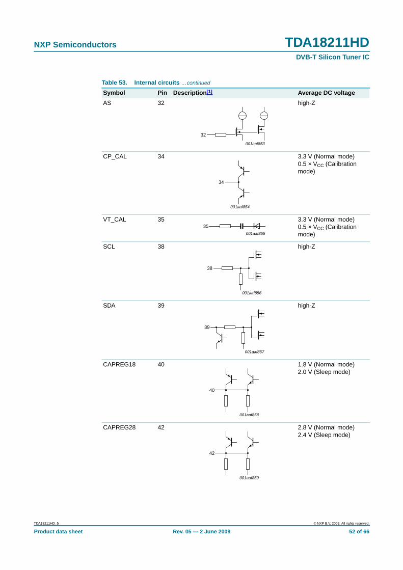
NXP Semiconductors TDA18211HDDVB-T Silicon Tuner IC
AS 32 high-Z
CP_CAL 34 3.3 V (Normal mode)0.5 × VCC (Calibrationmode)
VT_CAL 35 3.3 V (Normal mode)0.5 × VCC (Calibrationmode)
SCL 38 high-Z
SDA 39 high-Z
CAPREG18 40 1.8 V (Normal mode)2.0 V (Sleep mode)
CAPREG28 42 2.8 V (Normal mode)2.4 V (Sleep mode)
Table 53. Internal circuits …continued
Symbol Pin Description [1] Average DC voltage
001aaf853
32
001aaf854
34
001aaf855
35
001aaf856
38
001aaf857
39
001aaf858
40
001aaf859
42
TDA18211HD_5 © NXP B.V. 2009. All rights reserved.
Product data sheet Rev. 05 — 2 June 2009 52 of 66

NXP Semiconductors TDA18211HDDVB-T Silicon Tuner IC
[1] ESD protection components are not shown.
11. Limiting values
[1] The TDA18211HD withstands the latch-up specifications of JEDEC (JESD78A), with the specificrecommendation using coupling capacitors on pins RF_IN, LT, STO, XTOUTP and XTOUTN.
IFOUTN 45 1.35 V
IFOUTP 46 1.35 V
V_IFAGC 47 high-Z
VSYNC 51 high-Z
CAPREGFILTRF 52 2.8 V (Normal mode)0 V (Sleep mode)
Table 53. Internal circuits …continued
Symbol Pin Description [1] Average DC voltage
001aaf860
45
001aaf861
46
001aaf862
47
001aaf863
51
001aaf864
52
Table 54. Limiting values [1]
In accordance with the Absolute Maximum Rating System (IEC 60134).
Symbol Parameter Conditions Min Max Unit
VCC supply voltage −0.3 +3.6 V
VI input voltage pins SDA and SCL −0.3 +5.5 V
all other pins
VCC < 3.3 V −0.3 VCC + 0.3 V
VCC > 3.3 V −0.3 +3.6 V
Tstg storage temperature −40 +150 °C
Tj junction temperature - 110 °C
Vesd electrostaticdischarge voltage
EIA/JESD22-A114 (humanbody model)
±2000 - V
EIA/JESD22-A115 (machinemodel)
±200 - V
TDA18211HD_5 © NXP B.V. 2009. All rights reserved.
Product data sheet Rev. 05 — 2 June 2009 53 of 66

NXP Semiconductors TDA18211HDDVB-T Silicon Tuner IC
12. Thermal characteristics
[1] The junction temperature can be obtained with the formula Tj = Tamb + Rth(j-a) × VCC × ICC, where Rth(j-a) isthe thermal resistance of the application. Rth(j-a) must be such that the resulting Tj does not exceed themaximum value defined in Table 54.
13. Characteristics
All data in this section refers to Master mode operation.
[1] Channel loading assumptions: 129 channels (NTSC 129 frequency plan) at 75 dBµV.
Table 55. Thermal characteristics [1]
Symbol Parameter Conditions Typ Unit
Rth(j-c) thermal resistancefrom junction to case
according to JEDECspecification
19.6 K/W
Table 56. Loop-through characteristics (RF input to loop-through output)Tamb = 25 °C; VCC = 3.3 V; for test circuit see Figure 26; unless otherwise specified.
Symbol Parameter Conditions Min Typ Max Unit
fRF(lt) loop-through RFfrequency
center of channel 45 - 864 MHz
VSWR voltage standingwave ratio
loop-through output; 75 Ωnominal impedance
- - 3 -
Gv(lt) loop-through voltagegain
75 Ω load - 1.5 - dB
∆Glt loop-through gainvariation
in the RF frequency range;75 Ω load
- 3 - dB
NFlt loop-through noisefigure
Normal mode - 5.5 - dB
CSO compositesecond-orderdistortion
[1] - −60 - dBc
CTB composite triple beat [1] - −63 - dBc
αisol(bp) bypass isolation from loop-through output toRF input
- 24 - dB
VL(tun-lto) leakage voltagebetween tuner andloop-through output
in RF TV band - 10 - dBµV
TDA18211HD_5 © NXP B.V. 2009. All rights reserved.
Product data sheet Rev. 05 — 2 June 2009 54 of 66

NXP Semiconductors TDA18211HDDVB-T Silicon Tuner IC
Table 57. Slave tuner output characteristics (pin STO)Tamb = 25 °C; VCC = 3.3 V; for test circuit see Figure 26; unless otherwise specified.
Symbol Parameter Conditions Min Typ Max Unit
fRF(STO) RF frequency on pinSTO
45 - 864 MHz
Zo(STO) output impedance onpin STO
30 35 40 Ω
Gv(STO) voltage gain on pinSTO
75 Ω source resistance onRF input; Zi = 35 Ω (75 Ω,VSWR = 2)
POWER_LEVEL[6:5] = 00 - 6 - dB
POWER_LEVEL[6:5] = 01 - 9 - dB
POWER_LEVEL[6:5] = 10 - 12 - dB
POWER_LEVEL[6:5] = 11 - 15 - dB
Table 58. General characteristics for TV reception (RF input to IF output)Tamb = 25 °C; VCC = 3.3 V; IF output level option = 2 V (p-p); IF output load = 1 kΩ on each terminal;for test circuit see Figure 26; unless otherwise specified.
Symbol Parameter Conditions Min Typ Max Unit
Supply
VCC supply voltage 3.13 3.30 3.47 V
ICC supply current Normal mode 180 235 290 mA
Standby mode withloop-through and crystaloscillator on (default at POR)
40 51 65 mA
Standby mode with onlycrystal oscillator on
10 15 20 mA
Device off mode 1 2 5 mA
P power dissipation - 780 - mW
Tamb ambienttemperature
0 - 70 °C
Input
fRF RF frequency center of channel 174 - 864 MHz
VSWR voltage standingwave ratio
RF input; 75 Ω nominalimpedance
- 2 3 -
NFtun tuner noise figure maximum gain - 5.5 6 dB
Gv(tun)max maximum tunervoltage gain
2 V (p-p) IF output selection 71 83 90 dB
∆GAGC(tun) tuner AGC gainrange
68 71 80 dB
Vi(max) maximum inputvoltage
1 dB gain compression, oneanalog TV signal at RF input(−5 dBm)
- 103 - dBµV
VL(tun-RF) leakage voltagebetween tuner andRF
at RF input; in RF band - 0 - dBµV
TDA18211HD_5 © NXP B.V. 2009. All rights reserved.
Product data sheet Rev. 05 — 2 June 2009 55 of 66

NXP Semiconductors TDA18211HDDVB-T Silicon Tuner IC
[1] Measured with TDA10048HN channel decoder.
Output
Vo(IF)dif(p-p) peak-to-peakdifferential IF outputvoltage
IF_LEVEL[2:0] = 000 - 2 - V
IF_LEVEL[2:0] = 001 - 1.25 - V
IF_LEVEL[2:0] = 010 - 1 - V
IF_LEVEL[2:0] = 111 - 0.5 - V
Zo(IF) IF outputimpedance
differential mode; magnitudevalue
- 100 - Ω
∆GAGC(IF) IF AGC GAIN range 2 V (p-p) IF output voltageselection
- 30 - dB
Gtlt tilt gain RF frequency range;6/7/8 MHz channel
- 2 4 dB
fIF(stpb)lp low-pass stop-bandIF frequency
60 dB attenuation
6 MHz IF filter - 14 - MHz
7 MHz IF filter - 16 - MHz
8 MHz IF filter - 18 - MHz
αimage image rejection 53 65 - dB
tripple ripple time digital TV; difference betweenf1 and f2 in digital channel
ATSC 6 MHz;f1 = 0.75 MHz;f2 = 5.75 MHz
- 395 - ns
DVB-T 6 MHz; f1 = 0.8 MHzand f2 = 5.8 MHz
- 365 - ns
DVB-T 7 MHz; f1 = 0.5 MHzand f2 = 6.5 MHz
- 478 - ns
DVB-T 8 MHz; f1 = 0.5 MHzand f2 = 7.5 MHz
- 515 - ns
QAM 6 MHz; f1 = 1.5 MHzand f2 = 6.5 MHz
- 155 - ns
QAM 8 MHz; f1 = 1.5 MHzand f2 = 8.5 MHz
- 180 - ns
ϕn phase noise 1 kHz and 10 kHz, details seeFigure 23
- −89 - dBc/Hz
αIF IF rejection 9 MHz Low-pass filter
13.75 MHz
18 MHz
35
56
42
66
-
dB
dB
Various
tstartup(tun) tuner start-up time at power-up - 1.5 - s
tset setting time PLL setting time; channelchange
- - 5 ms
Sdig digital sensitivity DVB-T (64 QAM 2⁄3);BER = 2.10−4
[1] - −82 - dBm
Table 58. General characteristics for TV reception (RF input to IF output) …continuedTamb = 25 °C; VCC = 3.3 V; IF output level option = 2 V (p-p); IF output load = 1 kΩ on each terminal;for test circuit see Figure 26; unless otherwise specified.
Symbol Parameter Conditions Min Typ Max Unit
TDA18211HD_5 © NXP B.V. 2009. All rights reserved.
Product data sheet Rev. 05 — 2 June 2009 56 of 66

NXP Semiconductors TDA18211HDDVB-T Silicon Tuner IC
[1] Devices that use non-standard supply voltages, which do not conform the intended I2C-bus system levels,must relate their input levels to the supply voltage to which the pull-up resistors are connected.
Table 59. Characteristics of terminalsTamb = 25 °C; VCC = 3.3 V; 2.2 nF on input pin V_IFAGC; for test circuit see Figure 26; unlessotherwise specified.
Symbol Parameter Conditions Min Typ Max Unit
IF AGC input: pin V_IFAGC
VAGC AGC voltage 0 - VCC V
Zi input impedance - high-Z - Ω
dGAGC/dV rate of change ofAGC gain withvoltage
- 30 55 dB/V
Crystal oscillator
fxtal crystal frequency 15.99 16 16.01 MHz
Zi input impedance magnitude value - 500 - Ω
Crystal oscillator output buffer; pins XTOUTP and XTOUTN
Ro output resistance 16 MHz output frequency - 460 - Ω
Vo(p-p) peak-to-peakoutput voltage
10 kΩ//10 pF AC load - 0.4 - V
SRr slew rate of risingsignal
10 kΩ//10 pF AC load - 40 - V/µs
SRf slew rate of fallingsignal
10 kΩ//10 pF AC load - 40 - V/µs
I2C-bus [1]
Pin SCL
VIL LOW-level inputvoltage
fixed input levels - - 1.5 V
VDD related input levels - - 0.3VDD V
VIH HIGH-level inputvoltage
fixed input levels 3 - - V
VDD related input levels 0.7VDD - - V
fSCL SCL clockfrequency
- - 400 kHz
Pin SDA
VOH HIGH-level outputvoltage
ISDA = 3 mA (sink current) - - 0.4 V
VIL LOW-level inputvoltage
fixed input levels - - 1.5 V
VDD related input levels - - 0.3VDD V
VIH HIGH-level inputvoltage
fixed input levels 3 - - V
VDD related input levels 0.7VDD - - V
TDA18211HD_5 © NXP B.V. 2009. All rights reserved.
Product data sheet Rev. 05 — 2 June 2009 57 of 66
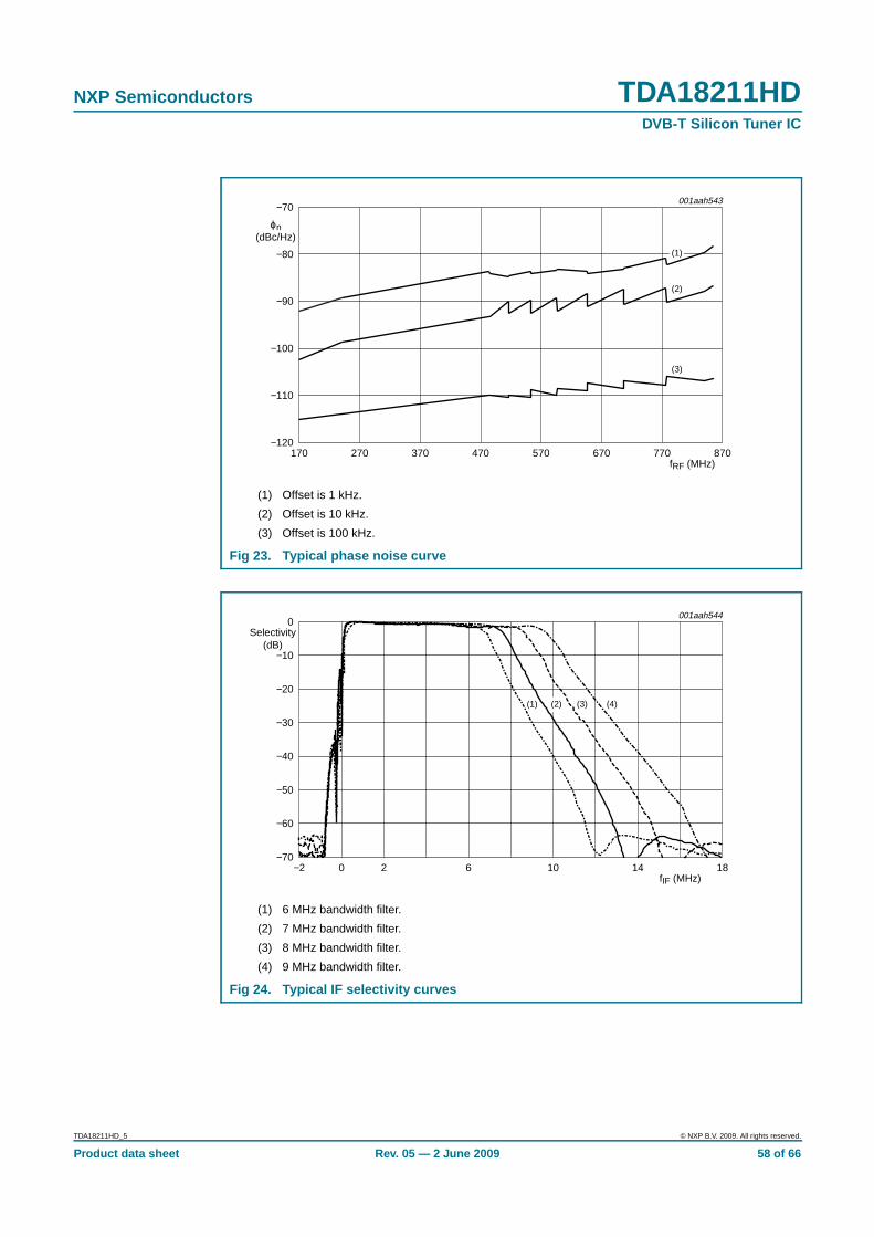
NXP Semiconductors TDA18211HDDVB-T Silicon Tuner IC
(1) Offset is 1 kHz.
(2) Offset is 10 kHz.
(3) Offset is 100 kHz.
Fig 23. Typical phase noise curve
(1) 6 MHz bandwidth filter.
(2) 7 MHz bandwidth filter.
(3) 8 MHz bandwidth filter.
(4) 9 MHz bandwidth filter.
Fig 24. Typical IF selectivity curves
fRF (MHz)170 870670 770470 570370270
001aah543
−100
−90
−110
−80
−70
ϕn(dBc/Hz)
−120
(2)
(3)
(1)
001aah544
fIF (MHz)−2 18146 102
−30
−50
−10
0Selectivity
(dB)
−70
−20
−40
−60
0
(1) (2) (3) (4)
TDA18211HD_5 © NXP B.V. 2009. All rights reserved.
Product data sheet Rev. 05 — 2 June 2009 58 of 66

NXP Semiconductors TDA18211HDDVB-T Silicon Tuner IC
14. Application information
14.1 Application example
14.2 Application notesPlease contact the NXP sales office for additional information on dual-tuner DVB-Tapplications.
Fig 25. Example for TDA18211HD of DVB-T dual-tuner reception
001aah541
XTAL
SURGEPROTECTION
STO
LTO
RF_INRF
RF
SILICON TUNERTDA18211
MASTER MODE
V_IFAGC
I2C-bus (gated)
V_IFAGC
I2C-bus (gated)
IFOUTP
IFOUTN
IFOUTP
IFOUTN
3.3 V3.3 V1.2 V
I2C-bus
3.3 V3.3 V1.2 V
I2C-bus
XTO
UT
P
XTOUTPXTOUTN
reference frequency
XTO
UT
N
MA
ST
ER
SY
NC
FR
EE
ZE
CHANNELRECEIVERTDA10048
TSSURGE
PROTECTIONTV
SILICON TUNERTDA18211
SLAVE MODE
CHANNELRECEIVERTDA10048
TS
TDA18211HD_5 © NXP B.V. 2009. All rights reserved.
Product data sheet Rev. 05 — 2 June 2009 59 of 66

xxxx xxxxxxxxxxxxxxxxxxxxxxxxxxxxxx x xxxxxxxxxxxxxx xxxxxxxxxx xxx xxxxxx xxxxxxxxxxxxxxxxxxxxxxx xxxxxxxxxxxxxxxxxxxxxxxxxxx xxxxxx xx xxxxxxxxxxxxxxxxxxxxxxxxxxxxx xxxxxxxxxxxxxxxxxxxxxx xxxxxxxxxxx xxxxxxx xxxxxxxxxxxxxxxxxxxxxxxxxxxxxxxxxxx xxxxxxxxxxxxxx xxxxxx xx xxxxxxxxxxxxxxxxxxxxxxxxxxxxxxxx xxxxxxxxxxxxxxxxxxxxxxxx xxxxxxxxxxxxxxxxxxxxxxxxxxxxxxxxxxxxxxxxxxxxxxxxxxxxx xxxxxxxxxxx xxxxx x x
TD
A18211H
D_5
Product data shee
NX
P S
emiconducto
15.Test inform
at
R118
R117150 kΩ
56 Ω
V_IFAGC_MTP104VSYNC_M
J109
IFoutP_MJ108
C127100 nF
R115
C1262.2 nF
SDAVCC3.3
2
3
4
5
6
GND
SDA
VCC3.3
t
R116
470 Ω
RE
GF
ILT
RF
NC
C125
100 nF
ST1SCL
J1R12.2kΩ
R22.2kΩ
1SCL
rsT
DA
18211HD
DV
B-T
Silicon Tuner IC
ion
001aah542
UTN_M
VCC2
C12347 nF
C120220 nF
C1193.9 nFF
UTP_M
M
56 Ω
R113
120 Ω
2
Ω
IFoutN_MJ107
EEZE
_CMOT
© N
XP
B.V. 2009. A
ll rights reserved.
Rev. 05 —
2 June 200960 of 66 Fig 26. Test circuit
R107 R108
Y1
470 Ω 390 Ω
CP
_LO
C1126.8 nF
16 MHz
C11333 pF
Cxx
5.6 pF C20033 pF
C1111 nF
C110220 nF
TDA18211HD
GND 64 6263 6061 5859 5657 5455 5253
XO
50 4948
51
1817 2019 2221 2423 2625 2827 3029 3231
GN
D
GN
D
GN
D
GN
D
GN
D
GN
D
GN
D
GN
D
GN
D
GN
D
GN
D
GN
D
CA
P
VS
Y
GN
D
GN
D
GND
GND
GND
GND
GND
GND
GND
47V_IFAGC
46 IFOUTP
45 IFOUTN
44
43
42
41
40
39
38
37
36
35
34
33
1
2
3
4
5
6
7
8
9
10
11
12
13
14
15
16
VCC
GNDCAPREG28
GND
CAPREG18
SDA
SCLSDA
SCLGND
GNDVT_CAL
CP_CAL
VCC
n.c.
VCCRF_IN
RFIN_M
GND
CAPRFAGC
LTGND
C12847 nF
C102
1 nF_5 %
1 nF_5 %
1 nF_5 %
VCC1
LT_M
VCC2
VCC3
VCC2
C103
220 nF
J102
C10547 nF
C11747 nF
C1186.8 n
C122
100 nF
C121
C115
4.7 nF
XO
XOUTP_TP103
C114
4.7 nF
R114
470 Ω
R11
390
C124
100 nF
C10847 nF
C107100 nF
C109100 nF
STOSP_M
VCC
VC
C
MA
ST
ER
SY
NC
CA
PF
ILT
VC
OV
T_C
OA
RS
E
VT
_FIN
E
GN
D
GN
D
XT
ALP
XT
ALN
R10539 Ω
CA
PR
EG
VC
O
FR
EE
ZE
XT
OU
T_M
S
XT
OU
TP
XT
OU
TN
AS
C104J103
SP_M SP_M
RFIN_S
R104
n.c.
C106J104
MASTERSYNC
MASTERSYNC
J105
10 nF
CAPRFAGCTP101
FR
FREEZETP102
VCC3.3

NXP Semiconductors TDA18211HDDVB-T Silicon Tuner IC
16. Package outline
Fig 27. Package outline SOT903-1 (HLQFN64R)
REFERENCESOUTLINEVERSION
EUROPEANPROJECTION
ISSUE DATEIEC JEDEC JEITA
SOT903-1
SOT903-1
06-03-2907-11-14
UNIT Amax
mm 1.7 0.30.2
9.18.9
9.18.9
2.922.82
0.310.21
0.450.40
0.180.08
b
DIMENSIONS (mm are the original dimensions)
HLQFN64R; plastic thermal enhanced low profile quad flat package; no leads;64 terminals; resin based; body 9 × 9 × 1.6 mm
D Dh
0.860.76
Dj
3.323.22
Dk
1.791.69
Dl
2.162.06
Dm E Eh
0.690.59
Ej
1.791.69
Ek
0.790.69
El
2.632.53
Em
2.021.92
En e e1 e2
7.57.50.5
L
L1 v
0.1
w y
0.050.05
y1
0.1
0 2.5 5 mm
scale
- - -- - -- - -
B Aterminal 1index area
D
E
C
yCy1
X
A
detail X
b
terminal 1index area
e1
e 1/2 e
e2
e
1/2 e
AC Bv M
Cw ML1L
EhEjEl
Ek
Em
En
Dh
Dj
Dk Dl
Dm
1
17
16
32
33
48
4964
TDA18211HD_5 © NXP B.V. 2009. All rights reserved.
Product data sheet Rev. 05 — 2 June 2009 61 of 66

NXP Semiconductors TDA18211HDDVB-T Silicon Tuner IC
17. Printed-circuit board
17.1 Reflow profileSee application note AN10366.
17.2 Desoldering recommendationSee application notes AN10366.
TDA18211HD_5 © NXP B.V. 2009. All rights reserved.
Product data sheet Rev. 05 — 2 June 2009 62 of 66

NXP Semiconductors TDA18211HDDVB-T Silicon Tuner IC
17.3 Footprint layout
Fig 28. Footprint HLQFN64R (SOT903-1)
DIMENSIONS in mm
Ax Ay Bx By D Hx SLx SLx1 SLy SLy1 SPx SPx1 SPx2 SPy
9.000 9.000 7.880 7.880
P
0.500 0.250
C
0.555 9.500
Hy
9.500 4.610 1.740 3.220 0.640 0.800 2.065 0.3 0.7
SPy1
0.3
Vy2 Vy3
0.8 0.9
Vx Vy1
0.8 0.9
Vd Vd1
0.35 0.5
D P 1/2 P
Bx
Hx
Hy
Ax
By Ay
0.065
SLy1
SLy
0.12
SPy
Vy2
Vy1
SPy1
Vd1
Vx
SPx2
SPx1 SLx1
SLx
C
solder resist
occupied area
solder lands
solder paste
Vd
Vy3
SPx
TDA18211HD_5 © NXP B.V. 2009. All rights reserved.
Product data sheet Rev. 05 — 2 June 2009 63 of 66

NXP Semiconductors TDA18211HDDVB-T Silicon Tuner IC
18. Abbreviations
19. Revision history
Table 60. Abbreviations
Acronym Description
AGC Automatic Gain Control
DVB-T Digital Video Broadcasting - Terrestrial
DVR Digital Video Recorder
ESD ElectroStatic Discharge
IF Intermediate Frequency
LNA Low Noise Amplifier
LO Local Oscillator
PLL Phase-Lock Loop
QAM Quadrature Amplitude Modulation
RoHS Restriction of Hazardous Substances
SAW Surface Acoustic Wave
STB Set-Top Box
VCO Voltage-Controlled Oscillator
Table 61. Revision history
Document ID Release date Data sheet status Change notice Supersedes
TDA18211HD_5 20090602 Product data sheet - TDA18211HD_4
Modifications: • Figure 21 “Flowchart TDA18211Read” updated
TDA18211HD_4 20090505 Product data sheet - TDA18211HD_3
TDA18211HD_3 20080304 Product data sheet - TDA18211HD_2
TDA18211HD_2 20071121 Product data sheet - TDA18211HD_1
TDA18211HD_1 20070802 Product data sheet - -
TDA18211HD_5 © NXP B.V. 2009. All rights reserved.
Product data sheet Rev. 05 — 2 June 2009 64 of 66

NXP Semiconductors TDA18211HDDVB-T Silicon Tuner IC
20. Legal information
20.1 Data sheet status
[1] Please consult the most recently issued document before initiating or completing a design.
[2] The term ‘short data sheet’ is explained in section “Definitions”.
[3] The product status of device(s) described in this document may have changed since this document was published and may differ in case of multiple devices. The latest product statusinformation is available on the Internet at URL http://www.nxp.com.
20.2 Definitions
Draft — The document is a draft version only. The content is still underinternal review and subject to formal approval, which may result inmodifications or additions. NXP Semiconductors does not give anyrepresentations or warranties as to the accuracy or completeness ofinformation included herein and shall have no liability for the consequences ofuse of such information.
Short data sheet — A short data sheet is an extract from a full data sheetwith the same product type number(s) and title. A short data sheet is intendedfor quick reference only and should not be relied upon to contain detailed andfull information. For detailed and full information see the relevant full datasheet, which is available on request via the local NXP Semiconductors salesoffice. In case of any inconsistency or conflict with the short data sheet, thefull data sheet shall prevail.
20.3 Disclaimers
General — Information in this document is believed to be accurate andreliable. However, NXP Semiconductors does not give any representations orwarranties, expressed or implied, as to the accuracy or completeness of suchinformation and shall have no liability for the consequences of use of suchinformation.
Right to make changes — NXP Semiconductors reserves the right to makechanges to information published in this document, including withoutlimitation specifications and product descriptions, at any time and withoutnotice. This document supersedes and replaces all information supplied priorto the publication hereof.
Suitability for use — NXP Semiconductors products are not designed,authorized or warranted to be suitable for use in medical, military, aircraft,space or life support equipment, nor in applications where failure ormalfunction of an NXP Semiconductors product can reasonably be expectedto result in personal injury, death or severe property or environmentaldamage. NXP Semiconductors accepts no liability for inclusion and/or use ofNXP Semiconductors products in such equipment or applications andtherefore such inclusion and/or use is at the customer’s own risk.
Applications — Applications that are described herein for any of theseproducts are for illustrative purposes only. NXP Semiconductors makes norepresentation or warranty that such applications will be suitable for thespecified use without further testing or modification.
Limiting values — Stress above one or more limiting values (as defined inthe Absolute Maximum Ratings System of IEC 60134) may cause permanentdamage to the device. Limiting values are stress ratings only and operation ofthe device at these or any other conditions above those given in theCharacteristics sections of this document is not implied. Exposure to limitingvalues for extended periods may affect device reliability.
Terms and conditions of sale — NXP Semiconductors products are soldsubject to the general terms and conditions of commercial sale, as publishedat http://www.nxp.com/profile/terms, including those pertaining to warranty,intellectual property rights infringement and limitation of liability, unlessexplicitly otherwise agreed to in writing by NXP Semiconductors. In case ofany inconsistency or conflict between information in this document and suchterms and conditions, the latter will prevail.
No offer to sell or license — Nothing in this document may be interpretedor construed as an offer to sell products that is open for acceptance or thegrant, conveyance or implication of any license under any copyrights, patentsor other industrial or intellectual property rights.
Export control — This document as well as the item(s) described hereinmay be subject to export control regulations. Export might require a priorauthorization from national authorities.
Quick reference data — The Quick reference data is an extract of theproduct data given in the Limiting values and Characteristics sections of thisdocument, and as such is not complete, exhaustive or legally binding.
20.4 Licenses
20.5 TrademarksNotice: All referenced brands, product names, service names and trademarksare the property of their respective owners.
I2C-bus — logo is a trademark of NXP B.V.
Silicon Tuner — is a trademark of NXP B.V.
21. Contact information
For more information, please visit: http://www .nxp.com
For sales office addresses, please send an email to: salesad [email protected]
Document status [1] [2] Product status [3] Definition
Objective [short] data sheet Development This document contains data from the objective specification for product development.
Preliminary [short] data sheet Qualification This document contains data from the preliminary specification.
Product [short] data sheet Production This document contains the product specification.
ICs with DVB-T functionality
Use of this product in any manner that complies with the DVB-T Standardmay require licenses under applicable patents in the DVB-T patent portfolio,which license is available from Sisvel S.p.A., Via Sestriere 100, 10060 None(TO), Italy, and under applicable patents of other parties.
TDA18211HD_5 © NXP B.V. 2009. All rights reserved.
Product data sheet Rev. 05 — 2 June 2009 65 of 66

NXP Semiconductors TDA18211HDDVB-T Silicon Tuner IC
22. Contents
1 General description . . . . . . . . . . . . . . . . . . . . . . 12 Features . . . . . . . . . . . . . . . . . . . . . . . . . . . . . . . 13 Applications . . . . . . . . . . . . . . . . . . . . . . . . . . . . 13.1 Target applications . . . . . . . . . . . . . . . . . . . . . . 13.2 Key benefits . . . . . . . . . . . . . . . . . . . . . . . . . . . 24 Quick reference data . . . . . . . . . . . . . . . . . . . . . 25 Ordering information . . . . . . . . . . . . . . . . . . . . . 26 Block diagram . . . . . . . . . . . . . . . . . . . . . . . . . . 37 Pinning information . . . . . . . . . . . . . . . . . . . . . . 47.1 Pinning . . . . . . . . . . . . . . . . . . . . . . . . . . . . . . . 47.2 Pin description . . . . . . . . . . . . . . . . . . . . . . . . . 48 Functional description . . . . . . . . . . . . . . . . . . . 68.1 Master and slave operation. . . . . . . . . . . . . . . . 68.2 Tuner outputs . . . . . . . . . . . . . . . . . . . . . . . . . . 68.2.1 Loop-through output . . . . . . . . . . . . . . . . . . . . . 68.2.2 Slave tuner output. . . . . . . . . . . . . . . . . . . . . . . 68.3 Crystal input mode . . . . . . . . . . . . . . . . . . . . . . 78.4 Crystal output mode . . . . . . . . . . . . . . . . . . . . . 79 Control interface . . . . . . . . . . . . . . . . . . . . . . . . 79.1 I2C-bus format, write/read mode. . . . . . . . . . . . 79.2 I2C-bus at power-on reset. . . . . . . . . . . . . . . . 109.3 Description of symbols used in I2C-bus
format table. . . . . . . . . . . . . . . . . . . . . . . . . . . 119.3.1 I2C-bus address selection. . . . . . . . . . . . . . . . 139.3.2 Description of chip ID byte . . . . . . . . . . . . . . . 139.3.3 Description of temperature sensor byte . . . . . 139.3.4 Description of power level byte (read mode) . 149.3.5 Description of Easy Prog byte 1 . . . . . . . . . . . 159.3.6 Description of Easy Prog byte 2 . . . . . . . . . . . 159.3.7 Description of Easy Prog byte 3 . . . . . . . . . . . 159.3.8 Description of Easy Prog byte 4 . . . . . . . . . . . 169.3.9 Description of Easy Prog byte 5 . . . . . . . . . . . 179.3.10 Description of Cal Post-Divider byte . . . . . . . . 179.3.11 Description of Cal divider bytes 1, 2 and 3 . . . 179.3.12 Description of Main Post-Divider byte. . . . . . . 189.3.13 Description of Main divider bytes 1, 2 and 3. . 189.3.14 Description of Extended bytes 1 to 23 . . . . . . 199.4 I2C-bus programming flowcharts . . . . . . . . . . 229.4.1 Flowchart explanation. . . . . . . . . . . . . . . . . . . 229.4.2 Flowchart TDA18211SetRf_dual . . . . . . . . . . 259.4.3 Flowchart TDA18211InitCal . . . . . . . . . . . . . . 269.4.4 Flowchart TDA18211FixedContentsI2Cupdate 279.4.5 Flowchart TDA18211CalcRFFilterCurve . . . . 289.4.6 Flowchart TDA18211RFTrackingFiltersInit . . . 299.4.7 Flowchart TDA18211PowerScanInit . . . . . . . . 319.4.8 Flowchart TDA18211PowerScan . . . . . . . . . . 31
9.4.9 Flowchart TDA18211CalibrateRF . . . . . . . . . 339.4.10 Flowchart TDA18211MSPOR . . . . . . . . . . . . 359.4.11 Flowchart
TDA18211RFtrackingFiltersCorrection . . . . . 359.4.12 Flowchart TDA18211ChannelConfiguration. . 379.4.13 Flowchart TDA18211CalcMAINPLL. . . . . . . . 399.4.14 Flowchart TDA18211CalcCALPLL. . . . . . . . . 409.4.15 Flowchart TDA18211ThermometerRead . . . . 419.4.16 Flowchart TDA18211Read. . . . . . . . . . . . . . . 429.4.17 Flowchart TDA18211ReadExtended . . . . . . . 439.5 Maps . . . . . . . . . . . . . . . . . . . . . . . . . . . . . . . 4310 Internal circuitry . . . . . . . . . . . . . . . . . . . . . . . 4911 Limiting values . . . . . . . . . . . . . . . . . . . . . . . . 5312 Thermal characteristics . . . . . . . . . . . . . . . . . 5413 Characteristics . . . . . . . . . . . . . . . . . . . . . . . . 5414 Application information . . . . . . . . . . . . . . . . . 5914.1 Application example . . . . . . . . . . . . . . . . . . . . 5914.2 Application notes . . . . . . . . . . . . . . . . . . . . . . 5915 Test information. . . . . . . . . . . . . . . . . . . . . . . . 6016 Package outline . . . . . . . . . . . . . . . . . . . . . . . . 6117 Printed-circuit board . . . . . . . . . . . . . . . . . . . . 6217.1 Reflow profile . . . . . . . . . . . . . . . . . . . . . . . . . 6217.2 Desoldering recommendation . . . . . . . . . . . . 6217.3 Footprint layout. . . . . . . . . . . . . . . . . . . . . . . . 6318 Abbreviations . . . . . . . . . . . . . . . . . . . . . . . . . 6419 Revision history . . . . . . . . . . . . . . . . . . . . . . . 6420 Legal information . . . . . . . . . . . . . . . . . . . . . . 6520.1 Data sheet status . . . . . . . . . . . . . . . . . . . . . . 6520.2 Definitions . . . . . . . . . . . . . . . . . . . . . . . . . . . 6520.3 Disclaimers. . . . . . . . . . . . . . . . . . . . . . . . . . . 6520.4 Licenses . . . . . . . . . . . . . . . . . . . . . . . . . . . . . 6520.5 Trademarks . . . . . . . . . . . . . . . . . . . . . . . . . . 6521 Contact information . . . . . . . . . . . . . . . . . . . . 6522 Contents. . . . . . . . . . . . . . . . . . . . . . . . . . . . . . 66
© NXP B.V. 2009. All rights reserved.For more information, please visit: http://www.nxp.comFor sales office addresses, please send an email to: [email protected]
Date of release: 2 June 2009
Document identifier: TDA18211HD_5
Please be aware that important notices concerning this document and the product(s)described herein, have been included in section ‘Legal information’.