tc1165 tc1166 ds - digi-key sheets/infineon pdfs/tc1165_66.pdf · 112 4.3.6 debug trace ... figure...
TRANSCRIPT

Data Sheet, V0.2, Feb. 2006
Microcontrol lers
TC1165/TC116632-Bit Single-Chip Microcontrol lerTr iCoreTM

Edition 2006-02Published by Infineon Technologies AG, 81726 München, Germany© Infineon Technologies AG 2006. All Rights Reserved.
Attention please!The information herein is given to describe certain components and shall not be considered as a guarantee of characteristics.Terms of delivery and rights to technical change reserved.We hereby disclaim any and all warranties, including but not limited to warranties of non-infringement, regarding circuits, descriptions and charts stated herein.
InformationFor further information on technology, delivery terms and conditions and prices please contact your nearest Infineon Technologies Office (www.infineon.com).
WarningsDue to technical requirements components may contain dangerous substances. For information on the types in question please contact your nearest Infineon Technologies Office.Infineon Technologies Components may only be used in life-support devices or systems with the express written approval of Infineon Technologies, if a failure of such components can reasonably be expected to cause the failure of that life-support device or system, or to affect the safety or effectiveness of that device or system. Life support devices or systems are intended to be implanted in the human body, or to support and/or maintain and sustain and/or protect human life. If they fail, it is reasonable to assume that the health of the user or other persons may be endangered.

Data Sheet, V0.2, Feb. 2006
Microcontrol lers
TC1165/TC116632-Bit Single-Chip Microcontrol lerTr iCoreTM

Template: mc_a5_um_tmplt.fm / 5 / 2005-10-01
TC1165/TC1166
Revision History: 2006-02 V0.2Previous Version: V0.1, December 2005Page Subjects (major changes since last revision)3-82 The reset value for RTID is corrected.4-95 A new footnote is added to VAREF.4-100 The footnote on FADC callibration interval is updated.4-105 Max. values for power supply current section is defined.4-116 A new section is added for JTAG signals timing based on 40 MHz JTAG
clock.
We Listen to Your CommentsAny information within this document that you feel is wrong, unclear or missing at all? Your feedback will help us to continuously improve the quality of this document. Please send your proposal (including a reference to this document) to:[email protected]

TC1165/TC1166
Table of ContentsAdvance Information
Table of Contents
1 Summary of Features . . . . . . . . . . . . . . . . . . . . . . . . . . . . . . . . . . . . . . . . 32 General Device Information . . . . . . . . . . . . . . . . . . . . . . . . . . . . . . . . . . . 62.1 Block Diagram . . . . . . . . . . . . . . . . . . . . . . . . . . . . . . . . . . . . . . . . . . . . . . . 62.2 Logic Symbol . . . . . . . . . . . . . . . . . . . . . . . . . . . . . . . . . . . . . . . . . . . . . . . . 72.3 Pin Configuration . . . . . . . . . . . . . . . . . . . . . . . . . . . . . . . . . . . . . . . . . . . . . 82.4 Pad Driver and Input Classes Overview . . . . . . . . . . . . . . . . . . . . . . . . . . . 92.5 Pin Definitions and Functions . . . . . . . . . . . . . . . . . . . . . . . . . . . . . . . . . . 10
3 Functional Description . . . . . . . . . . . . . . . . . . . . . . . . . . . . . . . . . . . . . . 243.1 System Architecture and On-Chip Bus Systems . . . . . . . . . . . . . . . . . . . . 243.2 On-Chip Memories . . . . . . . . . . . . . . . . . . . . . . . . . . . . . . . . . . . . . . . . . . . 253.3 Memory Maps . . . . . . . . . . . . . . . . . . . . . . . . . . . . . . . . . . . . . . . . . . . . . . 273.3.1 Architectural Address Map . . . . . . . . . . . . . . . . . . . . . . . . . . . . . . . . . . . 273.3.2 How to Read the Address Maps . . . . . . . . . . . . . . . . . . . . . . . . . . . . . . 293.3.3 Contents of the Segments . . . . . . . . . . . . . . . . . . . . . . . . . . . . . . . . . . . 303.3.4 Address Map of the FPI Bus System . . . . . . . . . . . . . . . . . . . . . . . . . . . 323.3.4.1 Segments 0 to 14 . . . . . . . . . . . . . . . . . . . . . . . . . . . . . . . . . . . . . . . . 323.3.4.2 Segment 15 . . . . . . . . . . . . . . . . . . . . . . . . . . . . . . . . . . . . . . . . . . . . 353.3.5 Address Map of the Local Memory Bus (LMB) . . . . . . . . . . . . . . . . . . . 403.4 Memory Protection System . . . . . . . . . . . . . . . . . . . . . . . . . . . . . . . . . . . . 443.5 Peripheral Control Processor . . . . . . . . . . . . . . . . . . . . . . . . . . . . . . . . . . . 443.6 DMA Controller and Memory Checker . . . . . . . . . . . . . . . . . . . . . . . . . . . . 473.7 Interrupt System . . . . . . . . . . . . . . . . . . . . . . . . . . . . . . . . . . . . . . . . . . . . 493.8 Asynchronous/Synchronous Serial Interfaces (ASC0, ASC1) . . . . . . . . . . 513.9 High-Speed Synchronous Serial Interfaces (SSC0 and SSC1) . . . . . . . . . 533.10 Micro Second Bus Interface (MSC0) . . . . . . . . . . . . . . . . . . . . . . . . . . . . . 553.11 MultiCAN Controller (CAN) . . . . . . . . . . . . . . . . . . . . . . . . . . . . . . . . . . . . 573.12 Micro Link Serial Bus Interface (MLI0, MLI1) . . . . . . . . . . . . . . . . . . . . . . . 593.13 General Purpose Timer Array . . . . . . . . . . . . . . . . . . . . . . . . . . . . . . . . . . 613.13.1 Functionality of GPTA0 . . . . . . . . . . . . . . . . . . . . . . . . . . . . . . . . . . . . . 623.14 Analog-to-Digital Converter (ADC0) . . . . . . . . . . . . . . . . . . . . . . . . . . . . . 653.15 Fast Analog-to-Digital Converter Unit (FADC) . . . . . . . . . . . . . . . . . . . . . . 673.16 System Timer . . . . . . . . . . . . . . . . . . . . . . . . . . . . . . . . . . . . . . . . . . . . . . . 693.17 Watchdog Timer . . . . . . . . . . . . . . . . . . . . . . . . . . . . . . . . . . . . . . . . . . . . 723.18 System Control Unit . . . . . . . . . . . . . . . . . . . . . . . . . . . . . . . . . . . . . . . . . . 733.19 Boot Options . . . . . . . . . . . . . . . . . . . . . . . . . . . . . . . . . . . . . . . . . . . . . . . 743.20 Power Management System . . . . . . . . . . . . . . . . . . . . . . . . . . . . . . . . . . . 753.21 On-Chip Debug Support . . . . . . . . . . . . . . . . . . . . . . . . . . . . . . . . . . . . . . 763.22 Clock Generation and PLL . . . . . . . . . . . . . . . . . . . . . . . . . . . . . . . . . . . . . 783.23 Power Supply . . . . . . . . . . . . . . . . . . . . . . . . . . . . . . . . . . . . . . . . . . . . . . . 813.24 Identification Register Values . . . . . . . . . . . . . . . . . . . . . . . . . . . . . . . . . . 82
Data Sheet 1 V0.2, 2006-02

TC1165/TC1166
Table of ContentsAdvance Information
4 Electrical Parameters . . . . . . . . . . . . . . . . . . . . . . . . . . . . . . . . . . . . . . . 834.1 General Parameters . . . . . . . . . . . . . . . . . . . . . . . . . . . . . . . . . . . . . . . . . 834.1.1 Parameter Interpretation . . . . . . . . . . . . . . . . . . . . . . . . . . . . . . . . . . . . 834.1.2 Pad Driver and Pad Classes Summary . . . . . . . . . . . . . . . . . . . . . . . . . 844.1.3 Absolute Maximum Ratings . . . . . . . . . . . . . . . . . . . . . . . . . . . . . . . . . . 854.1.4 Operating Conditions . . . . . . . . . . . . . . . . . . . . . . . . . . . . . . . . . . . . . . . 864.2 DC Parameters . . . . . . . . . . . . . . . . . . . . . . . . . . . . . . . . . . . . . . . . . . . . . 894.2.1 Input/Output Pins . . . . . . . . . . . . . . . . . . . . . . . . . . . . . . . . . . . . . . . . . . 894.2.2 Analog to Digital Converter (ADC0) . . . . . . . . . . . . . . . . . . . . . . . . . . . . 924.2.3 Fast Analog to Digital Converter (FADC) . . . . . . . . . . . . . . . . . . . . . . . . 994.2.4 Oscillator Pins . . . . . . . . . . . . . . . . . . . . . . . . . . . . . . . . . . . . . . . . . . . 1034.2.5 Temperature Sensor . . . . . . . . . . . . . . . . . . . . . . . . . . . . . . . . . . . . . . 1044.2.6 Power Supply Current . . . . . . . . . . . . . . . . . . . . . . . . . . . . . . . . . . . . . 1054.3 AC Parameters . . . . . . . . . . . . . . . . . . . . . . . . . . . . . . . . . . . . . . . . . . . . 1064.3.1 Testing Waveforms . . . . . . . . . . . . . . . . . . . . . . . . . . . . . . . . . . . . . . . 1064.3.2 Output Rise/Fall Times . . . . . . . . . . . . . . . . . . . . . . . . . . . . . . . . . . . . 1074.3.3 Power Sequencing . . . . . . . . . . . . . . . . . . . . . . . . . . . . . . . . . . . . . . . . 1084.3.4 Power, Pad and Reset Timing . . . . . . . . . . . . . . . . . . . . . . . . . . . . . . . 1104.3.5 Phase Locked Loop (PLL) . . . . . . . . . . . . . . . . . . . . . . . . . . . . . . . . . . 1124.3.6 Debug Trace Timing . . . . . . . . . . . . . . . . . . . . . . . . . . . . . . . . . . . . . . 1154.3.7 Timing for JTAG Signals . . . . . . . . . . . . . . . . . . . . . . . . . . . . . . . . . . . 1164.3.8 Peripheral Timings . . . . . . . . . . . . . . . . . . . . . . . . . . . . . . . . . . . . . . . . 1194.3.8.1 Micro Link Interface (MLI) Timing . . . . . . . . . . . . . . . . . . . . . . . . . . 1194.3.8.2 Micro Second Channel (MSC) Interface Timing . . . . . . . . . . . . . . . 1214.3.8.3 Synchronous Serial Channel (SSC) Master Mode Timing . . . . . . . . 122
5 Package and Reliability . . . . . . . . . . . . . . . . . . . . . . . . . . . . . . . . . . . . . 1235.1 Package Parameters (PG-LQFP-176-2) . . . . . . . . . . . . . . . . . . . . . . . . . 1235.2 Package Outline . . . . . . . . . . . . . . . . . . . . . . . . . . . . . . . . . . . . . . . . . . . 1245.3 Flash Memory Parameters . . . . . . . . . . . . . . . . . . . . . . . . . . . . . . . . . . . 1255.4 Quality Declaration . . . . . . . . . . . . . . . . . . . . . . . . . . . . . . . . . . . . . . . . . 126
Data Sheet 2 V0.2, 2006-02

TC1165/TC116632-Bit Single-Chip MicrocontrollerTriCoreTM
Advance Information
1 Summary of FeaturesThe TC1165/TC1166 has the following features:• High-performance 32-bit super-scaler TriCore v1.3 CPU with 4-stage pipeline
– Superior real-time performance– Strong bit handling– Fully integrated DSP capabilities– Single precision Floating Point Unit (FPU)– 80 MHz operation at full temperature range
• Peripheral Control Processor with single cycle instruction (PCP2)– 8 Kbyte Parameter Memory (PRAM)– 12 Kbyte Code Memory (CMEM)
• Multiple on-chip memories– 56 Kbyte Local Data Memory (SRAM)– 8 Kbyte Overlay Memory– 16 Kbyte Scratch-Pad RAM (SPRAM)– 8 Kbyte Instruction Cache (ICACHE)– 1504 Kbyte Program Flash (for instruction code and constant data)– 32 Kbyte Data Flash (e.g. 4 Kbyte EEPROM emulation)– 16 Kbyte Boot ROM
• 8-channel DMA Controller• Fast-response interrupt system with 2 x 255 hardware priority arbitration levels
serviced by CPU or PCP2• High-performance on-chip bus structure
– 64-bit Local Memory Bus (LMB) to Flash memory– System Peripheral Bus (SPB) for interconnections of functional units
• Versatile on-chip Peripheral Units– Two Asynchronous/Synchronous Serial Channels (ASCs) with baudrate
generator, parity, framing and overrun error detection– Two High Speed Synchronous Serial Channels (SSCs) with programmable data
length and shift direction– One Micro Second Bus (MSC) interface for serial port expansion to external power
devices– Two high-speed Micro Link Interfaces (MLIs) for serial inter-processor
communication– One MultiCAN Module with two CAN nodes and 64 free assignable message
objects for high efficiency data handling via FIFO buffering and gateway datatransfer1)
Data Sheet 3 V0.2, 2006-02

TC1165/TC1166
Summary of FeaturesAdvance Information
– One General Purpose Timer Array Module (GPTA) with a powerful set of digitalsignal filtering and timer functionality to realize autonomous and complexInput/Output management
– One 16-channel Analog-to-Digital Converter unit (ADC) with selectable 8-bit, 10-bit, or 12-bit, supporting 32 input channels
– One 2-channel Fast Analog-to-Digital Converter unit (FADC) with concatenatedcomb filters for hardware data reduction: supporting 10-bit resolution, withminimum conversion time of 262.5ns
• 32 analog input lines for ADC and FADC• 81 digital general purpose I/O lines• Digital I/O ports with 3.3 V capability• On-chip debug support for OCDS Level 1 and 2 (CPU, PCP, DMA)• Power Management System• Clock Generation Unit with PLL• Core supply voltage of 1.5 V• I/O voltage of 3.3 V• Full Industrial and Multi-Market temperature range: -40° to +85°C• PG-LQFP-176-2 package
1) Not applicable to TC1165
Data Sheet 4 V0.2, 2005-12

TC1165/TC1166
Summary of FeaturesAdvance Information
Ordering InformationThe ordering code for Infineon microcontrollers provides an exact reference to therequired product. This ordering code identifies:• The derivative itself, i.e. its function set, the temperature range, and the supply
voltage• The package and the type of deliveryFor the available ordering codes for the TC1165/TC1166, please refer to the “ProductCatalog Microcontrollers” that summarizes all available microcontroller variants.This document describes the derivatives of the device.The Table 1-1 enumerates thesederivatives and summarizes the differences.
Table 1-1 TC1165/TC1166 Derivative SynopsisDerivative Ambient Temperature RangeSAF-TC1165-192F80HL TA = -40oC to +85oCSAF-TC1166-192F80HL TA = -40oC to +85oC
Data Sheet 5 V0.2, 2005-12

TC1165/TC1166
General Device InformationAdvance Information
2 General Device InformationChapter 2 provides the general information for the TC1165/TC1166.
2.1 Block DiagramFigure 2-1 shows the TC1165/TC1166 block diagram.
Figure 2-1 TC1165/TC1166 Block Diagram
DMA
8 ch.BI0
8 KB PRAM
PCP2 Core
12 KB CMEM
Inte
rrupt
s
fFPI
fCPU
Syst
em P
erip
hera
l Bus
(SP
B)
Ports
SBCU
TC1165/TC1166 Block Diagram
Multi CAN(2 Nodes,64 Buffer)
STM
Ext.Request
Unit
LBCU
LFI Bridge
OCDS DebugInterface/JTAG
Abbreviations:ICACHE: Instruction CacheSPRAM: Scratch-Pad RAMLDRAM: Local Data RAMOVRAM: Overlay RAMBROM: Boot ROMPFlash: Program FlashDFlash: Data FlashPRAM: Parameter Memory in PCPCMEM: Code Memory in PCP
MLI0
TriCore(TC1.3M)
PMI
16 KB SPRAM8 KB ICACHE
DMI
56 KB LDRAM
CPS
16 KB BROM1504 KB Pflash32 KB DFlash
PMU
GPTA
FPU
ASC1
ASC0
MemCheck
8 KB OVRAM
Ove
rlay
Me
chan
ism
MLI1
FADC2 ch.
ADC032 ch.
Anal
og In
put
Ass
ignm
ent
SSC1
SSC0
DMA
Bus
PLL SCU PLL
FPI-B
us In
terfa
ce
Local Memory Bus (LMB)
BI1
SMIF
MSC0
1)
1) Not applicable to TC1165
Data Sheet 6 V0.2, 2006-02

TC1165/TC1166
General Device InformationAdvance Information
2.2 Logic SymbolFigure 2-2 shows the TC1165/TC1166 logic symbol.
Figure 2-2 TC1165/TC1166 Logic Symbol
8
7
9
FCLN0FCLP0A
TESTMODEBYPASS
NMIHDRSTPORST
VSS
MSC0 Control
Digital CircuitryPower Supply
General Control
SOP0ASON0
VDD
VDDP
AN[35:0]ADC Analog InputsVDDM
VSSM
VDDMF
VSSMFVDDAF
VSSAF
VAREF0
VAGND0VFAREFVFAGND
VDDFL3
ADC/FADC AnalogPower Supply
TC1165/TC1166 Logic Symbol
Port 0 16-bit
VDDOSC3
Alternate Functions
BRKOUT
XTAL1XTAL2
Oscillator
TDITCKTRST
Port 1 15-bit
Port 2 14-bit
Port 3 16-bit
Port 4 4-bit
GPTA, SCU
GPTA, SSC1, ADC
SSC0/1, MLI0, GPTA, MSC0
ASC0/1, SSC0/1, SCU, CAN 1)
TDO OCDS / JTAG Control
GPTA, SCU
TMSBRKIN
TRCLK
VDDOSC
VSSOSC
Port 5 16-bit GPTA, OCDS L2, MLI0/1
VSSOSC3
TC1165/TC1166
1) Alternate functions for CAN module is not applicable for TC1165.
Data Sheet 7 V0.2, 2006-02

TC1165/TC1166
General Device InformationAdvance Information
2.3 Pin ConfigurationFigure 2-3 shows the TC1165/TC1166 pin configuration.
Figure 2-3 TC1165/TC1166 Pinning for PG-LQFP-176-2 Package
1234567891011121314151617181920212223242526272829
394041424344
54 55 56 57 58 59 60 61 62 63 64 65 66 67 68 69 70 71 72 73 74 75 76 77 78 79 80 81 82 83 84 85 86 87 88
303132333435363738
45 46 47 48 49 50 51 52 53
979695949392919089
1009998
101102103104105106107108109110111112113114115116117118119120121122123124125126127128129130131132
133
134
135
136
137
138
139
140
141
142
143
144
145
146
147
148
149
150
151
152
153
154
155
156
157
158
159
160
161
162
163
164
165
166
167
168
169
170
171
172
173
174
175
176
P0.0
/IN0/
SW
CFG
0/OU
T0/O
UT5
6P0
.1/IN
1/S
WC
FG1/
OUT1
/OU
T57
P0.2
/IN2/
SW
CFG
2/OU
T2/O
UT5
8P0
.3/IN
3/S
WC
FG3/
OUT3
/OU
T59
P0.4
/IN4/
SW
CFG
4/OU
T4/O
UT6
0P0
.5/IN
5/S
WC
FG5/
OUT5
/OU
T61
P0.6
/IN6/
SW
CFG
6/RE
Q2/O
UT6
/OUT
62P0
.7/IN
7/S
WC
FG7/
REQ3
/OU
T7/O
UT63
P0.8
/IN8/
SW
CFG
8/OU
T8/O
UT6
4P0
.9/IN
9/S
WC
FG9/
OUT9
/OU
T65
P0.1
0/IN
10/S
WC
FG10
/OU
T10/
OU
T66
P0.1
1/IN
11/S
WC
FG11
/OU
T11/
OU
T67
P0.1
2/IN
12/S
WC
FG12
/OU
T12/
OU
T68
P0.1
3/IN
13/S
WC
FG13
/OU
T13/
OU
T69
P0.1
4/IN
14/S
WC
FG14
/RE
Q4/O
UT1
4/O
UT7
0P0
.15/
IN15
/SW
CFG
15/R
EQ5
/OU
T15/
OU
T71
P1.0/IN16/OUT16/OUT72P1.1/IN17/OUT17/OUT73P1.2/IN18/OUT18/OUT74
P1.3/IN19/OUT19/OUT75
P1.4/IN20/EMG_IN/OUT20/OUT76P1.5/IN21/OUT21/OUT77P1.6/IN22/OUT22/OUT78P1.7/IN23/OUT23/OUT79
P1.8/IN24/IN48/MTSR1B/OUT24/OUT48P1.9/IN25/IN49/MRST1B/OUT25/OUT49P1.10/IN26/IN50/OUT26/OUT50/SLSO17P1.11/IN27/IN51/SCLK1B/OUT27/OUT51
AD0
EM
UX0/
P1.1
2A
D0E
MUX
1/P1
.13
AD0
EM
UX2/
P1.1
4
TCLK
0A/O
UT3
2/IN
32/P
2.0
SLS
O13
/SLS
O03/
OU
T33/
TREA
DY0A
/IN33
/P2.
1T
VALI
D0A
/OU
T34/
IN34
/P2.
2TD
ATA0
A/O
UT3
5/IN
54/P
2.3
OU
T36/
RCL
K0A
/IN36
/P2.
4R
READ
Y0A
/OU
T37/
IN37
/P2.
5O
UT38
/RV
ALID
0A/IN
38/P
2.6
OUT
39/R
DAT
A0A
/IN39
/P2.
7
P2.8
/SLS
O04
/SLS
O14
/EN
00
P2.9
/SLS
O05
/SLS
O15
/EN
01P2
.10/
MRS
T1A
P2.1
1/S
CLK
1A/F
CLP
0BP2
.12/
MTS
R1A
/SOP
0B
P2.1
3/S
LSI1
/SDI
0
P3.0
/RX
D0A
P3.1
/TXD
0A
P3.2/SCLK0P3.3/MRST0
P3.4/MTSR0
P3.5/SLSO00/SLSO10/SLSO00&SLSO10P3.6/SLSO01/SLSO11/SLSO01&SLSO11
P3.7/SLSI0/SLSO02/SLSO12
P3.8/SLSO06/TXD1A
P3.9
/RX
D1A
P3.1
0/R
EQ0
P3.1
1/R
EQ1
P3.1
2/R
XDC
AN01)
/RXD
0BP3
.13/
TXD
CAN0
1) /T
XD0B
P3.1
4/R
XDC
AN11)
/RXD
1BP3
.15/
TXD
CAN1
1) /T
XD1B
OUT5
2/O
UT2
8/HW
CFG
0/IN
52/IN
28/P
4.0
OUT5
3/O
UT2
9/HW
CFG
1/IN
53/IN
29/P
4.1
OUT5
4/O
UT3
0/HW
CFG
2/IN
54/IN
30/P
4.2
P4.3/IN31/IN55/OUT31/OUT55/SYSCLK
OCDSDBG0/OUT40/IN40/P5.0OCDSDBG1/OUT41/IN41/P5.1OCDSDBG2/OUT42/IN42/P5.2
OCDSDBG4/OUT44/IN44/P5.4OCDSDBG3/OUT43/IN43/P5.3
OCDSDBG5/OUT45/IN45/P5.5OCDSDBG6/OUT46/IN46/P5.6OCDSDBG7/OUT47/IN47/P5.7
OCDSDBG8/TDATA1/RDATA0B/P5.8OCDSDBG9/TVALID1/RVALID0B/P5.9
OCDSDBG10/RREADY0B/TREADY1/P5.10OCDSDBG11/TCLK1/RCLK0B/P5.11
OCDSDBG12/TDATA0B/RDATA1/P5.12OCDSDBG13/TVALID0B/RVALID1/P5.13
OCDSDBG14/RREADY1/TREADY0B/P5.14OCDSDBG15/TCLK0B/RCLK1/P5.15
FCLP
0AFC
LN0
SOP
0ASO
N0
AN0
AN1
AN2
AN3
AN4
AN5
AN6
AN8
AN7
AN9
AN1
0A
N11
AN1
2A
N13
AN1
4A
N15
AN1
6A
N17
AN1
8A
N19
AN20AN21AN22AN23AN24AN25AN26AN27
AN28AN29AN30AN31AN32AN33AN34AN35
TRSTTCK
TDI
TDOTMS
BRKINBRKOUT
NMI
HDRSTPORST
BYPASSTESTMODE
XTAL1XTAL2
VD D
VD D P
VS S
N.C.
N.C.
TRCLK
TC1165/TC1166
VD DV
D D PVS S
VD D M FV
S S M F
V D D A F
VS S A F
VFA R E FVFA G N D
V DDM
V SSM
V AR
EF0
V AGN
D0
V DDV D
DP
V SS
V DD
V DD
P
V SS
V SS
VD D
VD D P
VS S
VD D O S C
VD D O S C 3
VS S O S C
V DD
FL3
V DD
P
V SS
V DD
V DD
P
V SS
V DD
V DD
P
V SS
TC1165/TC1166 Pinning
1) Not applicable to TC1165
Data Sheet 8 V0.2, 2006-02

TC1165/TC1166
General Device InformationAdvance Information
2.4 Pad Driver and Input Classes OverviewThe TC1165/TC1166 provides different types and classes of input and output lines. For understanding of the abbreviations in Table 2-1 starting at the next page, Table 4-1gives an overview on the pad type and class types.
Data Sheet 9 V0.2, 2006-02
TC1165/TC1166
General Device InformationAdvance Information
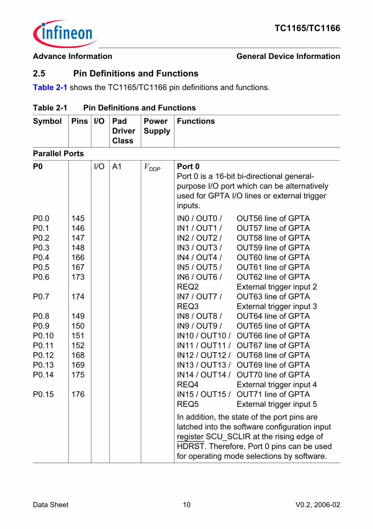
2.5 Pin Definitions and FunctionsTable 2-1 shows the TC1165/TC1166 pin definitions and functions.
Table 2-1 Pin Definitions and Functions Symbol Pins I/O Pad
Driver Class
PowerSupply
Functions
Parallel PortsP0 I/O A1 VDDP Port 0
Port 0 is a 16-bit bi-directional general- purpose I/O port which can be alternatively used for GPTA I/O lines or external trigger inputs.
P0.0P0.1P0.2P0.3P0.4P0.5P0.6
P0.7
P0.8P0.9P0.10P0.11P0.12P0.13P0.14
P0.15
145146147148166167173
174
149150151152168169175
176
IN0 / OUT0 /IN1 / OUT1 /IN2 / OUT2 /IN3 / OUT3 /IN4 / OUT4 /IN5 / OUT5 /IN6 / OUT6 /REQ2IN7 / OUT7 /REQ3IN8 / OUT8 /IN9 / OUT9 /IN10 / OUT10 /IN11 / OUT11 /IN12 / OUT12 /IN13 / OUT13 /IN14 / OUT14 /REQ4IN15 / OUT15 /REQ5
OUT56 line of GPTAOUT57 line of GPTAOUT58 line of GPTAOUT59 line of GPTAOUT60 line of GPTAOUT61 line of GPTAOUT62 line of GPTAExternal trigger input 2OUT63 line of GPTAExternal trigger input 3OUT64 line of GPTAOUT65 line of GPTAOUT66 line of GPTAOUT67 line of GPTAOUT68 line of GPTAOUT69 line of GPTAOUT70 line of GPTAExternal trigger input 4OUT71 line of GPTAExternal trigger input 5
In addition, the state of the port pins are latched into the software configuration input register SCU_SCLIR at the rising edge of HDRST. Therefore, Port 0 pins can be used for operating mode selections by software.
Data Sheet 10 V0.2, 2006-02

TC1165/TC1166
General Device InformationAdvance Information
P1 I/O VDDP Port 1Port 1 is a 15-bit bi-directional general purpose I/O port which can be alternatively used for GPTA I/O lines, SSC1 and ADC0 interface.
P1.0P1.1P1.2P1.3P1.4P1.5P1.6P1.7P1.8
P1.9
P1.10
P1.11
P1.12
P1.13
P1.14
9192939810710810911094
95
96
97
73
72
71
A1A1A1A1A1A1A1A1A2
A2
A2
A2
A1
A1
A1
IN16 / OUT16 /IN17 / OUT17 /IN18 / OUT18 /IN19 / OUT19 /IN20 / OUT20 /IN21 / OUT21 /IN22 / OUT22 /IN23 / OUT23 /IN24 / OUT24 /MTSR1B
IN25 / OUT25 /MRST1B
IN26 / OUT26 /SLSO17IN27 / OUT27 /SCLK1BAD0EMUX0
AD0EMUX1
AD0EMUX2
OUT72 line of GPTAOUT73 line of GPTAOUT74 line of GPTAOUT75 line of GPTAOUT76 line of GPTAOUT77 line of GPTAOUT78 line of GPTAOUT79 line of GPTAIN48 / OUT48 line of GPTASSC1 master transmit output / slave rec. input BIN49 / OUT49 line of GPTASSC1 master receive input / slave transmit output BIN50 / OUT50 line of GPTASSC1 slave select output 7IN51 / OUT51 line of GPTASSC1 clock input / output BADC0 external multiplexer control output 0ADC0 external multiplexer control output 1ADC0 external multiplexer control output 2
In addition, P1.4 also serves as emergency shut-off input for certain I/O lines (e.g. GPTA related outputs).
Table 2-1 Pin Definitions and Functions (cont’d)
Symbol Pins I/O Pad Driver Class
PowerSupply
Functions
Data Sheet 11 V0.2, 2006-02

TC1165/TC1166
General Device InformationAdvance Information
P2 I/O VDDP Port 2Port 2 is a 14-bit bi-directional general- purpose I/O port which can be alternatively used for GPTA I/O, and interface for MLI0, MSC0 or SSC0/1.
P2.0
P2.1
P2.2
P2.3
P2.4
P2.5
P2.6
P2.7
74
75
76
77
78
79
80
81
A2
A2
A2
A2
A1
A2
A1
A1
TCLK0A
IN32 / OUT32TREADY0A
IN33 / OUT33SLSO03SLSO13TVALID0A
IN34 / OUT34TDATA0A
IN35 / OUT35RCLK0A
IN36 / OUT36RREADY0A
IN37 / OUT37RVALID0A
IN38 / OUT38RDATA0A
IN39 / OUT39
MLI0 transmit channel clock output Aline of GPTAMLI0 transmit channel ready input Aline of GPTASSC0 slave select output 3SSC1 slave select output 3MLI0 transmit channel valid output Aline of GPTAMLI0 transmit channel data output Aline of GPTAMLI0 receive channel clock input Aline of GPTAMLI0 receive channel ready output Aline of GPTAMLI0 receive channel valid input Aline of GPTAMLI0 receive channel data input Aline of GPTA
Table 2-1 Pin Definitions and Functions (cont’d)
Symbol Pins I/O Pad Driver Class
PowerSupply
Functions
Data Sheet 12 V0.2, 2006-02

TC1165/TC1166
General Device InformationAdvance Information
P2.8
P2.9
P2.10
P2.11
P2.12
P2.13
164
160
161
162
163
165
A2
A2
A2
A2
A2
A1
SLSO04SLSO14EN00SLSO05SLSO15EN01MRST1A
SCLK1AFCLP0BMTSR1A
SOP0BSLSI1SDI0
SSC0 Slave Select output 4SSC1 Slave Select output 4MSC0 enable output 0SSC0 Slave Select output 5SSC1 Slave Select output 5MSC0 enable output 1SSC1 master receive input / slave transmit output ASSC1 clock input/output AMSC0 clock output BSSC1 master transmit out / slave receive input AMSC0 serial data output BSSC1 slave select inputMSC0 serial data input
Table 2-1 Pin Definitions and Functions (cont’d)
Symbol Pins I/O Pad Driver Class
PowerSupply
Functions
Data Sheet 13 V0.2, 2006-02

TC1165/TC1166
General Device InformationAdvance Information
P3 I/O VDDP Port 3Port 3 is a 16-bit bi-directional general- purpose I/O port which can be alternatively used for ASC0/1, SSC0/1 and CAN lines.
P3.0P3.1
136135
A2A2
RXD0ATXD0A
ASC0 receiver inp./outp. AASC0 transmitter output A
This pin is sampled at the rising edge of PORST. If this pin and the BYPASS input pin are both active, then oscillator bypass mode is entered.
P3.2P3.3
P3.4
P3.5
P3.6
P3.7
P3.8
P3.9P3.10P3.11P3.12
P3.13
P3.14
P3.15
129130
132
126
127
131
128
138137144143
142
134
133
A2A2
A2
A2
A2
A2
A2
A2A1A1A2
A2
A2
A2
SCLK0MRST0
MTSR0
SLSO00SLSO10SLSO01SLSO11SLSI0SLSO02SLSO12SLSO06TXD1ARXD1AREQ0REQ1RXDCAN01)
RXD0BTXDCAN01)
TXD0BRXDCAN11)
RXD1BTXDCAN11)
TXD1B
SSC0 clock input/outputSSC0 master receive input/ slave transmit outputSSC0 master transmit output/slave receive inputSSC0 slave select output 0SSC1 slave select output 0 2)
SSC0 slave select output 1SSC1 slave select output 12)
SSC0 slave select inputSSC0 slave select output 2SSC1 slave select output 2SSC0 slave select output 6ASC1 transmitter output AASC1 receiver inp./outp. AExternal trigger input 0External trigger input 1CAN node 0 receiver inputASC0 receiver inp./outp. BCAN node 0 transm. outputASC0 transmitter output BCAN node 1 receiver inputASC1 receiver inp./outp. BCAN node 1 transm. outputASC1 transmitter output B
Table 2-1 Pin Definitions and Functions (cont’d)
Symbol Pins I/O Pad Driver Class
PowerSupply
Functions
Data Sheet 14 V0.2, 2006-02

TC1165/TC1166
General Device InformationAdvance Information
P4 I/O VDDP Port 4 / Hardware Configuration InputsP4.[3:0] HWCFG[3:0] Boot mode and boot location
inputs; inputs are latched with the rising edge of HDRST.
During normal operation, Port 4 pins may be used as alternate functions for GPTA or system clock output.
P4.0P4.1P4.2P4.3
86878890
A1A1A2A2
IN28 / OUT28 /IN29 / OUT29 /IN30 / OUT30 /IN31 / OUT31 /SYSCLK
IN52 / OUT52 line of GPTAIN53 / OUT53 line of GPTAIN54 / OUT54 line of GPTAIN55 / OUT55 line of GPTASystem Clock Output
Table 2-1 Pin Definitions and Functions (cont’d)
Symbol Pins I/O Pad Driver Class
PowerSupply
Functions
Data Sheet 15 V0.2, 2006-02

TC1165/TC1166
General Device InformationAdvance Information
P5 I/O A2 VDDP Port 5Port 5 is a 16-bit bi-directional general- purpose I/O port. In emulation, it is used as a trace port for OCDS Level 2 debug lines. In normal operation, it is used for GPTA I/O or the MLI0/1 interface.
P5.0
P5.1
P5.2
P5.3
P5.4
P5.5
P5.6
P5.7
1
2
3
4
5
6
7
8
OCDSDBG0
IN40 / OUT40OCDSDBG1
IN41 / OUT41OCDSDBG2
IN42 / OUT42OCDSDBG3
IN43 / OUT43OCDSDBG4
IN44 / OUT44OCDSDBG5
IN45 / OUT45OCDSDBG6
IN46 / OUT46OCDSDBG7
IN47 / OUT47
OCDS L2 Debug Line 0 (Pipeline Status Sig. PS0)line of GPTAOCDS L2 Debug Line 1 (Pipeline Status Sig. PS1)line of GPTAOCDS L2 Debug Line 2 (Pipeline Status Sig. PS2)line of GPTAOCDS L2 Debug Line 3 (Pipeline Status Sig. PS3)line of GPTAOCDS L2 Debug Line 4 (Pipeline Status Sig. PS4)line of GPTAOCDS L2 Debug Line 5 (Break Qualification Line BRK0)line of GPTAOCDS L2 Debug Line 6 (Break Qualification Line BRK1)line of GPTAOCDS L2 Debug Line 7 (Break Qualification Line BRK2)line of GPTA
Table 2-1 Pin Definitions and Functions (cont’d)
Symbol Pins I/O Pad Driver Class
PowerSupply
Functions
Data Sheet 16 V0.2, 2006-02

TC1165/TC1166
General Device InformationAdvance Information
P5.8
P5.9
P5.10
P5.11
P5.12
P5.13
13
14
15
16
17
18
OCDSDBG8
TDATA1
RDATA0B
OCDSDBG9
TVALID1
RVALID0B
OCDSDBG10
TREADY1
RREADY0B
OCDSDBG11
TCLK1
RCLK0B
OCDSDBG12
RDATA1
TDATA0B
OCDSDBG13
RVALID1
TVALID0B
OCDS L2 Debug Line 8 (Indirect PC Addr. PC0)MLI1 transmit channel data outputMLI0 receive channel data input BOCDS L2 Debug Line 9 (Indirect PC Addr. PC1)MLI1 transmit channel valid outputMLI0 receive channel valid input BOCDS L2 Debug Line 10 (Indirect PC Addr. PC2)MLI1 transmit channel ready inputMLI0 receive channel ready output BOCDS L2 Debug Line 11 (Indirect PC Addr. PC3)MLI1 transmit channel clock outputMLI0 receive channel clock input BOCDS L2 Debug Line 12 (Indirect PC Addr. PC04)MLI1 receive channel data inputMLI0 transmit channel data output BOCDS L2 Debug Line 13 (Indirect PC Addr. PC05)MLI1 receive channel valid inputMLI0 transmit channel valid output B
Table 2-1 Pin Definitions and Functions (cont’d)
Symbol Pins I/O Pad Driver Class
PowerSupply
Functions
Data Sheet 17 V0.2, 2006-02

TC1165/TC1166
General Device InformationAdvance Information
P5.14
P5.15
19
20
OCDSDBG14
RREADY1
TREADY0B
OCDSDBG15
RCLK1
TCLK0B
OCDS L2 Debug Line 14 (Indirect PC Address PC6)MLI1 receive channel ready outputMLI0 transmit channel ready input BOCDS L2 Debug Line 15 (Indirect PC Address PC7)MLI1 receive channel clock inputMLI0 transmit channel clock output B
MSC0 Outputs
FCLP0A
FCLN0
SOP0A
SON0
157
156
159
158
O
O
O
O
C VDDP LVDS MSC Clock and Data Outputs4)
MSC0 Differential Driver Clock Output Positive AMSC0 Differential Driver Clock Output NegativeMSC0 Differential Driver Serial Data Output Positive AMSC0 Differential Driver Serial Data Output Negative
Table 2-1 Pin Definitions and Functions (cont’d)
Symbol Pins I/O Pad Driver Class
PowerSupply
Functions
Data Sheet 18 V0.2, 2006-02

TC1165/TC1166
General Device InformationAdvance Information
Analog InputsAN[35:0]
AN0AN1AN2AN3AN4AN5AN6AN7AN8AN9AN10AN11AN12AN13AN14AN15AN16AN17AN18AN19AN20AN21AN22AN23AN24AN25AN26AN27AN28AN29AN30
67666564636261366059585756555049484746454443424140393837353433
I D – Analog Input PortThe Analog Input Port provides altogether 36 analog input lines to ADC0 and FADC.AN[31:0]: ADC0 analog inputs [31:0]AN[35:32]: FADC analog differential inputsAnalog input 0Analog input 1Analog input 2Analog input 3Analog input 4Analog input 5Analog input 6Analog input 7Analog input 8Analog input 9Analog input 10Analog input 11Analog input 12Analog input 13Analog input 14Analog input 15Analog input 16Analog input 17Analog input 18Analog input 19Analog input 20Analog input 21Analog input 22Analog input 23Analog input 24Analog input 25Analog input 26Analog input 27Analog input 28Analog input 29Analog input 30
Table 2-1 Pin Definitions and Functions (cont’d)
Symbol Pins I/O Pad Driver Class
PowerSupply
Functions
Data Sheet 19 V0.2, 2006-02

TC1165/TC1166
General Device InformationAdvance Information
AN31AN32AN33AN34AN35
3231302928
I D – Analog input 31Analog input 32Analog input 33Analog input 34Analog input 35
System I/OTRST 114 I A23) VDDP JTAG Module Reset/Enable InputTCK 115 I A23) VDDP JTAG Module Clock InputTDI 111 I A13) VDDP JTAG Module Serial Data InputTDO 113 O A2 VDDP JTAG Module Serial Data OutputTMS 112 I A23) VDDP JTAG Module State Machine Control InputBRKIN 117 I/O A3 VDDP OCDS Break Input (Alternate Output)4)5)
BRK OUT
116 I/O A3 VDDP OCDS Break Output (Alternate Input)4)5)
TRCLK 9 O A4 VDDP Trace Clock for OCDS_L2 Lines4)
NMI 120 I A26)7) VDDP Non-Maskable Interrupt InputHDRST 122 I/O A28) VDDP Hardware Reset Input /
Reset Indication OutputPORST 9)
121 I A26)7) VDDP Power-on Reset Input
BYPASS 119 I A13) VDDP PLL Clock Bypass Select InputThis input has to be held stable during power-on resets. With BYPASS = 1, the spike filters in the HDRST, PORST and NMI inputs are switched off.
TEST MODE
118 I A26)10) VDDP Test Mode Select InputFor normal operation of the TC1165/TC1166, this pin should be connected to high level.
XTAL1 XTAL2
102103
I O
n.a. VDDOSC Oscillator/PLL/Clock Generator Input/Output Pins
Table 2-1 Pin Definitions and Functions (cont’d)
Symbol Pins I/O Pad Driver Class
PowerSupply
Functions
Data Sheet 20 V0.2, 2006-02

TC1165/TC1166
General Device InformationAdvance Information
N.C. 21, 89
– – – Not ConnectedThese pins are reserved for future extension and must not be connected externally.
Power SuppliesVDDM 54 – – – ADC Analog Part Power Supply (3.3 V)VSSM 53 – – – ADC Analog Part Ground for VDDM
VDDMF 24 – – – FADC Analog Part Power Supply (3.3 V)VSSMF 25 – – – FADC Analog Part Ground for VDDMF
VDDAF 23 – – – FADC Analog Part Logic Power Supply (1.5 V)
VSSAF 22 – – – FADC Analog Part Logic Ground for VDDAF
VAREF0 52 – – – ADC Reference VoltageVAGND0 51 – – – ADC Reference GroundVFAREF 26 – – – FADC Reference VoltageVFAGND 27 – – – FADC Reference GroundVDDOSC 105 – – – Main Oscillator and PLL Power Supply
(1.5 V)VDDOSC3 106 – – – Main Oscillator Power Supply (3.3 V)VSSOSC 104 – – – Main Oscillator and PLL GroundVDDFL3 141 – – – Power Supply for Flash (3.3 V)VDD 10,
68, 84, 99, 123, 153, 170
– – – Core Power Supply (1.5 V)
Table 2-1 Pin Definitions and Functions (cont’d)
Symbol Pins I/O Pad Driver Class
PowerSupply
Functions
Data Sheet 21 V0.2, 2006-02

TC1165/TC1166
General Device InformationAdvance Information
VDDP 11, 69, 83, 100, 124, 154, 171, 139
– – – Port Power Supply (3.3 V)
VSS 12, 70, 85, 101, 125, 155, 172, 140, 82
– – – Ground
1) Not applicable to TC11652) The logical AND function of the two slave select outputs is available as a third alternate output function.3) These pads are I/O pads with input only function. Its input characteristics are identical with the input
characteristics as defined for class A pads.4) In case of a power-fail condition (one or more power supply voltages drop below the specified voltage range),
an undefined output driving level may occur at these pins.5) Programmed by software as either break input or break output.6) These pads are input only pads with input characteristics.7) Input only pads with input spike filter.8) Open drain pad with input spike filter.9) The dual input reset system of TC1165/TC1166 assumes that the PORST reset pin is used for power on reset
only.10) Input only pads without input spike filter.
Table 2-1 Pin Definitions and Functions (cont’d)
Symbol Pins I/O Pad Driver Class
PowerSupply
Functions
Data Sheet 22 V0.2, 2006-02

TC1165/TC1166
General Device InformationAdvance Information
Table 2-2 List of Pull-up/Pull-down Reset Behavior of the Pins Pins PORST = 0 PORST = 1All GPIOs, TDI, TMS, TDO Pull-upHDRST Drive-low Pull-upBYPASS Pull-up High-impedanceTRST, TCK High-impedance Pull-downTRCLK High-impedanceBRKIN, BRKOUT, TESTMODE Pull-upNMI, PORST Pull-down
Data Sheet 23 V0.2, 2006-02

TC1165/TC1166
Functional DescriptionAdvance Information
3 Functional DescriptionChapter 3 provides an overview of the TC1165/TC1166 functional description.
3.1 System Architecture and On-Chip Bus SystemsThe TC1165/TC1166 has two independent on-chip buses (see also TC1165/TC1166block diagram on Page 2-6):• Local Memory Bus (LMB)• System Peripheral Bus (SPB)The LMB Bus connects the CPU local resources for data and instruction fetch. The LocalMemory Bus interconnects the memory units and functional units, such as CPU andPMU. The main target of the LMB bus is to support devices with fast response times,optimized for speed. This allows the DMI and PMI fast access to local memory andreduces load on the FPI bus. The Tricore system itself is located on LMB bus.The Local Memory Bus is a synchronous, pipelined, split bus with variable block sizetransfer support. It supports 8-, 16-, 32- and 64-bit single transactions and variablelength 64-bit block transfers.The SPB Bus is mainly governed by the PCP and is accessible to the CPU via the LMBBus bridge. The System Peripheral Bus (SPB Bus) in TC1165/TC1166 is an on-chip FPIBus. The FPI Bus interconnects the functional units of the TC1165/TC1166, such as theDMA and on-chip peripheral components. The FPI Bus is designed to be quick to beacquired by on-chip functional units, and quick to transfer data. The low setup overheadof the FPI Bus access protocol guarantees fast FPI Bus acquisition, which is required fortime-critical applications.The FPI Bus is designed to sustain high transfer rates. Forexample, a peak transfer rate of up to 320 Mbyte/s can be achieved with a 80 MHz busclock and 32-bit data bus. Multiple data transfers per bus arbitration cycle allow the FPIBus to operate at close to its peak bandwidth.Both the LMB Bus and the SPB Bus runs at full CPU speed. The maximum CPU speedis 80 MHz.Additionally, two simplified bus interfaces are connected to and controlled by the DMAController:• DMA Bus• SMIF Interface
Data Sheet 24 V0.2, 2006-02

TC1165/TC1166
Functional DescriptionAdvance Information
3.2 On-Chip MemoriesAs shown in the TC1165/TC1166 block diagram on Page 2-6, some of theTC1165/TC1166 units provide on-chip memories that are used as program or datamemory.• Program memory in PMU
– 16 Kbyte Boot ROM (BROM)– 1504 Kbyte Program Flash (PFlash)
• Program memory in PMI– 16 Kbyte Scratch-Pad RAM (SPRAM)– 8 Kbyte Instruction Cache (ICACHE)
• Data memory in PMU– 32 Kbyte Data Flash (DFlash)– 8 Kbyte Overlay RAM (OVRAM)
• Data memory in DMI– 56 Kbyte Local Data RAM (LDRAM)
• Memory of PCP2– 12 Kbyte Code Memory (CMEM) with parity error protection– 8 Kbyte Parameter RAM (PRAM) with parity error protection
• On-chip SRAM with parity error protection
Features of Program Flash• 1504 Kbyte on-chip program Flash memory• Usable for instruction code or constant data storage• 256-byte program interface
– 256 bytes are programmed into PFLASH page in one step/command• 256-bit read interface
– Transfer from PFLASH to CPU/PMI by four 64-bit single cycle burst transfers• Dynamic correction of single-bit errors during read access• Detection of double-bit errors• Fixed sector architecture
– Eight 16 Kbyte, one 128 Kbyte, one 256 Kbyte, one 512 Kbyte and one 480 Kbytesectors
– Each sector separately erasable– Each sector separately write-protectable
• Configurable read protection for complete PFLASH with sophisticated read accesssupervision, combined with write protection for complete PFLASH (protection against“Trojan horse” software)
• Configurable write protection for each sector– Each sector separately write-protectable– With capability to be re-programmed– With capability to be locked forever (OTP)
• Password mechanism for temporary disabling of write and read protection
Data Sheet 25 V0.2, 2006-02

TC1165/TC1166
Functional DescriptionAdvance Information
• On-chip generation of programming voltage• JEDEC-standard based command sequences for PFLASH control
– Write state machine controls programming and erase operations– Status and error reporting by status flags and interrupt
• Margin check for detection of problematic PFLASH bits
Features of Data Flash• 32 Kbyte on-chip data Flash memory, organized in two 16 Kbyte banks• Usable for data storage with EEPROM functionality• 128 Byte of program interface
– 128 bytes are programmed into one DFLASH page by one step/command• 64-bit read interface (no burst transfers)• Dynamic correction of single-bit errors during read access• Detection of double-bit errors• Fixed sector architecture
– Two 16 Kbyte banks/sectors– Each sector separately erasable
• Configurable read protection (combined with write protection) for complete DFLASHtogether with PFLASH read protection
• Password mechanism for temporary disabling of write and read protection• Erasing/programming of one bank possible while reading data from the other bank• Programming of one bank while erasing the other bank possible• On-chip generation of programming voltage• JEDEC-standard based command sequences for DFLASH control
– Write state machine controls programming and erase operations– Status and error reporting by status flags and interrupt
• Margin check for detection of problematic DFLASH bits
Data Sheet 26 V0.2, 2006-02

TC1165/TC1166
Functional DescriptionAdvance Information
3.3 Memory MapsThis chapter gives an overview of the TC1165/TC1166 memory map and describes theaddress locations and access possibilities for the units, memories, and reserved areasas “seen” from different on-chip buses’ (SPB and LMB) point of view.
3.3.1 Architectural Address MapTable 3-1 shows the overall architectural address map as defined for the TriCore and asimplemented in TC1165/TC1166.
Table 3-1 TC1165/TC1166 Architectural Address MapSeg-ment
Contents Size Description
0-7 Global 8 x 256 Mbyte
Reserved (MMU space); cached
8 Global Memory
256 Mbyte Reserved (246 Mbyte); PMU, Boot ROM; cached
9 Global Memory
256 Mbyte FPI space; cached
10 Global Memory
256 Mbyte Reserved (246 Mbyte), PMU, Boot ROM; non-cached
11 Global Memory
256 Mbyte FPI space; non-cached
12 Local LMB Memory
256 Mbyte Reserved; bottom 4 Mbyte visible from FPI bus in segment 14; cached
13 DMI 64 Mbyte Local Data Memory RAM; non-cachedPMI 64 Mbyte Local Code Memory RAM; non-cachedEXT_PER 96 Mbyte Reserved; non-cachedEXT_EMU 16 Mbyte Reserved; non-cachedBOOTROM 16 Mbyte Boot ROM space, Boot ROM mirror;
non-cached
Data Sheet 27 V0.2, 2006-02

TC1165/TC1166
Functional DescriptionAdvance Information
14 EXTPER 128 Mbyte Reserved; non-speculative; non-cached; no execution
CPU[0 ..15]image region
16 x 8 Mbyte
Non-speculative; non-cached; no execution
15 LMB_PERCSFRsINT_PER
256Mbyte
CSFRs of CPUs[0 ..15];LMB & FPI Peripheral Space;non-speculative; non-cached;no execution
Table 3-1 TC1165/TC1166 Architectural Address Map (cont’d)
Seg-ment
Contents Size Description
Data Sheet 28 V0.2, 2006-02
TC1165/TC1166
Functional DescriptionAdvance Information
3.3.2 How to Read the Address MapsThe bus-specific address maps describe how the different bus master devices react onaccesses to on-chip memories and modules, and which address ranges are valid orinvalid for the corresponding buses.The FPI Bus address map shows the system addresses from the point of view of theSPB master agents. SPB master agents are PCP2 and OCDS, and DMA.The LMB address map shows the system addresses from the point of view of the LMBmaster agents. LMB master agents are PMI and DMI.Table 3-2 defines the acronyms and other terms that are used in the address maps(Table 3-3 to Table 3-5).
Table 3-2 Definition of Acronyms and TermsTerm Description…BE Means “Bus error” generation.…BET Means “Bus error & trap” generation.SPBBE A bus access is terminated with a bus error on the SPB.SPBBET A bus access is terminated with a bus error on the SPB and a DSE
trap (read access) or DAE trap (write access).LMBBE A bus access is terminated with a bus error on the LMB.LMBBET A bus access is terminated with a bus error on the LMB and a DSE
trap (read access) or DAE trap (write access).access A bus access is allowed and is executed.ignore A bus access is ignored and is not executed. No bus error is
generated.trap A DSE trap (read access) or DAE trap (write access) is generated.32 Only 32-bit word bus accesses are permitted to that
register/address range.nE A bus access generates no bus error, although the bus access
points to an undefined address or address range. This is valid e.g. for CPU accesses (MTCR/MFCR) to undefined addresses in the CSFR range.
Data Sheet 29 V0.2, 2006-02

TC1165/TC1166
Functional DescriptionAdvance Information
3.3.3 Contents of the SegmentsThis section summarizes the contents of the segments.
Segments 0-7These segments are reserved segments in the TC1165/TC1166.
Segment 8From the SPB point of view (PCP, DMA and Cerberus), this memory segment allowsaccesses to all PMU memories (PFLASH, DFLASH, BROM, and TROM).From the CPU point of view (PMI and DMI), this memory segment allows cachedaccesses to all PMU memories (PFLASH, DFLASH, BROM, and TROM).
Segment 9This memory segment is reserved in the TC1165/TC1166.
Segment 10From the SPB point of view (PCP, DMA and Cerberus), this memory segment allowsaccesses to all PMU memories (PFLASH, DFLASH, BROM, and TROM).From the CPU point of view (PMI and DMI), this memory segment allows non-cachedaccesses to all PMU memories (PFLASH, DFLASH, BROM, and TROM).
Segment 11This memory segment is reserved in the TC1165/TC1166.
Segment 12From the SPB point of view (PCP, DMA, and Cerberus), this memory segment isreserved in the TC1165/TC1166.From the CPU point of view (PMI and DMI), this memory segment allows cachedaccesses to the PMU memory, OVRAM.
Segment 13From the SPB point of view (PCP, DMA and Cerberus), this memory segment isreserved in the TC1165/TC1166.From the CPU point of view (PMI and DMI), this memory segment allows non-cachedaccesses to the PMI scratch-pad RAM, read access to the boot ROM and test ROM(BROM and TROM) and the DMI memories (LDRAM).
Data Sheet 30 V0.2, 2006-02

TC1165/TC1166
Functional DescriptionAdvance Information
Segment 14From the SPB point of view (PCP, DMA and Cerberus), this memory segment allowsaccesses to the PMU Overlay memory (OVRAM), the DMI Local Data RAM (LDRAM),and the PMI scratch-pad RAM (SPRAM).From the CPU point of view (PMI and DMI), this memory segment is reserved in theTC1165/TC1166.
Segment 15From the SPB point of view (PCP, DMA and Cerberus), this memory segment allowsaccesses to all SFRs and CSFRs, the PCP memories, and the MLI transfer windows.From the CPU point of view (PMI and DMI), this memory segment allows accesses to allSFRs and CSFRs, the PCP memories, and the MLI transfer windows.
Data Sheet 31 V0.2, 2006-02

TC1165/TC1166
Functional DescriptionAdvance Information
3.3.4 Address Map of the FPI Bus SystemTable 3-3 and Table 3-4 shows the address maps of the FPI Bus System.
3.3.4.1 Segments 0 to 14Table 3-3 shows the address maps of segments 0 to 14 as it is seen from the SPB busmasters PCP, DMA and OCDS.
Table 3-3 SPB Address Map of Segment 0 to 14Seg-ment
Address Range
Size Description Access TypeRead Write
0-7 0000 0000H - 0000 0007H
8 byte Reserved (virtual address space)
MPN trap MPN trap
0000 0008H - 7FFF FFFFH
8 × 256 Mbyte
SPBBE SPBBE
8 8000 0000H - 8017 7FFFH
1.5 Mbyte Program Flash (PFLASH) access access1)
8017 8000H - 807F FFFFH
6.5 Mbyte Reserved LMBBE & SPBBE
LMBBE
8080 0000H - 8FDF FFFFH
246 Mbyte
Reserved LMBBE & SPBBE
LMBBE
8FE0 0000H - 8FE0 3FFFH
16 Kbyte Data Flash (DFLASH)Bank 0
access access1)
8FE0 4000H - 8FE0 FFFFH
48 Kbyte Reserved LMBBE & SPBBE
LMBBE
8FE1 0000H - 8FE1 3FFFH
16 Kbyte Data Flash (DFLASH)Bank 1
access access1)
8FE1 4000H - 8FF1 FFFFH
1 Mbyte Reserved LMBBE & SPBBE
LMBBE
8FF2 0000H - 8FF5 FFFFH
256 Kbyte
Reserved
8FF6 0000H - 8FFF BFFFH
624 Kbyte
Reserved
8FFF C000H - 8FFF FFFFH
16 Kbyte Boot ROM (BROM) access
9 9000 0000H - 9FFF FFFFH
256 Mbyte
Reserved SPBBE SPBBE
Data Sheet 32 V0.2, 2006-02

TC1165/TC1166
Functional DescriptionAdvance Information
10 A000 0000H - A017 FFFFH
1.5 Mbyte Program Flash (PFLASH) access access1)
A017 8000H - A07F FFFFH
6.5 Mbyte Reserved LMBBE & SPBBE
LMBBE
A080 0000H - AFDF FFFFH
246 Mbyte
Reserved LMBBE & SPBBE
LMBBE
AFE0 0000H - AFE0 3FFFH
16 Kbyte Data Flash (DFLASH)Bank 0
access access1)
AFE0 4000H - AFE0 FFFFH
48 Kbyte Reserved LMBBE & SPBBE
LMBBE
AFE1 0000H - AFE1 3FFFH
16 Kbyte Data Flash (DFLASH)Bank 1
access access1)
AFE1 4000H - AFF1 FFFFH
1 Mbyte Reserved LMBBE & SPBBE
ignore
AFF2 0000H - AFF5 FFFFH
256 Kbyte
Reserved
AFF6 0000H - AFFF BFFFH
624 Kbyte
Reserved
AFFF C000H - AFFF FFFFH
16 Kbyte Boot ROM (BROM) access
11 B000 0000H - BFFF FFFFH
256 Mbyte
Reserved SPBBE SPBBE
12 C000 0000H - C000 1FFFH
8 Kbyte Overlay memory (OVRAM)
SPBBE SPBBE
C000 2000H - CFFF FFFFH
≈ 256 Mbyte
Reserved SPBBE SPBBE
Table 3-3 SPB Address Map of Segment 0 to 14 (cont’d)
Seg-ment
Address Range
Size Description Access TypeRead Write
Data Sheet 33 V0.2, 2006-02

TC1165/TC1166
Functional DescriptionAdvance Information
13 D000 0000H - D000 DFFFH
56 Kbyte DMI Local Data RAM (LDRAM)
SPBBE SPBBE
D000 E000H - D3FF FFFFH
64 Mbyte Reserved SPBBE SPBBE
D400 0000H - D400 3FFFH
16 Kbyte PMI Scratch-Pad RAM (SPRAM)
SPBBE SPBBE
D400 4000H - D7FF FFFFH
64 Mbyte Reserved SPBBE SPBBE
D800 0000H - DEFF FFFFH
112 Mbyte
Reserved SPBBE SPBBE
DF00 0000H - DFFF FFEFH
≈ 16 Mbyte
Reserved (for Boot Rom) SPBBE SPBBE
DFFF FFF0H - DFFF FFFFH
16 byte microROM SPBBE SPBBE
14 E000 0000H - E7FF FFFFH
128 MB Reserved LMBBE LMBBE
E800 0000H - E800 1FFFH
8 Kbyte Overlay memory (OVRAM)
access access
E800 2000H - E83F FFFFH
≈ 4 Mbyte
Reserved LMBBE LMBBE
E840 0000H - E840 DFFFH
56 Kbyte DMI Local Data RAM (LDRAM)
access access
E840 E000H - E84F FFFFH
≈ 1 Mbyte Reserved LMBBE LMBBE
E850 0000H - E850 3FFFH
16 Kbyte PMI Scratch-Pad RAM (SPRAM)
access access
E850 4000H - E85F FFFFH
≈ 1 Mbyte Reserved LMBBE LMBBE
E860 C000H - EFFF FFFFH
≈ 122 Mbyte
Reserved LMBBE LMBBE
15 F000 0000H - FFFF FFFFH
256 Mbyte
see Table 3-4
1) Only applicable when writing Flash command sequences.
Table 3-3 SPB Address Map of Segment 0 to 14 (cont’d)
Seg-ment
Address Range
Size Description Access TypeRead Write
Data Sheet 34 V0.2, 2006-02

TC1165/TC1166
Functional DescriptionAdvance Information
3.3.4.2 Segment 15Table 3-4 shows the address map of segment 15 as seen from the SPB bus mastersPCP, DMA and OCDS. Please note that access in Table 3-4 means only that an accessto an address within the defined address range is not automatically incorrect or ignored.If an access is really addressing a correct address, it can be found in the detailed tablesin the TC116x User’s Manual, Register Overview’s chapter.
Table 3-4 SPB Address Map of Segment 15Unit Address
RangeSize Access Type
Read WriteSystem Control Unit (SCU) and Watchdog Timer (WDT)
F000 0000H - F000 00FFH
256 byte
access access
System Peripheral Bus Control Unit (SBCU)
F000 0100H - F000 01FFH
256 byte
access access
System Timer (STM) F000 0200H - F000 02FFH
256 byte
access access
Reserved F000 0300H - F000 03FFH
– SPBBE SPBBE
On-Chip Debug Support (Cerberus) F000 0400H - F000 04FFH
256 byte
access access
Reserved F000 0500H - F000 07FFH
– SPBBE SPBBE
MicroSecond Bus Controller 0 (MSC0)
F000 0800H - F000 08FFH
256 byte
access access
Reserved F000 0900H - F000 09FFH
– SPBBE SPBBE
Async./Sync. Serial Interface 0 (ASC0)
F000 0A00H - F000 0AFFH
256 byte
access access
Async./Sync. Serial Interface 1 (ASC1)
F000 0B00H - F000 0BFFH
256 byte
access access
Port 0 F000 0C00H - F000 0CFFH
256 byte
access access
Port 1 F000 0D00H - F000 0DFFH
256 byte
access access
Port 2 F000 0E00H - F000 0EFFH
256 byte
access access
Data Sheet 35 V0.2, 2006-02

TC1165/TC1166
Functional DescriptionAdvance Information
Port 3 F000 0F00H - F000 0FFFH
256 byte
access access
Port 4 F000 1000H - F000 10FFH
256 byte
access access
Port 5 F000 1100H - F000 11FFH
256 byte
access access
Reserved F000 1200H - F000 12FFH
– SPBBE SPBBE
Reserved F000 1300H - F000 13FFH
– SPBBE SPBBE
Reserved F000 1400H - F000 14FFH
– SPBBE SPBBE
Reserved F000 1500H - F000 15FFH
– SPBBE SPBBE
Reserved F000 1600H - F000 16FFH
– SPBBE SPBBE
Reserved F000 1700H - F000 17FFH
– SPBBE SPBBE
General Purpose Timer Array 0 (GPTA0)
F000 1800H - F000 1FFFH
8 × 256 byte
access access
Reserved F000 2000H - F000 27FFH
– SPBBE SPBBE
Reserved F000 2800H - F000 2FFFH
– SPBBE SPBBE
Reserved F000 3000H - F000 3BFFH
– SPBBE SPBBE
Direct Memory Access Controller (DMA)
F000 3C00H - F000 3EFFH
3 × 256 byte
access access
Reserved F000 3F00H - F000 3FFFH
– SPBBE SPBBE
MultiCAN Controller (CAN) F000 4000H - F000 5FFFH
8 Kbyte access1) access1)
Table 3-4 SPB Address Map of Segment 15 (cont’d)
Unit Address Range
Size Access TypeRead Write
Data Sheet 36 V0.2, 2006-02

TC1165/TC1166
Functional DescriptionAdvance Information
Reserved F000 6000H - F003 FFFFH
– SPBBE SPBBE
Reserved F004 0000H - F004 3EFFH
– SPBBE SPBBE
PCP Registers F004 3F00H - F004 3FFFH
256 byte
access access
Reserved F004 4000H - F004 FFFFH
– SPBBE SPBBE
PCP Data Memory (PRAM) F005 0000H - F005 1FFFH
8 Kbyte nE, 32 nE, 32
Reserved F005 2000H - F005 FFFFH
– SPBBE SPBBE
PCP Code Memory (PCODE) F006 0000H - F006 2FFFH
12 Kbyte
nE, 32 nE, 32
Reserved F006 3000H - F007 FFFFH
– SPBBE SPBBE
Reserved F008 0000H - F00F FFFFH
– SPBBE SPBBE
Reserved F010 0000H - F010 00FFH
– SPBBE SPBBE
Synchronous Serial Interface 0 (SSC0)
F010 0100H - F010 01FFH
256 byte
access access
Synchronous Serial Interface 1 (SSC1)
F010 0200H - F010 02FFH
256 byte
access access
Fast Analog-to-Digital Converter (FADC)
F010 0300H - F010 03FFH
256 byte
access access
Analog-to-Digital Converter 0 (ADC0)
F010 0400H - F010 05FFH
2 × 256 byte
access access
Reserved F010 0600H - F010 07FFH
– SPBBE SPBBE
Reserved F010 0800H - F010 9FFFH
– SPBBE SPBBE
Table 3-4 SPB Address Map of Segment 15 (cont’d)
Unit Address Range
Size Access TypeRead Write
Data Sheet 37 V0.2, 2006-02

TC1165/TC1166
Functional DescriptionAdvance Information
Reserved F010 A000H - F010 BFFFH
– SPBBE SPBBE
Micro Link Interface 0 (MLI0) F010 C000H - F010 C0FFH
256 byte
access access
Micro Link Interface 1(MLI1) F010 C100H - F010 C1FFH
256 byte
access access
Memory Checker (MCHK) F010 C200H - F010 C2FFH
256 byte
access access
Reserved F010 C300H - F01D FFFFH
– SPBBE SPBBE
MLI0 Small Transfer Windows F01E 0000H - F01E 7FFFH
4 × 8 Kbyte
access access
MLI1 Small Transfer Windows F01E 8000H - F01E FFFFH
4 × 8 Kbyte
access access
Reserved F01F 0000H - F01F FFFFH
– SPBBE SPBBE
MLI0 Large Transfer Windows F020 0000H - F023FFFFH
4 × 64 Kbyte
access access
MLI1 Large Transfer Windows F024 0000H - F027 FFFFH
4 × 64 Kbyte
access access
Reserved F028 0000H - F7E0 FEFFH
– SPBBE SPBBE
CPU CPU Slave Interface Registers (CPS)
F7E0 FF00H - F7E0 FFFFH
256 byte
access access
CPU Core SFRs & GPRs F7E1 0000H - F7E1 FFFFH
64 Kbyte
access access
Reserved F7E2 0000H - F7FF FFFFH
– SPBBE SPBBE
Reserved F800 0000H - F800 03FFH
– SPBBE SPBBE
Reserved F800 0400H - F800 04FFH
– LMBBE & SPBBE
LMBBE
Table 3-4 SPB Address Map of Segment 15 (cont’d)
Unit Address Range
Size Access TypeRead Write
Data Sheet 38 V0.2, 2006-02

TC1165/TC1166
Functional DescriptionAdvance Information
Program Memory Unit (PMU) F800 0500H - F800 05FFH
256 byte
access access
Reserved F800 0600H - F800 0FFFH
– LMBBE & SPBBE
LMBBE
Flash Register F800 1000H - F800 23FFH
5 Kbyte access access
Reserved F800 2400H - F801 00FFH
– LMBBE & SPBBE
LMBBE
Reserved F801 0100H - F801 01FFH
– LMBBE & SPBBE
LMBBE
Reserved F801 0200H - F87F F9FFH
– LMBBE & SPBBE
LMBBE
Reserved F87F FA00H - F87F FAFFH
– LMBBE & SPBBE
LMBBE
Reserved F87F FB00H - F87F FBFFH
– LMBBE & SPBBE
LMBBE
CPU DMI Registers F87F FC00H - F87F FCFFH
256 byte
access access
PMI Registers F87F FD00H - F87F FDFFH
256 byte
access access
Local Memory Bus Control Unit (LBCU)
F87F FE00H - F87F FEFFH
256 byte
access access
LFI Bridge F87F FF00H - F87F FFFFH
256 byte
access access
Reserved F880 0000H - FFFF FFFFH
– LMBBE & SPBBE
LMBBE
1) For TC1165, read and write accesses to this address range will not generate any traps.
Table 3-4 SPB Address Map of Segment 15 (cont’d)
Unit Address Range
Size Access TypeRead Write
Data Sheet 39 V0.2, 2006-02

TC1165/TC1166
Functional DescriptionAdvance Information
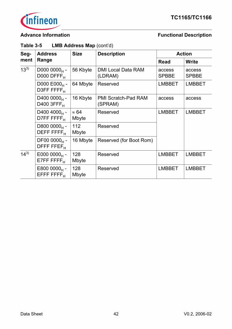
3.3.5 Address Map of the Local Memory Bus (LMB)Table 3-5 shows the address map as seen from the LMB bus masters (PMI and DMI).
Table 3-5 LMB Address MapSeg-ment
Address Range
Size Description ActionRead Write
0-71) 0000 0000H - 0000 0007H
8 byte Reserved (virtual address space)
MPN trap MPN trap
0000 0008H - 7FFF FFFFH
8 × 256 Mbyte
SPBBET SPBBE
81) 8000 0000H - 8017 7FFFH
1.5 Mbyte Program Flash (PFLASH) access access2)
8017 8000H - 807F FFFFH
6.5 Mbyte Reserved LMBBET LMBBET
8080 0000H - 8FDF FFFFH
246 Mbyte
Reserved LMBBET LMBBET
8FE0 0000H - 8FE0 3FFFH
16 Kbyte Data Flash (DFLASH)Bank 0
access access2)
8FE0 4000H - 8FE0 FFFFH
48 Kbyte Reserved LMBBET LMBBET
8FE1 0000H - 8FE1 3FFFH
16 Kbyte Data Flash (DFLASH)Bank 1
access access2)
8FE1 4000H - 8FF1 FFFFH
1 Mbyte Reserved LMBBET LMBBET
8FF2 0000H - 8FF5 FFFFH
256 Kbyte Reserved
8FF6 0000H - 8FFF BFFFH
624 Kbyte Reserved
8FFF C000H - 8FFF FFFFH
16 Kbyte Boot ROM (BROM) access
91) 9000 0000H - 9FFF FFFFH
256 Mbyte
Reserved SPBBET SPBBE
Data Sheet 40 V0.2, 2006-02

TC1165/TC1166
Functional DescriptionAdvance Information
103) A000 0000H - A017 FFFFH
1.5 Mbyte Program Flash (PFLASH) access access2)
A017 8000H - A07F FFFFH
6.5 Mbyte Reserved LMBBET LMBBET
A080 0000H - AFDF FFFFH
246 Mbyte
Reserved LMBBET LMBBET
AFE0 0000H - AFE0 3FFFH
16 Kbyte Data Flash (DFLASH)Bank 0
access access2)
AFE0 4000H - AFE0 FFFFH
48 Kbyte Reserved LMBBET LMBBET
AFE1 0000H - AFE1 3FFFH
16 Kbyte Data Flash (DFLASH)Bank 1
access access2)
AFE1 4000H - AFF1 FFFFH
1 Mbyte Reserved LMBBET LMBBET
AFF2 0000H - AFF5 FFFFH
256 Kbyte Reserved
AFF6 0000H - AFFF BFFFH
624 Kbyte Reserved
AFFF C000H - AFFF FFFFH
16 Kbyte Boot ROM (BROM) access
113) B000 0000H - BFFF FFFFH
256 Mbyte
Reserved SPBBET SPBBE
121) C000 0000H - C000 1FFFH
8 Kbyte Overlay memory (OVRAM)
access access
C000 2000H - CFFF FFFFH
256 Mbyte
Reserved LMBBET LMBBET
Table 3-5 LMB Address Map (cont’d)
Seg-ment
Address Range
Size Description ActionRead Write
Data Sheet 41 V0.2, 2006-02
TC1165/TC1166
Functional DescriptionAdvance Information
133) D000 0000H - D000 DFFFH
56 Kbyte DMI Local Data RAM (LDRAM)
access SPBBE
access SPBBE
D000 E000H - D3FF FFFFH
64 Mbyte Reserved LMBBET LMBBET
D400 0000H - D400 3FFFH
16 Kbyte PMI Scratch-Pad RAM (SPRAM)
access access
D400 4000H - D7FF FFFFH
≈ 64 Mbyte
Reserved LMBBET LMBBET
D800 0000H - DEFF FFFFH
112 Mbyte
Reserved
DF00 0000H - DFFF FFEFH
16 Mbyte Reserved (for Boot Rom)
143) E000 0000H - E7FF FFFFH
128 Mbyte
Reserved LMBBET LMBBET
E800 0000H - EFFF FFFFH
128 Mbyte
Reserved LMBBET LMBBET
Table 3-5 LMB Address Map (cont’d)
Seg-ment
Address Range
Size Description ActionRead Write
Data Sheet 42 V0.2, 2006-02

TC1165/TC1166
Functional DescriptionAdvance Information
15 F000 0000H - F7FF FFFFH
128 Mbyte
Address map is identical to FPI Bus segment 15 address map (see Table 3-5)Reserved areas give an bus error.
SPBBET SPBBE
F800 0000H - F800 03FFH
1 Kbyte Reserved LMBBET LMBBET
F800 0400H - F800 04FFH
256 byte Reserved LMBBET LMBBET
F800 0500H - F800 05FFH
256 byte Program Memory Unit (PMU)
access access
F800 0600H - F800 0FFFH
≈ 2 Kbyte Reserved LMBBET LMBBET
F800 1000H - F800 23FFH
5 Kbyte Flash Registers access access
F800 2400H - F87F FBFFH
≈ 8 Mbyte Reserved LMBBET LMBBET
F87F FC00H - F87F FCFFH
256 byte Data Memory Interface Unit
access access
F87F FD00H - F87F FDFFH
256 byte Program Memory Interface Unit
access access
F87F FE00H - F87F FEFFH
256 byte LBCU register space access access
F87F FF00H - F87F FFFFH
256 byte LFI Bus Bridge access access
F880 0000H - FFFF FFFFH
≈ 119 Mbyte
Reserved LMBBET LMBBET
1) Cached area2) Only applicable when writing Flash command sequences3) Non-cached area
Table 3-5 LMB Address Map (cont’d)
Seg-ment
Address Range
Size Description ActionRead Write
Data Sheet 43 V0.2, 2006-02

TC1165/TC1166
Functional DescriptionAdvance Information
3.4 Memory Protection SystemThe TC1165/TC1166 memory protection system specifies the addressable range andread/write permissions of memory segments available to the current executing task. Thememory protection system controls the position and range of addressable segments inmemory. It also controls the types of read and write operations allowed withinaddressable memory segments. Any illegal memory access is detected by the memoryprotection hardware, which then invokes the appropriate Trap Service Routine (TSR) tohandle the error. Thus, the memory protection system protects critical system functionsagainst both software and hardware errors. The memory protection hardware can alsogenerate signals to the Debug Unit to facilitate tracing illegal memory accesses.There are two Memory Protection Register Sets in the TC1165/TC1166, numbered 0and 1, which specify memory protection ranges and permissions for code and data. ThePSW.PRS bit field determines which of these is the set currently in use by the CPU. Asthe TC1165/TC1166 uses a Harvard-style memory architecture, each MemoryProtection Register Set is broken down into a Data Protection Register Set and a CodeProtection Register Set. Each Data Protection Register Set can specify up to fouraddress ranges to receive a particular protection modes. Each Code Protection RegisterSet can specify up to two address ranges to receive a particular protection modes.Each Data Protection Register Sets and Code Protection Register Sets determines therange and protection modes for a separate memory area. Each set contains a pair ofregisters which determine the address range (the Data Segment Protection Registersand Code Segment Protection Registers) and one register (Data Protection ModeRegister) which determines the memory access modes that applies to the specifiedrange.
3.5 Peripheral Control ProcessorThe Peripheral Control Processor (PCP2) in the TC1165/TC1166 performs tasks thatwould normally be performed by the combination of a DMA controller and its supportingCPU interrupt service routines in a traditional computer system. It could easily beconsidered as the host processor’s first line of defence as an interrupt-handling engine.The PCP can unload the CPU from having to service time-critical interrupts. Thisprovides many benefits, including:• Avoiding large interrupt-driven task context-switching latencies in the host processor• Reducing the cost of interrupts in terms of processor register and memory overhead• Improving the responsiveness of interrupt service routines to data-capture and data-
transfer operations• Easing the implementation of multitasking operating systemsThe PCP2 has an architecture that efficiently supports DMA-type transactions to andfrom arbitrary devices and memory addresses within the TC1165/TC1166 and also hasreasonable stand-alone computational capabilities.
Data Sheet 44 V0.2, 2006-02

TC1165/TC1166
Functional DescriptionAdvance Information
The PCP2 in the TC1165/TC1166 contains an improved version of the TC1775’s PCPwith the following enhancements:• Optimized context switching• Support for nested interrupts• Enhanced instruction set• Enhanced instruction execution speed• Enhanced interrupt queueingThe PCP2 is made up of several modular blocks as follows (see Figure 3-1):• PCP Processor Core• Code Memory (CMEM)• Parameter Memory (PRAM)• PCP Interrupt Control Unit (PICU)• PCP Service Request Nodes (PSRN)• System bus interface to the Flexible Peripheral Interface (FPI Bus)
Figure 3-1 PCP2 Block Diagram
MCB06135
PCPProcessor
Core
PCP ServiceReq. Nodes
PSRNs
PCP InterruptControl Unit
PICU
ParameterMemoryPRAM
CodeMemoryCMEM
FPI-Interface
PCP InterruptArbitration Bus
CPU InterruptArbitration Bus
FPI Bus
Data Sheet 45 V0.2, 2006-02

TC1165/TC1166
Functional DescriptionAdvance Information
Table 3-6 PCP2 Instruction Set OverviewInstruction Group DescriptionDMA primitives Efficient DMA channel implementationLoad/Store Transfer data between PRAM or FPI memory and the general
purpose registers, as well as move or exchange values between registers
Arithmetic Add, subtract, compare and complementDivide/Multiply Divide and multiplyLogical And, Or, Exclusive Or, NegateShift Shift right or left, rotate right or left, prioritizeBit Manipulation Set, clear, insert and test bitsFlow Control Jump conditionally, jump long, exitMiscellaneous No operation, Debug
Data Sheet 46 V0.2, 2006-02

TC1165/TC1166
Functional DescriptionAdvance Information
3.6 DMA Controller and Memory CheckerThe DMA Controller of the TC1165/TC1166 transfers data from data source locations todata destination locations without intervention of the CPU or other on-chip devices. Onedata move operation is controlled by one DMA channel. Eight DMA channels areprovided in one DMA Sub-Block. The Bus Switch provides the connection of the DMASub-Block to the two FPI Bus interfaces and an MLI bus interface. In theTC1165/TC1166, the FPI Bus interfaces are connected to the System Peripheral Busand the DMA Bus. The third specific bus interface provides a connection to Micro LinkInterface modules (two MLI modules in the TC1165/TC1166) and other DMA-relateddevices (Memory Checker module in the TC1165/TC1166). Clock control, addressdecoding, DMA request wiring, and DMA interrupt service request control areimplementation-specific and managed outside the DMA controller kernel. Figure 3-2shows the implementation details and interconnections of the DMA module.
Figure 3-2 DMA Controller Block Diagram
InterruptRequestNodes
MCB06149
ClockControl
fDMA
SR[15:0]
DMA Controller
Arbiter/SwitchControl
BusSwitch
FPI B
usIn
terfa
ce 0
FPI B
usIn
terfa
ce 1
MLI
Inte
rface
MemoryChecker
MLI0
MLI1
SystemPeripheraBus
DMA Bus
DMARequests
ofOn-chipPeriph.Units
AddressDecoder
DMA Interrupt Control
CH0n_OUT
DMAChannels
00-07
DMA Sub-Block 0
RequestSelection/Arbitration
TransactionControl Unit
Data Sheet 47 V0.2, 2006-02

TC1165/TC1166
Functional DescriptionAdvance Information
Features• 8 independent DMA channels
– 8 DMA channels in the DMA Sub-Block– Up to 8 selectable request inputs per DMA channel– 2-level programmable priority of DMA channels within the DMA Sub-Block– Software and hardware DMA request– Hardware requests by selected on-chip peripherals and external inputs
• Programmable priority of the DMA Sub-Blocks on the bus interfaces• Buffer capability for move actions on the buses (at least 1 move per bus is buffered).• Individually programmable operation modes for each DMA channel
– Single Mode: stops and disables DMA channel after a predefined number of DMAtransfers
– Continuous Mode: DMA channel remains enabled after a predefined number ofDMA transfers; DMA transaction can be repeated.
– Programmable address modification• Full 32-bit addressing capability of each DMA channel
– 4 Gbyte address range– Support of circular buffer addressing mode
• Programmable data width of DMA transfer/transaction: 8-bit, 16-bit, or 32-bit• Micro Link bus interface support• Register set for each DMA channel
– Source and destination address register– Channel control and status register– Transfer count register
• Flexible interrupt generation (the service request node logic for the MLI channels isalso implemented in the DMA module)
• All buses connected to the DMA module must work at the same frequency.• Read/write requests of the System Bus side to the peripherals on DMA Bus are
bridged to the DMA Bus (only the DMA is the master on the DMA bus), allowing easyaccess to these peripherals by PCP and CPU
Memory CheckerThe Memory Checker Module (MCHK) makes it possible to check the data consistencyof memories. Any SPB bus master may access the memory checker. It is preferable theDMA does it as described hereafter. It uses DMA 8-bit, 16-bit, or 32-bit moves to readfrom the selected address area and to write the value read in a memory checker inputregister. With each write operation to the memory checker input register, a polynomialchecksum calculation is triggered and the result of the calculation is stored in thememory checker result register.The memory checker uses the standard Ethernet polynomial, which is given by:G32 = x32+ x26+ x23+ x22+ x16+ x12+ x11+ x10+ x8+ x7+ x5+ x4+ x2+ x +1
Data Sheet 48 V0.2, 2006-02

TC1165/TC1166
Functional DescriptionAdvance Information
Note: Although the polynomial above is used for generation, the generation algorithmdiffers from the one that is used by the Ethernet protocol.
3.7 Interrupt SystemThe TC1165/TC1166 interrupt system provides a flexible and time-efficient means ofprocessing interrupts. An interrupt request can be serviced either by the CPU or by thePeripheral Control Processor (PCP). These units are called “Service Providers”.Interrupt requests are called “Service Requests” rather than “Interrupt Requests” in thisdocument because they can be serviced by either Service Providers.Each peripheral in the TC1165/TC1166 can generate service requests. Additionally, theBus Control Units, the Debug Unit, the PCP, and even the CPU itself can generateservice requests to either of the two Service Providers.As shown in Figure 3-3, each TC1165/TC1166 unit that can generate service requestsis connected to one or multiple Service Request Nodes (SRN). Each SRN contains aService Request Control Register mod_SRCx, where “mod” is the identifier of theservice requesting unit and “x” an optional index. Two arbitration buses connect theSRNs with two Interrupt Control Units, which handle interrupt arbitration amongcompeting interrupt service requests, as follows:• The Interrupt Control Unit (ICU) arbitrates service requests for the CPU and
administers the CPU Interrupt Arbitration Bus.• The Peripheral Interrupt Control Unit (PICU) arbitrates service requests for the PCP
and administers the PCP Interrupt Arbitration Bus.The PCP can make service requests directly to itself (via the PICU), or it can makeservice requests to the CPU. The Debug Unit can generate service requests to the PCPor the CPU. The CPU can make service requests directly to itself (via the ICU), or it canmake service requests to the PCP. The CPU Service Request Nodes are activatedthrough software.Depending on the selected system clock frequency fSYS, the number of fSYS clock cyclesper arbitration cycle must be selected as follows:• fSYS < 60 MHz: ICR.CONECYC = 1 and PCP_ICR.CONECYC = 1• fSYS > 60 MHz: ICR.CONECYC = 0 and PCP_ICR.CONECYC = 0
Data Sheet 49 V0.2, 2006-02

TC1165/TC1166
Functional DescriptionAdvance Information
Figure 3-3 Block Diagram of the TC1165/TC1166 Interrupt System
PCP InterruptControl Unit
PICU
Service Req.Nodes
Service Req.Nodes
ServiceRequestors
CPU InterruptControl Unit
Service Req.Nodes
InterruptService
Providers
4 SRNs4MLI0
3 SRNs3SSC0
3 SRNsSSC1
4 SRNs4ASC0
4 SRNsASC1
6 SRNsMultiCAN1)
4 SRNsADC0
2 SRNsFADC
38 SRNs38GPTA0
PCPInterrupt
Arbitration Bus
CPUInterruptArbitration Bus
5 SRNs
2 SRNs
PCP2
Int. Ack.
CCPN
5 SRNs
Int. Req.
PIPN
CPU
CCPN
Int. Ack.
SoftwareandBreakpointInterrupts
ICU
5 SRNs
2 SRNs2
MSC0
2 SRNs2MLI1
1 SRN
1 SRN
1 SRN
1 SRN
4 SRNs
Ext. Int
STM
FPU
Flash
ServiceRequestors
LBCU
SBCU
Cerberus
DMA
2 SRNs
1 SRN
1 SRN
2 SRNs
Int. Req.
PIPN
DMA Bus
3
4
6
4
2
2
1
1
222
111
12
238
382
244
66
44
443
33
32
24
422
11
11
441
11
11
1
4
1
1
5
5
2
55
5 5
5
2
5
TC1165/TC1166 Interrupt System1) MultiCAN module and the 6 SRNs are not applicable to TC1165.
Data Sheet 50 V0.2, 2006-02

TC1165/TC1166
Functional DescriptionAdvance Information
3.8 Asynchronous/Synchronous Serial Interfaces (ASC0, ASC1)Figure 3-4 shows a global view of the functional blocks and interfaces of the twoAsynchronous/Synchronous Serial Interfaces, ASC0 and ASC1.
Figure 3-4 Block Diagram of the ASC Interfaces
The ASC provides serial communication between the TC1165/TC1166 and othermicrocontrollers, microprocessors, or external peripherals.The ASC supports full-duplex asynchronous communication and half-duplexsynchronous communication. In Synchronous Mode, data is transmitted or receivedsynchronous to a shift clock that is generated by the ASC internally. In AsynchronousMode, 8-bit or 9-bit data transfer, parity generation, and the number of stop bits can be
MCB06211
ASC0Module(Kernel)
Port 3Control
ASC1Module(Kernel)
P3.12 /RXD0B
P3.13 /TXD0B
P3.0 /RXD0A
P3.1 /TXD0A
P3.14 /RXD1B
P3.15 /TXD1B
P3.9 /RXD1A
P3.8 /TXD1A
RXD_I1
RXD_O
RXD_I0
TXD_O
RXD_I1
RXD_O
RXD_I0
TXD_O
InterruptControl
EIRTBIRTIRRIR
ClockControl
AddressDecoder
InterruptControl
fASC
EIRTBIRTIRRIR
ToDMA
ASC0_RDR
ASC0_TDR
ToDMA
ASC1_RDR
ASC1_TDR
A2
A2
A2
A2
A2
A2
A2
A2
Data Sheet 51 V0.2, 2006-02

TC1165/TC1166
Functional DescriptionAdvance Information
selected. Parity, framing, and overrun error detection are provided to increase thereliability of data transfers. Transmission and reception of data is double-buffered. Formultiprocessor communication, a mechanism is included to distinguish address bytesfrom data bytes. Testing is supported by a loop-back option. A 13-bit baud rate generatorprovides the ASC with a separate serial clock signal, which can be accurately adjustedby a prescaler implemented as fractional divider.
Features• Full-duplex asynchronous operating modes
– 8-bit or 9-bit data frames, LSB first– Parity-bit generation/checking– One or two stop bits– Baud rate from 5.0 Mbit/s to 1.19 bit/s (@ 80 MHz module clock)– Multiprocessor mode for automatic address/data byte detection– Loop-back capability
• Half-duplex 8-bit synchronous operating mode– Baud rate from 10.0 Mbit/s to 813.8 bit/s (@ 80 MHz module clock)
• Double-buffered transmitter/receiver• Interrupt generation
– On a transmit buffer empty condition– On a transmit last bit of a frame condition– On a receive buffer full condition– On an error condition (frame, parity, overrun error)
Data Sheet 52 V0.2, 2006-02

TC1165/TC1166
Functional DescriptionAdvance Information
3.9 High-Speed Synchronous Serial Interfaces (SSC0 and SSC1)Figure 3-5 shows a global view of the functional blocks and interfaces of the two high-speed Synchronous Serial Interfaces, SSC0 and SSC1.
Figure 3-5 Block Diagram of the SSC Interfaces
ClockControl
AddressDecoder
InterruptControl
fSSC0
SSC0_TDR
EIRTIRRIR
Port 3Control
SSC0Module(Kernel)
MRSTBMTSR
MasterSLSI1
SLSO[2:0]
MRSTA
MTSRBMRST
MTSRA
SCLKBSCLK
SCLKASlave
Slave
Master
Slave
Master
fCLC0
SLSI[7:2] 1)
Enable 1)
M/S Select 1)
1) These lines are not connected
ClockControl
AddressDecoder
InterruptControl
fSSC1
SSC1_TDR
EIRTIRRIR
Port 2Control
SSC1Module(Kernel)
MasterfCLC1 SLSO[5:3]
SLSO7
SLSO[5:3]
SLSO6
MRSTBMTSR
Master
SLSI1
MRSTA
MTSRBMRST
MTSRA
SCLKBSCLK
SCLKASlave
Slave
Master
Slave SLSI[7:2] 1)
SLSO[2:0]
Port 1Control
SLSO7 1)
SLSO6 1)
.
.
.
SSC0_RDR
SSC1_RDRToDMA
ToDMA
Enable 1)
M/S Select 1)
MCB06225
P3.7 /SLSO2
P3.3 /MRST0
P3.4 /MTSR0
P3.2 /SCLK0
P3.7 /SLSI0
P3.5 /SLSO0
P1.10 /SLSO7
P2.8 /SLSO4
P2.9 /SLSO5
P2.10 /MRST1A
P2.12 /MTSR1A
P2.11 /SCLK1A
P2.13 /SLSI1
P3.8 /SLSO6
P2.1 /SLSO3
P1.9 /MRST1B
P1.11 /SCLK1B
P1.8 /MTSR1B
A2
A2
A2
A2
A2
A2
A2
A2
A2
A2
A2
A2
A2
A2
A2
A2
A2
A1
Data Sheet 53 V0.2, 2006-02

TC1165/TC1166
Functional DescriptionAdvance Information
The SSC supports full-duplex and half-duplex serial synchronous communication up to40.0 MBaud (@ 80 MHz module clock). The serial clock signal can be generated by theSSC itself (Master Mode) or can be received from an external master (Slave Mode). Datawidth, shift direction, clock polarity and phase are programmable. This allowscommunication with SPI-compatible devices. Transmission and reception of data isdouble-buffered. A shift clock generator provides the SSC with a separate serial clocksignal. Seven slave select inputs are available for Slave Mode operation. Eightprogrammable slave select outputs (chip selects) are supported in Master Mode.
Features• Master and Slave Mode operation
– Full-duplex or half-duplex operation– Automatic pad control possible
• Flexible data format– Programmable number of data bits: 2 to 16 bits– Programmable shift direction: LSB or MSB shift first– Programmable clock polarity: Idle low or idle high state for the shift clock– Programmable clock/data phase: Data shift with leading or trailing edge of the shift
clock• Baud rate generation from 40.0 Mbit/s to 610.36 bit/s (@ 80 MHz module clock)• Interrupt generation
– On a transmitter empty condition– On a receiver full condition– On an error condition (receive, phase, baud rate, transmit error)
• Flexible SSC pin configuration• Seven slave select inputs SLSI[7:1] in Slave Mode• Eight programmable slave select outputs SLSO[7:0] in Master Mode
– Automatic SLSO generation with programmable timing– Programmable active level and enable control
Data Sheet 54 V0.2, 2006-02

TC1165/TC1166
Functional DescriptionAdvance Information
3.10 Micro Second Bus Interface (MSC0)The MSC interface provides a serial communication link typically used to connect powerswitches or other peripheral devices. The serial communication link includes a fastsynchronous downstream channel and a slow asynchronous upstream channel.Figure 3-6 shows a global view of the MSC interface signals.
Figure 3-6 Block Diagram of the MSC Interface
The downstream and upstream channels of the MSC module communicate with theexternal world via nine I/O lines. Eight output lines are required for the serialcommunication of the downstream channel (clock, data, and enable signals). One out ofeight input lines SDI[7:0] is used as serial data input signal for the upstream channel. Thesource of the serial data to be transmitted by the downstream channel can be MSCregister contents or data that is provided at the ALTINL/ALTINH input lines. These inputlines are typically connected to other on-chip peripheral units (for example with a timerunit like the GPTA). An emergency stop input signal makes it possible to set bits of theserial data stream to dedicated values in emergency cases.
MSC0Module(Kernel)
MCA06255
Port 2Control
P2.13 / SDI0
EN0
SOP
SON0SON
SOP0A
P2.9 / EN01
P2.8 / EN00
FCLN0FCLN
FCLP0AFCLP
EN1
P2.11 / FCLP0B
P2.12 / SOP0B
Ups
trea
mC
hann
elD
owns
trea
m C
hann
elClock
Control
AddressDecoder
InterruptControl
SR[1:0]
EMGSTOPMSC
ALTINL[15:0]
ALTINH[15:0]
To DMA SR[3:2]
(from GPTA)
(from SCU)
fMSC0
fCLC0
SR15 (from CAN)
SDI[0]1)
1) SDI[7:1] are connected to high level
16
16
C
C
C
C
A2
A2
A2
A2
A1
Data Sheet 55 V0.2, 2006-02

TC1165/TC1166
Functional DescriptionAdvance Information
Clock control, address decoding, and interrupt service request control are managedoutside the MSC module kernel. Service request outputs are able to trigger an interruptor a DMA request.
Features• Fast synchronous serial interface to connect power switches in particular, or other
peripheral devices via serial buses• High-speed synchronous serial transmission on downstream channel
– Serial output clock frequency: fFCL = fMSC/2– Fractional clock divider for precise frequency control of serial clock fMSC– Command, data, and passive frame types– Start of serial frame: Software-controlled, timer-controlled, or free-running– Programmable upstream data frame length (16 or 12 bits)– Transmission with or without SEL bit– Flexible chip select generation indicates status during serial frame transmission– Emergency stop without CPU intervention
• Low-speed asynchronous serial reception on upstream channel– Baud rate: fMSC divided by 4, 8, 16, 32, 64, 128, or 256– Standard asynchronous serial frames– Parity error checker– 8-to-1 input multiplexer for SDI lines– Built-in spike filter on SDI lines
Data Sheet 56 V0.2, 2006-02

TC1165/TC1166
Functional DescriptionAdvance Information
3.11 MultiCAN Controller (CAN)Note: Section 3.11 is not applicable to TC1165.
Figure 3-7 shows a global view of the MultiCAN module with its functional blocks andinterfaces.
Figure 3-7 Block Diagram of MultiCAN Module
The MultiCAN module contains two independently-operating CAN nodes with Full-CANfunctionality that are able to exchange Data and Remote Frames via a gateway function.Transmission and reception of CAN frames is handled in accordance with CANspecification V2.0 B (active). Each CAN node can receive and transmit standard frameswith 11-bit identifiers as well as extended frames with 29-bit identifiers.Both CAN nodes share a common set of message objects. Each message object can beindividually allocated to one of the CAN nodes. Besides serving as a storage containerfor incoming and outgoing frames, message objects can be combined to build gatewaysbetween the CAN nodes or to setup a FIFO buffer.The message objects are organized in double-chained linked lists, where each CANnode has its own list of message objects. A CAN node stores frames only into messageobjects that are allocated to the message object list of the CAN node, and it transmitsonly messages belonging to this message object list. A powerful, command-driven listcontroller performs all message object list operations.
MultiCAN Module Kernel
MCA06281
InterruptControl
fCAN
Port 3Control
CAN Control
MessageObjectBuffer
64Objects
TXDC0
RXDC0
TXDC1
RXDC1LinkedList
Control
P3.15 /TXDCAN1P3.14 /RXDCAN1
P3.13 /TXDCAN0P3.12 /RXDCAN0
fCLCClock
Control
AddressDecoder
DMA
INT_O[1:0]
INT_O15
INT_O[5:2]
CANNode 0
CANNode 1
A2
A2
A2
A2
Data Sheet 57 V0.2, 2006-02

TC1165/TC1166
Functional DescriptionAdvance Information
The bit timings for the CAN nodes are derived from the module timer clock (fCAN), andare programmable up to a data rate of 1 Mbit/s. External bus transceivers are connectedto a CAN node via a pair of receive and transmit pins.
MultiCAN Features• CAN functionality conforms to CAN specification V2.0 B active for each CAN node
(compliant to ISO 11898)• Two independent CAN nodes• 64 independent message objects (shared by the CAN nodes)• Dedicated control registers for each CAN node• Data transfer rate up to 1Mbit/s, individually programmable for each node• Flexible and powerful message transfer control and error handling capabilities• Full-CAN functionality: message objects can be individually
– assigned to one of the two CAN nodes– configured as transmit or receive object– configured as message buffer with FIFO algorithm– configured to handle frames with 11-bit or 29-bit identifiers– provided with programmable acceptance mask register for filtering– monitored via a frame counter– configured for Remote Monitoring Mode
• Automatic Gateway Mode support• 6 individually programmable interrupt nodes• CAN analyzer mode for bus monitoring
Data Sheet 58 V0.2, 2006-02

TC1165/TC1166
Functional DescriptionAdvance Information
3.12 Micro Link Serial Bus Interface (MLI0, MLI1)The Micro Link Interface is a fast synchronous serial interface that allows data exchangebetween microcontrollers of the 32-bit AUDO microcontroller family without interventionof a CPU or other bus masters. Figure 3-8 shows how two microcontrollers are typicallyconnected together via their MLI interfaces. The MLI operates in both microcontrollersas a bus master on the system bus.
Figure 3-8 Typical Micro Link Interface Connection
Features• Synchronous serial communication between MLI transmitters and MLI receivers
located on the same or on different microcontroller devices• Automatic data transfer/request transactions between local/remote controller• Fully transparent read/write access supported (= remote programming)• Complete address range of remote controller available• Specific frame protocol to transfer commands, addresses and data• Error control by parity bit• 32-bit, 16-bit, and 8-bit data transfers• Programmable baud rate: max. module clock fMLI/2• Multiple remote (slave) controllers are supportedMLI transmitter and MLI receiver communicate with other off-chip MLI receivers and MLItransmitters via a 4-line serial I/O bus each. Several I/O lines of these I/O buses areavailable outside the MLI module kernel as four-line output or input buses.Figure 3-9 shows a global view of the functional blocks of the two MLI modules with itsinterfaces.
MCA06061
Controller 1
CPU
PeripheralB
PeripheralA
MLI
System Bus
Controller 2
CPU
PeripheralD
PeripheralC
MLI
System Bus
Memory Memory
Data Sheet 59 V0.2, 2006-02

TC1165/TC1166
Functional DescriptionAdvance Information
Figure 3-9 Block Diagram of the MLI Modules
SR[3:0]
fMLI0
AddressDecoder
InterruptControl
ClockControl
To DMASR[4:7]
Break
Port 2Control
P2.1 / TREADY0ATREADYA
TCLK
TREADYD
TVALIDA
TVALIDDTDATA
Tran
smitt
erR
ecei
ver
RCLKA
RCLKD
RREADYA
RREADYDRVALIDA
RVALIDDRDATAA
RDATAB
TREADYB
RREADYB
RVALIDB
RDATAD
TVALIDB
RCLKB
MLI0Module(Kernel)
MCB06322
P2.0 / TCLK0A
P5.14 / TREADY0B
P2.2 / TVALID0A
P2.3 / TDATA0
P2.4 / RCLK0A
P2.5 / RREADY0A
P2.6 / RVALID0A
P2.7 / RDATA0A
P5.11 / RCLK0B
P5.9 / RVALID0B
P5.8 / RDATA0B
P5.10 / RREADY0B
P5.13 / TVALID0B
Port 5Control
P5.15 / TCLK0B
P5.12 / TDATA0B
A2
A2
A2
A2
A2
A2
A2
A2
A2
A2
A2
A2
A2
A1
A1
A1
InterruptControl
MCB06323
Port 5Control
SR[1:0]
fMLI1
AddressDecoder
ClockControl
N.C.
TREADYA
MLI1Module(Kernel)
TCLK
SR[3:2]
TREADYDTVALIDA
TVALIDDTDATA
Tran
smitt
erR
ecei
ver
RCLKARCLKD
RREADYARREADYDRVALIDA
RVALIDDRDATAA
RDATADTo DMA
SR[4:7]
Break
P5.11 / TCLK1
P5.10 / TREADY1
P5.9 / TVALID1
P5.8 / TDATA1
P5.15 / RCLK1
P5.14 / RREADY1
P5.13 / RVALID1
P5.12 / RDATA1
A2
A2
A2
A2
A2
A2
A2
A2
Data Sheet 60 V0.2, 2006-02

TC1165/TC1166
Functional DescriptionAdvance Information
3.13 General Purpose Timer ArrayThe GPTA provides a set of timer, compare, and capture functionalities that can beflexibly combined to form signal measurement and signal generation units. They areoptimized for tasks typical of electrical motor control applications, but can also be usedto generate simple and complex signal waveforms needed in other industrialapplications.The TC1165/TC1166 contains one General Purpose Timer Array (GPTA0). Figure 3-10shows a global view of the GPTA module.
Figure 3-10 Block Diagram of the GPTA Module
SignalGeneration Unit
MCB06063
GT1
GT0
FPC5
FPC4
FPC3
FPC2
FPC1
FPC0
PDL1
PDL0
DCM2
DCM1
DCM0
DIGITALPLL
DCM3
GTC02GTC01GTC00
GTC31
GlobalTimer
Cell Array
GTC03
GTC30
Clo
ck B
usGPTA
Clock Generation Unit
ClockConn. Clock Distribution UnitfGPTA
LTC02LTC01LTC00
LTC63
LocalTimer
Cell Array
LTC03
LTC62
I/O Line Sharing Unit
Interrupt Sharing Unit
Data Sheet 61 V0.2, 2006-02

TC1165/TC1166
Functional DescriptionAdvance Information
3.13.1 Functionality of GPTA0The General Purpose Timer Array GPTA0 provides a set of hardware modules requiredfor high-speed digital signal processing:• Filter and Prescaler Cells (FPC) support input noise filtering and prescaler operation.• Phase Discrimination Logic units (PDL) decode the direction information output by a
rotation tracking system.• Duty Cycle Measurement Cells (DCM) provide pulse-width measurement
capabilities.• A Digital Phase Locked Loop unit (PLL) generates a programmable number of GPTA
module clock ticks during an input signal’s period.• Global Timer units (GT) driven by various clock sources are implemented to operate
as a time base for the associated Global Timer Cells.• Global Timer Cells (GTC) can be programmed to capture the contents of a Global
Timer on an external or internal event. A GTC may also be used to control an externalport pin depending on the result of an internal compare operation. GTCs can belogically concatenated to provide a common external port pin with a complex signalwaveform.
• Local Timer Cells (LTC) operating in Timer, Capture, or Compare Mode may also belogically tied together to drive a common external port pin with a complex signalwaveform. LTCs — enabled in Timer Mode or Capture Mode — can be clocked ortriggered by various external or internal events.
Input lines can be shared by an LTC and a GTC to trigger their programmed operationsimultaneously.The following list summarizes the specific features of the GPTA unit.
Clock Generation Unit• Filter and Prescaler Cell (FPC)
– Six independent units– Three basic operating modes:
Prescaler, Delayed Debounce Filter, Immediate Debounce Filter– Selectable input sources:
Port lines, GPTA module clock, FPC output of preceding FPC cell– Selectable input clocks:
GPTA module clock, prescaled GPTA module clock, DCM clock, compensated oruncompensated PLL clock
– fGPTA/2 maximum input signal frequency in Filter Modes• Phase Discriminator Logic (PDL)
– Two independent units– Two operating modes (2- and 3-sensor signals)– fGPTA/4 maximum input signal frequency in 2-sensor Mode, fGPTA/6 maximum input
signal frequency in 3-sensor Mode
Data Sheet 62 V0.2, 2006-02

TC1165/TC1166
Functional DescriptionAdvance Information
• Duty Cycle Measurement (DCM)– Four independent units– 0 - 100% margin and time-out handling– fGPTA maximum resolution– fGPTA/2 maximum input signal frequency
• Digital Phase Locked Loop (PLL)– One unit– Arbitrary multiplication factor between 1 and 65535– fGPTA maximum resolution– fGPTA/2 maximum input signal frequency
• Clock Distribution Unit (CDU)– One unit– Provides nine clock output signals:
fGPTA, divided fGPTA clocks, FPC1/FPC4 outputs, DCM clock, LTC prescaler clock
Signal Generation Unit• Global Timers (GT)
– Two independent units– Two operating modes (Free-Running Timer and Reload Timer)– 24-bit data width– fGPTA maximum resolution– fGPTA/2 maximum input signal frequency
• Global Timer Cell (GTC)– 32 units related to the Global Timers– Two operating modes (Capture, Compare and Capture after Compare)– 24-bit data width– fGPTA maximum resolution– fGPTA/2 maximum input signal frequency
• Local Timer Cell (LTC)– 64 independent units– Three basic operating modes (Timer, Capture and Compare) for 63 units– Special compare modes for one unit– 16-bit data width– fGPTA maximum resolution– fGPTA/2 maximum input signal frequency
Interrupt Control Unit• 111 interrupt sources, generating up to 38 service requests
Data Sheet 63 V0.2, 2006-02

TC1165/TC1166
Functional DescriptionAdvance Information
I/O Sharing Unit• Interconnecting inputs and outputs from internal clocks, FPC, GTC, LTC, ports, and
MSC interface
Data Sheet 64 V0.2, 2006-02

TC1165/TC1166
Functional DescriptionAdvance Information
3.14 Analog-to-Digital Converter (ADC0)Section 3.14 shows the global view of the ADC module with its functional blocks andinterfaces and the features which are provided by the module.
Figure 3-11 Block Diagram of the ADC Module
The ADC module has 16 analog input channels. An analog multiplexer selects the inputline for the analog input channels from among 32 analog inputs. Additionally, an externalanalog multiplexer can be used for analog input extension. External Clock control,address decoding, and service request (interrupt) control are managed outside the ADCmodule kernel. External trigger conditions are controlled by an External Request Unit.This unit generates the control signals for auto-scan control (ASGT), software triggercontrol (SW0TR, SW0GT), the event trigger control (ETR, EGT), queue control (QTR,QGT), and timer trigger control (TTR, TGT).An automatic self-calibration adjusts the ADC module to changing temperatures orprocess variations. Figure 3-11 shows the global view of the ADC module with itsfunctional blocks and interfaces.
ADC0ModuleKernelInterrupt
Control
ClockControl
AddressDecoder
fADC
To DMA
AIN16
Ana
log
Mul
tiple
xer
MCA06427
VAGND0
VDDVSS
VDDM
VAREF0VSSM
Group 1
P1.13 /AD0EMUX1
P1.12 /AD0EMUX0
AN0
AN15
AN16
fCLC Port 1Control
AIN0
AIN15Group 0
ASGTSW0TR, SW0GTETR, EGTQTR, QGTTTR, TGT
ExternalRequest
Unit(SCU)
AIN30
From GPTA
From Ports
From MSC0
P1.14 /AD0EMUX2 (GRPS)
AN30
AIN31 AN31
DieTemperatureMeasurement
SCU_CON.DTSON
0
1
GPRS
EMUX0
EMUX1
8
2
6
SR[3:0]
SR[7:4]
A1
A1
A1
D
D
D
D
D
Data Sheet 65 V0.2, 2006-02

TC1165/TC1166
Functional DescriptionAdvance Information
Features• 8-bit, 10-bit, 12-bit A/D conversion• Conversion time below 2.5µs @ 10-bit resolution• Extended channel status information on request source• Successive approximation conversion method• Total Unadjusted Error (TUE) of ±2 LSB @ 10-bit resolution• Integrated sample & hold functionality• Direct control of up to 16 analog input channels• Dedicated control and status registers for each analog channel• Powerful conversion request sources• Selectable reference voltages for each channel• Programmable sample and conversion timing schemes• Limit checking• Flexible ADC module service request control unit• Automatic control of external analog multiplexers• Equidistant samples initiated by timer• External trigger and gating inputs for conversion requests• Power reduction and clock control feature• On-chip die temperature sensor output voltage measurement
Data Sheet 66 V0.2, 2006-02

TC1165/TC1166
Functional DescriptionAdvance Information
3.15 Fast Analog-to-Digital Converter Unit (FADC)The on-chip FADC module of the TC1165/TC1166 basically is a 2-channel A/D converterwith 10-bit resolution that operates by the method of the successive approximation.As shown in Figure 3-12, the main FADC functional blocks are:• The Input Stage — contains the differential inputs and the programmable amplifier• The A/D Converter — is responsible for the analog-to-digital conversion• The Data Reduction Unit — contains programmable antialiasing and data reduction
filters• The Channel Trigger Control block — determines the trigger and gating conditions
for the two FADC channels• The Channel Timers — can independently trigger the conversion of each FADC
channel• The A/D Control block is responsible for the overall FADC functionalityThe FADC module is supplied by the following power supply and reference voltage lines:• VDDMF/VDDMF:FADC Analog Part Power Supply (3.3 V)• VDDAF/VDDAF:FADC Analog Part Logic Power Supply (1.5 V)• VFAREF/VFAGND:FADC Reference Voltage (3.3 V)/FADC Reference Ground
Data Sheet 67 V0.2, 2006-02

TC1165/TC1166
Functional DescriptionAdvance Information
Figure 3-12 Block Diagram of the FADC Module
Features• Extreme fast conversion, 21 cycles of fFADC clock (262.5 ns @ fFADC = 80 MHz)• 10-bit A/D conversion
– Higher resolution by averaging of consecutive conversions is supported• Successive approximation conversion method• Two differential input channels• Offset and gain calibration support for each channel• Differential input amplifier with programmable gain of 1, 2, 4 and 8 for each channel• Free-running (Channel Timers) or triggered conversion modes• Trigger and gating control for external signals• Built-in Channel Timers for internal triggering• Channel timer request periods independently selectable for each channel• Selectable, programmable anti-aliasing and data reduction filter block
ClockControl
AddressDecoder
MCA06445
VFAGND
VDDAF
VSSAF
VDDMFVFAREF
VSSMF
InterruptControl
AN32
TS[7:0]
GS[7:0]
fFADC
fCLC
SR[1:0]
FAIN0P
FAIN0N
FAIN1P
FAIN1N
AN33
AN34
AN35
P3.10 / REQ0
External Request Unit(SCU)
P3.11 / REQ1
P0.14 / REQ4
P0.15 / REQ5
GPTA0
OUT1OUT9OUT18OUT26OUT2OUT10OUT19OUT27
PDOUT2
PDOUT3
DMASR[3:2]
FADCModuleKernel
D
D
D
D
A1
A1
A1
A1
Data Sheet 68 V0.2, 2006-02

TC1165/TC1166
Functional DescriptionAdvance Information
3.16 System TimerThe TC1165/TC1166’s STM is designed for global system timing applications requiringboth high precision and long period.
Features• Free-running 56-bit counter• All 56 bits can be read synchronously• Different 32-bit portions of the 56-bit counter can be read synchronously• Flexible interrupt generation based on compare match with partial STM content• Driven by maximum 80 MHz (= fSYS, default after reset = fSYS/2)• Counting starts automatically after a reset operation• STM is reset by:
– Watchdog reset– Software reset (RST_REQ.RRSTM must be set)– Power-on reset
• STM (and clock divider STM_CLC.RMC) is not reset at a hardware reset (HDRST =0)
• STM can be halted in debug/suspend mode (via STM_CLC register)The STM is an upward counter, running either at the system clock frequency fSYS or at afraction of it. The STM clock frequency is fSTM = fSYS/RMC with RMC = 0-7 (default afterreset is fSTM = fSYS/2, selected by RMC = 010B). RMC is a bit field in register STM_CLC.In case of a power-on reset, a watchdog reset, or a software reset, the STM is reset. Afterone of these reset conditions, the STM is enabled and immediately starts counting up. Itis not possible to affect the content of the timer during normal operation of theTC1165/TC1166. The timer registers can only be read but not written to.The STM can be optionally disabled for power-saving purposes, or suspended fordebugging purposes via its clock control register. In suspend mode of theTC1165/TC1166 (initiated by writing an appropriate value to STM_CLC register), theSTM clock is stopped but all registers are still readable.Due to the 56-bit width of the STM, it is not possible to read its entire content with oneinstruction. It needs to be read with two load instructions. Since the timer would continueto count between the two load operations, there is a chance that the two values read arenot consistent (due to possible overflow from the low part of the timer to the high partbetween the two read operations). To enable a synchronous and consistent readingoperation of the STM content, a capture register (STM_CAP) is implemented. It latchesthe content of the high part of the STM each time when one of the registers STM_TIM0to STM_TIM5 is read. Thus, STM_CAP holds the upper value of the timer at exactly thesame time when the lower part is read. The second read operation would then read thecontent of the STM_CAP to get the complete timer value.
Data Sheet 69 V0.2, 2006-02

TC1165/TC1166
Functional DescriptionAdvance Information
The STM can also be read in sections from seven registers, STM_TIM0 throughSTM_TIM6, that select increasingly higher-order 32-bit ranges of the STM. These canbe viewed as individual 32-bit timers, each with a different resolution and timing range.The content of the 56-bit System Timer can be compared with the content of twocompare values stored in the STM_CMP0 and STM_CMP1 registers. Interrupts can begenerated on a compare match of the STM with the STM_CMP0 or STM_CMP1registers.The maximum clock period is 256 × fSTM. At fSTM = 80 MHz, for example, the STM counts28.56 years before overflowing. Thus, it is capable of timing the entire expected productlife-time of a system without overflowing continuously.Figure 3-13 shows an overview on the System Timer with the options for reading partsof the STM contents.
Data Sheet 70 V0.2, 2006-02

TC1165/TC1166
Functional DescriptionAdvance Information
Figure 3-13 General Block Diagram of the STM Module Registers
STM Module
00H STM_CAP
STM_TIM6
STM_TIM5
00H
56-Bit System Timer
AddressDecoder
ClockControl
MCB06185
Compare Register 0
InterruptControl
Compare Register1
PORST
STM_TIM4
STM_TIM3
STM_TIM2
STM_TIM1
STM_TIM0
STM_CMP1
STM_CMP0
Enable /Disable
fSTM
STMIR1
STMIR0
31 23 15 7 0
31 23 15 7 0
55 47 39 31 23 15 7 0
Data Sheet 71 V0.2, 2006-02

TC1165/TC1166
Functional DescriptionAdvance Information
3.17 Watchdog TimerThe WDT provides a highly reliable and secure way to detect and recover from softwareor hardware failure. The WDT helps to abort an accidental malfunction of theTC1165/TC1166 in a user-specified time period. When enabled, the WDT will cause theTC1165/TC1166 system to be reset if the WDT is not serviced within a user-programmable time period. The CPU must service the WDT within this time interval toprevent the WDT from causing a TC1165/TC1166 system reset. Hence, routine serviceof the WDT confirms that the system is functioning as expected.In addition to this standard “Watchdog” function, the WDT incorporates the End-of-Initialization (Endinit) feature and monitors its modifications. A system-wide line isconnected to the WDT_CON0.ENDINIT bit, serving as an additional write-protection forcritical registers (besides Supervisor Mode protection). Registers protected via this linecan only be modified when Supervisor Mode is active and bit ENDINIT = 0.A further enhancement in the TC1165/TC1166’s WDT is its reset prewarning operation.Instead of resetting the device upon the detection of an error immediately (the way thatstandard Watchdogs do), the WDT first issues a Non-Maskable Interrupt (NMI) to theCPU before resetting the device at a specified time period later. This step gives the CPUa chance to save the system state to the memory for later investigation of the cause ofthe malfunction; an important aid in debugging.
Features• 16-bit Watchdog counter• Selectable input frequency: fSYS/256 or fSYS/16384• 16-bit user-definable reload value for normal Watchdog operation, fixed reload value
for Time-Out and Prewarning Modes• Incorporation of the ENDINIT bit and monitoring of its modifications• Sophisticated Password Access mechanism with fixed and user-definable password
fields• Proper access always requires two write accesses. The time between the two
accesses is monitored by the WDT and is limited.• Access Error Detection: Invalid password (during first access) or invalid guard bits
(during second access) trigger the Watchdog reset generation• Overflow Error Detection: An overflow of the counter triggers the Watchdog reset
generation.• Watchdog function can be disabled; access protection and ENDINIT monitor function
remain enabled.• Double Reset Detection: If a Watchdog induced reset occurs twice without a proper
access to its control register in between, a severe system malfunction is assumedand the TC1165/TC1166 is held in reset until a power-on or hardware reset occurs.This prevents the device from being periodically reset if, for instance, connection to
Data Sheet 72 V0.2, 2006-02

TC1165/TC1166
Functional DescriptionAdvance Information
the external memory has been lost such that system initialization could not even beperformed.
• Important debugging support is provided through the reset prewarning operation byfirst issuing an NMI to the CPU before finally resetting the device after a certainperiod of time.
3.18 System Control UnitThe System Control Unit (SCU) of the TC1165/TC1166 handles several system controltasks. The system control tasks of the SCU are:• Clock system selection and control• Reset and boot operation control• Power management control• Configuration input sampling• External Request Unit• System clock output control• On-chip SRAM parity control• Pad driver temperature compensation control• Emergency stop input control for GPTA outputs• GPTA input IN1 control• Pad test mode control for dedicated pins• ODCS level 2 trace control• NMI control• Miscellaneous SCU control
Data Sheet 73 V0.2, 2006-02

TC1165/TC1166
Functional DescriptionAdvance Information
3.19 Boot OptionsThe TC1165/TC1166 booting schemes provide a number of different boot options for thestart of code execution. Table 3-7 shows the boot options available in theTC1165/TC1166.
Table 3-7 TC1165/TC1166 Boot SelectionsBRKIN HWCFG
[3:0]TESTMODE Type of Boot BootROM
Exit Jump Address
Normal Boot Options1 0000B 1 Enter bootstrap loader mode 1:
Serial ASC0 boot via ASC0 pinsD400 0000H
0001B1)
1) This option is not applicable to TC1165.
Enter bootstrap loader mode 2:Serial CAN boot via P3.12 and P3.13 pins
0010B Start from internal PFLASH A000 0000H
0011B Alternate boot mode (ABM): Start from internal PFLASH after CRC check is correctly executed; enter a serial bootstrap loader mode2) if CRC check fails
2) The type of the alternate bootstrap loader mode is selected by the value of the SCU_SCLIR.SWOPT[2:0] bitfield, which contains the levels of the P0.[2:0] latched in with the rising edge of the HDRST.
Defined in ABM header or D400 0000H
1111B Enter bootstrap loader mode 3:Serial ASC0 boot via P3.12 and P3.13 pins
D400 0000H
others Reserved; execute stop loop –Debug Boot Options0 0000B 1 Tri-state chip –
others irrel. Reserved; execute stop loop –
Data Sheet 74 V0.2, 2006-02

TC1165/TC1166
Functional DescriptionAdvance Information
3.20 Power Management SystemThe TC1165/TC1166 power management system allows software to configure thevarious processing units so that they automatically adjust to draw the minimumnecessary power for the application. There are three power management modes:• Run Mode• Idle Mode• Sleep ModeThe operation of each system component in each of these states can be configured bysoftware. The power-management modes provide flexible reduction of powerconsumption through a combination of techniques, including stopping the CPU clock,stopping the clocks of other system components individually, and individually clock-speed reduction of some peripheral components.Besides these explicit software-controlled power-saving modes, special attention hasbeen paid to automatic power-saving in those operating units which are not required ata certain point of time, or idle in the TC1165/TC1166. In that case, they are shut offautomatically until their operation is required again.Table 3-8 describes the features of the power management modes.
In typical operation, Idle Mode and Sleep Mode may be entered and exited frequentlyduring the run time of an application. For example, system software will typically causethe CPU to enter Idle Mode each time it has to wait for an interrupt before continuing itstasks. In Sleep Mode and Idle Mode, wake-up is performed automatically when any
Table 3-8 Power Management Mode SummaryMode DescriptionRun The system is fully operational. All clocks and peripherals are enabled,
as determined by software.Idle The CPU clock is disabled, waiting for a condition to return it to Run
Mode. Idle Mode can be entered by software when the processor has no active tasks to perform. All peripherals remain powered and clocked. Processor memory is accessible to peripherals. A reset, Watchdog Timer event, a falling edge on the NMI pin, or any enabled interrupt event will return the system to Run Mode.
Sleep The system clock signal is distributed only to those peripherals programmed to operate in Sleep Mode. The other peripheral module will be shut down by the suspend signal. Interrupts from operating peripherals, the Watchdog Timer, a falling edge on the NMI pin, or a reset event will return the system to Run Mode. Entering this state requires an orderly shut-down controlled by the Power Management State Machine.
Data Sheet 75 V0.2, 2006-02

TC1165/TC1166
Functional DescriptionAdvance Information
enabled interrupt signal is detected, or when the count value (WDT_SR.WDTTIM)changes from 7FFFH to 8000H.
3.21 On-Chip Debug SupportFigure 3-14 shows a block diagram of the TC1165/TC1166 OCDS system.
Figure 3-14 OCDS System Block Diagram
The TC1165/TC1166 basically supports two levels of debug operation:• OCDS Level 1 debug support• OCDS Level 2 debug support
MCB06195
Ena
ble,
Con
trol
and
Res
et
OCDSL1
DMA
Sys
tem
Per
iphe
ral B
us
SPBPeripheral
Unit 1
SPBPeripheral
Unit n
Bre
ak a
ndS
uspe
nd S
igna
ls
BCU
PCPOCDS
L1OCDS
L2
TriCore OCDSL1
OCDSL2
Watch-dog
Timer
JDIDebug
I/F
JTAGController
MCBSBreakSwitch
Cer
ber
us
OSCU
DM
A L
2
BRKIN
TDI
TDO
BRKOUT
TRST
TMS
TCK
OCDS2[15:0]16
Mul
tiple
xer
Data Sheet 76 V0.2, 2006-02

TC1165/TC1166
Functional DescriptionAdvance Information
OCDS Level 1 Debug SupportThe OCDS Level 1 debug support is mainly assigned for real-time software debuggingpurposes which have a demand for low-cost standard debugger hardware.The OCDS Level 1 is based on a JTAG interface that is used by the external debughardware to communicate with the system. The on-chip Cerberus module controls theinteractions between the JTAG interface and the on-chip modules. The external debughardware may become master of the internal buses, and read or write the on-chipregister/memory resources. The Cerberus also makes it possible to define breakpointand trigger conditions as well as to control user program execution (run/stop, break,single-step).
OCDS Level 2 Debug SupportThe OCDS Level 2 debug support makes it possible to implement program tracingcapabilities for enhanced debuggers by extending the OCDS Level 1 debug functionalitywith an additional 16-bit wide trace output port with trace clock. With the trace extension,the following four trace capabilities are provided (only one of the four trace capabilitiescan be selected at a time):• Trace of the CPU program flow• Trace of the PCP2 program flow• Trace of the DMA Controller transaction requests• Trace of the DMA Controller Move Engine status information
Data Sheet 77 V0.2, 2006-02

TC1165/TC1166
Functional DescriptionAdvance Information
3.22 Clock Generation and PLLThe TC1165/TC1166 clock system performs the following functions:• Acquires and buffers incoming clock signals to create a master clock frequency• Distributes in-phase synchronized clock signals throughout the TC1165/TC1166’s
entire clock tree• Divides a system master clock frequency into lower frequencies required by the
different modules for operation.• Dynamically reduces power consumption during operation of functional units• Statically reduces power consumption through programmable power-saving modes• Reduces electromagnetic interference (EMI) by switching off unused modulesThe clock system must be operational before the TC1165/TC1166 can function, so itcontains special logic to handle power-up and reset operations. Its services arefundamental to the operation of the entire system, so it contains special fail-safe logic.
Features• PLL operation for multiplying clock source by different factors• Direct drive capability for direct clocking• Comfortable state machine for secure switching between basic PLL, direct or
prescaler operation• Sleep and Power-Down Mode supportThe TC1165/TC1166 Clock Generation Unit (CGU) as shown in Figure 3-15 allows avery flexible clock generation. It basically consists of an main oscillator circuit and aPhase- Locked Loop (PLL). The PLL can converts a low-frequency external clock signalfrom the oscillator circuit to a high-speed internal clock for maximum performance.The system clock fSYS is generated from an oscillator clock fOSC in either one of the fourhardware/software selectable ways:• Direct Drive Mode (PLL Bypass):
In Direct Drive Mode, the TC1165/TC1166 clock system is directly driven by anexternal clock signal. input, i.e. fCPU = fOSC and fSYS = fOSC. This allows operation ofthe TC1165/TC1166 with a reasonably small fundamental mode crystal.
• VCO Bypass Mode (Prescaler Mode):In VCO Bypass Mode, fCPU and fSYS are derived from fOSC by the two divider stages,P-Divider and K-Divider. The system clock fSYS is equal to fCPU.
• PLL Mode:In PLL Mode, the PLL is running. The VCO clock fVCO is derived from fOSC, divided bythe P factor, multiplied by the PLL (N-Divider). The clock signals fCPU and fSYS arederived from fVCO by the K-Divider. The system clock fSYS is equal to fCPU.
• PLL Base Mode:In PLL Base Mode, the PLL is running at its VCO base frequency and fCPU and fSYS
Data Sheet 78 V0.2, 2006-02

TC1165/TC1166
Functional DescriptionAdvance Information
are derived from fVCO only by the K-Divider. In this mode, the system clock fSYS isequal to fCPU.
Figure 3-15 Clock Generation Unit
Recommended Oscillator CircuitsThe oscillator circuit, a Pierce oscillator, is designed to work with both, an external crystaloscillator or an external stable clock source. It basically consists of an inverting amplifierand a feedback element with XTAL1 as input, and XTAL2 as output.When using a crystal, a proper external oscillator circuitry must be connected to bothpins, XTAL1 and XTAL2. The crystal frequency can be within the range of 4 MHzto 25 MHz. Additionally, it is necessary to have two load capacitances CX1 and CX2, anddepending on the crystal type, a series resistor RX2, to limit the current. A test resistor RQmay be temporarily inserted to measure the oscillation allowance (negative resistance)of the oscillator circuitry. RQ values are typically specified by the crystal vendor. The CX1and CX2 values shown in Figure 3-16 can be used as starting points for the negativeresistance evaluation and for non-productive systems. The exact values and relatedoperating range are dependent on the crystal frequency and have to be determined andoptimized together with the crystal vendor using the negative resistance method.
System Control Unit (SCU)
Clock Generation Unit (CGU)
PLL
1:1Divider
MUX
MUX
K:1Divider
MCA06083
OscillatorCircuit
XTAL1
XTAL2
fOSC
PhaseDetect. VCO
NDivider
fVCO
1
0
fSYS
LockDetector
OSCR PLL_LOCK
NDIV[6:0]
VCO_BYPASS
KDIV[3:0]
PLL_BYPASS
Register PLL_CLC
VCO_SEL[1:0]
fCPU
SYSFSL
PDivi-der
PDIV[2:0]
OSCDISC
RegisterOSC_CON
MOSCOGCBYPASS
OSC_BYPASS
≥1
Osc. RunDetect.
Data Sheet 79 V0.2, 2006-02

TC1165/TC1166
Functional DescriptionAdvance Information
Oscillation measurement with the final target system is strongly recommended to verifythe input amplitude at XTAL1 and to determine the actual oscillation allowance (marginnegative resistance) for the oscillator-crystal system.When using an external clock signal, the signal must be connected to XTAL1. XTAL2 isleft open (unconnected). The external clock frequency can be in the range of 0 - 40 MHzif the PLL is bypassed, and 4 - 40 MHz if the PLL is used.The oscillator can also be used in combination with a ceramic resonator. The finalcircuitry must also be verified by the resonator vendor.Figure 3-16 shows the recommended external oscillator circuitries for both operatingmodes, external crystal mode and external input clock mode. A block capacitor isrecommended to be placed between VDDOSC/VDDOSC3 and VSSOSC.
Figure 3-16 Oscillator Circuitries
Note: For crystal operation, it is strongly recommended to measure the negativeresistance in the final target system (layout) to determine the optimum parametersfor the oscillator operation. Please refer to the minimum and maximum values ofthe negative resistance specified by the crystal supplier.
TC1165/TC1166Oscillator
TC1165/TC1166Oscillator
TC1165/TC1166 Oscillator Circuitry
VDDOSC
VSSOSC
CX1
4 - 25MHz
CX2
XTAL1
XTAL2
VDDOSC
VSSOSC
XTAL1
XTAL2
External ClockSignal
fOSC fOSC
FundamentalMode Crystal
4 - 40MHz
VDDOSC3 VDDOSC3
Crystal Frequency CX1, CX21)
4 MHz8 MHz12 MHz16 - 25 MHz 10 pF
12 pF18 pF33 pF
1) Note that these are evaluation start values!
RX21)
0000
RX2
RQ
Data Sheet 80 V0.2, 2006-02

TC1165/TC1166
Functional DescriptionAdvance Information
3.23 Power SupplyThe TC1165/TC1166 has several power supply lines for different voltage classes:• 1.5 V: Core logic, oscillator and A/D converter supply• 3.3 V: I/O ports, Flash memories, oscillator, and A/D converter supply with reference
voltagesFigure 3-17 shows the power supply concept of the TC1165/TC1166 with the powersupply pins and its connections to the functional units.
Figure 3-17 Power Supply Concept of TC1165/TC1166
TC1165/TC1166
TC1165/TC1166 PwrSupply
Core
FlashMemories
VDD(1.5 V)
7
PLL
OSC
31
VDDFL33.3 V
FADC
VDDAF(1.5V)VSSAF
VDDMF(3.3V)VSSMF
2 2
VFAREF(3.3V)VFAGND
2
VSSA1
Ports
8
VDDP(3.3 V)
VSS
9
ADC
VDDM(3.3V)VSSM
2
VAREF(3.3V)VAGND
2
VDDA(1.5 V)
1
VDDOSC3 (3.3 V)V DDOSC (1.5 V)V SSOSC
Data Sheet 81 V0.2, 2006-02

TC1165/TC1166
Functional DescriptionAdvance Information
3.24 Identification Register ValuesTable 3-9 shows the address map and reset values of the TC1165/TC1166 IdentificationRegisters.
Table 3-9 TC1165/TC1166 Identification RegistersShort Name Address Reset ValueSCU_ ID F000 0008H 002C C002H
MANID F000 0070H 0000 1820H
CHIPID F000 0074H 0000 8B02H
RTID F000 0078H 0000 0001H
SBCU_ID F000 0108H 0000 6A0AH
STM_ID F000 0208H 0000 C006H
CBS_ JDPID F000 0408H 0000 6307H
MSC0_ ID F000 0808H 0028 C001H
ASC0_ ID F000 0A08H 0000 4402H
ASC1_ ID F000 0B08H 0000 4402H
GPTA0_ ID F000 1808H 0029 C004H
DMA_ID F000 3C08H 001A C012H
CAN_ID1)
1) The address and reset value of CAN_ID is not applicable to TC1165.
F000 4008H 002B C012H
SSC0_ ID F010 0108H 0000 4510H
FADC_ ID F010 0308H 0027 C012H
ADC0_ID F010 0408H 0030 C001H
MLI0_ ID F010 C008H 0025 C006H
MCHK_ ID F010 C208H 001B C001H
CPS_ID F7E0 FF08H 0015 C006H
CPU_ID F7E1 FE18H 000A C005H
PMU_ID F800 0508H 002E C012H
FLASH_ID F800 2008H 0041 C002H
DMI_ID F87F FC08H 0008 C004H
PMI_ID F87F FD08H 000B C004H
LBCU_ID F87F FE08H 000F C005H
LFI_ID F87F FF08H 000C C005H
Data Sheet 82 V0.2, 2006-02

TC1165/TC1166
Electrical ParametersAdvance Information
4 Electrical ParametersChapter 4 provides the characteristics of the electrical parameters which areimplementation-specific for the TC1165/TC1166.
4.1 General ParametersThe general parameters are described here to aid the users in interpreting theparameters mainly in Section 4.2 and Section 4.3. The absolute maximum ratings andits operating conditions are provided for the appropriate setting in the TC1165/TC1166.
4.1.1 Parameter InterpretationThe parameters listed in this section partly represent the characteristics of theTC1165/TC1166 and partly its requirements on the system. To aid interpreting theparameters easily when evaluating them for a design, they are marked with an two-letterabbreviation in column “Symbol”:• CC
Such parameters indicate Controller Characteristics which are a distinctive feature ofthe TC1165/TC1166 and must be regarded for a system design.
• SRSuch parameters indicate System Requirements which must provided by themicrocontroller system in which the TC1165/TC1166 designed in.
Data Sheet 83 V0.2, 2006-02
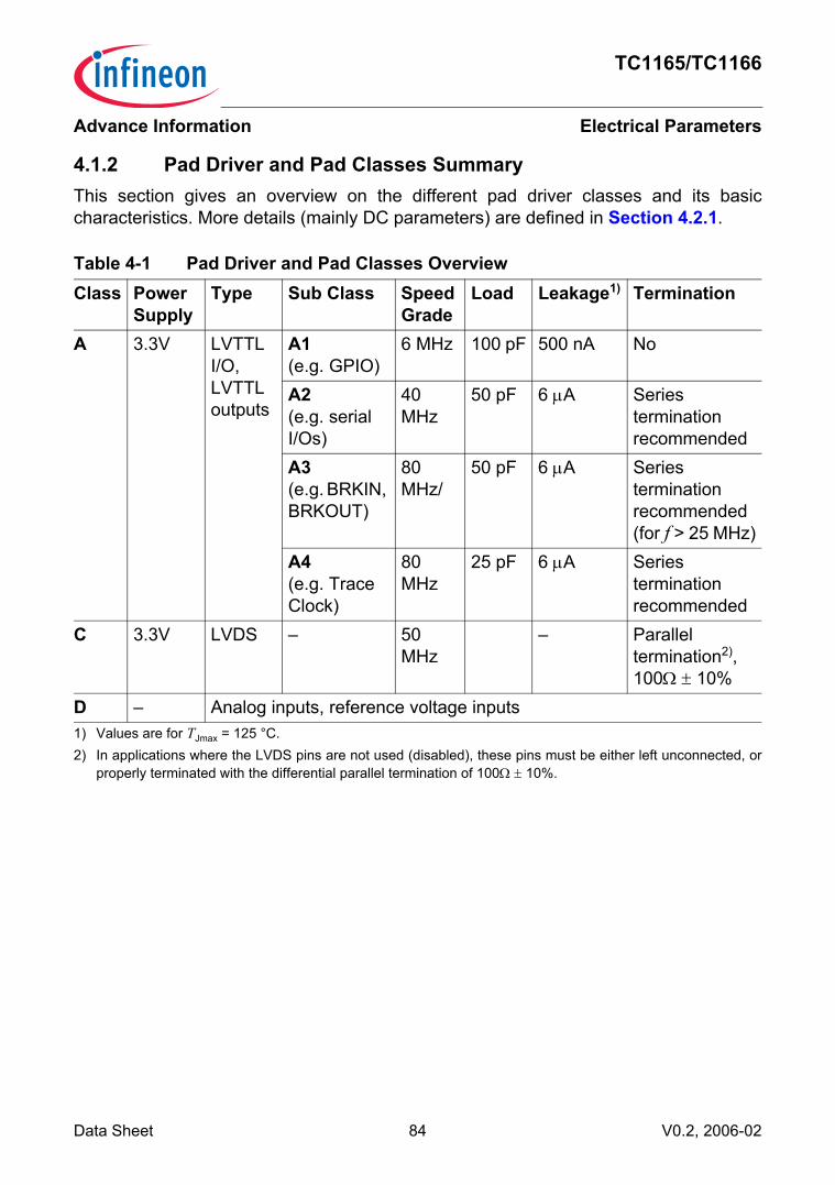
TC1165/TC1166
Electrical ParametersAdvance Information
4.1.2 Pad Driver and Pad Classes SummaryThis section gives an overview on the different pad driver classes and its basiccharacteristics. More details (mainly DC parameters) are defined in Section 4.2.1.
Table 4-1 Pad Driver and Pad Classes OverviewClass Power
SupplyType Sub Class Speed
GradeLoad Leakage1)
1) Values are for TJmax = 125 °C.
Termination
A 3.3V LVTTL I/O, LVTTL outputs
A1(e.g. GPIO)
6 MHz 100 pF 500 nA No
A2 (e.g. serial I/Os)
40 MHz
50 pF 6 µA Series termination recommended
A3(e.g. BRKIN, BRKOUT)
80 MHz/
50 pF 6 µA Series termination recommended(for f > 25 MHz)
A4(e.g. Trace Clock)
80 MHz
25 pF 6 µA Series termination recommended
C 3.3V LVDS – 50 MHz
– Parallel termination2), 100Ω ± 10%
2) In applications where the LVDS pins are not used (disabled), these pins must be either left unconnected, orproperly terminated with the differential parallel termination of 100Ω ± 10%.
D – Analog inputs, reference voltage inputs
Data Sheet 84 V0.2, 2006-02

TC1165/TC1166
Electrical ParametersAdvance Information
4.1.3 Absolute Maximum RatingsTable 4-2 shows the absolute maximum ratings of the TC1165/TC1166 parameters.
Note: Stresses above those listed under “Absolute Maximum Ratings” may causepermanent damage to the device. This is a stress rating only and functionaloperation of the device at these or any other conditions above those indicated inthe operational sections of this specification is not implied. Exposure to absolutemaximum rating conditions for extended periods may affect device reliability.During absolute maximum rating overload conditions (VIN > related VDD orVIN < VSS) the voltage on the related VDD pins with respect to ground (VSS) mustnot exceed the values defined by the absolute maximum ratings.
Table 4-2 Absolute Maximum Rating ParametersParameter Symbol Limit Values Unit Notes
Min. Max.Ambient temperature TA SR -40 85 °C Under biasStorage temperature TST SR -65 150 °C –Junction temperature TJ SR -40 125 °C Under biasVoltage at 1.5 V power supply pins with respect to VSS
1)
1) Applicable for VDD, VDDOSC, VDDPLL, and VDDAF.
VDD SR – 2.25 V –
Voltage at 3.3 V power supply pins with respect to VSS
2)
2) Applicable for VDDP, VDDFL3, VDDM, and VDDMF.
VDDP SR – 3.75 V –
Voltage on any Class A input pin and dedicated input pins with respect to VSS
VIN SR -0.5 VDDP + 0.5ormax. 3.7
V Whatever is lower
Voltage on any Class D analog input pin with respect to VAGND
VAIN,VAREFx
SR -0.5 VDDM + 0.5or max. 3.7
V Whatever is lower
Voltage on any Class D analog input pin with respect to VSSAF
VAINF,VFAREF
SR -0.5 VDDMF + 0.5or max. 3.7
V Whatever is lower
CPU & LMB Bus Frequency fCPU SR – 803)
3) The PLL jitter characteristics add to this value according to the application settings. See the PLL jitterparameters.
MHz –FPI Bus Frequency fSYS SR – 803) MHz 4)
4) The ratio between fCPU and fSYS is fixed at 1:1.
Data Sheet 85 V0.2, 2006-02

TC1165/TC1166
Electrical ParametersAdvance Information
4.1.4 Operating ConditionsThe following operating conditions must not be exceeded in order to ensure correctoperation of the TC1165/TC1166. All parameters specified in the following table refer tothese operating conditions, unless otherwise noted.
Table 4-3 Operating Condition ParametersParameter Symbol Limit
ValuesUnit Notes
ConditionsMin. Max.
Digital supply voltage1) VDDVDDOSC
SR 1.42 1.582) V –
VDDPVDDOSC3
SR 3.13 3.473) V For Class A pins(3.3V ± 5%)
VDDFL3 SR 3.13 3.473) V –Digital ground voltage VSS SR 0 V –Ambient temperature under bias
TA SR -40 +85 °C –
Analog supply voltages – – – – See separate specificationPage 4-92, Page 4-99
CPU clock fCPU SR –4) 805) MHz –Short circuit current ISC SR -5 +5 mA 6)
Absolute sum of short circuit currents of a pin group (see Table 4-4)
Σ|ISC| SR – 20 mA See note7)
Absolute sum of short circuit currents of the device
Σ|ISC| SR – 100 mA See note 7)
Inactive device pin current (VDD = VDDP = 0)
IID SR -1 1 mA –
External load capacitance CL SR – See DC characteristics
pF Depending on pin class
Data Sheet 86 V0.2, 2006-02

TC1165/TC1166
Electrical ParametersAdvance Information
1) Digital supply voltages applied to the TC1165/TC1166 must be static regulated voltages which allow a typicalvoltage swing of ±5%.
2) Voltage overshoot up to 1.7 V is permissible at Power-Up and PORST low, provided the pulse duration is lessthan 100 µs and the cumulated summary of the pulses does not exceed 1 h.
3) Voltage overshoot to 4 V is permissible at Power-Up and PORST low, provided the pulse duration is less than100 µs and the cumulated summary of the pulses does not exceed 1 h.
4) The TC1165/TC1166 uses a static design, so the minimum operation frequency is 0 MHz. Due to test timerestriction no lower frequency boundary is tested, however.
5) The PLL jitter characteristics add to this value according to the application settings. See the PLL jitterparameters.
6) Applicable for digital outputs.7) See additional document “TC1796 Pin Reliability in Overload“ for overload current definitions.
Data Sheet 87 V0.2, 2006-02

TC1165/TC1166
Electrical ParametersAdvance Information
Table 4-4 Pin Groups for Overload/Short-Circuit Current Sum ParameterGroup Pins1 TRCLK, P5.[7:0], P0.[7:6], P0.[15:14]2 P0.[13:12], P0.[5:4], P2.[13:8], SOP0A, SON0, FCLP0A, FCLN03 P0.[11:8], P0.[3:0], P3.[13:11]4 P3[10:0], P3.[15:14]5 HDRST, PORST, NMI, TESTMODE, BRKIN, BRKOUT, BYPASS, TCK,
TRST, TDO, TMS, TDI, P1.[7:4]6 P1.[3:0], P1.[11:8], P4.[3:0]7 P2.[7:0], P1.[14:12]8 P5.[15:8]
Data Sheet 88 V0.2, 2006-02

TC1165/TC1166
Electrical ParametersAdvance Information
4.2 DC ParametersThe electrical characteristics of the DC Parameters are detailed in this section.
4.2.1 Input/Output PinsTable 4-5 provides the characteristics of the input/output pins of the TC1165/TC1166.
Table 4-5 Input/Output DC-Characteristics (Operating Conditions apply)Parameter Symbol Limit Values Unit Test Conditions
Min. Max.General ParametersPull-up current1) |IPUH| CC 10 100 µA VIN < VIHAmin;
class A1/A2/Input pads.20 200 µA VIN < VIHAmin;
class A3/A4 pads.Pull-down current1)
|IPDL| CC 10 150 µA VIN > VILAmax; class A1/A2/Input pads.
20 200 µA VIN > VILAmax; class A3/A4 pads.
Pin capacitance1)
(Digital I/O)CIO CC – 10 pF f = 1 MHz
TA = 25 °CInput only Pads (VDDP = 3.13 to 3.47 V = 3.3V ±5%)Input low voltageclass A1/A2 pins
VILA SR -0.3 0.34 ×VDDP
V –
Input high voltageclass A1/A2 pins
VIHA SR 0.64 ×VDDP
VDDP+ 0.3 ormax. 3.6
V Whatever is lower
Ratio VIL/VIH CC 0.53 – – –Input low voltageclass A3 pins
VILA3 SR – 0.8 V –
Input high voltageclass A3 pins
VIHA3 SR 2.0 – V –
Input hysteresis HYSA CC 0.1 ×VDDP
– V 2)5)
Input leakage current
IOZI CC – ±3000
±6000
nA ((VDDP/2)-1) < VIN < ((VDDP/2)+1)otherwise3)
Data Sheet 89 V0.2, 2006-02

TC1165/TC1166
Electrical ParametersAdvance Information
Class A Pads (VDDP = 3.13 to 3.47 V = 3.3V ±5%)Output low voltage4)
VOLA CC – 0.4 V IOL = 2 mA for strong driver mode, (Not applicable to Class A1 pins)IOL = 1.8 mA for medium driver mode, A2 padsIOL = 1.4 mA for medium driver mode, A1 padsIOL = 370 µA for weak driver mode
Output high voltage3)
VOHA CC 2.4 – V IOH = -2 mA for strong driver mode, (Not applicable to Class A1 pins)IOH = -1.8 mA for medium driver mode, A1/A2 padsIOH = -370 µA for weak driver mode
VDDP - 0.4
– V IOH = -1.4 mA for strong driver mode, (Not applicable to Class A1 pins)IOH = -1 mA for medium driver mode, A1/A2 padsIOH = -280 µA for weak driver mode
Input low voltageclass A1/2 pins
VILA SR -0.3 0.34 ×VDDP
V –
Input high voltageclass A1/2 pins
VIHA SR 0.64 ×VDDP
VDDP + 0.3 or 3.6
V Whatever is lower
Ratio VIL/VIH CC 0.53 – – –Input hysteresis HYSA CC 0.1 ×
VDDP
– V 2)5)
Table 4-5 Input/Output DC-Characteristics (cont’d)(Operating Conditions Parameter Symbol Limit Values Unit Test Conditions
Min. Max.
Data Sheet 90 V0.2, 2006-02

TC1165/TC1166
Electrical ParametersAdvance Information
Input leakage current Class A2/3/4 pins
IOZA24 CC – ±3000
±6000
nA ((VDDP/2)-1) < VIN <((VDDP/2)+1)otherwise3)
Input leakage currentClass A1 pins
IOZA1 CC – ±500 nA 0 V <VIN < VDDP
Class C Pads (VDDP = 3.13 to 3.47 V = 3.3V ±5%)Output low voltage VOL CC 815 mV Parallel termination
100 Ω ± 1%Output high voltage
VOH CC 1545 mV
Output differential voltage
VOD CC 150 600 mV
Output offset voltage
VOS CC 1075 1325 mV
Output impedance R0 CC 40 140 –Class D Padssee ADC Characteristics – – – –1) Not subject to production test, verified by design / characterization.2) The pads that have spike filter function in the input path: PORST, HDRST, NMI do not have hysteresis.3) Only one of these parameters is tested, the other is verified by design characterization4) Max. resistance between pin and next power supply pin 25 Ω for strong driver mode
(verified by design characterization).5) Function verified by design, value is not subject to production test - verified by design/characterization.
Hysteresis is implemented to avoid metastable states and switching due to internal ground bounce. It cannotbe guaranteed that it suppresses switching due to external system noise.
Table 4-5 Input/Output DC-Characteristics (cont’d)(Operating Conditions Parameter Symbol Limit Values Unit Test Conditions
Min. Max.
Data Sheet 91 V0.2, 2006-02

TC1165/TC1166
Electrical ParametersAdvance Information
4.2.2 Analog to Digital Converter (ADC0)Table 4-6 provides the characteristics of the ADC module in the TC1165/TC1166.
Table 4-6 ADC Characteristics (Operating Conditions apply)
Parameter Symbol Limit Values Unit Test Conditions / RemarksMin. Typ. Max.
Analog supply voltage
VDDM SR 3.13 3.3 3.471) V –VDD SR 1.42 1.5 1.582) V Power supply for
ADC digital part, internal supply
Analog ground voltage
VSSM SR -0.1 – 0.1 V –
Analog reference voltage 17)
VAREFx SR VAGNDx+1V
VDDM VDDM+ 0.051)3)4)
V –
Analog reference ground 17)
VAGNDx SR VSSMx -0.05V
0 VAREF - 1 V
V –
Analog reference voltage range5)17)
VAREFx-VAGNDx
SR VDDM/2 VDDM + 0.05
Analog input voltage range
VAIN SR VAGNDx – VAREFx V –
VDDMsupply current
IDDM SR 2.5 4 mArms
6)
Power-up calibrationtime
tPUC CC – – 3840 fADC CLK
–
Internal ADC clocks
fBC CC 2 – 40 MHz fBC = fANA × 4fANA CC 0.5 – 10 MHz fANA = fBC / 4
Sample time tS CC 4 × (CHCONn.STC+ 2) × tBC
µs –
8 × tBC – – µs
Data Sheet 92 V0.2, 2006-02

TC1165/TC1166
Electrical ParametersAdvance Information
Conversion time tC CC tS + 40 × tBC + 2 × tDIV µs For 8-bit conversion
tS + 48 × tBC + 2 × tDIV µs For 10-bit conversion
tS + 56 × tBC + 2 × tDIV µs For 12-bit conversion
Total unadjusted error 5)
TUE7) CC – – ±1 LSB For 8-bit conv.– – ±2 LSB For 10-bit conv.– – ±4 LSB For 12-bit conv.8)9)
– – ±8 LSB For 12-bit conv.10)9)
DNL error11)5) TUEDNL CC – ±1.5 ±3.0 LSB For 12-bit conv.12) 9)
INL error11)5) TUEINL CC – ±1.5 ±3.0 LSB For 12-bit conv.12) 9)
Gain error11)5) TUEGAIN CC – ±0.5 ±3.5 LSB For 12-bit conv.12) 9)
Offset error11)5) TUEOFF CC – ±1.0 ±4.0 LSB For 12-bit conv.12) 9)
Input leakage current at analog inputs AN0, AN1 and AN31. see Figure 4-313)
IOZ114) CC –1000 – 300 nA (0% VDDM) < VIN <
(2% VDDM)–200 400 nA (2% VDDM) < VIN <
(95% VDDM)–200 1000 nA (95% VDDM) < VIN
< (98% VDDM)–200 3000 nA (98% VDDM) < VIN
< (100% VDDM)
Table 4-6 ADC Characteristics (cont’d) (Operating Conditions apply)
Parameter Symbol Limit Values Unit Test Conditions / RemarksMin. Typ. Max.
Data Sheet 93 V0.2, 2006-02

TC1165/TC1166
Electrical ParametersAdvance Information
Input leakage current at analog inputs AN2 to AN30, see Figure 4-3
IOZ114) CC –1000 – 200 nA (0% VDDM) < VIN <
(2% VDDM)–200 300 nA (2% VDDM) < VIN <
(95% VDDM)–200 1000 nA (95% VDDM) < VIN
< (98% VDDM)–200 3000 nA (98% VDDM) < VIN
< (100% VDDM)Input leakage current at VAREF
IOZ2 CC – – ±1 µA 0 V < VAREF <VDDM, no conversion running
Input current at VAREF
17)IAREF CC – 35 75 µA
rms0 V < VAREF <VDDM
15)
Total capacitance of the voltage reference inputs16)17)
CAREFTOT CC – – 25 pF 9)
Switched capacitance at the positive reference voltage input 17)
CAREFSW CC – 15 20 pF 9)18)
Resistance of the reference voltage input path16)
RAREF CC – 1 1.5 kΩ 500 Ohm increased for AN[1:0] used as reference input 9)
Total capacitance of the analog inputs16)
CAINTOT CC – – 25 pF 6)9)
Switched capacitance at the analog voltage inputs
CAINSW CC – – 7 pF 9)19)
Table 4-6 ADC Characteristics (cont’d) (Operating Conditions apply)
Parameter Symbol Limit Values Unit Test Conditions / RemarksMin. Typ. Max.
Data Sheet 94 V0.2, 2006-02

TC1165/TC1166
Electrical ParametersAdvance Information
ON resistance of the transmission gates in the analog voltage path
RAIN CC – 1 1.5 kΩ 9)
ON resistance for the ADC test (pull-down for AIN7)
RAIN7T CC 200 300 1000 Ω Test feature available only for AIN79)
Current through resistance for the ADC test (pull-down for AIN7)
IAIN7T CC – 15rms
30peak
mA Test feature available only for AIN79)
1) Voltage overshoot to 4 V are permissible, provided the pulse duration is less than 100 µs and the cumulatedsummary of the pulses does not exceed 1 h.
2) Voltage overshoot to 1.7 V are permissible, provided the pulse duration is less than 100 µs and the cumulatedsummary of the pulses does not exceed 1 h.
3) A running conversion may become inexact in case of violating the normal operating conditions (voltageovershoot).
4) If the reference voltage VAREF increases or the VDDM decreases, so that VAREF = ( VDDM + 0.05 V toVDDM + 0.07 V), then the accuracy of the ADC decreases by 4LSB12.
5) If a reduced reference voltage in a range of VDDM/2 to VDDM is used, then the ADC converter errors increase.If the reference voltage is reduced with the factor k (k<1), then TUE, DNL, INL Gain and Offset errors increasewith the factor 1/k.If a reduced reference voltage in a range of 1 V to VDDM/2 is used, then there are additional decrease in theADC speed and accuracy.
6) Current peaks of up to 6 mA with a duration of max. 2 ns may occur7) TUE is tested at VAREF = 3.3 V, VAGND = 0 V and VDDM = 3.3 V8) ADC module capability.9) Not subject to production test, verified by design / characterization.10) Value under typical application conditions due to integration (switching noise, etc.).11) The sum of DNL/INL/Gain/Offset errors does not exceed the related TUE total unadjusted error.12) For 10-bit conversions the DNL/INL/Gain/Offset error values must be multiplied with factor 0.25.
For 8-bit conversions the DNL/INL/Gain/Offset error values must be multiplied with 0.0625.13) The leakage current definition is a continuous function, as shown in Figure 4-3. The numerical values defined
determine the characteristic points of the given continuous linear approximation - they do not define stepfunction.
14) Only one of these parameters is tested, the other is verified by design characterization.
Table 4-6 ADC Characteristics (cont’d) (Operating Conditions apply)
Parameter Symbol Limit Values Unit Test Conditions / RemarksMin. Typ. Max.
Data Sheet 95 V0.2, 2006-02

TC1165/TC1166
Electrical ParametersAdvance Information
Figure 4-1 ADC0 Clock Circuit
15) IAREF_MAX is valid for the minimum specified conversion time. The current flowing during an ADC conversionwith a duration of up to tC = 25µs can be calculated with the formula IAREF_MAX = QCONV/tC. Every conversionneeds a total charge of QCONV = 150pC from VAREF. All ADC conversions with a duration longer than tC = 25µs consume an IAREF_MAX = 6µA.
16) For the definition of the parameters see also Figure 4-2.17) Applies to AIN0 and AIN1, when used as auxiliary reference inputs.18) This represents an equivalent switched capacitance. This capacitance is not switched to the reference voltage
at once. Instead of this smaller capacitances are successively switched to the reference voltage.19) The sampling capacity of the conversion C-Network is pre-charged to VAREF/2 before the sampling moment.
Because of the parasitic elements the voltage measured at AINx is lower then VAREF/2.
MCA04657_mod
ProgrammableClock Divider
(1:1) to (1:256)
fBCfDIVFractionalDivider
fCLC
fANA ProgrammableCounter
SampleTime tS
CON.CTC CHCONn.STC
fTIMER Control/Status LogicInterrupt Logic
External Trigger LogicExternal Multiplexer LogicRequest Generation Logic
A/D Converter Module
Arbiter(1:20)
Control Unit(Timer)
1:4
Data Sheet 96 V0.2, 2006-02
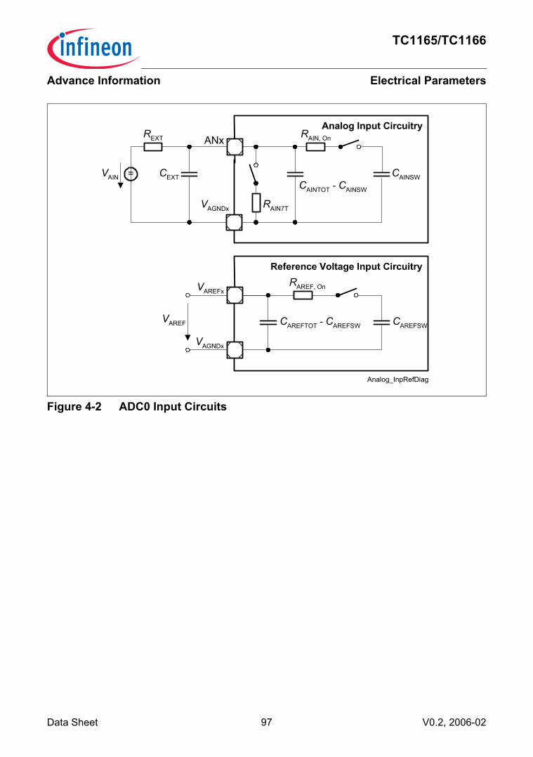
TC1165/TC1166
Electrical ParametersAdvance Information
Figure 4-2 ADC0 Input Circuits
Reference Voltage Input Circuitry
Analog Input Circuitry
Analog_InpRefDiag
REXT
=VAIN CEXT
RAIN, On
CAINTOT - CAINSW
CAINSW
ANx
VAREF
RAREF, On
CAREFTOT - CAREFSW CAREFSW
VAGNDx
VAREFx
RAIN7TVAGNDx
Data Sheet 97 V0.2, 2006-02

TC1165/TC1166
Electrical ParametersAdvance Information
Figure 4-3 ADC0 Analog Inputs Leakage
AN2 to AN30
VIN[VDDM%]300nA
1uA
3uA
2% 95% 100%98%
Ioz1
AN0, AN1 and AN31
VIN[VDDM%]400nA
-1uA
3uA
2% 95% 100%98%
Ioz1
300nA-200nA
200nA
1uA
-1uA
-200nA
Data Sheet 98 V0.2, 2006-02

TC1165/TC1166
Electrical ParametersAdvance Information
4.2.3 Fast Analog to Digital Converter (FADC)Table 4-7 provides the characteristics of the FADC module in the TC1165/TC1166.
Table 4-7 FADC Characteristics (Operating Conditions apply)Parameter Symbol Limit Values Unit Remarks
ConditionsMin. Max.DNL error EDNL CC – ±1 LSB 12)
INL error EINL CC – ±4 LSB 12)
Gradient error1)12) EGRAD CC – ±3 % 2)With calibration,gain 1, 2
– ±5 % Without calibrationgain 1, 2, 4
– ±6 % Without calibrationgain 8
Offset error12) EOFF3) CC – ±204) mV 2)With calibration
– ±604) mV Without calibrationReference error of internal VFAREF/2
EREF CC – ±60 mV –
Input leakage current at analog inputs AN32 to AN35.5) see Figure 4-5
IOZ16) CC –1000 300 nA (0% VDDM) < VIN <
(2% VDDM)–200 400 nA (2% VDDM) < VIN <
(95% VDDM)–200 1000 nA (95% VDDM) < VIN <
(98% VDDM)–200 3000 nA (98% VDDM) < VIN <
(100% VDDM)Analog supply voltages
VDDMF SR 3.13 3.477) V –VDDAF SR 1.42 1.588) V –
Analog ground voltage
VSSAF SR -0.1 0.1 V –
Analog reference voltage
VFAREF SR 3.13 3.477)9) V Nominal 3.3 V
Analog reference ground
VFAGND SR VSSAF -0.05V
VSSAF +0.05V
V –
Analog input voltage range
VAINF SR VFAGND VDDMF V –
Data Sheet 99 V0.2, 2006-02

TC1165/TC1166
Electrical ParametersAdvance Information
Analog supply currents
IDDMF SR – 9 mA –IDDAF SR – 17 mA 10)
Input current at each VFAREF
IFAREF CC – 150 µArms
Independent of conversion
Input leakage current at VFAREF
11)IFOZ2 CC – ±500 nA 0 V < VIN < VDDMF
Input leakage current at VFAGND
IFOZ3 CC ±8 µA
Conversion time tC CC – 21 CLK of fADC
For 10-bit conv.
Converter Clock fADC CC – 80 MHz –Input resistance of the analog voltage path (Rn, Rp)
RFAIN CC 100 200 kΩ 12)
Channel Amplifier Cutoff Frequency
fCOFF CC 2 MHz –
Settling Time of a Channel Amplifier after changing ENN or ENP
tSET CC 5 µsec –
1) Calibration of the gain is possible for the gain of 1 and 2, and not possible for the gain of 4 and 8.2) Callibration should be performed at each power-up. In case of continuous operation, callibration should be
performed minimum once per week.3) The offset error voltage drifts over the whole temperature range typically ±2 LSB.4) Applies when the gain of the channel equals one. For the other gain settings, the offset error increases; it must
be multiplied with the applied gain.5) The leakage current definition is a continuous function, as shown in Figure 4-5. The numerical values defined
determine the characteristic points of the given continuous linear approximation - they do not define stepfunction.
6) Only one of these parameters is tested, the other is verified by design characterization.7) Voltage overshoot to 4 V are permissible, provided the pulse duration is less than 100 µs and the cumulated
summary of the pulses does not exceed 1 h.8) Voltage overshoot to 1.7 V are permissible, provided the pulse duration is less than 100 µs and the cumulated
sum of the pulses does not exceed 1 h.9) A running conversion may become inexact in case of violating the normal operating conditions (voltage
overshoots).10) Current peaks of up to 40 mA with a duration of max. 2 ns may occur
Table 4-7 FADC Characteristics (cont’d)(Operating Conditions apply)Parameter Symbol Limit Values Unit Remarks
ConditionsMin. Max.
Data Sheet 100 V0.2, 2006-02

TC1165/TC1166
Electrical ParametersAdvance Information
The calibration procedure should run after each power-up, when all power supplyvoltages and the reference voltage have stabilized. The offset calibration must run first,followed by the gain calibration.
Figure 4-4 FADC Input Circuits
11) This value applies in power-down mode.12) Not subject to production test, verified by design / characterization.
FADC_InpRefDiag
=+
-
+
-
RNFAINxN
FAINxP
VFAGND
FADC Analog Input Stage
RP
VFAREF/2
VFAREF
FADC Reference VoltageInput Circuitry
VFAGND
VFAREF
IFAREF
Data Sheet 101 V0.2, 2006-02

TC1165/TC1166
Electrical ParametersAdvance Information
Figure 4-5 Analog Inputs AN32-AN35 Leakage
AN32 to AN35
VIN[VDDM%]400nA
-1uA
3uA
2% 95% 100%98%
Ioz1
300nA-200nA
1uA
Data Sheet 102 V0.2, 2006-02

TC1165/TC1166
Electrical ParametersAdvance Information
4.2.4 Oscillator PinsTable 4-8 provides the characteristics of the oscillator pins in the TC1165/TC1166.
Note: It is strongly recommended to measure the oscillation allowance (negativeresistance) in the final target system (layout) to determine the optimal parametersfor the oscillator operation. Please refer to the limits specified by the crystalsupplier.
Table 4-8 Oscillator Pins Characteristics (Operating Conditions apply)Parameter Symbol Limit values Unit Test Conditions
Min. Max.Frequency Range fOSC CC 4 25 MHz –Input low voltage at XTAL11)
1) If the XTAL1 pin is driven by a crystal, reaching a minimum amplitude (peak-to-peak) of 0.3 × VDDOSC3 isnecessary.
VILX SR -0.2 0.3 × VDDOSC3
V –
Input high voltage at XTAL11)
VIHX SR 0.7 × VDDOSC3
VDDOSC3+ 0.2
V –
Input current at XTAL1 IIX1 CC – ±25 µA 0 V < VIN < VDDOSC3
Data Sheet 103 V0.2, 2006-02

TC1165/TC1166
Electrical ParametersAdvance Information
4.2.5 Temperature SensorTable 4-9 provides the characteristics of the temperature sensor in the TC1165/TC1166.
Table 4-9 Temperature Sensor Characteristics (Operating Conditions apply)
Parameter Symbol Limit Values Unit RemarksMin. Max.
Temperature Sensor Range
TSR SR -40 150 °C –
Start-up time after resets inactive
tTSST SR 10 µs
Temperature of the die at the sensor location
TTS CC TTS = (ADC_Code - 487) × 0.396 - 40 °C 10-bit ADC result
TTS = (ADC_Code - 1948) × 0.099 - 40 °C 12Bit ADC result
Sensor Inaccuracy
TTSA CC ±10 °C
A/D Converter clock for DTS signal
fANA SR – 10 MHz Conversion with ADC0
Data Sheet 104 V0.2, 2006-02

TC1165/TC1166
Electrical ParametersAdvance Information
4.2.6 Power Supply CurrentTable 4-10 provides the characteristics of the power supply current in theTC1165/TC1166.
Table 4-10 Power Supply Current (Operating Conditions apply)
Parameter Symbol Limit Values Unit Test Conditions / Remarks
Min. Typ. Max.
PORST low current at VDD
IDD_PORST CC – – 63 mA The PLL running at the base frequency
PORST low current at VDDP
IDDP_PORST CC – – 5 mA The PLL running at the base frequency
Active mode core supply current1)
1) Infineon Power Loop: CPU running, all peripherals active. The power consumption of each custom applicationwill most probably be lower than this value, but must be evaluated separately.
IDD CC – – 260 mA fCPU = 80MHzfCPU/fSYS = 1:1
Active mode analog supply current
IDDAx;IDDMx
CC – – – mA See ADC0/FADC
Oscillator and PLL core power supply
IDDOSC CC – – 5 mA –
Oscillator and PLL pads power supply
IDDOSC3 CC – – 3.62)
2) Estimated value; double-bonded at package level with VDDP.
mA –
FLASH power supply current
IDDFL3 CC – – 45 mA –
LVDS port supply(via VDDP)3)
3) In case the LVDS pads are disabled, the power consumption per pair is negligible (less than 1mA).
ILVDS CC – – 25 mA LVDS pads active
Maximum Allowed Power Dissipation4)
4) For the calculation of the junction to ambient thermal resistance RTJA, see Chapter 5.1.
PDmax SR PD × RTJA < 40°C – At worst case, TA = 85 °C
Data Sheet 105 V0.2, 2006-02

TC1165/TC1166
Electrical ParametersAdvance Information
4.3 AC ParametersAll AC parameters are defined with the temperature compensation disabled, whichmeans that pads are constantly kept at the maximum strength.
4.3.1 Testing WaveformsThe testing waveforms for rise/fall time, output delay and output high impedance areshown in Figure 4-6, Figure 4-7 and Figure 4-8.
Figure 4-6 Rise/Fall Time Parameters
Figure 4-7 Testing Waveform, Output Delay
Figure 4-8 Testing Waveform, Output High Impedance
10%
90%
10%
90%
VSS
VDDP
tRrise_fall
tF
Mct04881_LL.vsd
VDDE / 2 Test Points VDDE / 2
VSS
VDDP
MCT04880_LL
VLoad + 0.1 V VOH - 0.1 VTimingReference
PointsVLoad - 0.1 V VOL - 0.1 V
Data Sheet 106 V0.2, 2006-02

TC1165/TC1166
Electrical ParametersAdvance Information
4.3.2 Output Rise/Fall TimesTable 4-11 provides the characteristics of the output rise/fall times in theTC1165/TC1166.
Table 4-11 Output Rise/Fall Times (Operating Conditions apply)
Parameter Symbol Limit Values Unit Test ConditionsMin. Max.
Class A1 PadsRise/fall times1)
Class A1 pads
1) Not all parameters are subject to production test, but verified by design/characterization and test correlation.
tRA1, tFA1 501401800015055065000
ns Regular (medium) driver, 50 pFRegular (medium) driver, 150 pFRegular (medium) driver, 20 nFWeak driver, 20 pFWeak driver, 150 pFWeak driver, 20 000 pF
Class A2 PadsRise/fall times 1)
Class A2 padstFA2, tFA2 3.3
65.516501401800015055065000
ns Strong driver, sharp edge, 50 pFStrong driver, sharp edge, 100pFStrong driver, med. edge, 50 pFStrong driver, soft edge, 50 pFMedium driver, 50 pFMedium driver, 150 pFMedium driver, 20 000 pFWeak driver, 20 pFWeak driver, 150 pFWeak driver, 20 000 pF
Class A3 PadsRise/fall times 1)
Class A3 padstFA3, tFA3 2.5 ns 50 pF
Class A4 PadsRise/fall times 1)
Class A4 padstFA4, tFA4 2.0 ns 25 pF
Class C PadsRise/fall times Class C pads
trC, tfC 2 ns
Data Sheet 107 V0.2, 2006-02

TC1165/TC1166
Electrical ParametersAdvance Information
4.3.3 Power SequencingThere is a restriction for the power sequencing of VDD and VDDP as shown in Figure 4-9:VDDP must always be higher than VDD - 0.5 V. The gray area shows the valid range forVDDP.
Figure 4-9 VDDP / VDD Power Up Sequence
All ground pins VSS must be externally connected to one single star point in the system.The difference voltage between the ground pins must not exceed 200 mV.The PORST signal must be activated at latest before any power supply voltage fallsbelow the levels shown on the figure below. In this case, only the memory row that wasthe target of the write at the moment of the power loss will contain unreliable content.Additionally, the PORST signal should be activated as soon as possible. The sooner thePORST signal is activated, the less time the system operates outside of the normaloperating power supply range.
PowerSeq
VDD(1.5V)
VDDP(3.3V)
VDD
VDDP
VDDP > VDD - 0.5VTime
Power Supply Voltage
Val
id a
rea
f or V
DD
P
Va li d area fo r V
DDP
Time
VDDP(3.3V)
PORST
Data Sheet 108 V0.2, 2006-02

TC1165/TC1166
Electrical ParametersAdvance Information
Figure 4-10 Power Down / Power Loss Sequence
VDDP
Power Supply Voltage
tPORST
VPORST3.3
VDDP-5%
-12%
3.3V3.13V
2.9VVDDPmin
t
tPORST
t
VDD-5%
-12%
1.5V1.42V
1.32V
VDD
VPORST1.5min
VDDmin
PowerDown3.3_1.5_reset_only_LL.vsd
Data Sheet 109 V0.2, 2006-02

TC1165/TC1166
Electrical ParametersAdvance Information
4.3.4 Power, Pad and Reset TimingTable 4-12 provides the characteristics of the power, pad and reset timing in theTC1165/TC1166.
Table 4-12 Power, Pad and Reset Timing ParametersParameter Symbol Limit Values Unit
Min. Max.Min. VDDP voltage to ensure defined pad states1)
1) This parameter is valid under assumption that PORST signal is constantly at low-level during the power-up/power-down of the VDDP.
VDDPPA CC 0.6 – V
Oscillator start-up time2)
2) This parameter is verified by device characterization. The external oscillator circuitry must be optimized by thecustomer and checked for negative resistance as recommended and specified by crystal suppliers.
tOSCS CC – 10 msMinimum PORST active time after power supplies are stable at operating levels
tPOA SR 10 – ms
HDRST pulse width tHD CC 1024 clock cycles3)
3) Any HDRST activation is internally prolonged to 1024 FPI bus clock (fSYS) cycles.
– fSYS
PORST rise time tPOR SR – 50 msSetup time to PORST rising edge4) tPOS SR 0 – nsHold time from PORST rising edge4) tPOH SR 100 – nsSetup time to HDRST rising edge5) tHDS SR 0 – nsHold time from HDRST rising edge5) tHDH SR 100 +
(2 × 1/fSYS)– ns
Ports inactive after PORST reset active6)7)
tPIP CC – 150 ns
Ports inactive after HDRST reset active8)
tPI CC – 150 +5 × 1/fSYS
ns
Minimum VDDP PORST activation threshold.9)
VPORST3.3 SR – 2.9 V
Minimum VDD PORST activation threshold. 9)
VPORST1.5 SR – 1.32 V
Power-on Reset Boot Time10) tBP CC 2.15 3.50 mSHardware/Software Reset Boot Time at fCPU=80MHz11)
tB CC 500 800 µS
Data Sheet 110 V0.2, 2006-02

TC1165/TC1166
Electrical ParametersAdvance Information
Figure 4-11 Power, Pad and Reset Timing
4) Applicable for input pins TESTMODE, TRST, BRKIN, and TXD1A with noise suppression filter of PORSTswitched-on (BYPASS = 0).
5) The setup/hold values are applicable for Port 0 and Port 4 input pins with noise suppression filter of HDRSTswitched-on (BYPASS = 0), independently whether HDRST is used as input or output.
6) Not subject to production test, verified by design / characterization.7) This parameter includes the delay of the analog spike filter in the PORST pad.8) Not subject to production test, verified by design / characterization.9) In case of power loss during internal flash write, prevents Flash write to random address.10) Booting from Flash, the duration of the boot-time is defined between the rising edge of the PORST and the
moment when the first user instruction has entered the CPU and its processing starts.11) Booting from Flash, the duration of the boot time is defined between the following events:
1. Hardware reset: the falling edge of a short HDRST pulse and the moment when the first user instruction hasentered the CPU and its processing starts, if the HDRST pulse is shorter than 1024 × TSYS. If the HDRST pulse is longer than 1024 × TSYS, only the time beyond the 1024 × TSYS should be added to theboot time (HDRST falling edge to first user instruction).2. Software reset: the moment of starting the software reset and the moment when the first user instructionhas entered the CPU and its processing starts
reset_beh
1) as program m ed
V D D P
P O R S T
H D R S T
P ads
P ad-sta te
undefined
tp i
V D D
V D D P PA V D D PP A
P ad-sta te
undefined
2) T ri-s ta te , pu ll dev ice ac tive
thd
V D D PR
O S C
toscs
1) 2) 1) 2)2)
tPO AtPO A
thd
Data Sheet 111 V0.2, 2006-02

TC1165/TC1166
Electrical ParametersAdvance Information
4.3.5 Phase Locked Loop (PLL)Section 4.3.5 provides the characteristics of the PLL parameters and its operation in theTC1165/TC1166.Note: All PLL characteristics defined on this and the next page are verified by design
characterization.
Phase Locked Loop OperationWhen PLL operation is enabled and configured, the PLL clock fVCO (and with it the CPUclock fCPU) is constantly adjusted to the selected frequency. The relation between fVCOand fSYS is defined by: fVCO = K × fCPU. The PLL causes a jitter of fCPU and affects theclock outputs TRCLK and SYSCLK (P4.3) which are derived from the PLL clock fVCO.There are two formulas that define the (absolute) approximate maximum value of jitterDP in ns dependent on the K-factor, the CPU clock frequency fCPU in MHz, and thenumber P of consecutive fCPU clock periods.
(4.1)
(4.2)
K : K-Divider ValueP : Number of fCPU periodsDP : Jitter in nsfCPU : CPU frequency in MHz
Table 4-13 PLL Parameters (Operating Conditions apply)Parameter Symbol Limit Values Unit
Min. Max.Accumulated jitter DP See Figure 4-12 –VCO frequency range fVCO 400 500 MHz
500 600 MHz600 700 MHz
PLL base frequency1)
1) The CPU base frequency which is selected after reset is calculated by dividing the limit values by 16 (this isthe K factor after reset).
fPLLBASE 140 320 MHz150 400 MHz200 480 MHz
PLL lock-in time tL – 200 µs
P K 900<× Dp ns[ ] 5 P×fcpu MHz[ ]----------------------------- 0 9,+
±=
P K 900≥× Dp ns[ ] 4500fcpu MHz[ ] K×---------------------------------------- 0 9,+
±=
Data Sheet 112 V0.2, 2006-02

TC1165/TC1166
Electrical ParametersAdvance Information
Note: The frequency of system clock fSYS can be selected to be either fCPU or fCPU/2.
With rising number P of clock cycles the maximum jitter increases linearly up to a valueof P that is defined by the K-factor of the PLL. Beyond this value of P the maximumaccumulated jitter remains at a constant value. Further, a lower CPU clock frequencyfCPU results in a higher absolute maximum jitter value.Figure 4-12 illustrates the jitter curve for several K/ fCPU combinations.
Figure 4-12 Approximated Maximum Accumulated PLL Jitter for Typical CPU Clock Frequencies fCPU (overview)
1±0.0
P [Periods]
±1.0
±2.0
±3.0
±5.0
25 50 75 100 125 150
±4.0
175
TC1165_TC1166_PLL_JITT
TC1165/TC1166 PLL Jitter (Preliminary)
±6.0
±7.0
±8.0
±9.0
±10.0
±11.0
±12.0
±13.0
Jitte
r [ns
]
fCPU = 80 MHz (K = 8)
fCPU = 80 MHz (K = 5)
fCPU = 66 MHz ( K = 7)
fCPU = 66 MHz (K = 10)
fCPU = 40 MHz
fCPU = 40 MHz (K = 10)
(K = 17)
oo
Data Sheet 113 V0.2, 2006-02

TC1165/TC1166
Electrical ParametersAdvance Information
Figure 4-13 Approximated Maximum Accumulated PLL Jitter for Typical CPU Clock Frequencies fCPU (detail)
Note: The maximum peak-to-peak noise on the main oscillator and PLL power supply(measured between VDDOSC and VSSOSC) is limited to a peak-to-peak voltage ofVPP = 10 mV. This condition can be achieved by appropriate blocking to the supplypins and using PCB supply and ground planes.
1±0.90
±1.00
±1.10
±1.40
2 3 4 5
TC1165_TC1166_PLL_DETAIL
TC1165_TC1166 PLL Jitter (preliminary )
±1.20
±1.30Jitte
r [ns
]
P [Periods]
fCPU = 40 MHz
fCPU = 66 MHz
fCP U = 80 MHz
Data Sheet 114 V0.2, 2006-02

TC1165/TC1166
Electrical ParametersAdvance Information
4.3.6 Debug Trace TimingVSS = 0 V; VDDP = 3.13 to 3.47 V (Class A); TA = -40 °C to +85 °C; CL (TRCLK) = 25 pF; CL (TR[15:0]) = 50 pF
Figure 4-14 Debug Trace Timing
Table 4-14 Debug Trace Timing Parameter1)
1) Not subject to production test, verified by design/characterization.
Parameter Symbol Limit Values UnitMin. Max.
TR[15:0] new state from TRCLK t9 CC -1 4 ns
T race_T m g
TR C LK
t9
TR [15:0 ] O ld S ta te N ew S ta te
Data Sheet 115 V0.2, 2006-02

TC1165/TC1166
Electrical ParametersAdvance Information
4.3.7 Timing for JTAG Signals(Operating Conditions apply, CL = 50 pF)
Figure 4-15 TCK Clock Timing
Table 4-15 TCK Clock Timing ParameterParameter Symbol Limit Values Unit
Min. Max.TCK clock period1)
1) fTCK should be lower or equal to fSYS
tTCK SR 25 – nsTCK high time t1 SR 10 – nsTCK low time t2 SR 10 – nsTCK clock rise time t3 SR – 4 nsTCK clock fall time t4 SR – 4 ns
TCK
t4
0.9 VDD
t3t1
0.1 VDD
t2tTCK
0.5 VDD
Data Sheet 116 V0.2, 2006-02

TC1165/TC1166
Electrical ParametersAdvance Information
Table 4-16 JTAG Timing Parameter1)
1) Not subject to production test, verified by design / characterization.
Parameter Symbol Limit Values
Unit Test Conditions / RemarksMin. Max.
TMS setup to TCK t1 SR 6.0 – ns –
TMS hold to TCK t2 SR 6.0 – ns –
TDI setup to TCK t1 SR 6.0 – ns –
TDI hold to TCK t2 SR 6.0 – ns –
TDO valid output from TCK2)
2) The falling edge on TCK is used to capture the TDO timing.
t3 CC – 14.5 ns CL = 50 pF3)4)
3) By reducing the load from 50 pF to 20 pF, a reduction of approximately 1.0 ns in timing is expected.4) By reducing the power supply range from +/-5 % to +5/-2 %, a reduction of approximately 0.5 ns in timing is
expected.
3.0 – CL = 20 pFTDO high impedance to valid output from TCK2)
t4 CC – 15.5 ns CL = 50 pF3)4)
TDO valid output to high impedance from TCK2)
t5 CC – 14.5 ns CL = 50 pF4)
Data Sheet 117 V0.2, 2006-02

TC1165/TC1166
Electrical ParametersAdvance Information
Figure 4-16 JTAG Timing
Note: The JTAG module is fully compliant with IEEE1149.1-2000 with JTAG clock at20 MHz. The JTAG clock at 40 MHz is possible with the modified timing diagramshown in Figure 4-16.
TMS
TDI
TCK
TDO
t1 t2
t1 t2
t4 t3 t5
Data Sheet 118 V0.2, 2006-02

TC1165/TC1166
Electrical ParametersAdvance Information
4.3.8 Peripheral TimingsSection 4.3.8 provides the characteristics of the peripheral timings in theTC1165/TC1166.Note: Peripheral timing parameters are not subject to production test. They are verified
by design/characterization.
4.3.8.1 Micro Link Interface (MLI) TimingTable 4-17 provides the characteristics of the MLI timing in the TC1165/TC1166.
Table 4-17 MLI Timing (Operating Conditions apply), CL = 50 pFParameter Symbol Limit Values Unit
Min. Max.TCLK/RCLK clock period1)2)
1) TCLK signal rise/fall times are the same as the A2 Pads rise/fall times.2) TCLK high and low times can be minimum 1 × TMLI
t30 CC/SR
2 × TMLI3)
3) TMLImin = TSYS = 1/fSYS. When fSYS = 80MHz, t30 = 25ns
– ns
MLI outputs delay from TCLK t35 CC 0 8 ns
MLI inputs setup to RCLK t36 SR 4 – ns
MLI inputs hold to RCLK t37 SR 4 – ns
RREADY output delay from RCLK t38 CC 0 8 ns
Data Sheet 119 V0.2, 2006-02

TC1165/TC1166
Electrical ParametersAdvance Information
Figure 4-17 MLI Interface TimingNote: The generation of RREADYx is in the input clock domain of the receiver. The
reception of TREADYx is asynchronous to TCLKx.
MLI_Tmg_1.vsd
TDATAxTVALIDx
t35 t35
t37t36
TCLKx0.1 VDDP
0.9 VDDP
RDATAxRVALIDx
RCLKx
t30
TREADYx
RREADYx
t38 t38
t30
Data Sheet 120 V0.2, 2006-02

TC1165/TC1166
Electrical ParametersAdvance Information
4.3.8.2 Micro Second Channel (MSC) Interface TimingTable 4-18 provides the characteristics of the MSC timing in the TC1165/TC1166.
Figure 4-18 MSC Interface Timing
Note: The data at SOP should be sampled with the falling edge of FCLP in the targetdevice.
Table 4-18 MSC Interface Timing (Operating Conditions apply), CL = 50 pFParameter Symbol Limit Values Unit
Min. Max.FCLP clock period1)2)
1) FCLP signal rise/fall times are the same as the A2 Pads rise/fall times.2) FCLP signal high and low can be minimum 1 × TMSC.
t40 CC 2 × TMSC3)
3) TMSCmin = TSYS = 1/fSYS. When fSYS = 80MHz, t40 = 25ns
– nsSOP/ENx outputs delay from FCLP t45 CC -10 10 ns
SDI bit time t46 SR 8 × TMSC – nsSDI rise time t48 SR 100 nsSDI fall time t49 SR 100 ns
MSC_Tmg_1.vsd
t45 t45
t40
0.1 VDDP
0.9 VDDP
t46
t48
0.1 VDDP
0.9 VDDP
t49
t46
SOPEN
FCLP
SDI
Data Sheet 121 V0.2, 2006-02

TC1165/TC1166
Electrical ParametersAdvance Information
4.3.8.3 Synchronous Serial Channel (SSC) Master Mode TimingTable 4-19 provides the characteristics of the SSC timing in the TC1165/TC1166.
Figure 4-19 SSC Master Mode Timing
Table 4-19 SSC Master Mode Timing (Operating Conditions apply), CL = 50 pFParameter Symbol Limit Values Unit
Min. Max.SCLK clock period1)2)
1) SCLK signal rise/fall times are the same as the A2 Pads rise/fall times.2) SCLK signal high and low times can be minimum 1 × TSSC.
t50 CC 2 × TSSC3)
3) TSSCmin = TSYS = 1/fSYS. When fSYS = 80 MHz, t50 = 25ns
– nsMTSR/SLSOx delay from SCLK t51 CC 0 8 ns
MRST setup to SCLK t52 SR 10 – ns
MRST hold from SCLK t53 SR 5 – ns
SSC_Tmg_1.vsd
SCLK1)2)
MTSR1)
t51 t51
MRST1)
t53
Datavalid
t52
SLSOx2)
t51
1) This timing is based on the following setup: CON.PH = CON.PO = 0.
2) The transition at SLSOx is based on the following setup: SSOTC.TRAIL = 0 and the first SCLK high pulse is in the first one of a transmission.
t50
Data Sheet 122 V0.2, 2006-02

TC1165/TC1166
Package and ReliabilityAdvance Information
5 Package and ReliabilityChapter 5 provides the information of the TC1165/TC1166 package and reliabilitysection..
5.1 Package Parameters (PG-LQFP-176-2)Table 5-1 provides the thermal characteristics of the package.
Table 5-1 Thermal Characteristics of the PackageParameter Symbol Limit Values Unit Notes
Min. Max.Thermal resistance junction case top1)
1) The top and bottom thermal resistances between the case and the ambient (RTCAT, RTCAB) are to be combinedwith the thermal resistances between the junction and the case given above (RTJCT, RTJCB), in order tocalculate the total thermal resistance between the junction and the ambient (RTJA). The thermal resistancesbetween the case and the ambient (RTCAT, RTCAB) depend on the external system (PCB, case) characteristics,and are under user responsibility.The junction temperature can be calculated using the following equation: TJ=TA+RTJA × PD, where the RTJA isthe total thermal resistance between the junction and the ambient. This total junction ambient resistance RTJAcan be obtained from the upper four partial thermal resistances, by a) simply adding only the two bottom thermal resistances (junction case bottom and case ambient bottom), or b) by taking all four resistances into account, depending on the precision needed.
RTJCT CC – 5.4 K/W –
Thermal resistance junction case bottom1)
RTJCB CC – 21.5 K/W –
Data Sheet 123 V0.2, 2006-02

TC1165/TC1166
Package and ReliabilityAdvance Information
5.2 Package OutlineFigure 5-1 shows the package outlines of the TC1165/TC1166.
Figure 5-1 Package Outlines PG-LQFP-176-2
PG-LQFP-176-2Plastic Low Profile Quad Flat Package
You can find all of our packages, sorts of packing and others in our Infineon Internet Page “Products”: http://www.infineon.com/products.
Dimensions in mmSMD = Surface Mounted Device
Data Sheet 124 V0.2, 2006-02

TC1165/TC1166
Package and ReliabilityAdvance Information
5.3 Flash Memory ParametersThe data retention time of the TC1165/TC1166’s Flash memory (i.e. the time after whichstored data can still be retrieved) depends on the number of times the Flash memory hasbeen erased and programmed.
Table 5-2 Flash ParametersParameter Symbol Limit Values Unit Notes
Min. Max.Program Flash Retention Time, Physical Sector1)2)
1) Storage and inactive time included.2) At average weighted junction temperature TJ = 100 °C.
tRET 15 – years Max. 1000 erase/program cycles
Program Flash Retention Time, Logical Sector1)2)
tRETL 15 – years Max. 100 erase/program cycles
Data Flash Endurance (128 Kbyte)
NE 15 000 – – Max. data retention time 2 years
Data Flash Endurance,EEPROM Emulation (8 × 16 Kbyte)
NE8 120 000 – – Max. data retention time 2 years
Programming Time per Page3)
3) In case the Program Verify feature detects weak bits, these bits will be programmed once more. Thereprogramming takes additional 5ms.
tPR – 5 ms –
Program Flash Erase Time per 256-Kbyte sector
tERP – 5 s fCPU = 80 MHz
Data Flash Erase Time per 16-Kbyte sector
tERD – 0.625 s fCPU = 80 MHz
Wake-up time tWU 4300 × 1/fCPU + 40µs
Data Sheet 125 V0.2, 2006-02

TC1165/TC1166
Package and ReliabilityAdvance Information
5.4 Quality DeclarationTable 5-3 shows the characteristics of the quality parameters in the TC1165/TC1166.
Note: Information about soldering can be found on the “package” information pageunder: http://www.infineon.com/products.
Table 5-3 Quality ParametersParameter Symbol Limit Values Unit Notes
Min. Max.ESD susceptibility according to Human Body Model (HBM)
VHBM – 2000 V Conforming to EIA/JESD22-A114-B
ESD susceptibility of the LVDS pins
VHBM1 – 500 V –
ESD susceptibility according to Charged Device Model (CDM) pins
VCDM – 500 V Conforming to JESD22-C101-C
Moisture Sensitivity Level (MSL)
VCDM – 3 V Conforming to J-STD-020C for 240°C
Data Sheet 126 V0.2, 2006-02
