taper structures for coupling into photonic crystal slab waveguides
TRANSCRIPT
Bienstman et al. Vol. 20, No. 9 /September 2003 /J. Opt. Soc. Am. B 1817
Taper structures for coupling into photonic crystalslab waveguides
Peter Bienstman
Ghent University, Interuniversity Micro-Electronics Centre, Sint-Pietersnieuwstraat 41, B-9000 Gent, Belgium
Solomon Assefa
Department of Electrical Engineering and Computer Science, Massachusetts Institute of Technology,Cambridge, Massachusetts 02139
Steven G. Johnson and John D. Joannopoulos
Department of Physics, Massachusetts Institute of Technology, Cambridge, Massachusetts 02139
Gale S. Petrich and Leslie A. Kolodziejski
Department of Electrical Engineering and Computer Science, Massachusetts Institute of Technology,Cambridge, Massachusetts 02139
Received January 8, 2003; revised manuscript received April 25, 2003
We present an adiabatic taper design in three dimensions for coupling light into photonic crystal defectwaveguides in a square lattice of circular dielectric rods. The taper is a two-stage structure in which the firststage makes the transition from a dielectric waveguide to a coupled-cavity waveguide. The second stage sub-sequently transforms the waveguide mode from an index-guided mode to a band-gap-guided mode. We dis-cuss differences between the two-dimensional device and its three-dimensional slab version. © 2003 OpticalSociety of America
OCIS codes: 060.1810, 130.3120, 230.7370.
1. INTRODUCTIONPhotonic crystals are very interesting candidates for therealization of photonic integrated circuits because of theirability to confine light, guide it around tight bends andperform a wealth of other optical functionality such as fil-tering and add–drop multiplexing.1–3
The ultimate confinement of light can be realized onlyin full three dimensional (3D) photonic crystals, whichare still very hard to fabricate. However, for short- tomedium-term applications, two-dimensional (2D) photo-nic crystal slabs offer an interesting alternative.4 Inthese structures, the horizontal confinement is providedby an in-plane, 2D, photonic crystal, while a slab wave-guide structure takes care of the vertical out-of-plane con-finement. Provided the index contrast is high enough,lossless guided modes can exist in these structures.
The practical use of these structures for photonic inte-grated circuits is limited if there are no good approachesto coupling light into them efficiently. It is the aim ofthis paper to present adiabatic coupling structures forphotonic crystal slab waveguides in the form of squarelattices of dielectric pillars in air. To the best of ourknowledge, coupling into these structures has never beenthoroughly investigated. There have been reports of cou-pling into 2D photonic crystal waveguides,5 but these didnot capture the out-of-plane aspect. Other papers didtake into account full three dimensionality, but dealt with
0740-3224/2003/091817-05$15.00 ©
crystal structures consisting of a triangular lattice of airholes in a dielectric.6,7 We want to focus here on the dualstructure of dielectric pillars in air because in these sys-tems, it is easier to achieve a monomode operating re-gime, and because scattering losses due to sidewall rough-ness might be lower. Moreover, rather than employingan ad hoc gradual transition, in this paper we exploit theexistence of an explicit adiabatic theorem for periodicsystems.8 Given the simple constraints imposed by thistheorem, we thus demonstrate the design of a 3D struc-ture that has an a priori guarantee of high transmissionfor a sufficiently gradual taper.
The rest of this paper is structured as follows. In Sec-tion 2 we describe the parameters of the waveguide struc-ture we use. The design of the coupling structure is thenstarted in Section 3 using a 2D model. Many of the is-sues involved in the taper design are already present intwo dimensions, which allows us to get a qualitative in-sight into the device physics using a model with lowercomputational demands. In Section 4 we draw on theseinsights to design a full 3D coupling structure. We showthat the 3D version of this structure is not a straightfor-ward application of the 2D design, but that additionalmodifications need to be made.
2. WAVEGUIDE STRUCTUREThe structure under study consists of a layer of GaAs(n 5 3.37) of thickness 830 nm over a 1500-nm alumi-
2003 Optical Society of America

1818 J. Opt. Soc. Am. B/Vol. 20, No. 9 /September 2003 Bienstman et al.
num oxide cladding layer (n 5 1.61). Below the oxidelayer is a GaAs substrate. This slab waveguide structureprovides vertical confinement in a high-index GaAs coresandwiched by low index air and oxide claddings. Byetching these layers, we create a lattice of circular dielec-tric rods with a lattice constant of a 5 500 nm. The rodradius is 0.30a. The etch depth (or height of the pillars)is 1430 nm, meaning that we etch 600 nm into the oxidelayer.
Fig. 1. Photonic crystal slab based on a square lattice of dielec-tric rods in air.
Fig. 2. Band diagram of defect modes in photonic crystal slabstructure of Fig. 1 for different defect radii.
Fig. 3. Experimental prototype of photonic crystal slab struc-ture.
A line-defect, TM-like waveguide is created by reducingthe rod radius of a row in the photonic crystal (Fig. 1).Figure 2 shows the band structure of such waveguides forvarying radii of the defect. Using a radius of 0.25a re-sults in a mode that is located in the center of the usablebandgap below the light line.
Figure 3 also shows a scanning-electron micrograph ofa preliminary structure consisting of a bulk crystal inGaAs with conventional input and output waveguides.
3. TWO-DIMENSIONAL COUPLINGANALYSISA. Untapered WaveguidesWe will first study a 2D version of this structure, not be-cause it will give quantitative results directly applicableto the 3D case, but because it will allow us to identifyqualitatively many of the issues in the coupler designearly at lower computational cost. In two dimensions thebandgap extends from 0.235 to 0.300 (in normalized fre-quency units c/a). If we choose a defect radius of 0.20a(instead of the r 5 0.25a used in three dimensions), wecreate a defect mode extending in frequency from thelower band edge to 0.270.
As input waveguide, we will consider a narrow-dielectric-ridge waveguide (photonic wire) with the samewidth as the defect diameter. Coupling from a broad-ridge waveguide to such a photonic wire is easily achievedby standard tapers and is not the focus of this paper.
Figure 4 shows the transmission through the unta-pered structure for a photonic crystal waveguide length of8 periods. These simulations were done with afrequency-domain model based on vectorial eigenmodeexpansion9 and a staircase approximation of the indexprofile with a resolution of 20 pixels per period. Thismodeling tool CAMFR is freely available from theInternet.10
Although there are frequencies for which the untaperedstructure achieves unity transmission, this phenomenonis entirely due to Fabry–Perot resonances, in which aparasitic cavity is formed by reflections from the inputand output facets. As a further illustration of this effect,we also plot in Fig. 4 transmission through a photoniccrystal waveguide with a different length (10 periods).The peaks are shifted because of the different cavitylength.
Figure 4 clearly shows that there is an imperfect con-version of the optical mode from the dielectric waveguideto the photonic crystal waveguide. One of the main rea-sons it is hard to achieve good coupling is the fundamen-tal difference in guiding mechanism and field profile be-tween these two waveguides.
In the dielectric waveguide, the waveguide mode con-sists entirely of forward-propagating field components.The waveguide mode in the photonic crystal is, of course,a forward-propagating Bloch mode, but because of thestrong scattering inside the crystal, this Bloch mode (withnet forward energy flux) consists of both forward- andbackward-propagating field contributions (Fourier compo-nents). Another way of looking at this is to note that theratio between the electric and magnetic field (related toan effective ‘‘impedance’’) will be very different for thesetwo waveguides.

Bienstman et al. Vol. 20, No. 9 /September 2003 /J. Opt. Soc. Am. B 1819
In the dielectric waveguide, the mode is guided by clas-sical total internal reflection in which the field is concen-trated in a region having a higher refractive index thanits surroundings. In the photonic crystal waveguide, theeffective index of the line defect is lower than that of itssurroundings because the radius of the defect rods issmaller than that of the bulk rods. In this case, the guid-ing mechanism is that light in the defect is channeled bytwo perfect mirrors formed by the adjacent bulk photoniccrystal.
Thus, to increase the coupling efficiency, we need to ad-dress these two issues. For that reason, we propose atwo-stage coupling structure in which stage I converts theforward dielectric mode into a mode with both forwardand backward components and stage II makes the transi-tion from high-effective-index guiding to low-effective-index guiding.
B. Stage I CouplerIn Fig. 5 we simulate a structure which makes an adia-batic transition from a dielectric waveguide to a (albeitrather strongly coupled) coupled-cavity waveguide alsocalled coupled-resonator optical waveguide)11 and thenback to a dielectric waveguide. In such a coupled reso-nator optical waveguide, the waveguide mode is, in fact, aBloch mode with both forward- and backward-
Fig. 4. Transmission through bulk crystal and two untaperedwaveguides of different lengths.
Fig. 5. Transmission through a stage I input coupler (geometryshown in the inset), a 20-period coupled-cavity waveguide (notshown in inset), and a stage I output coupler (mirror image of theinset).
propagating field components. By gradually decreasingthe distance between the resonators (in this particular ex-ample, by reducing the period by 10% each period), it isobvious that they will eventually merge to become a tra-ditional dielectric waveguide in which the mode has onlya forward-propagating field component.
As Fig. 5 shows, the transmission through such a struc-ture (both input and output coupler) can be practically100% over a large bandwidth. As an aside, we also wantto point out that not just any gradual geometric transitionwhich causes the rods to merge would give rise to 100%transmission. For example, keeping the period fixed andmaking the rods gradually more elliptical until theymerge would not give a high transmission, at least not inregions near the band edge of the coupled-cavity wave-guide. This is because the guided mode would leave thegap and no longer be guided, which is a necessary condi-tion for the adiabatic theorem for photonic crystals tohold.
Finally, we want to point out that the stage I structureis already useful in its own right (i.e., without the pres-
Fig. 6. Transmission through a ‘‘bad’’ taper structure in whichthe cladding rods are varied in diameter in stage II.
Fig. 7. Transmission through the two-stage input coupler, awaveguide of 8 or 10 periods length, and the output coupler.
1820 J. Opt. Soc. Am. B/Vol. 20, No. 9 /September 2003 Bienstman et al.
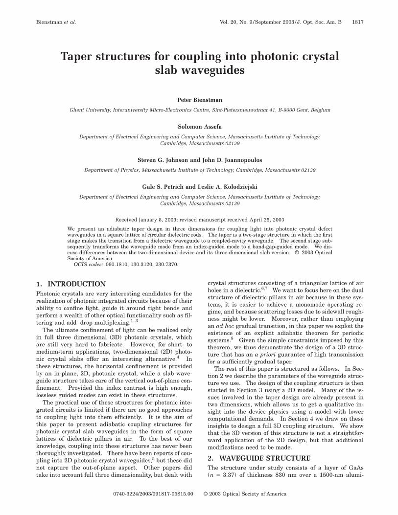
Fig. 8. Time snapshot of the electric field in the taper structure. Only the top half of the structure is shown.
ence of stage II), e.g., when coupling to coupled-cavitywaveguides.
C. Stage II CouplerWhen the adiabatic transition in stage I reaches the valueof the lattice constant, the input coupler can be seen as aphotonic crystal defect waveguide, but without the bulkphotonic crystal cladding. So the cladding needs to be in-troduced in stage II of the coupler, thereby transformingthe mode from high-index guiding to low-index guiding(gap guiding). One obvious approach to achieve this is tochange the cladding rod radius gradually from zero to itsfinal value (see Fig. 6). Such an approach was tried withreasonable success for crystal structures based on airholes in a dielectric6; however, there it was used in a dif-ferent context, namely to couple photonic crystalwaveguides of different widths. For coupling to the di-electric input waveguide, an abrupt transition was used,which yielded acceptable transmission because the wave-guide was rather wide (and therefore multimode, whichalso makes tapering more difficult).
In this paper, we want to achieve adiabatic tapering,not only to couple photonic crystal waveguides of differentwidths, but to make the transition from index guiding togap guiding. For this purpose, the gradual variation ofcladding radius does not work, as we can see in Fig. 6.The reason for this is that the taper goes through an in-termediate state (the box in the inset of Fig. 6) in whichthe core and cladding rods have the same diameter. Thissection is a bulk crystal which also has a band gap andtherefore reflects the incoming radiation. So, when de-signing a taper structure, one should ensure that each in-termediate stage has a guided mode and does not coupleto the radiative continuum.8 We should point out thatthis reflection and–or scattering from an intermediatestage is not due solely to some geometric coincidence, butis a fundamental issue which arises from the fact that by‘‘turning on’’ the bulk crystal, we pull the radiative con-tinuum down until it lies below the guided mode. So in-evitably there will always be an intermediate stage atwhich the waveguide mode crosses the continuum and isno longer guided.
The right way to achieve reflectionless adiabatic taper-ing is to keep the radius of the rods fixed, but to decreasegradually the distance between the cladding and the linedefect (see Fig. 7), in this case by 0.1a per period. In thisway, reflections do not occur from an intermediate stage
because the lower-band continuum always exists belowthe guided mode and only its local density of states isaltered.
As can be seen from Fig. 7, the transmission of the en-tire taper (stage I and stage II) is very close to 100% andhas a significant bandwidth. As in Fig. 4, we also plotthe transmission for two different waveguide lengths. Inthe range 0.245–0.255 the transmission does not varyfrom its near unity value, indicating very good modal con-version. For other frequencies, there are some shifts, butin general the transmission is much better than in the un-
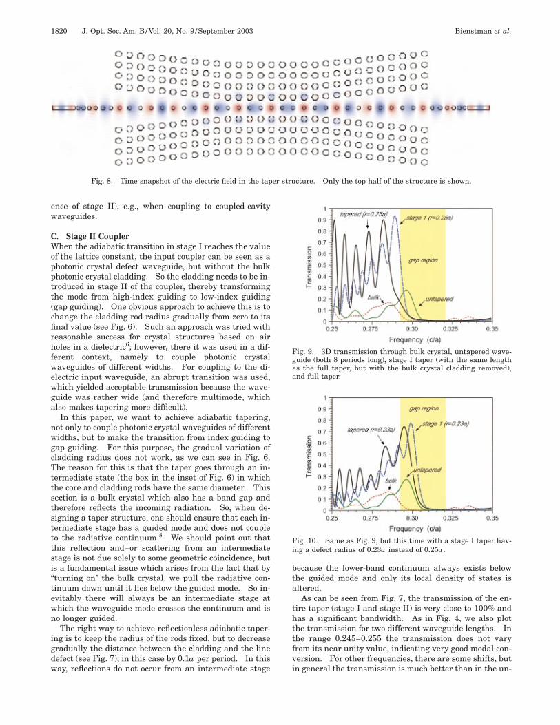
Fig. 9. 3D transmission through bulk crystal, untapered wave-guide (both 8 periods long), stage I taper (with the same lengthas the full taper, but with the bulk crystal cladding removed),and full taper.
Fig. 10. Same as Fig. 9, but this time with a stage I taper hav-ing a defect radius of 0.23a instead of 0.25a.

Bienstman et al. Vol. 20, No. 9 /September 2003 /J. Opt. Soc. Am. B 1821
tapered case. Once again, the adiabatic theorem guaran-tees that we can accomplish this transition arbitrarily bymaking the taper gradual enough.
In Fig. 8, we plot the field distribution in the entirestructure. It is obvious that there are differences in fieldprofiles in the dielectric waveguide, stage I, stage II, andthe photonic crystal waveguide. However, it is clear thatthe taper structure provides a gradual transition betweenthese profiles.
4. THREE-DIMENSIONAL COUPLINGANALYSISLet us now go back to the 3D case and the geometry de-scribed in Section 2. We use 3D finite-difference time-domain methods and a resolution of 20 pixels per periodto model the structures. Following the strategy of Sec-tion 3 to create a taper does not give rise to any transmis-sion inside the bandgap, as plotted in Fig. 9. This is be-cause the 3D defect mode has a much smaller bandwidthcompared with the 2D case. A similar observation is truefor stage I of the taper. The narrow pass bands of stage Iand the waveguide mode do not overlap in this case,which explains the lack of transmission inside the gap inFig. 9. This is remedied by slightly changing the rod ra-dius in stage I from 0.25a to 0.23a, which shifts the passband of stage I into the bandwidth of the waveguide mode(Fig. 10). In this case taper transmission is 75%, com-pared with 30% for the untapered case.
The adiabatic theorem guarantees that it should bepossible to achieve 100% transmission. However, for thisthe taper needs to be significantly more gradual than ourcomputational resources allow us to study. In the 3Dcase the group velocity is much lower and so is thek-vector phase mismatch with the reflected wave (becausewe operate near the edge of the Brillouin zone). Both fac-tors have a detrimental influence on the required taperlength.8
Additionally, because of resolution limitations, it is un-certain if 0.23a is really the optimal value for the stage Itaper radius, i.e., the one that gives the best alignmentbetween the two stages. This also means that fabricationtolerances will be rather stringent. Experimental verifi-cation is currently in progress.
5. CONCLUSIONSWe have presented novel two-stage taper designs whichallow efficient coupling from a dielectric waveguide to acoupled-cavity waveguide or to a line-defect waveguide ina photonic crystal slab of dielectric pillars in air. In two
dimensions these structures have nearly 100% transmis-sion and a very good bandwidth. For the design of the3D structures, special care needs to be taken to adjust theparameters of the two stages to have overlapping passbands. In three dimensions, despite the lower group ve-locities in the waveguide and the lower bandwidth of thetaper (0.005 c/a instead of 0.015 c/a as in two dimen-sions), the transmission can still be up to 75% with goodcontrol of the fabrication process.
6. ACKNOWLEDGMENTSP. Bienstman acknowledges support from the FlemishFund for Scientific Research (FWO-Vlaanderen) for apostdoctoral fellowship. Part of this work is supportedby the Materials Research Science and Engineering Cen-ter program of the National Science Foundation underaward DMB-9400334.
Corresponding author P. Bienstman may be reached bye-mail to [email protected].
REFERENCES1. E. Yablonovitch, ‘‘Photonic crystals,’’ J. Mod. Opt. 41, 173–
194 (1994).2. C. M. Soukoulis, ed., Photonic Bandgap Materials (Kluwer,
Dordrecht, The Netherlands, 1996).3. J. Joannopoulos, R. Meade, and J. Winn, Photonic Crystals:
Molding the Flow of Light (Princeton University, Princeton,N.J., 1995).
4. S. G. Johnson, P. R. Villeneuve, S. H. Fan, and J. D. Joan-nopoulos, ‘‘Linear waveguides in photonic-crystal slabs,’’Phys. Rev. B 62, 8212–8222 (2000).
5. A. Mekis and J. D. Joannopoulos, ‘‘Tapered couplers for ef-ficient interfacing between dielectric and photonic crystalwaveguides,’’ J. Lightwave Technol. 19, 861–865 (2001).
6. A. Talneau, P. Lalanne, M. Agio, and C. M. Soukoulis, ‘‘Low-reflection photonic-crystal taper for efficient coupling be-tween guide sections of arbitrary widths,’’ Opt. Lett. 27,1522–1524 (2002).
7. T. D. Happ, M. Kamp, and A. Forchel, ‘‘Photonic crystaltapers for ultracompact mode conversion,’’ Opt. Lett. 26,1102–1104 (2001).
8. S. G. Johnson, P. Bienstman, M. A. Skorobogatiy, M. Iba-nescu, E. Likoridis, and J. D. Joannopoulos, ‘‘The adiabatictheorem and a continuous coupled-mode theory for efficienttaper transitions in photonic crystals,’’ Phys. Rev. E 66,066608 (2002).
9. P. Bienstman and R. Baets, ‘‘Optical modelling of photoniccrystals and VCSELs using eigenmode expansion and per-fectly matched layers,’’ Opt. Quantum Electron. 33, 327–341 (2001).
10. http://camfr.sourceforge.net.11. Y. Xu, R. K. Lee, and A. Yariv, ‘‘Propagation and second-
harmonic generation of electromagnetic waves in a coupled-resonator optical waveguide,’’ J. Opt. Soc. Am. B 17, 387–400 (2000).