t8xc5121 -8-bit mcu with multi-protocol smart card … sheets/atmel pdfs...t89c5121 flash ram...
TRANSCRIPT

Rev. 4164G–SCR–07/06
8-bit Microcontroller with Multi-protocol Smart Card Interface
T83C5121T85C5121T89C5121AT83C5121AT85C5121AT89C5121
Features• 80C51 Core
– 12 or 6 Clocks per Instruction (X1 and X2 Modes)– 256 Bytes Scratchpad RAM– Dual Data Pointer– Two 16-bit Timer/Counters: T0 and T1
• T83C5121 with 16 Kbytes Mask ROM • T85C5121 with 16 Kbytes Code RAM• T89C5121 with 16 Kbytes Code RAM and 16 Kbytes EEPROM• On-chip Expanded RAM (XRAM): 256 Bytes• Versatile Host Serial Interface
– Full-duplex Enhanced UART (EUART) with Dedicated Baud Rate Generator (BRG): Most Standard Speeds up to 230K bits/s at 7.36 MHz
– Output Enable Input– Multiple Logic Level Shifters Options (1.8V to VCC)– Automatic Level Shifter Option
• Multi-protocol Smart Card Interface– Certified with Dedicated Firmware According to ISO 7816, EMV2000, GIE-CB, GSM
11.12V and WHQL Standards– Asynchronous Protocols T = 0 and T = 1 with Direct and Inverse Modes– Baud Rate Generator Supporting All ISO7816 Speeds up to D = 32/F = 372– Parity Error Detection and Indication– Automatic Character Repetition on Parity Errors – Programmable Timeout Detection– Card Clock Stop High or Low for Card Power-down Mode– Support Synchronous Card with C4 and C8 Programmable Outputs– Card Detection and Automatic De-activation Sequence– Step-up/down Converter with Programmable Voltage Output: 5V, 3V (± 8% at
60 mA) and 1.8V (±8% at 20 mA) – Direct Connection to Smart Card Terminals:
Short Circuit Current LimitationLogic Level Shifters 4 kV ESD Protection (MIL/STD 833 Class 3)
• Alternate Card Support with CLK, I/O and RST According to GSM 11.12V Standard• 2x I/O Ports: 6 I/O Port1 and 8 I/O Port3• 2x LED Outputs with Programmable Current Sources: 2, 4, or 10 mA• Hardware Watchdog• Reset Output Includes
– Hardware Watchdog Reset – Power-on Reset (POR)– Power-fail Detector (PFD)
• 4-level Priority Interrupt System with 7 Sources• 7.36 to 16 MHz On-chip Oscillator with Clock Prescaler• Absolute CPU Maximal Frequency: 16 MHz in X1 mode, 8MHz in X2 mode• Idle and Power-down Modes • Voltage Operation: 2.85V to 5.4V• Low Power Consumption
– 8 mA Operating Current (at 5.4V and 3.68 MHz)– 150 mA Maximum Current with Smart Card Power-on (at 16 MHz X1 Mode)– 30 μA Maximum Power-down Current at 3.0V (without Smart Card)– 100 μA Maximum Power-down Current at 5.4V (without Smart Card)
• Temperature Range– Commercial: 0 to +70°C Operating Temperature– Industrial: -40 to +85°C Operating Temperature
• Packages – SSOP24– QFN32– PLCC52

Description T8xC5121 is a high performance CMOS ROM/CRAM derivative of the 80C51 CMOSsingle chip 8-bit microcontrollers.
T8xC5121 retains the features of the Atmel 80C51 with extended ROM capacity (16Kbytes), 512 bytes of internal RAM, a 4-level interrupt system, two 16-bit timer/counters(T0/T1), a full duplex enhanced UART (EUART) with baud rate generator (BRG) and anon-chip oscillator.
In addition, the T8xC5121 have, a Multi protocol Smart Card Interface, a dual datapointer, 2 programmable LED current sources (2-4-10 mA) and a hardware Watchdog.
T89C5121 Flash RAM version and T85C5121 Code RAM version can be loaded by In-System Programming (ISP) software residing in the on-chip ROM from a low-cost exter-nal serial EEPROM or from R232 interface.
T8xC5121 have 2 software-selectable modes of reduced activity for further reduction inpower consumption.
Block Diagram
Figure 1. Block Diagram
Notes: 1. Alternate function of Port 12. Alternate function of Port 33. Only for the Code RAM version4. Only for PLCC52
Timer 0 INT
RAM256 x8
T0 T1
RxD
TxD
XTAL2
XTAL1
EUART
CPU
Timer 1
INT
1
Ctrl
INT
0
C51 CORE
(2) (2) (2) (2)
P1
IB-bus
RS
T
VS
SV
CC
(1):
ROMXtalOsc
XRAM256x8
SCIB
CC8
CRST
CPRES
CIO
CC4
CCLK
CVCC
6 I/Os
LI
CRST1
CIO1
CCLK1
(2)
(2)
(2)(4)
16K x8CRAM16K x8
(2) (2)
P3
8 I/Os
DV
CC
VoltageReg.
(1)(1)(1)(1)(1)(1)
LEDDriveDirect
LED
0
LED
1
(2)(2)
Output
:1-16Clock
(3)
Prescaler
X2
Watchdog
EV
CC
CV
SS
P2
P0
EAPSEN
ALE
DC/DCConverter
Level Shifters
PORPFD
AlternateCard
BRG
Parallel I/O Ports
2 A/T8xC51214164G–SCR–07/06

A/T8xC5121
Pin Description Figure 2. 24-pin SSOP Pinout
Figure 3. QFN32 Pinout
P1.1/CC8
P1.4/CCLK
P1.0/CIORST
P1.5/CRST
1
P1.3/CC4
P1.2/CPRES
XTAL1
P3.3/INT1/OE
P3.2/INT0
P3.4/T0
P3.5/CIO1/T1
LICVCC
CVSS VCCEVCC
VSS P3.0/RxD
P3.1/TxD
2
3 4
5
6
78
9
10
1112
24
2322
21
20
19
18
17
16
15
14
13
P3.6/CCLK1/LED0XTAL2
P3.7/CRST1/LED1
DVCC
N/C
QFN32
Vss
P1.1/CC8
P1.0/CIO
P1.2/CPRES
CVcc
P1.4/CCLK
P3
.6/C
CLK
1/LE
D0
N/C
XTA
L1
P3.
7/C
RS
T1
/LE
D1
N/C
XTA
L2
P3.5/CIO1/T1
P1.3/CC4
P1.5/CRST
Vcc
CV
ss
EV
cc
N/C
DV
ccP3.4/T0
P3.0/RxD
28 27 261234567
24232221201918
1211109 13 14 15RST 8
1617
Vss
P3.1/TxD
LI
N/C
2529303132
N/C
P3.2/INT0
P3.3/INT1/OE
N/C
34164G–SCR–07/06
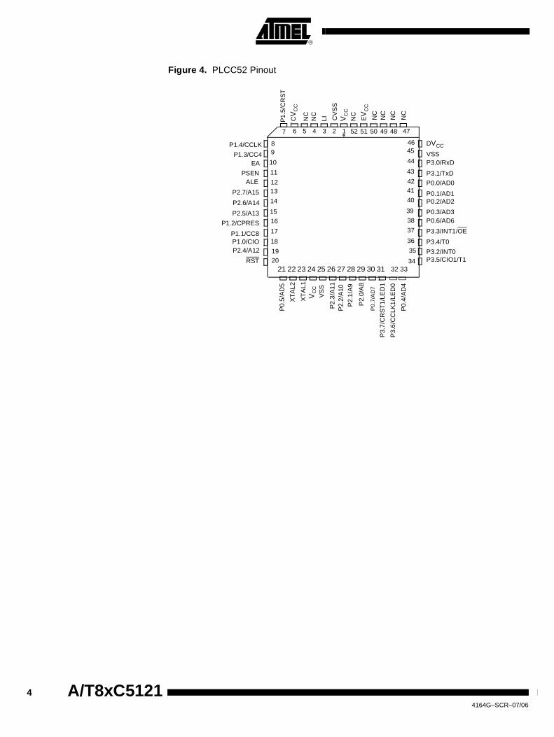
Figure 4. PLCC52 Pinout
21 22 26252423 292827 30 31
5 4 3 2 1 6 52 51 50 49 48
LICV
CC
VSS
DVCC
P0.1/AD1
P0.0/AD0
P0.2/AD2
P0.
5/A
D5
P0.6/AD6P0.3/AD3
P0.
4/A
D4
P0
.7/A
D7
P3.
6/C
CLK
1/L
ED
0
P3.
7/C
RS
T1/
LED
1
XT
AL1
P2.7/A15
P2.6/A14
P2.5/A13
P2.4/A12
P2.
2/A
10
P2.
1/A
9
P2.
0/A
8
P3.0/RxD
P3.1/TxD
P1.
5/C
RS
T
P1.4/CCLK
P1.3/CC4
P1.2/CPRES
P1.1/CC8P1.0/CIO
EA
PSENALE
P2.
3/A
11
89
10
11
1213
14
15
16
17
18
4645
44
43
4241
40
39
38
37
36
7 47
19 20
32 33 34
35 P3.2/INT0
P3.3/INT1/OE
RST
XT
AL
2
P3.5/CIO1/T1
P3.4/T0
VC
C
CV
SS
VC
C
VS
S
NC
NC
NC
EV
CC
NC
NC
NC
NC
4 A/T8xC51214164G–SCR–07/06

A/T8xC5121
Signals All the T8xC5121 signals are detailed in Table 1.
The port structure is described in Section “Port Structure Description”.
Table 1. Ports Description
PortSignal Name Alternate
Internal
Power
Supply ESD Type Description
P1.0 CIO CVCC 4 kV I/OSmart card interface function
Card I/O.
I/OInput/Output function
P1.0 is a bi-directional I/O port .
IReset configuration
Input .
P1.1 CC8 CVCC 4 kV OSmart card interface function
Card contact 8
OOutput function
P1.1 is a Push-pull port.
IReset configuration
Input
P1.2 CPRES VCC 4 kV ISmart card interface function
Card presence
I/OInput/Output function
P1.2 is a bi-directional I/O port with internal pull-ups- ( External Pull-up configuration can be selected).
IReset configuration
Input (high level due to internal pull-up)
P1.3 CC4 CVCC 4 kV OSmart card interface function
Card contact 4
OOutput function
P1.3 is a Push-pull port.
IReset configuration
Input (high level due to internal pull-up)
P1.4 CCLK CVCC 4 kV OSmart card interface function
Card clock
I/OInput/Output function
P1.4 is a a Push-pull port.
OReset configuration
Output at low level
P1.5 CRST CVCC 4 kV OSmart card interface function
Card reset
I/OInput/Output function
P1.5 is a a Push-pull port.
OReset configuration
Output at low level
54164G–SCR–07/06
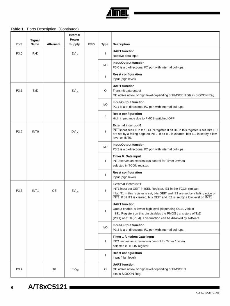
P3.0 RxD EVCC IUART function
Receive data input
I/OInput/Output function
P3.0 is a bi-directional I/O port with internal pull-ups.
IReset configuration
Input (high level)
P3.1 TxD EVCC O
UART function
Transmit data output
OE active at low or high level depending of PMSOEN bits in SIOCON Reg.
I/OInput/Output function
P3.1 is a bi-directional I/O port with internal pull-ups.
ZReset configuration
High impedance due to PMOS switched OFF
P3.2 INT0 DVCC I
External interrupt 0
INT0 input set IE0 in the TCON register. If bit IT0 in this register is set, bits IE0 are set by a falling edge on INT0. If bit IT0 is cleared, bits IE0 is set by a low level on INT0.
I/OInput/Output function
P3.2 is a bi-directional I/O port with internal pull-ups.
I
Timer 0: Gate input
INT0 serves as external run control for Timer 0 when
selected in TCON register.
IReset configuration
Input (high level)
P3.3 INT1 OE EVCC I
External Interrupt 1
INT1 input set OEIT in ISEL Register, IE1 in the TCON register.
If bit IT1 in this register is set, bits OEIT and IE1 are set by a falling edge on INT1. If bit IT1 is cleared, bits OEIT and IE1 is set by a low level on INT1
I
UART function
Output enable. A low or high level (depending OELEV bit in
ISEL Register) on this pin disables the PMOS transistors of TxD
(P3.1) and T0 (P3.4). This function can be disabled by software
I/OInput/Output function
P3.3 is a bi-directional I/O port with internal pull-ups.
I
Timer 1 function: Gate input
INT1 serves as external run control for Timer 1 when
selected in TCON register.
IReset configuration
Input (high level)
P3.4 T0 EVCC O
UART function
OE active at low or high level depending of PMSOEN
bits in SIOCON Reg.
Table 1. Ports Description (Continued)
PortSignal Name Alternate
Internal
Power
Supply ESD Type Description
6 A/T8xC51214164G–SCR–07/06

A/T8xC5121
I/OInput/Output function
P3.4 is a bi-directional I/O port with internal pull-ups.
I
Timer 0 function: External clock input
When Timer 0 operates as a counter, a falling edge on the T0 pin
increments the count.
ZReset configuration
High impedance due to PMOS switched OFF
P3.5 CIO1 DVCC I/OAlternate card function
Card I/O
I/OInput/Output function
P3.5 is a bi-directional I/O port with internal pull-ups.
I
Timer 1 function: External clock input
When Timer 1 operates as a counter, a falling edge on the T1 pin
increments the count.
IReset configuration
Input (high level due to internal pull-up)
P3.6 CCLK1 LED0 DVCC OAlternate card function
Card clock
O
LED function
These pins can be directly connected to the cathode of standard
LED without external current limiting resistors. The typical current
of each output can be programmed by software to 2, 4 or 10 mA
(LEDCON register).
I/OInput/Output function
P3.6 is a LED port.
IReset configuration
Input at high level
P3.7 CRST1 DVCC OAlternate card function
Card reset
P3.7 CRST1 LED1 DVCC O LED function
These pins can be directly connected to the cathode of standard
LED without external current limiting resistors. The typical current
of each output can be programmed by software to 2, 4 or 10 mA
(LEDCON register).
I/O Input/Output function
P3.7 is a a LED port.
I Reset configuration
Input at high level
Table 1. Ports Description (Continued)
PortSignal Name Alternate
Internal
Power
Supply ESD Type Description
74164G–SCR–07/06

RST VCC I/O Reset input
Holding this pin low for 64 oscillator periods while the oscillator
is running resets the device. The Port pins are driven to their reset
conditions when a voltage lower than VIL is applied, whether or
not the oscillator is running.
This pin has an internal pull-up resistor which allows the device to be reset by
connecting a capacitor between this pin and VSS.This capacitor is optional
thanks to the internal POR which output a Reset as long as Vcc has not
reached the POR threshold level
Asserting RST when the chip is in Idle mode or Power-down mode
returns the chip to normal operation.
The output is active for at least 12 oscillator periods when an internal
reset occurs.
XTAL1 VCC I Input to the on-chip inverting oscillator amplifier
To use the internal oscillator, a crystal/resonator circuit is connected
to this pin.
If an external oscillator is used, its output is connected to this pin.
XTAL2 VCC O Output of the on-chip inverting oscillator amplifier
To use the internal oscillator, a crystal/resonator circuit is connected
to this pin.
If an external oscillator is used, XTAL2 may be left unconnected.
VCC PWR Supply voltage
VCC is used to power the internal voltage regulators and internal I/O’s.
LI PWR DC/DC input
LI must be tied to VCC through an external coil (typically 4, 7 μH) and provide the current for the pump charge of the DC/DC converter.
CVCC PWR Card Supply voltage
CVCC is the programmable voltage output for the Card interface.
It must be connected to an external decoupling capacitor.
DVCC PWR Digital Supply voltage
DVCC is used to supply the digital core and internal I/Os. It is
internally connected to the output of a 3V regulator and must be connected to an external decoupling capacitor.
EVCC VCC PWR Extra supply voltage
EVCC is used to supply the level shifters of UART interface I/O
pins. It must be connected to an external decoupling capacitor.
This reference voltage is generated internally (automatically or not),
or it can be connected to an external voltage reference.
CVSS GND DC/DC ground
CVSS is used to sink high shunt currents from the external coil.
VSS GND Ground
Table 1. Ports Description (Continued)
PortSignal Name Alternate
Internal
Power
Supply ESD Type Description
8 A/T8xC51214164G–SCR–07/06

A/T8xC5121
ONLY FOR PLCC52 version
P0[7:0] AD[7:0] VCC I/O Input/Output function Port 0
P0 is an 8-bit open-drain bi-directional I/O port. Port 0 pins that
have 1s written to them float and can be used as high impedance
inputs. To avoid any parasitic current consumption, Floating P0
inputs must be pulled to VCC or VSS.
I/O Address/Data low
Mutiplexed Address/Data LSB for external access
P2[7:0] A[15:8] VCC I/O Input/Output function Port 2
P2 is an 8-bit open-drain bi-directional I/O port with internal pull-ups
O Address high
Address Bus MSB for external access
P3.6 WR DVCC O Write signal
Write signal asserted during external data memory write operation
P3.7 RD DVCC I Read signal
Read signal asserted during external data memory read operation
ALE VCC O Address latch enable output
The falling edge of ALE strobes the address into external latch
PSEN PSEN VCC O Program strobe enable
EA EA VCC I External access enable
This pin must be held low to force the device to fetch code from
external program memory starting at address 0000h. It is latched
during reset and cannot be dynamically changed during operation.
Table 1. Ports Description (Continued)
PortSignal Name Alternate
Internal
Power
Supply ESD Type Description
94164G–SCR–07/06

Port Structure Description
The different ports structures are described as follows.
Quasi Bi-directional Output Configuration
The default port output configuration for standard I/O ports is the quasi bi-directional out-put that is common on the 80C51 and most of its derivatives. This output type can beused as both an input and output without the need to reconfigure the port. This is possi-ble because when the port outputs a logic high, it is weakly driven, allowing an externaldevice to pull the pin low. When the port outputs a logic low state, it is driven stronglyand able to sink a fairly large current. These features are somewhat similar to an opendrain output except that there are three pull-up transistors in the quasi bi-directional out-put that serve different purposes. One of these pull-ups, called the weak pull-up, isturned on whenever the port latch for the pin contains a logic 1. The weak pull-upsources a very small current that will pull the pin high if it is left floating. A second pull-up, called the medium pull-up, is turned on when the port latch for the pin contains alogic 1 and the pin itself is also at a logic 1 level. This pull-up provides the primarysource current for a quasi bi-directional pin that is outputting a 1. If a pin that has a logic1 on it is pulled low by an external device, the medium pull-up turns off, and only theweak pull-up remains on. In order to pull the pin low under these conditions, the externaldevice has to sink enough current to overpower the medium pull-up and take the voltageon the port pin below its input threshold.
Figure 5. Quasi Bi-directional Output Configuration
Push-pull Output Configuration
The Push-pull output configuration has the same pull-down structure as the quasi bi-directional output modes, but provides a continuous strong pull-up when the port latchcontains a logic 1. The Push-pull mode may be used when more source current isneeded from a port output. The Push-pull port configuration is shown in Figure 5.
2 CPU
Input
Pin
Strong Weak Medium
N
P PP
CLOCK DELAY
Port latch
Data
Data
PMOS
NMOS
10 A/T8xC51214164G–SCR–07/06

A/T8xC5121
Figure 6. Push-pull Output Configuration
LED Output Configuration The input only configuration is shown in Figure 7.
Figure 7. LED Source Current Configuration
Note: The port can be configured in quasi bi-directional mode and the level of current can be programmed by means of LEDCON0and LEDCON1 registers before switching the led on by writing a logical 0 in Port latch.
Input
Pin
Strong
N
P
Port latch
Data
Data
PMOS
NMOS
Pin
Port LatchData
InputData
LEDx.0
LEDx.1
P
N
N
N
Weak2 CPU
P
CLOCK DELAYPMOS Strong Medium
P
NMOS
LED1CTRL
LED2CTRL
114164G–SCR–07/06
SFR Mapping The Special Function Registers (SFR) of the T8xC5121 belongs to the followingcategories:
• C51 core registers: ACC, B, DPH, DPL, PSW, SP
• I/O port registers: P0, P1, P2, P3
• Timer 0 registers: TCON, TH0, TH1, TMOD, TL0, TL1
• Serial I/O port registers: SADDR, SADEN, SBUF, SCON, BRL, BDRCON
• Power and clock control registers: PCON, CKRL, CKCON0, CKCON1, DCCKPS
• Interrupt system registers: IE0, IPL0, IPH0, IE1,IPL1, IPH1, ISEL
• Watchdog Timer 0: WDTRST, WDTPRG
• Others: AUXR, AUXR1, RCON
• Smart Card Interface: SCSR, SCCON/SCETU0, SCISR/SCETU1, SCIER/SCIIR, SCTBUF/SCRBUF, SCGT0/SCWT0, SCGT1/SCWT1, SCICR/SCWT2
• Port configuration: SIOCON, LEDCON
12 A/T8xC51214164G–SCR–07/06

A/T8xC5121
Reserved
Table 2. SFR Addresses and Reset Values
0/8 1/9 2/A 3/B 4/C 5/D 6/E 7/F
F8h FFh
F0h B0000 0000
LEDCONXXXX 0000
F7h
E8h EFh
E0h ACC0000 0000
E7h
D8h DFh
D0h PSW0000 0000
RCONXXXX OXXX
D7h
C8h CFh
C0h C7h
B8h IPL0XXX0 0000
SADEN0000 0000
ISEL0000 0100
DCCKPSXXXX XX11
BFh
B0hP3
1111 1111IE1
XXXX 0XXXIPL1
XXXX 0XXXIPH1
XXXX 0XXX
0 SCWT0 *1000 0000
0 SCWT1 *0010 0101
0 SCWT2 *0000 0000 IPH0
XXX0 0000
B7h
1 SCGT0 * 0000 1100
1 SCGT1* 0000 0000
1 SCICR *0000 0000
A8hIE0
0XX0 0000SADDR
0000 0000
SCTBUF*0000 0000 SCSR
XXX0 1000
0 SCCON * 0X000
0 SCISR*10X0 0000
0 SCIIR* 0X00 0000 CKCON1
XXXX 0XXX
AFh
SCRBUF 0000 000
1 SCETU0 0111 0100
1 SCETU10XXX
1 SCIER *0X00 0000
A0h P21111 1111
AUXR1XXX XXX0
WDTRSTXXXX XXXX
WDTPRGXXXX X0000
A7h
98h SCONXXX0 0000
SBUFXXXX XXXX
BRL0000 0000
BDRCONXXX0 0000
9Fh
90h P1XX11 1111
SIOCON00XX 0000
CKRLXXXX 111X
97h
88h TCON0000 0000
TMOD0000 0000
TL00000 0000
TL10000 0000
TH00000 0000
TH10000 0000
AUXR00XX XX00
CKCON0X0X0 X000
8Fh
80h P01111 1111
SP0000 0111
DPL0000 0000
DPH0000 0000
20 PCON00XX XX00
87h
0/8 1/9 2/A 3/B 4/C 5/D 6/E 7/F
SCRS Bit (SCSR.0) (*)
0 SFR value
1 SFR value
134164G–SCR–07/06

PowerMonitor The PowerMonitor function supervises the evolution of the voltages feeding the micro-controller, and if needed, suspends its activity when the detected value is out ofspecification.
It is guaranteed to start up properly when T8xC5121 is powered up and prevents codeexecution errors when the power supply becomes lower than the functional threshold.
This section describes the functions of the PowerMonitor.
Description In order to start up and to properly maintain the microcontroller operation, VDD has to bestabilized in the VDD operating range and the oscillator has to be stabilised with a nomi-nal amplitude compatible with logic threshold.
This control is carried out during three phases which are the power-up, normal operationand stop. It complies with the following requirements:
• It guarantees an operational Reset when the microcontroller is powered
• and a protection if the power supply goes out from the functional range of the microcontroller.
Figure 8. PowerMonitor Block Diagram
PowerMonitor Diagram The target of the PowerMonitor is to survey the power supply in order to detect any volt-age drops which are not in the target specification. This PowerMonitor block checks twokind of situations that occur:
• During the power-up condition, when VDD is reaching the product specification
• During a steady-state condition, when VDD is stable but disturbed by any undesirable voltage drops.
Figure 9 shows some configurations that can be met by the PowerMonitor.
ExternalPower Supply
DC to DC
3V Regulator
VDD
DVCC
CVCC
Internal RESETPower-failDetector
Power-upDetector
14 A/T8xC51214164G–SCR–07/06

A/T8xC5121
Figure 9. Power-Up and Steady-state Conditions Monitored
Such device when it is integrated in a microcontroller, forces the CPU in reset modewhen VDD reaches a voltage condition which is out of the specification.
The thresholds and their functions are:
• VPFDP: the output voltage of the regulator has reached a minimum functional value at the power-up. The circuit leaves the RESET mode.
• VPFDM: the output voltage of the regulator has reached a low threshold functional value for the microcontroller. An internal RESET is set.
Glitch filtering prevents the system from RESET when short duration glitches are carriedon VDD power supply.
The electrical parameters VPFDP, VPFDM, trise, tfall, tG are specified in the DCparameterssection.
Power-up
Steady-state Condition
DVCC
Reset
VPFDP
VPFDM
tG
VCC
trise tfall
Power-down
154164G–SCR–07/06

Power Monitoring and Clock Management
For applications where power consumption is a critical factor, three power modes areprovided:
• Idle mode
• Power-down mode
• Clock Management (X2 feature and Clock Prescaler)
• 3V Regulator Modes (pulsed or not pulsed)
Idle Mode An instruction that sets PCON.0 causes the last instruction to be executed before goinginto the Idle mode. In the Idle mode, the internal clock signal is gated off to the CPU, butnot to the interrupt, Timer 0, and Serial Port functions. The CPU status is preserved inits entirety: the Stack Pointer, Program Counter, Program Status Word, Accumulatorand all other registers maintain their data during Idle. The port pins hold the logicalstates they had at the time Idle was activated. ALE and PSEN hold at logic high levels.
There are two ways to terminate the Idle. Activation of any enabled interrupt will causePCON.0 to be cleared by hardware, terminating the Idle mode. The interrupt will be ser-viced, and following RETI the next instruction to be executed will be the one followingthe instruction that put the device into idle.
The flag bit GF0 can be used to give an indication if an interrupt occurred during normaloperation or during an Idle. For example, an instruction that activates Idle can also setone or both flag bits. When Idle is terminated by an interrupt, the interrupt service rou-tine can examine the flag bits.
The other way of terminating the Idle mode is with a hardware reset. Since the clockoscillator is still running, the hardware reset needs to be held active for only twomachine cycles (24 oscillator periods) to complete the reset.
Power-down Mode
Entering Power-down Mode To save maximum power, a Power-down mode can be invoked by software (refer toTable 3, PCON register).
In Power-down mode, the oscillator is stopped and the instruction that invoked Power-down mode is the last instruction executed. The internal RAM and SFRs retain theirvalue until the Power-down mode is terminated. VCC can be lowered to save furtherpower. Either a hardware reset or an external interrupt can cause an exit from Power-down. To properly terminate Power-down, the reset or external interrupt should not beexecuted before VCC is restored to its normal operating level and must be held activelong enough for the oscillator to restart and stabilize.
Only external interrupts INT0 and INT1 are useful to exit from Power-down. For that,interrupt must be enabled and configured as level or edge sensitive interrupt input.
Holding the pin low restarts the oscillator but bringing the pin high completes the exit asdetailed in Figure 10. When both interrupts are enabled, the oscillator restarts as soonas one of the two inputs is held low and Power-Down exit will be completed when thefirst input will be released. In this case the higher priority interrupt service routine isexecuted.
Once the interrupt is serviced, the next instruction to be executed after RETI will be theone following the instruction that put it into Power-down mode.
Exit from Power-down Mode Exiting from Power-down by external interrupt does not affect the SFRs and the internalRAM content.
16 A/T8xC51214164G–SCR–07/06

A/T8xC5121
The ports status under Power-down is the status which was valid before entering thismode.
The INT1 interrupt is a multiplexed input (see Interrupt paragraph) with CPRES (Carddetection) and Rxd (UART Rx). So these three inputs can be used to exit from Power-down mode. The configurations which must be set are detailed below:
• Rxd input:
– RXEN (ISEL.0) must be set
– EX1 (IE0.2) must be set
– A low level detected during more than 100 microseconds exit from Power-down
• CPRES input:
– PRSEN (ISEL.1) must be set
– EX1 (IEO.2) must be set
– EA (IE0.7) must be set
– In the INT1 interrupt vector, the CPLEV Bit (ISEL.7) must be invertedand PRESIT Bit (ISEL.5) must be reset.
Figure 10. Power-down Exit Waveform
Exiting from Power-down by reset redefines all the SFRs, exiting from Power-down byexternal interrupt does no affect the SFRs.
Exiting from Power-down by either reset or external interrupt does not affect the internalRAM content.Note: If idle mode is activated with Power-down mode (IDL and PD bits set), the exit sequence
is unchanged, when execution is vectored to interrupt, PD and IDL bits are cleared andidle mode is not entered.
SCI Control Prior to entering Power-down mode, a de-activation of the Smart Card system must beperformed.
LED Control Prior to entering Power-down mode, if the LED mode output is used, the medium pull-upmust be disconnected by setting the LEDPD bit in the PCON Register (PCON 3).
Low Power Mode Only in Power-down mode, in order to reduce the power consumption, the user canchoose to select this low-power mode.
The activation reference is the following.
• First select the Low-power mode by setting the LP bit in the AUXR Register (AUXR. 6)
• The activation of Power-down can then be done.
INT1
INT0
XTAL1
Power-down phase Oscillator restart phase Active phaseActive phase
174164G–SCR–07/06

Reduced EMI Mode The ALE signal is used to demultiplex address and data buses on port 0 when used withexternal program or data memory. Nevertheless, during internal code execution, ALEsignal is still generated.
Only in case of PLCC52 version, in order to reduce EMI, ALE signal can be disabled bysetting AO bit.
The AO bit is located in AUXR register at bit location 0 (See Table 4). As soon as AO isset, ALE is no longer output but remains active during MOVX and MOVC instructionsand external fetches. During ALE disabling, ALE pin is weakly pulled high.
Power Modes Control Registers
Table 3. PCON Register
PCON (S:87h)Power Configuration Register
Reset Value = X0XX XX00b
7 6 5 4 3 2 1 0
SMOD1 SMOD0 - - LEDPD GF0 PD IDL
BitNumber
BitMnemonic Description
7 SMOD1Double Baud Rate bitSet to double the Baud Rate when Timer 1 is used and mode 1, 2 or 3 is selected in SCON register.
6 SMOD0
SCON Select bitWhen cleared, read/write accesses to SCON.7 are to SM0 bit and read/write accesses to SCON.6 are to SM1 bit.When set, read/write accesses to SCON.7 are to FE bit and read/write accesses to SCON.6 are to OVR bit. SCON is Serial Port Control register.
5 Reserved
4 Reserved
3 LEDPDLED Control Power-Down Mode bitsWhen cleaned the I/O pull-up is the standard C51 pull-up control. When set the medium pull-up is disconnected.
2 GF0General-purpose flag 0One use is to indicate wether an interrupt occurred during normal operation or during Idle mode.
1 PD
Power-down Mode bitCleared by hardware when an interrupt or reset occurs.Set to activate the Power-down mode.If IDL and PD are both set, PD takes precedence.
0 IDL
Idle Mode bitCleared by hardware when an interrupt or reset occurs.Set to activate the Idle mode.If IDL and PD are both set, PD takes precedence.
18 A/T8xC51214164G–SCR–07/06
A/T8xC5121
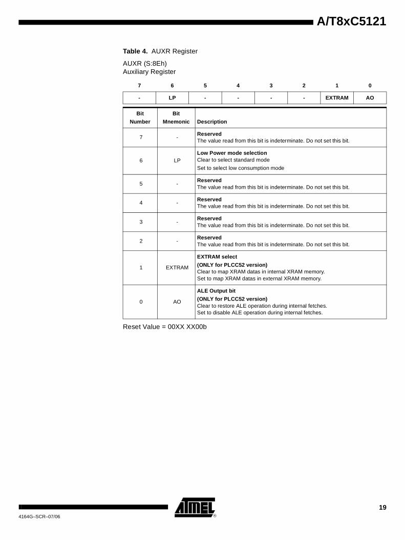
Table 4. AUXR Register
AUXR (S:8Eh)Auxiliary Register
Reset Value = 00XX XX00b
7 6 5 4 3 2 1 0
- LP - - - - EXTRAM AO
Bit
Number
Bit
Mnemonic Description
7 -ReservedThe value read from this bit is indeterminate. Do not set this bit.
6 LPLow Power mode selectionClear to select standard mode
Set to select low consumption mode
5 -ReservedThe value read from this bit is indeterminate. Do not set this bit.
4 -ReservedThe value read from this bit is indeterminate. Do not set this bit.
3 -ReservedThe value read from this bit is indeterminate. Do not set this bit.
2 -ReservedThe value read from this bit is indeterminate. Do not set this bit.
1 EXTRAM
EXTRAM select
(ONLY for PLCC52 version)Clear to map XRAM datas in internal XRAM memory.Set to map XRAM datas in external XRAM memory.
0 AO
ALE Output bit
(ONLY for PLCC52 version)Clear to restore ALE operation during internal fetches.Set to disable ALE operation during internal fetches.
194164G–SCR–07/06

Table 5. IE0 Register
IE0 Interrupt Enable Register (A8h)
Reset Value = 0XX0 0000b
7 6 5 4 3 2 1 0
EA - - ES ET1 EX1 ET0 EX0
Bit
Number
Bit
Mnemonic Description
7 EA
Enable All interrupt bit
Clear to disable all interrupts.Set to enable all interrupts.If EA = 1, each interrupt source is individually enabled or disabled by setting or clearing its interrupt enable bit.
6 -ReservedThe value read from this bit is indeterminate. Do not set this bit.
5 -ReservedThe value read from this bit is indeterminate. Do not set this bit.
4 ESSerial port Enable bit
Clear to disable serial port interrupt.Set to enable serial port interrupt.
3 ET1Timer 1 overflow interrupt Enable bit
Clear to disable Timer 1 overflow interrupt.Set to enable Timer 1 overflow interrupt.
2 EX1External interrupt 1 Enable bit
Clear to disable external interrupt 1.Set to enable external interrupt 1.
1 ET0Timer 0 overflow interrupt Enable bit
Clear to disable Timer 0 overflow interrupt.Set to enable Timer 0 overflow interrupt.
0 EX0External interrupt 0 Enable bit
Clear to disable external interrupt 0.Set to enable external interrupt 0.
20 A/T8xC51214164G–SCR–07/06

A/T8xC5121
Table 6. ISEL Register
ISEL (S:BAh)Interrupt Enable Register
Reset Value = 0X00 0000b
7 6 5 4 3 2 1 0
CPLEV - RXIT PRESIT OELEV OEEN RXEN PRESEN
Bit
Number
Bit
Mnemonic Description
7 CPLEV
Card presence detection level
This bit indicates which CPRES level will bring about an interruptSet this bit to indicate that Card Presence IT will appear if CPRES is at high level.
Clear this bit to indicate that Card Presence IT will appear if CPRES is at low level.
6 -ReservedThe value read from this bit is indeterminate. Do not set this bit.
5 PRESIT
Card presence detection interrupt flag
Set by hardware
Must be cleared by software
4 RXIT
Received data interrupt flag
Set by hardware
Must be cleared by software
3 OELEVOE/INT1 signal active levelSet this bit to indicate that high level is active.
Clear this bit to indicate that low level is active.
2 OEEN
OE/INT1 interrupt disable bit
Clear to disable INT1 interrupt
Set to enable INT1 interrupt
1 PRESENCard presence detection interrupt enable bitClear to disable the card presence detection interrupt coming from SCIB.Set to enable the card presence detection interrupt coming from SCIB.
0 RXENReceived data Interrupt enable bitClear to disable the RxD interrupt.Set to enable the RxD interrupt
214164G–SCR–07/06

Clock Management In order to optimize the power consumption and the execution time needed for a specifictask, an internal prescaler feature and a X2 feature have been implemented betweenthe oscillator and the CPU.
Functional Block Diagram
Figure 11. Clock Generation Diagram
If CKRL<>7 then:
If CKRL = 7 then:
CKRL Prescalor Factor
7 1
6 2
5 4
4 6
3 8
2 10
1 12
0 14
1
2
FOSC
1
2(7-CKRL)
CKRL = 7
X2
FCLK_Periph
FCLK_CPU
CKCON0
CKRL
FOSC
2x2
0
1
0
1Osc.
XTAL1
XTAL2
FCLK CPU–
FOSC
2 x2( )-----------------x 1
2 7 CKRL–( )-----------------------------------=
FCLK CPU–
Fosc
2x2--------------=
22 A/T8xC51214164G–SCR–07/06

A/T8xC5121
X2 Feature The T8xC5121 core needs only 6 clock periods per machine cycle. This feature called”X2” provides the following advantages:
• Divides frequency crystals by 2 (cheaper crystals) while keeping same CPU power.
• Saves power consumption while keeping same CPU power (oscillator power saving).
• Saves power consumption by dynamically dividing the operating frequency by 2 in operating and idle modes.
• Increases CPU power by 2 while keeping same crystal frequency.
In order to keep the original C51 compatibility, a divider by 2 is inserted between theXTAL1 signal and the main clock input of the core (phase generator). This divider maybe disabled by software.
Description The clock for the whole circuit and peripherals is first divided by two before being usedby the CPU core and the peripherals.
This allows any cyclic ratio to be accepted on XTAL1 input. In X2 mode, as this divider isbypassed, the signals on XTAL1 must have a cyclic ratio from 40 to 60%.
As shown in Figure 11, X2 bit is validated on the rising edge of the XTAL1÷2 to avoidglitches when switching from X2 to standard mode. Figure 12 shows the switching modewaveforms.
Figure 12. Mode Switching Waveforms
The X2 bit in the CKCON0 register (see Table 9) allows to switch (if CKRL=7) from 12clock periods per instruction to 6 clock periods and vice versa.
The T0X2, T1X2, UartX2, and WdX2 bits in the CKCON0 register (see Table 9) andSCX2 bit in the CKCON1 register (see Table 10) allow to switch from standard periph-eral speed (12 clock periods per peripheral clock cycle) to fast peripheral speed (6 clockperiods per peripheral clock cycle). These bits are active only in X2 mode.
More information about the X2 mode can be found in the application note "How to TakeAdvantage of the X2 Features in TS80C51 Microcontroller?".
XTAL1:2
XTAL1
CPU clock
X2 bit
X2 ModeSTD Mode STD Mode
FOSC
234164G–SCR–07/06

Clock Prescaler Before supplying the CPU and the peripherals, the main clock is divided by a factor 2 to30 to reduce the CPU power consumption. This factor is controlled with the CKRLregister.
Table 7. Examples of Factors
Clock Control Registers
Clock Prescaler Register This register is used to reload the clock prescaler of the CPU and peripheral clock.
Table 8. CKRL Register
CKRL - Clock Reload Register (97h)
Reset Value = XXXX 111Xb
XTAL (MHz) X2 CPU CKCON0 CKRL Value Prescaler FactorFCLK_CPU, FCLK_Periph
(MHz)
16 0 (reset mode) 07h 1 8
16 1 (X2 mode) 07h 1 16
16 1 07h 1 16
16 0 07h 1 8
16 0 06h 2 4
16 1 06h 2 8
7 6 5 4 3 2 1 0
- - - - CKRL CKRL CKRL -
Bit
Number
Bit
Mnemonic Description
7 - 4 -Reserved
The value read from this bit is indeterminate. Do not set this bit.
3 - 1 CKRL
Clock Reload Register
Prescaler value
XXXX 000Xb: CKRL=7 and Division factor equals 14
XXXX 110Xb: CKRL=6 and factor equals 2
XXXX 111Xb: CKRL=7 and division factor equals 1
0 -Reserved
The value read from this bit is indeterminate. Do not set this bit.
24 A/T8xC51214164G–SCR–07/06

A/T8xC5121
Table 9. CKCON0 Register
CKCON0 - Clock Control Register (8Fh)
Reset Value = X0X0 X000b
7 6 5 4 3 2 1 0
- WDX2 - SIX2 - T1X2 T0X2 X2
Bit
Number
Bit
Mnemonic Description
7 - Reserved
6 WDX2
Watchdog clock
(This control bit is validated when the CPU clock X2 is set; when X2 is low, this bit has no effect)Cleared to select 6 clock periods per peripheral clock cycle.
Set to select 12 clock periods per peripheral clock cycle.
5 - Reserved
4 SIX2
Enhanced UART clock (Mode 0 and 2)
(This control bit is validated when the CPU clock X2 is set; when X2 is low, this bit has no effect)Clear to select 6 clock periods per peripheral clock cycle.
Set to select 12 clock periods per peripheral clock cycle.
3 - Reserved
2 T1X2
Timer 1 clock
(This control bit is validated when the CPU clock X2 is set; when X2 is low, this bit has no effect)Clear to select 6 clock periods per peripheral clock cycle.
Set to select 12 clock periods per peripheral clock cycle
1 T0X2
Timer 0 clock
(This control bit is validated when the CPU clock X2 is set; when X2 is low, this bit has no effect)Clear to select 6 clock periods per peripheral clock cycle.
Set to select 12 clock periods per peripheral clock cycle
0 X2
CPU clock
Clear to select 12 clock periods per machine cycle (Standard mode) for CPU and all the peripherals.
Set to select 6 clock periods per machine cycle (X2 mode) and to enable the individual peripherals "X2" bits.
254164G–SCR–07/06

Table 10. CKCON1 Register
CKCON1 - Clock Control Register (AFh)
Reset Value = XXXX 0XXXb
7 6 5 4 3 2 1 0
- - - - SCX2 - - -
Bit
Number
Bit
Mnemonic Description
7 - Reserved
6 - Reserved
5 - Reserved
4 - Reserved
3 SCX2SCIB clockClear to select 6 clock periods per peripheral clock cycle.
Set to select 12 clock periods per peripheral clock cycle.
2 - Reserved
1 - Reserved
0 - Reserved
26 A/T8xC51214164G–SCR–07/06

A/T8xC5121
DC/DC Clock The DC/DC block needs a clock with a 50% duty cycle. The frequency must also respecta value between 3.68 MHz and 4 MHz. The first requirement imposes a divider in theclock path and the second constraint is solved with the use of a prescaler.
Figure 13. Functional Block Diagram
Clock Control Register This register is used to reload the clock prescaler of the DC/DC converter clock.
Table 11. DCCKPS Register
DCCKPS - DC/DC converter Reload Register (BFh)
Reset Value = XXXX XX11b
Clock Prescaler Before supplying the DC/DC block, the oscillator clock is divided by a factor 2 to 5 toadapt the clock needed by the DC/DC converter. This factor is controlled with theDCCKPS register.
The prescaler factor must be chosen to match the requirement range which is 4MHz.
Table 12. Examples of Factors
1FCLK_DC/DC
FOSC
FOSC
2 to 5
(2 to 5)
DCCKPS
Address BFh
7 6 5 4 3 2 1 0
- - - - - - DCCKPS DCCKPS
Bit
Number
Bit
Mnemonic Description
7:2 -Reserved
Do not use write those bits
1:0 DCCKPS
Clock Reload Register
Prescaler value
00b: Division factor equals 2
01b: division factor equals 3
10b: division factor equals 4
11b: division factor equals 5 (reset value which minimize the consumption)
XTAL (MHz) DCCKPS Value
Prescaler
Factor DC/DC Converter CLK (MHz)
8 00h 2 4
12 01h 3 4
14.756 02h 4 3.689
16 02h 4 4
20 03h 5 4
274164G–SCR–07/06

28 A/T8xC51214164G–SCR–07/06
A/T8xC5121
Smart Card Interface Block (SCIB)
Introduction The SCIB provides all signals to directly interface a smart card. Compliance with theISO7816, EMV’2000, GSM and WHQL standards has been certified.
Both synchronous (e.g. memory card) and asynchronous smart cards (e.g. micropro-cessor card) are supported. The component supplies the different voltages requested bythe smart card. The power-off sequence is directly managed by the SCIB.
The card presence switch of the smart card connector is used to detect card insertion orcard removal. In case of card removal, the SCIB de-activates the smart card using thede-activation sequence. An interrupt can be generated when a card is inserted orremoved.
Any malfunction is reported to the microcontroller (interrupt + control register).
The different operating modes are configured by internal registers.
Main Features • Support of ISO/IEC7816
• Character mode
• 1 transmit buffer + 1 receive buffer
• 11 bits ETU counter
• 9 bits guard time counter
• 24 bits waiting time counter
• Auto-character repetition on error signal detection in transmit mode
• Auto-error signal generation on parity error detection in receive mode
• Power-on and power-off sequence generation
• Manual mode to directly drive the card I/O
294164G–SCR–07/06
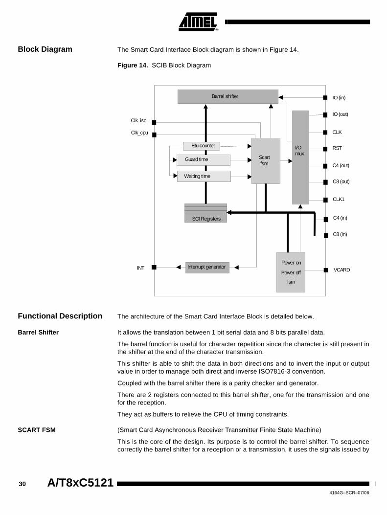
Block Diagram The Smart Card Interface Block diagram is shown in Figure 14.
Figure 14. SCIB Block Diagram
Functional Description The architecture of the Smart Card Interface Block is detailed below.
Barrel Shifter It allows the translation between 1 bit serial data and 8 bits parallel data.
The barrel function is useful for character repetition since the character is still present inthe shifter at the end of the character transmission.
This shifter is able to shift the data in both directions and to invert the input or outputvalue in order to manage both direct and inverse ISO7816-3 convention.
Coupled with the barrel shifter there is a parity checker and generator.
There are 2 registers connected to this barrel shifter, one for the transmission and onefor the reception.
They act as buffers to relieve the CPU of timing constraints.
SCART FSM (Smart Card Asynchronous Receiver Transmitter Finite State Machine)
This is the core of the design. Its purpose is to control the barrel shifter. To sequencecorrectly the barrel shifter for a reception or a transmission, it uses the signals issued by
Barrel shifter
SCI Registers
Scart fsm
Interrupt generator Power on Power off
fsm
I/O mux
IO (in)
IO (out)
CLK
RST
C4 (out)
Clk_iso
C8 (out)
CLK1
C4 (in)
C8 (in)
Waiting time counter
Guard time counter
Etu counter
VCARD INT
Clk_cpu
30 A/T8xC51214164G–SCR–07/06

A/T8xC5121
the different counters. One of the most important counters is the guard time counter thatgives time slots corresponding to the character frame.
It is enabled only in UART mode.
The transition from the receipt mode to the transmit mode is done automatically. Priorityis given to the transmission.
ETU Counter The ETU (Elementary Timing Unit) counter controls the working frequency of the barrelshifter, in fact, it generates the enable signal of the barrel shifter.
It is 11 bits wide and there is a special compensation mode activated with the most sig-nificant bit that allows non integer ETU value with a working clock equal to the cardclock .
But the decimal value is limited to a half clock cycle. In fact the bit duration is not fixed. Ittakes turns in n clock cycles and n-1 clock cycles. The character duration (10 bits) isalso equal to 10*(n+1/2) clock cycles.
This allows to reach the required precision of the character duration specified by theISO7816 standard.
example: F = 372 D = 32 = > ETU = 11.625 clock cycles.
ETU = (ETU[10-0] -0.5 * COMP)*f with ETU[10-0] = 12, COMP = 1 (bit 7 of SCETU1)
To achieve this clock rate we activated the compensation mode and we programmedthe ETU duration to 12 clock cycles.
The result will be a full character duration (10 bits) equal to 11.5 clock cycles.
Guard Time Counter The minimum time between the leading edge of the start bit of a character and the lead-ing edge of the start bit of the following character transmitted (Guard time) is controlledby one counter.
It is 9 bits wide and is incremented at the ETU rate.
Figure 15. Guard Time Counter
ETU Counter
SCGT1 SCGT0
GT[8:0]
Guard Time CounterTimeout
314164G–SCR–07/06

Waiting Time Counter (WT) The WT counter is a 24 bits down counter which can be loaded with the value containedin the SCWT2, SCWT1, SCWT0 registers. Its main purpose is time out signal genera-tion. It is 24 bits wide and is decremented at the ETU rate. The ETU counter acts as aprescaler (See Figure 16).
When the WT counter timeout, an interrupt is generated and the SCIB function islocked: reception and emission are disabled. It can be enabled by resetting the macro orreloading the counter.
Figure 16. Waiting Time Counter
The counter is loaded, if WTEN = 0, during the write of SCWT2 register.
This counter is available in both UART and manual modes. But the behaviour dependson the selected mode.
In manual mode, the WTEN signal controls the start of the counter (rising edge) and thestop of the counter (falling edge). After a time out of the counter, a falling edge onWTEN, a reload of SCWT2 and a rising edge of WTEN are necessary to start again thecounter and to release the SCIB macro. The reload of SCWT2 transfers all SCWT0,SCWT1 and SCWT2 registers to the WT counter.
In UART mode there is an automatic load on the start bit detection. This automatic loadis very useful for changing on-the-fly the Timeout value since there is a register to holdthe load value. This is the case, for example, when in T = 1 a launch is performed on theBWT Timeout on the start bit of the last transmitted character. But on the receipt of thefirst character an other time out value (CWT) must be used . For this, the new load valueof the waiting time counter must be loaded with CWT before the transmission of the lastcharacter. The reload of SCWT[2-0] with the new value occurs with WTEN = 1.
After a time out of the counter in UART mode, the restart is done as in manual mode.
The maximum interval between the start leading edge of a character and the start lead-ing edge of the next character is loaded in the SCWT2, SCWT1, SCWT0 registers.
In T = 1 mode, the CWT (character waiting time) or the BWT (block waiting time) areloaded in the same registers.
The maximum time between two consecutive start bit is WT[23:0] * ETU.
When used to check BWT according to ISO 7816, WT can be set between 971 and15728651.
ETU Counter WT CounterTimeout
SCWT2 SCWT1 SCWT0
WT[23:0]
LoadWTEN
Start bitUART
Write_SCWT2
32 A/T8xC51214164G–SCR–07/06

A/T8xC5121
Figure 17. T = 0 Mode
Figure 18. T = 1 Mode
Power-on and Power-off FSM In this state, the machine applies the signals on the smart card in accordance withISO7816 standard.
To be able to power-on the SCIB, the card presence is mandatory.
Removal of the smart card will automatically start the power-off sequence as describedin Figure 19.
Figure 19. SCI Deactivation Sequence after a Card Extraction
CHAR 1 CHAR 2
< WT
> GT
BLOC 1
CHAR 1 CHAR 2 CHAR n
BLOC 2
CHAR n+1 CHAR n+2 CHAR n+3
< CWT< BWT
< CWT
Transmission Reception
VCC
RST
CLK
IO
8 Clock Cycles
334164G–SCR–07/06
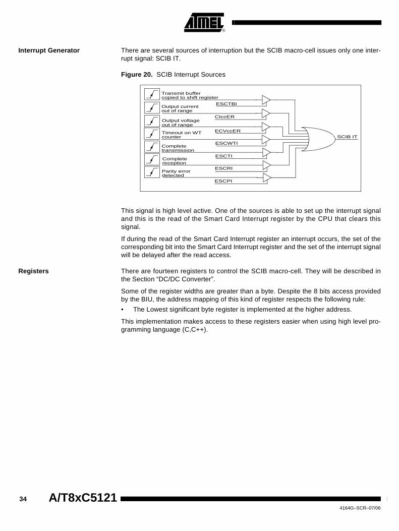
Interrupt Generator There are several sources of interruption but the SCIB macro-cell issues only one inter-rupt signal: SCIB IT.
Figure 20. SCIB Interrupt Sources
This signal is high level active. One of the sources is able to set up the interrupt signaland this is the read of the Smart Card Interrupt register by the CPU that clears thissignal.
If during the read of the Smart Card Interrupt register an interrupt occurs, the set of thecorresponding bit into the Smart Card Interrupt register and the set of the interrupt signalwill be delayed after the read access.
Registers There are fourteen registers to control the SCIB macro-cell. They will be described inthe Section “DC/DC Converter”.
Some of the register widths are greater than a byte. Despite the 8 bits access providedby the BIU, the address mapping of this kind of register respects the following rule:
• The Lowest significant byte register is implemented at the higher address.
This implementation makes access to these registers easier when using high level pro-gramming language (C,C++).
ESCTBI
CIccER
ESCWTI
ESCRI
ESCPI
ECVccER
Transmit buffercopied to shift register
Output currentout of range
Output voltageout of range
Timeout on WT counter
Completetransmission
Complete reception
Parity errordetected
SCIB IT
ESCTI
34 A/T8xC51214164G–SCR–07/06
A/T8xC5121
Other Features
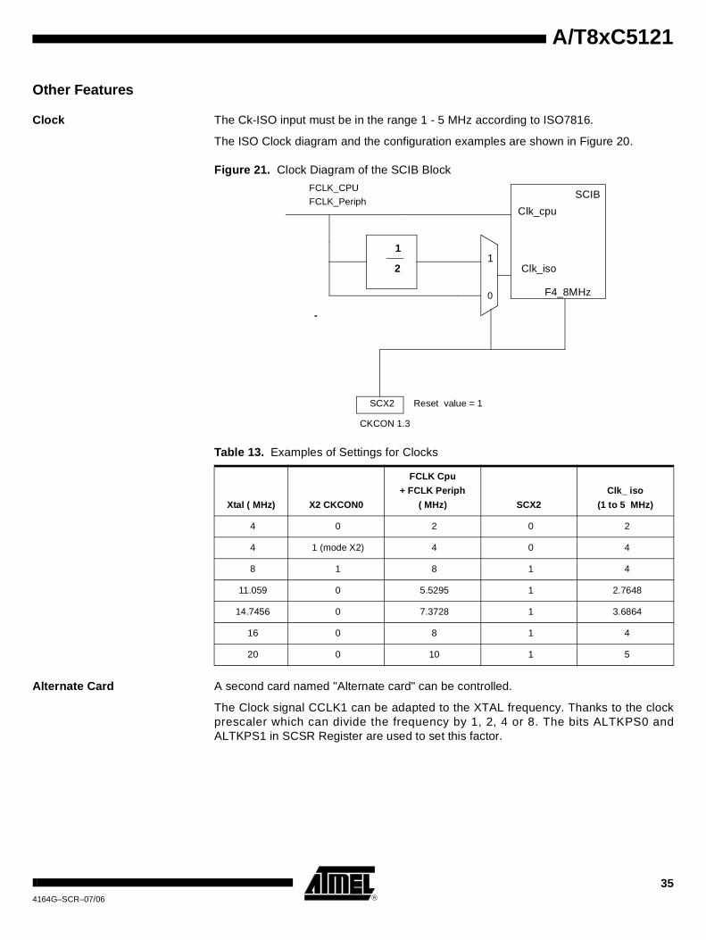
Clock The Ck-ISO input must be in the range 1 - 5 MHz according to ISO7816.
The ISO Clock diagram and the configuration examples are shown in Figure 20.
Figure 21. Clock Diagram of the SCIB Block
Table 13. Examples of Settings for Clocks
Alternate Card A second card named "Alternate card" can be controlled.
The Clock signal CCLK1 can be adapted to the XTAL frequency. Thanks to the clockprescaler which can divide the frequency by 1, 2, 4 or 8. The bits ALTKPS0 andALTKPS1 in SCSR Register are used to set this factor.
Xtal ( MHz) X2 CKCON0
FCLK Cpu
+ FCLK Periph
( MHz) SCX2
Clk_ iso
(1 to 5 MHz)
4 0 2 0 2
4 1 (mode X2) 4 0 4
8 1 8 1 4
11.059 0 5.5295 1 2.7648
14.7456 0 7.3728 1 3.6864
16 0 8 1 4
20 0 10 1 5
1
21
Clk_cpu
Clk_iso
SCIB
F4_8MHz0
SCX2
CKCON 1.3
Reset value = 1
FCLK_CPU
FCLK_Periph
354164G–SCR–07/06

Figure 22. Alternate Card
Card Presence Input The internal pull-up on Card Presence input can be disconnected in order to reduce theconsumption (CPRESRES, bit 3 in PMOD0).
In this case, an external resistor (typically 1 MΩ) must be externally tied to VCC.
CPRES input can generate an interrupt (see Interrupt system section).
The detection level can be selected.
SCIB Reset The SCICR register contains a reset bit. If set, this bit generates a reset of the SCI andits registers. Table 15 shows the SCIB registers that are reseted and their reset values.
Table 14. Reset Values for SCI Registers
SIM,SAM
CARD
Alternatecard
CVCCCRSTCIO
CCLK
FCK_IDLE 1
0
CCLK1
SCSR Reg.
PR3
SCSR Reg.
ALTKPS0,1 SCCLK1
FCK_IDLE
1, 2, 4 or 8
P3.6
Maincard
CPRES
Register Name SCIB Reset Value (Binary)
SCICR 0000 0000b
SCCON 0X00 0000b
SCISR 1000 0000b
SCIIR 0X00 0000b
SCIER 0X00 0000b
SCSR XXX0 1000b
SCTBUF 0000 0000b
SCRBUF 0000 0000b
SCETU1, SCETU0 XXX X001b, 0111 0100b (372)
SCGT1, SCGT0 XXXX XXX0b, 0000 1100b (12)
SCWT2, SCWT1, SCWT0 0000 0000b, 0010 0101b, 1000 0000b (9600)
36 A/T8xC51214164G–SCR–07/06

A/T8xC5121
DC/DC Converter The Smart Card supply voltage (CVCC) is generated by the integrated DC/DC converter.It is controlled by several registers:
• The register described in Section “SCICR Register” controls the CVCC voltage with bits CVcc0, CVcc1
• The register described in Section “SCCON Register”, switches ON/OFF the DC/DC converter with bit CARDVCC
• After the selection of the card voltage (CVcc[1:0]), the CARVCC bit is used to switch on the DC\DC converter. The CVccOK bit indicates that the card voltage is within the voltage range.
• It is mandatory to switch off the CVCC before entering in power-down mode.
374164G–SCR–07/06
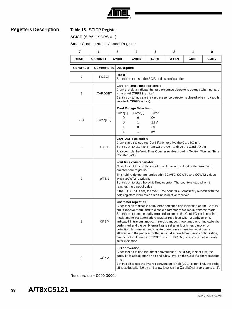
Registers Description Table 15. SCICR Register
SCICR (S:B6h, SCRS = 1)
Smart Card Interface Control Register
Reset Value = 0000 0000b
7 6 5 4 3 2 1 0
RESET CARDDET CVcc1 CVcc0 UART WTEN CREP CONV
Bit Number Bit Mnemonic Description
7 RESETResetSet this bit to reset the SCIB and its configuration
6 CARDDET
Card presence detector senseClear this bit to indicate the card presence detector is opened when no card is inserted (CPRES is high).Set this bit to indicate the card presence detector is closed when no card is inserted (CPRES is low).
5 - 4 CVcc[1:0]
Card Voltage Selection:
CVcc[1] CVcc[0] CVcc
0 0 0V
0 1 1.8V
1 0 3V
1 1 5V
3 UART
Card UART selectionClear this bit to use the Card I/O bit to drive the Card I/O pin. Set this bit to use the Smart Card UART to drive the Card I/O pin.
Also controls the Wait Time Counter as described in Section “Waiting Time Counter (WT)”
2 WTEN
Wait time counter enableClear this bit to stop the counter and enable the load of the Wait Time counter hold registers.
The hold registers are loaded with SCWT0, SCWT1 and SCWT2 values when SCWT2 is written.Set this bit to start the Wait Time counter. The counters stop when it reaches the timeout value.
If the UART bit is set, the Wait Time counter automatically reloads with the hold registers whenever a start bit is sent or received.
1 CREP
Character repetitionClear this bit to disable parity error detection and indication on the Card I/O pin in receive mode and to disable character repetition in transmit mode.Set this bit to enable parity error indication on the Card I/O pin in receive mode and to set automatic character repetition when a parity error is indicated in transmit mode. In receive mode, three times error indication is performed and the parity error flag is set after four times parity error detection. In transmit mode, up to three times character repetition is allowed and the parity error flag is set after five times (reset configuration, can be set at 4 using CREPSET bit in SCSR Register) consecutive parity error indication.
0 CONV
ISO conventionClear this bit to use the direct convention: b0 bit (LSB) is sent first, the parity bit is added after b7 bit and a low level on the Card I/O pin represents a “0”.Set this bit to use the inverse convention: b7 bit (LSB) is sent first, the parity bit is added after b0 bit and a low level on the Card I/O pin represents a “1”.
38 A/T8xC51214164G–SCR–07/06

A/T8xC5121
Table 16. SCCON Register
SCCON (S:ACh, SCRS = 0) Smart Card Contacts Register
Reset Value = 0X00 0000b
7 6 5 4 3 2 1 0
CLK - CARDC8 CARDC4 CARDIO CARDCLK CARDRST CARDVCC
Bit Number Bit Mnemonic Description
7 CLK
Card Clock SelectionClear this bit to use the CardClk bit (CARDCLK) to drive Card CLK pin.Set this bit to use XTAL signal to drive the Card CLK pin.
Note: internal synchronization avoids any glitch on the CLK pin when switching this bit.
6 -ReservedThe value read from this bit is indeterminate. Do not change this bit or write 0.
5 CARDC8Card C8
Clear this bit to drive a low level on the Card C8 pin.Set this bit to set a high level on the Card C8 pin.
4 CARDC4Card C4Clear this bit to drive a low level on the Card C4 pin.Set this bit to set a high level on the Card C4 pin.
3 CARDIO
Card I/OWhen the UART bit is cleared in SCICR Register, the value of this bit is driven to the Card I/O pin.
Then this pin can be used as a pseudo bi-directional I/O when this bit is set.
To be used as an input, this bit must contain a 1.
2 CARDCLKCard CLKWhen the CLK bit is cleared in SCCON Register, the value of this bit is driven to the Card CLK pin.
1 CARDRST
Card RSTClear this bit to drive a low level on the Card RST pin.Set this bit to set a high level on the Card RST pin.
Read is not allowed if VCARDOK=0
0 CARDVCC
Card VCC ControlClear this bit to desactivate the Card interface and set its power-off. The other bits of SCC register have no effect while this bit is cleared.Set this bit to power-on the Card interface. The activation sequence shall be handled by software.
394164G–SCR–07/06

Table 17. SCISR Register
SCISR (S:ADh, SCRS = 0) Smart Card UART Interface Status Register
Reset Value = 1000 0000b
7 6 5 4 3 2 1 0
SCTBE CARDIN CIccOVF CVccOK SCWTO SCTC SCRC SCPE
Bit Number
Bit Mnemonic Description
7 SCTBE
SCIB transmit buffer emptyThis bit is set by hardware when the Transmit Buffer is copied to the transmit shift register of the Smart Card UART.It is cleared by hardware when SCTBUF is written to.
6 CARDIN
Card presence statusThis bit is set when a card is detected (debouncing filter has to be done in software).It is cleared otherwise.
5 CIccOVF
ICC overflow on card
This bit is set when the current on card is above the limit
It shall be cleared by the hardware .
4 CVccOK
Card voltage statusThis bit is set when the output voltage is within the voltage range specified by CVcc field.It is cleared otherwise.
3 SCWTOSmart card wait TimeoutThis bit is set by hardware when the Smart card wait time counter times out.It shall be cleared by the reload of the counter or by the reset of the SCIB.
2 SCTC
Smart card transmitted characterThis bit is set by hardware when the Smart Card UART has transmitted a character.It shall be cleared by software after this register has been read.
1 SCRCSmart card received characterThis bit is set by hardware when the Smart Card UART has received a characterIt is cleared by hardware when SCBUF is read.
0 SCPESmart card parity errorThis bit is set at the same time as SCTI or SCRI if a parity error is detected.It shall be cleared by software after this register has been read.
40 A/T8xC51214164G–SCR–07/06

A/T8xC5121
Table 18. SCIIR Register
SCIIR (S:AEh, SCRS = 0) Smart Card UART Interrupt Identification Register (read only)
Reset Value = 0X00 0000b
7 6 5 4 3 2 1 0
SCTBI - CIccERR CVccERR SCWTI SCTI SCRI SCPI
Bit Number Bit Mnemonic Description
7 SCTBI
SCIB transmit buffer interruptThis bit is set by hardware when the Transmit Buffer is copied to the transmit shift register of the Smart Card UART.It is cleared by hardware when this register is read.
6 -ReservedThe value read from this bit is indeterminate. Do not change this bit or write 0.
5 CIccERRCard current statusThis bit is set when the output current goes out of the current range.It is cleared by hardware when this register is read.
4 CVccERR
Card voltage statusThis bit is set when the output voltage goes out of the voltage range specified by CVcc field.It is cleared by hardware when this register is read.
3 SCWTISmart card wait Timeout interruptThis bit is set by hardware when the Smart Card Timer 0 times out.It is cleared by hardware when this register is read.
2 SCTI
Smart card transmit interruptThis bit is set by hardware when the Smart Card UART completes a character transmission.It is cleared by hardware when this register is read.
1 SCRI
Smart card receive interruptThis bit is set by hardware when the Smart Card UART completes a character reception.It is cleared by hardware when this register is read.
0 SCPISmart card parity error interruptThis bit is set at the same time as SCTI or SCRI if a parity error is detected.It is cleared by hardware when this register is read.
414164G–SCR–07/06

Table 19. SCIER Register
SCIER (S:AEh, SCRS = 1) Smart Card UART Interrupt Enable Register
Reset Value = 0X00 0000b
7 6 5 4 3 2 1 0
ESCTBI - CIccER ECVccER ESCWTI ESCTI ESCRI ESCPI
Bit NumberBit
Mnemonic Description
7 ESCTBISmart Card UART Transmit Buffer Empty Interrupt EnableClear this bit to disable the Smart Card UART Transmit Buffer Empty interrupt.Set this bit to enable the Smart Card UART Transmit Buffer Empty interrupt.
6 -ReservedThe value read from this bit is indeterminate. Do not change this bit .
5 CIccERCard Current Error Interrupt EnableClear this bit to disable the Card Current Error interrupt.Set this bit to enable the Card Current Error interrupt.
4 ECVccERCard Voltage Error Interrupt EnableClear this bit to disable the Card Voltage Error interrupt.Set this bit to enable the Card Voltage Error interrupt.
3 ESCWTISmart Card Wait Timeout Interrupt EnableClear this bit to disable the Smart Card Wait timeout interrupt.Set this bit to enable the Smart Card Wait timeout interrupt.
2 ESCTISmart Card Transmit Interrupt EnableClear this bit to disable the Smart Card UART Transmit interrupt.Set this bit to enable the Smart Card UART Transmit interrupt.
1 ESCRISmart Card Receive Interrupt EnableClear this bit to disable the Smart Card UART Receive interrupt.Set this bit to enable the Smart Card UART Receive interrupt.
0 ESCPISmart Card Parity Error Interrupt EnableClear this bit to disable the Smart Card UART Parity Error interrupt.Set this bit to enable the Smart Card UART Parity Error interrupt.
42 A/T8xC51214164G–SCR–07/06

A/T8xC5121
Table 20. SCSR Register
SCSR (S:ABh) Smart Card Selection Register
Reset Value = XXX0 1000b
Table 21. SCTBUF Register
SCTBUF (S:AA, write-only, SCRS = 0) Smart Card Transmit Buffer Register
Reset Value = 0000 0000b
7 6 5 4 3 2 1 0
- - - CREPSEL ALTKPS1 ALTKPS0 SCCLK1 SCRS
Bit Number
Bit Mnemonic Description
7 - Reserved
6 - Reserved
5 - Reserved
4 CREPSEL
Character repetition selection
Clear this bit to select 5 times repetition before parity error indication
Set this bit to select 4 times repetition before parity error indication
3-2ALTKPS1
ALTKPS0
Alternate Card Clock prescaler factor
00ALTKPS = 0: prescaler factor equals 1
01ALTKPS = 1: prescaler factor equals 2
10ALTKPS = 2: prescaler factor equals 4 (reset value)
11ALTKPS = 3: prescaler factor equals 8
1 SCCLK1
Alternate card clock selection
Set to select the prescaled clock (CCLK1)
Clear to select the standard port configuration (P3.6)
0 SCRSSmart card register selectionThe SCRS bit selects which set of the SCIB registers is accessed.
7 6 5 4 3 2 1 0
Bit Number Bit Mnemonic Description
– –Can store a new byte to be transmitted on the I/O pin when SCTBE is set.Bit ordering on the I/O pin depends on the Convention (see SCICR Register).
434164G–SCR–07/06

Table 22. SCRBUF Register
SCRBUF (S:AA read-only, SCRS = 1) Smart Card Receive Buffer Register
Reset Value = 0000 0000b
Table 23. SCETU1 Register
SCETU1 (S:ADh, SCRS = 1) Smart Card ETU Register 1
Reset Value = 0XXX X001b
7 6 5 4 3 2 1 0
– – – – – – – –
Bit Number
Bit Mnemonic Description
– –Provides the byte received from the I/O pin when SCRI is set.Bit ordering on the I/O pin depends on the Convention (see SCICR Register).
7 6 5 4 3 2 1 0
COMP – – – – ETU10 ETU9 ETU8
Bit Number
Bit Mnemonic Description
7 COMP
CompensationClear this bit when no time compensation is needed (i.e. when the ETU to Card CLK period ratio is close to an integer with an error less than 1/4 of Card CLK period).Set this bit otherwise and reduce the ETU period by 1 Card CLK cycle for even bits.
6-3 –ReservedThe value read from these bits is indeterminate. Do not change these bits .
2-0 ETU[10:8]ETU MSBUsed together with the ETU LSB (see SCETU0 Register).
44 A/T8xC51214164G–SCR–07/06

A/T8xC5121
Table 24. SCETU0 Register
SCETU0 (S:ACh, SCRS = 1) Smart Card ETU Register 0
Reset Value = 0111 0100b
Table 25. SCGT1 Register
SCGT1 (S:B5h, SCRS = 1) Smart Card Transmit Guard Time Register 1
Reset Value = XXXX XXX0b
Table 26. SCGT0 Register
SCGT0 (S:B4h, SCRS = 1) Smart Card Transmit Guard Time Register 0
Reset Value = 0000 1100b
7 6 5 4 3 2 1 0
ETU7 ETU6 ETU5 ETU4 ETU3 ETU2 ETU1 ETU0
Bit Number
Bit Mnemonic Description
7-0 ETU[7:0]
ETU LSBThe Elementary Time Unit is (ETU[10:0] - 0.5*COMP)/f, where f is the Card CLK frequency.According to ISO7816, ETU[10:0] can be set between 11 and 2047.The default reset value of ETU[10:0] is 372 (F = 372, D = 1).
7 6 5 4 3 2 1 0
– – – – – – – GT8
Bit Number
Bit Mnemonic Description
7-1 –ReservedThe value read from these bits is indeterminate. Do not change these bits .
0 GT8Transmit Guard Time MSBUsed together with the Transmit Guard Time LSB (see SCGT0 Register).
7 6 5 4 3 2 1 0
GT7 GT6 GT5 GT4 GT3 GT2 GT1 GT0
Bit Number
Bit Mnemonic Description
7-0 GT[7:0]
Transmit Guard Time LSBThe minimum time between two consecutive start bits in transmit mode is GT[8:0] * ETU.According to ISO 7816, GT can be set between 11 and 266 (11 to 254+12 ETU).
454164G–SCR–07/06

Table 27. SCWT2 Register
SCWT2 (S:B6h, SCRS = 0) Smart Card Character/Block Wait Time Register 2
Reset Value = 0000 0000b
Table 28. SCWT1 Register
SCWT1 (S:B5h, SCRS = 0) Smart Card Character/Block Wait Time Register 1
Reset Value = 0010 0101b
Table 29. SCWT0 Register
SCWT0 (S:B4h, SCRS = 0) Smart Card Character/Block Wait Time Register 0
Reset Value = 1000 0000b
7 6 5 4 3 2 1 0
WT23 WT22 WT21 WT20 WT19 WT18 WT17 WT16
Bit Number
Bit Mnemonic Description
7-0 WT[23:16]Wait Time Byte 2Used together with WT[15:0] (see SCWT0 Register).
7 6 5 4 3 2 1 0
WT15 WT14 WT13 WT12 WT11 WT10 WT9 WT8
Bit Number
Bit Mnemonic Description
7-0 WT[15:8]Wait Time Byte 1Used together with WT[23:16] and WT[7:0] (see SCWT0 Register).
7 6 5 4 3 2 1 0
WT7 WT6 WT5 WT4 WT3 WT2 WT1 WT0
Bit Number
Bit Mnemonic Description
7-0 WT[7:0]
Wait Time Byte 0
WT[23:0] is the reload value of the Wait Time counter WTC.The WTC is a general-purpose Timer 0. It is using the ETU clock and is controlled by the WTEN bit (see Section “Waiting Time Counter (WT)”).
When UART bit of SCICR Register is set, the WTC is automatically reloaded at each start bit of the UART. It is used to check the maximum time between to consecutive start bits.
46 A/T8xC51214164G–SCR–07/06

A/T8xC5121
Interrupt System The T8xC5121 has a total of 6 interrupt vectors: four external interrupts (INT0, INT1/OE,CPRES, RxD), two Timer 0 interrupts (Timer 0s 0 and 1), serial port interrupt and SmartCard Interface interrupt. These interrupts are shown in Figure 23.
Figure 23. Interrupt Control System
Each of the interrupt sources can be individually enabled or disabled by setting or clear-ing a bit in the Interrupt Enable register (see Figure 32). This register also contains aglobal disable bit, which must be cleared to disable all interrupts at once.
Each interrupt source can also be individually programmed to one of four priority levelsby setting or clearing a bit in the Interrupt Priority register (see Figure 36) and in theInterrupt Priority High register (see Figure 38). Table 30 shows the bit values and prioritylevels associated with each combination.
Table 30. Priority Level Bit Values
0
3
InterruptPollingSequence
TIRI
TF0
INT0
TF1
IPH0, IPL0
IE0
0
3
0
3
0
3
0
3
0
3
IndividualEnable
GlobalEnable
Low PriorityInterrupt
High PriorityInterrupt
INT1/OE
CPRES
Rxd
RXEN
SCI
RXIT
CPLEV
EX0
ET0
EX1
ET1
ES
ESCI
OEEN0
1IE1
1
0
0
1
PRESEN0
1
OELEVIT1
IT0
TCON reg.
TCON Reg.
PRESIT
The selection bitsexcept IT1 (TCON)are in ISEL Reg.
IPH1, IPL1
IPH.x IP.x Interrupt Level Priority
0 0 0 (Lowest)
0 1 1
1 0 2
1 1 3 (Highest)
474164G–SCR–07/06

A low-priority interrupt can be interrupted by a high priority interrupt, but not by anotherlow-priority interrupt. A high-priority interrupt can’t be interrupted by any other interruptsource.
If two interrupt requests of different priority levels are received simultaneously, therequest of higher priority level is serviced. If interrupt requests of the same priority levelare received simultaneously, an internal polling sequence determines which request isserviced. Thus within each priority level there is a second priority structure determinedby the polling sequence.
Table 31. Interrupt Vector Addresses
INT1 Interrupt Vector The INT1 interrupt is multiplexed with the three following inputs:
• INT1/OE: Standard 8051 interrupt input
• Rxd: Received data on UART
• CPRES: Insertion or removall of the main card
The setting configurations for each input is detailed below:
INT1/OE Input This interrupt input is active under the following conditions:
• It must be enabled thanks to OEEN Bit (ISEL Register)
• It can be active on a level or falling edge: thanks to IT1 Bit (TCON Register)
• If level triggering selection is set, the active level 0 or 1 can be selected with OELEV Bit (ISEL Register)
The Bit IE1 (TCON Register) is set by hardware when external interrupt detected. It iscleared when interrupt is processed.
Rxd Input A second vector interrupt input is the reception of a character. UART Rx input can gen-erate an interrupt if enabled with Bit RXEN (ISEL.0). The global enable bits EX1 and EAmust also be set.
Then, the Bit RXIT (ISEL Register) is set by hardware when a low level is detected onP3.0/RXD input.
CPRES Input The third input is the detection of a level change on CPRES input (P1.2). This input cangenerate an interrupt if enabled with PRESEN (ISEL.1), EX1 (IE0.2) and EA (IE0.7) Bits.
This detection is done according to the level selected with Bit CPLEV (ISEL.7).
Then the Bit PRESIT (ISEL.5) is set by hardware when the triggering conditions aremet. This Bit must be cleared by software.
Interrupt Source Vector Address
IE0 0003h
TF0 000Bh
IE1 & RxIt & PrIt 0013h
TF1 001Bh
RI & TI 0023h
SCI 0053h
48 A/T8xC51214164G–SCR–07/06

A/T8xC5121
Table 32. IE0 Register
Reset Value = 0XX0 0000bBit addressable
7 6 5 4 3 2 1 0
EA - - ES ET1 EX1 ET0 EX0
Bit
Number
Bit
Mnemonic Description
7 EA
Enable All interrupt bitClear to disable all interrupts.Set to enable all interrupts.If EA = 1, each interrupt source is individually enabled or disabled by setting or clearing its interrupt enable bit.
6 -ReservedThe value read from this bit is indeterminate. Do not set this bit.
5 -ReservedThe value read from this bit is indeterminate. Do not set this bit.
4 ESSerial port Enable bitClear to disable serial port interrupt.Set to enable serial port interrupt.
3 ET1Timer 1 overflow interrupt Enable bitClear to disable Timer 1 overflow interrupt.Set to enable Timer 1 overflow interrupt.
2 EX1External interrupt 1 Enable bitClear to disable external interrupt 1.Set to enable external interrupt 1.
1 ET0Timer 0 overflow interrupt Enable bitClear to disable Timer 0 overflow interrupt.Set to enable Timer 0 overflow interrupt.
0 EX0External interrupt 0 Enable bitClear to disable external interrupt 0.Set to enable external interrupt 0.
494164G–SCR–07/06

Table 33. IE1 Register
Reset Value = XXXX 0XXXb
7 6 5 4 3 2 1 0
- - - - ESCI - - -
Bit
Number
Bit
Mnemonic Description
7 -ReservedThe value read from this bit is indeterminate. Do not set this bit.
6 -ReservedThe value read from this bit is indeterminate. Do not set this bit.
5 -ReservedThe value read from this bit is indeterminate. Do not set this bit.
4 -ReservedThe value read from this bit is indeterminate. Do not set this bit.
3 ESCISCI Interrupt EnableClear to disable the SCI interrupt.Set to enable the SCI interrupt.
2 -ReservedThe value read from this bit is indeterminate. Do not set this bit.
1 -ReservedThe value read from this bit is indeterminate. Do not set this bit.
0 -ReservedThe value read from this bit is indeterminate. Do not set this bit.
50 A/T8xC51214164G–SCR–07/06

A/T8xC5121
Table 34. TCON RegisterTCON (S:88h)Timer 0/Counter Control Register
Reset Value = 0000 0000b
7 6 5 4 3 2 1 0
TF1 TR1 TF0 TR0 IE1 IT1 IE0 IT0
Bit Number
Bit Mnemonic Description
7 TF1
Timer 1 Overflow flagCleared by the hardware when processor vectors to interrupt routine.Set by the hardware on Timer 0/Counter overflow when Timer 1 register overflows.
6 TR1Timer 1 Run Control bitClear to turn off Timer 0/Counter 1.Set to turn on Timer 0/Counter 1.
5 TF0
Timer 0 Overflow flagCleared by the hardware when processor vectors to interrupt routine.Set by the hardware on Timer 0/Counter overflow when Timer 0 register overflows.
4 TR0Timer 0 Run Control bitClear to turn off Timer 0/Counter 0.Set to turn on Timer 0/Counter 0.
3 IE1Interrupt 1 Edge flagCleared by the hardware when interrupt is processed if edge-triggered (see IT1).Set by the hardware when external interrupt is detected on the INT1 pin.
2 IT1Interrupt 1 Type Control bitClear to select low level active (level triggered) for external interrupt 1 (INT1).Set to select falling edge active (edge triggered) for external interrupt 1.
1 IE0Interrupt 0 Edge flagCleared by the hardware when interrupt is processed if edge-triggered (see IT0).Set by the hardware when external interrupt is detected on INT0 pin.
0 IT0Interrupt 0 Type Control bitClear to select low level active (level triggered) for external interrupt 0 (INT0).Set to select falling edge active (edge triggered) for external interrupt 0.
514164G–SCR–07/06

Table 35. ISEL Register
Reset Value = 0000 0100b
7 6 5 4 3 2 1 0
CPLEV OEIT PRESIT RXIT OELEV OEEN PRESEN RXEN
Bit
Number
Bit
Mnemonic Description
7 CPLEV
Card presence detection level
This bit indicates which CPRES level will bring about an interruptSet this bit to indicate that Card Presence IT will appear if CPRES is at high level.
Clear this bit to indicate that Card Presence IT will appear if CPRES is at low level.
6 -ReservedThe value read from this bit is indeterminate. Do not set this bit.
5 PRESIT
Card presence detection interrupt flag
Set by hardware
Must be cleared by software
4 RXIT
Received data interrupt flag
Set by hardware
Must be cleared by software
3 OELEVOE/INT1 signal active levelSet this bit to indicate that high level is active.
Clear this bit to indicate that low level is active.
2 OEEN
OE/INT1 Interrupt Disable bit
Clear to disable INT1 interrupt
Set to enable INT1 interrupt
1 PRESENCard presence detection Interrupt Enable bitClear to disable the card presence detection interrupt coming from SCIB.Set to enable the card presence detection interrupt coming from SCIB.
0 RXEN
Received data Interrupt Enable bitClear to disable the RxD interrupt.Set to enable the RxD interrupt (a minimal bit width of 0.1 ms is required to wake up from Power-Down).
52 A/T8xC51214164G–SCR–07/06

A/T8xC5121
Table 36. IPL0 Register
Reset Value = XXX0 0000bBit addressable
7 6 5 4 3 2 1 0
- - - PSL PT1L PX1L PT0L PX0L
Bit
Number
Bit
Mnemonic Description
7 -ReservedThe value read from this bit is indeterminate. Do not set this bit.
6 -ReservedThe value read from this bit is indeterminate. Do not set this bit.
5 -ReservedThe value read from this bit is indeterminate. Do not set this bit.
4 PSLSerial port Priority bitRefer to PSH for priority level.
3 PT1LTimer 1 overflow interrupt Priority bitRefer to PT1H for priority level.
2 PX1LExternal interrupt 1 Priority bitRefer to PX1H for priority level.
1 PT0LTimer 0 overflow interrupt Priority bitRefer to PT0H for priority level.
0 PX0LExternal interrupt 0 Priority bitRefer to PX0H for priority level.
534164G–SCR–07/06

Table 37. IPL1 Register
Reset Value = XXXX 0XXXbBit addressable
7 6 5 4 3 2 1 0
- - - - PSCIL - - -
Bit
Number
Bit
Mnemonic Description
7 -ReservedThe value read from this bit is indeterminate. Do not set this bit.
6 -ReservedThe value read from this bit is indeterminate. Do not set this bit.
5 -ReservedThe value read from this bit is indeterminate. Do not set this bit.
4 -ReservedThe value read from this bit is indeterminate. Do not set this bit.
3 PSCILReservedThe value read from this bit is indeterminate. Do not set this bit.
2 -ReservedThe value read from this bit is indeterminate. Do not set this bit.
1 -ReservedThe value read from this bit is indeterminate. Do not set this bit.
0 -ReservedThe value read from this bit is indeterminate. Do not set this bit.
54 A/T8xC51214164G–SCR–07/06

A/T8xC5121
Table 38. IPH0 Register
Reset Value = XXX0 0000b
7 6 5 4 3 2 1 0
- - - PSH PT1H PX1H PT0H PX0H
Bit
Number
Bit
Mnemonic Description
7 -ReservedThe value read from this bit is indeterminate. Do not set this bit.
6 -ReservedThe value read from this bit is indeterminate. Do not set this bit.
5 -ReservedThe value read from this bit is indeterminate. Do not set this bit.
4 PSH
Serial port Priority High bit
PSH PS Priority Level0 0 Lowest0 11 01 1 Highest
3 PT1H
Timer 1 overflow interrupt Priority High bit
PT1H PT1 Priority Level0 0 Lowest0 11 01 1 Highest
2 PX1H
External interrupt 1 Priority High bit
PX1H PX1 Priority Level0 0 Lowest0 11 01 1 Highest
1 PT0H
Timer 0 overflow interrupt Priority High bit
PT0H PT0 Priority Level0 0 Lowest0 11 01 1 Highest
0 PX0H
External interrupt 0 Priority High bit
PX0 HPX0 Priority Level0 0 Lowest0 11 01 1 Highest
554164G–SCR–07/06

Table 39. IPH1 Register
Reset Value = XXXX 0XXXb
7 6 5 4 3 2 1 0
- - - - PSCIH - - -
Bit
Number
Bit
Mnemonic Description
7 -ReservedThe value read from this bit is indeterminate. Do not set this bit.
6 -ReservedThe value read from this bit is indeterminate. Do not set this bit.
5 -ReservedThe value read from this bit is indeterminate. Do not set this bit.
4 -ReservedThe value read from this bit is indeterminate. Do not set this bit.
3 PSCIH
SCI Interrupt Priority level most significant bitPSCIH PSCIL Priority level0 0 Lowest0 11 01 1 Highest priority
2 -ReservedThe value read from this bit is indeterminate. Do not set this bit.
1 -ReservedThe value read from this bit is indeterminate. Do not set this bit.
0 -ReservedThe value read from this bit is indeterminate. Do not set this bit.
56 A/T8xC51214164G–SCR–07/06
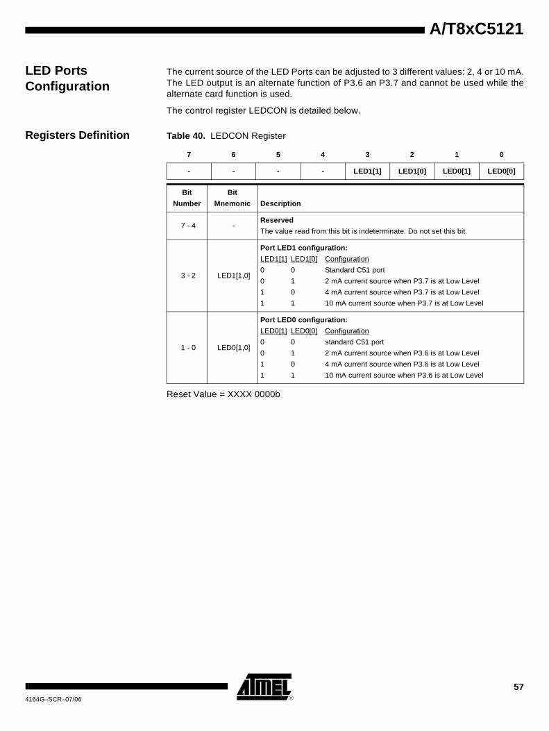
57
A/T8xC5121
4164G–SCR–07/06
LED Ports Configuration
The current source of the LED Ports can be adjusted to 3 different values: 2, 4 or 10 mA.The LED output is an alternate function of P3.6 an P3.7 and cannot be used while thealternate card function is used.
The control register LEDCON is detailed below.
Registers Definition Table 40. LEDCON Register
Reset Value = XXXX 0000b
7 6 5 4 3 2 1 0
- - - - LED1[1] LED1[0] LED0[1] LED0[0]
Bit
Number
Bit
Mnemonic Description
7 - 4 -Reserved
The value read from this bit is indeterminate. Do not set this bit.
3 - 2 LED1[1,0]
Port LED1 configuration:
LED1[1] LED1[0] Configuration
0 0 Standard C51 port
0 1 2 mA current source when P3.7 is at Low Level
1 0 4 mA current source when P3.7 is at Low Level
1 1 10 mA current source when P3.7 is at Low Level
1 - 0 LED0[1,0]
Port LED0 configuration:
LED0[1] LED0[0] Configuration
0 0 standard C51 port
0 1 2 mA current source when P3.6 is at Low Level
1 0 4 mA current source when P3.6 is at Low Level
1 1 10 mA current source when P3.6 is at Low Level

Dual Data Pointer T8xC5121 contains a Dual Data Pointer accelerating data memory block moves. TheStandard 80C52 Data Pointer is a 16-bit value that is used to address off-chip data RAMor peripherals. In T8xC5121, the standard 16-bit data pointer is called DPTR andlocated at SFR location 82H and 83H. The second Data Pointer named DPTR1 islocated at the same address than the previous one. The DPTR select bit (DPS / bit0)chooses the active pointer and it is located into the AUXR1 register. It should be ser-viced in those sections of code that will periodically be executed within the time requiredto prevent a WDT reset. The user switches between data pointers by toggling the LSB of the AUXR1. The incre-ment (INC) is a solution for this. All DPTR-related instructions use the currently selectedDPTR for any activity. Therefore only one instruction is required to switch from a sourceto a destination address. Using the Dual Data Pointer saves code and resources whenmoves of blocks need to be accomplished.
The second Data Pointer can be used to address the on-chip XRAM.
Table 41. DPL Register
DPL - Low Byte of DPTR1 (82h)
Reset value = 0000 0000b
Table 42. DPH Register
DPH - High Byte of DPTR1 (83h)
Reset value = 0000 0000b
7 6 5 4 3 2 1 0
- - - - - - - -
7 6 5 4 3 2 1 0
- - - - - - - -
58 A/T8xC51214164G–SCR–07/06

A/T8xC5121
Table 43. AUXR1 Register
AUXR1 - Dual Pointer Selection Register (A2h)
Reset value = XXXX XXX0b
7 6 5 4 3 2 1 0
- - - - - - - DPS
Bit
Number
Bit
Mnemonic Description
7 -ReservedThe value read from this bit is indeterminate. Do not set this bit.
6 -ReservedThe value read from this bit is indeterminate. Do not set this bit.
5 -ReservedThe value read from this bit is indeterminate. Do not set this bit.
4 -ReservedThe value read from this bit is indeterminate. Do not set this bit.
3 -ReservedThe value read from this bit is indeterminate. Do not set this bit.
2 -ReservedThe value read from this bit is indeterminate. Do not set this bit.
1 -ReservedThe value read from this bit is indeterminate. Do not set this bit.
0 DPSData pointer 1Clear to select DPTR0 as Data Pointer.
Set to select DPTR1 as Data Pointer.
594164G–SCR–07/06

Memory Management
Program Memory All the T8xC5121 versions implement 16 Kbytes of ROM memory, 256 Bytes RAM and256 Bytes XRAM.
The hardware configuration byte and the split of internal memory spaces depends onthe product and is detailed below.
ROM Configuration Byte Table 44. ROM Configuration Byte Hardware Register
The BLJRB depends of the product version:
• 1: ROM mask version
• 0: EEPROM/CRAM versions
This bit defines if, after reset, either the Customer ROM program or the Bootloader pro-gram is executed (for In System programming).
Program ROM Lock Bits The program Lock system protects the on-chip program against software piracy.
The T8xC5121 products are delivered with the highest protection level.
Table 45. T8xC5121 Products Protection Level
P = Programmed
7 6 5 4 3 2 1 0
- BLJRB - - - - -
Bit
Number
Bit
Mnemonic Description
7 Reserved
6 BLJRB
Bootloader Jump RAM Bit
Set to configure User Code in ROM
Clear to configure Bootlader in ROM
5-0 Reserved
Program Lock Bits Protection Description
Security
Level LB1 LB2
3 P P
SSOP24 version:
Read function is disabled.But checksum control is still enabled
PLCC52 version:
MOVC instruction executed from external program memory are disabled from fetching code bytes from internal memory,
EA is sampled and latched on reset.
But checksum control is still enabled.
External execution is possible.
60 A/T8xC51214164G–SCR–07/06

A/T8xC5121
Memory Mapping In the products versions, the following internal spaces are defined:
• RAM
• XRAM
• CRAM: 16 KBytes Program RAM Memory
• ROM
The specific accesses from/to these memories are:
• XRAM: if the bit RPS in RCON (described below) is reset, MOVX instructions address the XRAM space.
• CRAM: if the bit RPS in RCON is set, MOVX instructions address the CRAM space.
Table 46. RCON Register
Reset Value = XXXX 0XXXb
T89C5121 Flash ROM Version Three memory blocks are implemented
• An internal serial EEPROM can be loaded from external with the application program.
• The ROM memory contains the Bootloader program. The entry point is located at address F800h. The lower 14K Bytes between address C000h and F7FFh is, also, used for the Bootloader program.
• The CRAM is the application program memory. This memory is mapped in the External RAM space. The bit RPS in RCON (SFR address 0D1h) is set to map the CRAM space during MOVX instructions
For first programming or an update, the program can be downloaded in the internalEEPROM (and in the CRAM) from an external device:
• Either an external EEPROM if detected
• or from a host through RS232 serial communication.
For this purpose, an In-System Programming (ISP) is supplied in a Bootloader. ThisBootloader is program masked in ROM space.
The Hardware Byte BLJRB value is 0.
As described on page 7, after Reset, the Bootloader program is executed.
7 6 5 4 3 2 1 0
- - RPS
Bit
Number
Bit
Mnemonic Description
7-4 -ReservedThe value read from this bit is indeterminate. Do not set this bit.
3 RPS
CRAM space map bit
Set to map the CRAM space during MOVX instructions
Clear to map the Data space during MOVX. This bit has priority over the EXTRAM bit.
2-0 -ReservedThe value read from this bit is indeterminate. Do not set this bit.
614164G–SCR–07/06

If a serial communication device (as described above: TWI or RS232) is detected, theprogram download its content in the internal EEPROM and in CRAM.
Else, the program is internally downloaded from the internal EEPROM into the programCRAM memory (16 Kbytes)
Then, in the two cases, the Bootloader executes a Long Jump at address 0000h whichinitializes the Program counter at the lower address (0000h) of the executable CRAM.
Figure 24. CRAM with ROM and EEPROM Memory Mappings
T85C121 Code RAM Version Two memory blocks are implemented:
• The ROM memory contains the Bootloader program.
• The CRAM is the Application program memory.
After Reset, the program is downloaded, as described in last paragraph, from either anexternal EEPROM or from an host connected on RS232 serial link into the programCRAM memory of 16 Kbytes. Then the Program Counter is set at address 0000h of theCRAM space and the program is executed.
16 Kbytes
256 bytes0000h
3FFFh
CRAM XRAM RAMROM
FFFFh
F800h
C000h
entry point
Bootloader
256 bytes
62 A/T8xC51214164G–SCR–07/06

A/T8xC5121
Figure 25. CRAM and ROM Mappings
T83C5121 with Mask ROM Version
In this version, the customer program is masked in 16 Kbytes ROM.
• The customer program is masked in ROM during the final production phase. The ROM size will be determined at mask generation process depending of the program size.
In-System Programming The In-System Programming (ISP) mode is only implemented in the following productversions:
• EEPROM version
• CRAM version
(The ROM product version is masked with the customer program and does not needISP mode)
The ISP is used to download an Application program in the device and to run it.
The communication protocols which are implemented are: UART and TWI.
Hardware Interface The hardware in relation with the two communication protocols is detailed below:
• TWI protocol
• Serial protocol
16K bytes
0000h
3FFFh
CRAM XRAM RAMROM
FFFFh
C000hBootloader
F800h entry point
256 bytes 256 bytes
634164G–SCR–07/06
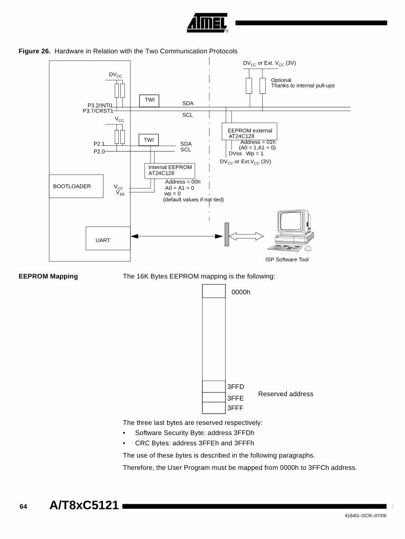
Figure 26. Hardware in Relation with the Two Communication Protocols
EEPROM Mapping The 16K Bytes EEPROM mapping is the following:
The three last bytes are reserved respectively:
• Software Security Byte: address 3FFDh
• CRC Bytes: address 3FFEh and 3FFFh
The use of these bytes is described in the following paragraphs.
Therefore, the User Program must be mapped from 0000h to 3FFCh address.
EEPROM external
TWI
DVCC or Ext. VCC (3V)
Internal EEPROMAT24C128
VCCVSS
DVCC or Ext.VCC (3V)
A0 = A1 = 0wp = 0
SDASCL
TWI
OptionalThanks to internal pull-ups
DVCC
VCC
P2.1P2.0
(A0 = 1,A1 = 0)DVss Wp = 1
AT24C128
(default values if not tied)
P3.2/INT0
UART
BOOTLOADER
Address = 01h
Address = 00h
ISP Software Tool
SDA
SCLP3.7/CRST1
3FFD
3FFE3FFF
0000h
Reserved address
64 A/T8xC51214164G–SCR–07/06

A/T8xC5121
Bootloader Functional Diagram
As described in Section “ROM Configuration Byte”, page 60a ROM bit BLJRB (BootLoader Jump ROM Bit) defines which product version is. The Bootloader program ismapped in ROM space from address C000h up to FFFFh and the entry point is locatedat address F800h.
Figure 27. Bootloader Flowchart
ACK?E2PROM at 00
ACK?E2PROM at 01
Error: No TWI or serial device detected
U Characterreceived on UART
? Serial communication is detected thanks to
Time Elapsed
Internal E2PROM (at 00) is detected
BootloaderExecution
RESET
ROM programExecution
BLJRB = 1ROM Bit
ROM
RAM+ROM RAM+ROM (Pre-prod: Application Program)
F800h
versions:
ROM
ROM
0000h
External E2PROM (at 01) is detected
(Prod)RAM,ROM,EEPROM
A serial code is sent on RD pin (P3.7)
Versions:
SSB & P3.7 testTWI
ext.bypassed? bypassed?
SSB & P3.6 testUART bypassed
bypassed?
Program is downloaded fromExternal EEPROM into internal
An ISP Software can be used froma PC to program the part.Atmel FLIP software is available
Program is downloaded from internal EEPROM in CRAM andexecuted
EEPROM and CRAMand executed.
RD port = Error code = 22h
Autobaud feature (Table52)
654164G–SCR–07/06

In-System Programming Timings
The download from the internal EEPROM to CRAM is executed after 4 seconds whenoperating at 12 MHz frequency.
Protection Mechanisms
Transfer Checks In order to verify that the transfers are free of errors, a CRC check is implemented dur-ing the download of the program in CRAM.
This test is done at the end of the 16K space programming.
As detailed in the next algorithms:
• in ISP mode, if CRC test pass, a character Y is returned before the CRLF characters else a character Z is retuned.
• in download mode, a serial data AA is sent on P3.7 port and CRAM is not executed.
For this purpose, the user program must include in the two last upper bytes (address3FFEh and 3FFFh) the CRC of the previous bytes (calculated from the address 0000hto 3FFFDh).
The following frames are examples including the CRC in the two last upper bytes:
• FF 03 C0 21 04 00 00 08 07 02 08 02 2D DB (CRC = 2DDBh)
• FF 03 80 21 02 04 00 0A 03 06 C0 A8 70 01 E3 3D (CRC = E33Dh)
• FF 03 C0 21 02 01 00 10 02 06 00 00 00 00 05 06 00 00 76 55 49 AC (CRC = 49ACh)
The CRC algorithm is the following :
***************************************************************************************************
Uint16 compute_crc (Uint16 W)
{
UcharC;
W&=(Uint16)0x00FF;
for (C=(Uchar)8;C;C--)
{
if ((Uchar)W&(Uchar)1)
{
W>>=1;
W^=(Uint16)0x8408;
}
else
W>>=1;
return W;
Data Bytes
2 Bytes CRC
HSB LSB
Address: 3FFE,3FFF
66 A/T8xC51214164G–SCR–07/06

A/T8xC5121
}
void generate_crc_in_frame(void)
{
checksum_tx=(Uint16) FFFFh; /* init of the crc variable */
/* loop which compute for each byte (data_byte) to load */
checksum_tx=compute_crc((Uint16)data_byte^checksum_tx)^(checksum_tx>>8);
/* end of loop */
checksum=~checksum_tx; /* inverts the checksum, so the check will calculate
the CRC of all the datas and */
/* will find a constant value = F0B8
which is the CRC_REF const. of the Bootloader */
write_frame(LOW_BYTE(checksum)); /* writes the LOW_BYTE of the CRC first */
write_frame(HIGH_BYTE(checksum)); /* writes the HIGH_BYTE */
}
***************************************************************************************************
Table 47. Synthesis of Transfer Protection Mechanisms
Notes: 1. The transfer of SSB Byte is also secured by CRC as the CRC is computed on all the16K data.
2. If a Bad transfer has occurred in the Internal EEPROM (CRC is bad), as the CRCcheck is finally done at the end of CRAM programming, application program will NOTbe executed after any Reset.
Read/Write Protection
Lock Byte In order to protect the content of the internal EEPROM, a Software Security Byte (SSB)defines two security levels:
• level 0: SSB = 0xFF: Write and Read are allowed
• level 1: SSB = 0xFE: Write is disabled
• level 2: SSB = 0xFC: Write and Read are disabled
This SSB Byte is located at address 3FFDh.
When the level 2 is set, the command to set level 1 is disabled. The security levels canonly be increased.
Source Target Check
MCU CRAMCRC computed during CRAM Write operation: if error an error code is applied on P3.7 and Code execution by LJMP000 is not done.
Intern. EEP MCU This Read operation is secured by the Write sequence described above
MCU Intern. EEPSame protection as in first row above because CRAM is written in sequence after each page programming of EEP
Ext. EEP MCU Same as above as data are transferred to EEP INT and then to CRAM
674164G–SCR–07/06

The only mean to remove the security level 2 is to send a Full Chip Erase command.
Table 48. Synthesis of Security Mechanisms
Configuration Bits The Bootloader tests that TWI components are connected as slave components on theTWI external bus and later in the algorithm if characters are received on the UART input.This default configuration can be changed, after a first programming, in order:
– to disable new programming in download mode from external serial EEPROM to disable ISP programming using UART and
– to avoid any conflict with the target hardware on external TWI bus or UART.
This can be configured with the two higher bits of the SSB Byte detailed in the previousparagraph.
The bit 7 is used to bypass (if 0) the External TWI Acknowledge test.
The bit 6 is used to bypass (if 0) the UART receipt test.
These two bypass modes can be disabled if a level 0 is applied on, respectively, P3.5and P3.6 pins. This allows to force and use ISP even if the device has been configuredas programmed device.
Source Function Protection
Internal EEPROM
WriteThe first protection level of the SSB Byte IN the internal EEPROM protects against ISP Write command
Internal EEPROM
ReadThe second protection level of the SSB Byte IN the internal EEPROM protects against ISP Read commands
CRAM WriteThe first protection level of the SSB Byte IN the internal EEPROM protects against ISP Write command in CRAM
CRAM ReadThe second protection level of the SSB Byte IN the CRAM protects against ISP Read commands
Data Bytes SSB
Address 3FFD
68 A/T8xC51214164G–SCR–07/06

A/T8xC5121
Table 49. Valid Software Security Byte Values
UART Protocol
Overview The serial protocol used is described below.
Physical Layer The UART is used to transmit information with the following configuration:
• Character: 8-bit data
• Parity: none
• Stop: 1 bit
• Flow control: none
• Baudrate: autobaud is performed by the bootloader to compute the baudrate chosen by the host.
Datas and Limits As described in Section “Transfer Checks”, the downloaded program include the CRCvalues in the last two upper bytes of the 16K bytes space.
An update of a part of the 16K program cannot be done because the CRC value wouldhave to be updated with a value which depends of the actual value of the rest of theprogram.
So the Program function of the PC Software Tool include the individual program com-mands (with 64 data bytes) from address 0000h to address 3FFFh.
Frame Description The Serial Protocol is based on the Intel Hex-type records.
Intel Hex records consist of ASCII characters used to represent hexadecimal values andare summarized below:
Table 50. Intel Hex Type Frame
• Record Mark:
– Record Mark is the start of frame. This field must contain’:’.
• Reclen:
– Reclen specifies that the number of bytes of information or data that follow the Record Type field of the record.
• Load Offset:
– Load Offset specifies the 16-bit starting load offset of the data bytes, therefore this field is used only for Program Data Record (see Table 51).
SSB Values Functions
FE No bypass and level1 security
FC No bypass and level2 security
BF,BE,BC UART bypass and security levels
7F,7E,7C External TWI bypass and security levels
3F,3E,3C UART and Ext. TWI bypass
Record Mark ‘:’ Reclen Load Offset Record Type Data or Info Checksum
1-byte 1-byte = 40h 2-byte 1-byte 64-byte 1-byte
694164G–SCR–07/06

• Record Type:
– Record Type specifies the command type. This field is used to interpret the remaining information within the frame. The encoding for all the current record types are described in Table 51.
• Data/Info:
– Data/Info is a 64 bytes length field. It consists of 64 bytes encoded as pairs of hexadecimal digits. The meaning of data depends on the Record Type.
• Checksum:
– The two’s complement of the 8-bit bytes that result from converting each pair of ASCII hexadecimal digits to one byte of binary, and including the Reclen field to and including the last byte of the Data/Info field. Therefore, the sum of all the ASCII pairs in a record after converting to binary, from the Reclen field to and including the Checksum field, is zero.
Notes: 1. A data byte is represented by two ASCII characters.2. When the field Load Offset is not used, it should be coded as 2 bytes (00h 00h).
Command Description Table 51. Frame Description
Command Command Name data[0] data[1] Command Effect
00h Program Data Program 64 Data Bytes
01h End Of File - - End of File
03h Write Function
07h
05h
05h
03h
00h
01h
01h
Full Chip Erase
Program SSB level1
Program SSB level2
LJMP(data[2],data[3]) (LJMP0000h)
04h Display Function
Data[0:1] = start address
Data [2:3] = end address
Data[4] = 00h -> Display data
Data[4] = 01h -> Blank check
Data[4] = 03h -> Display CRAM
Display Data
05h Read Function07h
0Fh
00h
00h
Read SSB
Read Bootloader Version
06h Direct Load of Baud Rate HSB LSB Not implemented
70 A/T8xC51214164G–SCR–07/06

A/T8xC5121
Autobaud The ISP feature allows a wide range of baud rates in the user application. It is alsoadaptable to a wide range of oscillator frequencies. This is accomplished by measuringthe bit-time of a single bit in a received character. This information is then used to pro-gram the baud rate in terms of timer counts based on the oscillator frequency. The ISPfeature requires that an initial character (an uppercase U) be sent to the T8xC5121 toestablish the baud rate. Table show the autobaud capability.
Protection Mechanisms
Transfer Checks Table 53. Synthesis of the Communication Protection Mechanisms
Notes: 1. The transfer of SSB Byte is also secured by CRC as the CRC is computed on all the16K data.
2. If a bad transfer has occurred in the Internal EEPROM (CRC is bad), as the CRCcheck is finally done at the end of CRAM programming, application program will NOTbe executed after any Reset.
Security Table 54. Synthesis of the Security Mechanisms
Table 52. Autobaud Performances
Frequency (MHz)Baudrate (kHz) 6.176 8 11.0592 12 14.3 14.7456 16
9600 OK OK OK OK OK OK -
19200 OK - OK OK Ok OK OK
38400 - OK OK OK OK OK
57600 - - OK - OK OK -
115200 - - - - - OK -
Source Target Check
UART ISP MCUChecksum included in commands is tested with calculated checksum: if bad, X echo returned to ISP
MCU CRAMCRC computed during CRAM Write operation: if error an error code is applied on P3.7. Error code’Z’ is returned to ISP.
MCU Intern. EEPSame protection as above because CRAM is written in sequence after each page programming of EEP
Source Target Case Protection
UART ISP Intern. EEP Read accessSSB level 2 must be set (done, if selected, at ISP Programming or Ext EEP Download)
UART ISP CRAM Read accessSSB level 2 IN CRAM must be set (SSB is downloaded from Int EEP after Reset)
UART ISP Intern. EEPPartial Programming which would not fit with old CRC
SSB level 1 must be set (done, if selected, at ISP Programming or Ext EEP Download)
Then the EEP must be, first, erased before reprogramming.
Programming is done on all the memory space
714164G–SCR–07/06

UART ISP Intern. EEP Programming SSB level 1 must be set (done, if selected, at ISP Programming or Ext EEP Donwload)
UART ISP CRAM Program accessSSB level 1 IN Int EEP protects as, first, the Int EEP is programmed before CRAM
UART ISPSSB in EEP and CRAM
level 2 to level 1 Protected by Bootloader
UART ISPSSB in EEP and CRAM
level 1 to level 0 Protected by Bootloader
Source Target Case Protection
72 A/T8xC51214164G–SCR–07/06

A/T8xC5121
Timers/Counters
Introduction The T8xC5121 implements two general-purpose, 16-bit Timer 0s/Counters. Althoughthey are identified as Timer 0, Timer 1, you can independently configure each to operatein a variety of modes as a Timer 0 or as an event Counter. When operating as a Timer 0,a Timer 0/Counter runs for a programmed length of time, then issues an interruptrequest. When operating as a Counter, a Timer 0/Counter counts negative transitionson an external pin. After a preset number of counts, the Counter issues an interruptrequest.
The Timer 0 registers and associated control registers are implemented as addressableSpecial Function Registers (SFRs). Two of the SFRs provide programmable control ofthe Timer 0s as follows:
• Timer 0/Counter mode control register (TMOD) and Timer 0/Counter control register (TCON) control respectively Timer 0 and Timer 1.
The various operating modes of each Timer 0/Counter are described below.
Timer 0/Counter Operations
For example, a basic operation is Timer 0 registers THx and TLx (x = 0, 1) connected incascade to form a 16-bit Timer 0. Setting the run control bit (TRx) in the TCON register(see Figure 55) turns the Timer 0 on by allowing the selected input to increment TLx.When TLx overflows it increments THx and when THx overflows it sets the Timer 0 over-flow flag (TFx) in the TCON register. Setting the TRx does not clear the THx and TLxTimer 0 registers. Timer 0 registers can be accessed to obtain the current count or toenter preset values. They can be read at any time but the TRx bit must be cleared topreset their values, otherwise the behavior of the Timer 0/Counter is unpredictable.
The C/Tx# control bit selects Timer 0 operation or Counter operation by selecting thedivided-down system clock or the external pin Tx as the source for the counted signal.The TRx bit must be cleared when changing the operating mode, otherwise the behaviorof the Timer 0/Counter is unpredictable.For Timer 0 operation (C/Tx# = 0), the Timer 0 register counts the divided-down systemclock. The Timer 0 register incremented once every peripheral cycle.
Exceptions are the Timer 0 2 Baud Rate and Clock-Out modes in which the Timer 0 reg-ister is incremented by the system clock divided by two.
For Counter operation (C/Tx# = 1), the Timer 0 register counts the negative transitionson the Tx external input pin. The external input is sampled during every S5P2 state. TheProgrammer’s Guide describes the notation for the states in a peripheral cycle. Whenthe sample is high in one cycle and low in the next one, the Counter is incremented. Thenew count value appears in the register during the next S3P1 state after the transitionhas been detected. Since it takes 12 states (24 oscillator periods) to recognize a nega-tive transition, the maximum count rate is 1/24 of the oscillator frequency. There are norestrictions on the duty cycle of the external input signal, but to ensure that a given levelis sampled at least once before it changes, it should be held for at least one full periph-eral cycle.
734164G–SCR–07/06

Timer 0 Timer 0 functions as either a Timer 0 or an event Counter in four operating modes.Figure 28 through Figure 31 show the logic configuration of each mode.
Timer 0 is controlled by the four lower bits of the TMOD register (see Figure 56) and bits0, 1, 4 and 5 of the TCON register (see Figure 55). The TMOD register selects themethod of Timer 0 gating (GATE0), Timer 0 or Counter operation (T/C0#) and the oper-ating mode (M10 and M00). The TCON register provides Timer 0 control functions:overflow flag (TF0), run control bit (TR0), interrupt flag (IE0) and interrupt type control bit(IT0).For normal Timer 0 operation (GATE0 = 0), setting TR0 allows TL0 to be incrementedby the selected input. Setting GATE0 and TR0 allows external pin INT0 to control Timer 0operation.
Timer 0 overflow (count rolls over from all 1s to all 0s) sets the TF0 flag and generatesan interrupt request.
It is important to stop the Timer 0/Counter before changing modes.
Mode 0 (13-bit Timer 0) Mode 0 configures Timer 0 as a 13-bit Timer 0 which is set up as an 8-bit Timer 0 (TH0register) with a module-32 prescaler implemented with the lower five bits of the TL0 reg-ister (see Figure 28). The upper three bits of the TL0 register are indeterminate andshould be ignored. Prescaler overflow increments the TH0 register.
Figure 28. Timer 0/Counter x (x = 0 or 1) in Mode 0
Mode 1 (16-bit Timer 0) Mode 1 configures Timer 0 as a 16-bit Timer 0 with the TH0 and TL0 registers con-nected in a cascade (see Figure 29). The selected input increments the TL0 register.
TRxTCON reg
TFxTCON reg
0
1
GATExTMOD reg
OverflowTimer 0 xInterruptRequest
C/Tx#TMOD reg
TLx(5 bits)
THx(8 bits)
INTx#
Tx
FCLK_Periph
74 A/T8xC51214164G–SCR–07/06

A/T8xC5121
Figure 29. Timer 0/Counter x (x = 0 or 1) in Mode 1
Mode 2 (8-bit Timer 0 with Auto-Reload)
Mode 2 configures Timer 0 as an 8-bit Timer 0 (TL0 register) that automatically reloadsfrom the TH0 register (see Figure 30). TL0 overflow sets the TF0 flag in the TCON reg-ister and reloads TL0 with the contents of TH0, which is preset by the software. Whenthe interrupt request is serviced, the hardware clears TF0. The reload leaves TH0unchanged. The next reload value may be changed at any time by writing it to the TH0register.
Figure 30. Timer 0/Counter x (x = 0 or 1) in Mode 2
Mode 3 (Two 8-bit Timer 0s) Mode 3 configures Timer 0 so that registers TL0 and TH0 operate as 8-bit Timer 0s (seeFigure 31). This mode is provided for applications requiring an additional 8-bit Timer 0 orCounter. TL0 uses the Timer 0 control bits C/T0# and GATE0 in the TMOD register, andTR0 and TF0 in the TCON register in the normal manner. TH0 is locked into a Timer 0function (counting FUART) and takes over use of the Timer 1 interrupt (TF1) and run con-trol (TR1) bits. Thus, operation of Timer 1 is restricted when Timer 0 is in mode 3.
TRxTCON reg
TFxTCON reg
0
1
GATExTMOD reg
OverflowTimer 0 xInterruptRequest
C/Tx#TMOD reg
TLx(8 bits)
THx(8 bits)
INTx#
Tx
FCLK_Periph
TRxTCON reg
TFxTCON reg
0
1
GATExTMOD reg
OverflowTimer 0 xInterruptRequest
C/Tx#TMOD reg
TLx(8 bits)
THx(8 bits)
INTx#
Tx
FCLK_Periph
754164G–SCR–07/06

Figure 31. Timer 0/Counter 0 in Mode 3: Two 8-bit Counters
TR0TCON.4
TF0TCON.5
INT0
0
1
GATE0TMOD.3
OverflowTimer 0InterruptRequest
C/T0#TMOD.2
TL0(8 bits)
TR1TCON.6
TH0(8 bits) TF1
TCON.7
OverflowTimer 1InterruptRequest
T0
FCLK_Periph
FCLK_Periph
76 A/T8xC51214164G–SCR–07/06

A/T8xC5121
Timer 1 Timer 1 is identical to Timer 0 except for Mode 3 which is a hold-count mode. The fol-lowing comments help to understand the differences:
• Timer 1 functions as either a Timer 0 or an event Counter in the three operating modes. Figure 28 through Figure 30 show the logical configuration for modes 0, 1, and 2. Mode 3 of Timer 1 is a hold-count mode.
• Timer 1 is controlled by the four high-order bits of the TMOD register (see Figure 56) and bits 2, 3, 6 and 7 of the TCON register (see Figure 55). The TMOD register selects the method of Timer 0 gating (GATE1), Timer 0 or Counter operation (C/T1#) and the operating mode (M11 and M01). The TCON register provides Timer 1 control functions: overflow flag (TF1), run control bit (TR1), interrupt flag (IE1) and the interrupt type control bit (IT1).
• Timer 1 can serve as the Baud Rate Generator for the Serial Port. Mode 2 is best suited for this purpose.
• For normal Timer 0 operation (GATE1 = 0), setting TR1 allows TL1 to be incremented by the selected input. Setting GATE1 and TR1 allows external pin INT1 to control Timer 0 operation.
• Timer 1 overflow (count rolls over from all 1s to all 0s) sets the TF1 flag and generates an interrupt request.
• When Timer 0 is in mode 3, it uses Timer 1’s overflow flag (TF1) and run control bit (TR1). For this situation, use Timer 1 only for applications that do not require an interrupt (such as a Baud Rate Generator for the Serial Port) and switch Timer 1 in and out of mode 3 to turn it off and on.
• It is important to stop the Timer 0/Counter before changing modes.
Mode 0 (13-bit Timer 0) Mode 0 configures Timer 1 as a 13-bit Timer 0, which is set up as an 8-bit Timer 0 (TH1register) with a modulo-32 prescaler implemented with the lower 5 bits of the TL1 regis-ter (see Figure 28). The upper 3 bits of TL1 register are ignored. Prescaler overflowincrements the TH1 register.
Mode 1 (16-bit Timer 0) Mode 1 configures Timer 1 as a 16-bit Timer 0 with TH1 and TL1 registers connected incascade (see Figure 29). The selected input increments the TL1 register.
Mode 2 (8-bit Timer 0 with Auto-Reload)
Mode 2 configures Timer 1 as an 8-bit Timer 0 (TL1 register) with automatic reload fromthe TH1 register on overflow (see Figure 30). TL1 overflow sets the TF1 flag in theTCON register and reloads TL1 with the contents of TH1, which is preset by the soft-ware. The reload leaves TH1 unchanged.
Mode 3 (Halt) Placing Timer 1 in mode 3 causes it to halt and hold its count. This can be used to haltTimer 1 when the TR1 run control bit is not available i.e., when Timer 0 is in mode 3.
774164G–SCR–07/06

Registers Table 55. TCON RegisterTCON (S:88h) - Timer 0/Counter Control Register
Reset Value = 0000 0000b
7 6 5 4 3 2 1 0
TF1 TR1 TF0 TR0 IE1 IT1 IE0 IT0
Bit Number
Bit Mnemonic Description
7 TF1
Timer 1 Overflow flagCleared by the hardware when processor vectors to interrupt routine.Set by the hardware on Timer 0/Counter overflow when Timer 1 register overflows.
6 TR1Timer 1 Run Control bitClear to turn off Timer 0/Counter 1.Set to turn on Timer 0/Counter 1.
5 TF0
Timer 0 Overflow flagCleared by the hardware when processor vectors to interrupt routine.Set by the hardware on Timer 0/Counter overflow when Timer 0 register overflows.
4 TR0Timer 0 Run Control bitClear to turn off Timer 0/Counter 0.Set to turn on Timer 0/Counter 0.
3 IE1Interrupt 1 Edge flagCleared by the hardware when interrupt is processed if edge-triggered (see IT1).Set by the hardware when external interrupt is detected on the INT1 pin.
2 IT1Interrupt 1 Type Control bitClear to select low level active (level triggered) for external interrupt 1 (INT1).Set to select falling edge active (edge triggered) for external interrupt 1.
1 IE0Interrupt 0 Edge flagCleared by the hardware when interrupt is processed if edge-triggered (see IT0).Set by the hardware when external interrupt is detected on INT0 pin.
0 IT0Interrupt 0 Type Control bitClear to select low level active (level triggered) for external interrupt 0 (INT0).Set to select falling edge active (edge triggered) for external interrupt 0.
78 A/T8xC51214164G–SCR–07/06

A/T8xC5121
Reset Value = 0000 0000b
Table 56. TMOD RegisterTMOD (S:89h) - Timer 0/Counter Mode Control Registers
7 6 5 4 3 2 1 0
GATE1 C/T1# M11 M01 GATE0 C/T0# M10 M00
Bit Number Bit Mnemonic Description
7 GATE1Timer 1 Gating Control bitClear to enable Timer 1 whenever TR1 bit is set.Set to enable Timer 1 only while INT1 pin is high and TR1 bit is set.
6 C/T1#Timer 1 Counter/Timer 0 Select bitClear for Timer 0 operation: Timer 1 counts the divided-down system clock.Set for Counter operation: Timer 1 counts negative transitions on external pin T1.
5 M11 Timer 1 Mode Select bitsM11 M01 Operating mode 0 0 Mode 0:8-bit Timer 0/Counter (TH1) with 5-bit prescaler (TL1). 0 1 Mode 1:16-bit Timer 0/Counter. 1 0 Mode 2:8-bit auto-reload Timer 0/Counter (TL1). Reloaded from TH1 at overflow. 1 1 Mode 3:Timer 1 halted. Retains count.
4 M01
3 GATE0Timer 0 Gating Control bitClear to enable Timer 0 whenever TR0 bit is set.Set to enable Timer 0/Counter 0 only while INT0 pin is high and TR0 bit is set.
2 C/T0#Timer 0 Counter/Timer 0 Select bitClear for Timer 0 operation: Timer 0 counts the divided-down system clock.Set for Counter operation: Timer 0 counts negative transitions on external pin T0.
1 M10 Timer 0 Mode Select bitM10 M00 Operating mode 0 0 Mode 0:8-bit Timer 0/Counter (TH0) with 5-bit prescaler (TL0). 0 1 Mode 1:16-bit Timer 0/Counter 1 0 Mode 2:8-bit auto-reload Timer 0/Counter (TL0). Reloaded from TH0 at overflow. 1 1 Mode 3:TL0 is an 8-bit Timer 0/Counter.TH0 is an 8-bit Timer 0 using Timer 1’s TR0 and TF0 bits.
0 M00
794164G–SCR–07/06

Table 57. TH0 RegisterTH0 (S:8Ch) - Timer 0 High Byte Register.
Reset Value = 0000 0000b
Table 58. TL0 RegisterTL0 (S:8Ah) - Timer 0 Low Byte Register.
Reset Value = 0000 0000b
Table 59. TH1 RegisterTH1 (S:8Dh) - Timer 1 High Byte Register.
Reset Value = 0000 0000b
Table 60. TL1 RegisterTL1 (S:8Bh) - Timer 1 Low Byte Register.
Reset Value = 0000 0000b
7 6 5 4 3 2 1 0
Bit Number
Bit Mnemonic Description
7:0 High Byte of Timer 0
7 6 5 4 3 2 1 0
Bit Number
Bit Mnemonic Description
7:0 Low Byte of Timer 0
7 6 5 4 3 2 1 0
Bit Number
Bit Mnemonic Description
7:0 High Byte of Timer 1
7 6 5 4 3 2 1 0
Bit Number
Bit Mnemonic Description
7:0 Low Byte of Timer 1
80 A/T8xC51214164G–SCR–07/06

A/T8xC5121
Serial I/O Port The serial I/O port is entirely compatible with the serial I/O port in the 80C52. It provides both synchronous and asynchronous communication modes. It operates asan Universal Asynchronous Receiver and Transmitter (UART) in three full-duplexmodes (Modes 1, 2 and 3). Asynchronous transmission and reception can occur simul-taneously and at different baud rates.
Serial I/O port includes the following enhancements:
• Framing error detection and Automatic Address Recognition
• Internal Baud Rate Generator
Figure 32. Serial I/O UART Port Block Diagram
Framing Error Detection Framing bit error detection is provided for the three asynchronous modes. To enable theframing bit error detection feature, set SMOD0 bit in PCON register.
Figure 33. Framing Error Block Diagram
When this feature is enabled, the receiver checks each incoming data frame for a validstop bit. An invalid stop bit may result from noise on the serial lines or from simultaneoustransmission by two CPUs. If a valid stop bit is not found, the Framing Error bit (FE) inSCON register bit is set.
Software may examine FE bit after each reception to check for data errors. Once set,only software or a reset clear FE bit. Subsequently received frames with valid stop bitscannot clear FE bit. When FE feature is enabled, RI rises on stop bit instead of the lastdata bit (See Figure 34 and Figure 35).
Write SBUF
RI TI
Transmitter
SBUFReceiver
IB Bus
Mode 0 Transmit
ReceiveShift register
Load SBUF
Read SBUF
Interrupt RequestSerial Port
TXD
RXD
SBUF
RITIRB8TB8RENSM2SM1SM0/FE
IDLPDGF0GF1POF-SMOD0SMOD1
To UART framing error control
SM0 to UART mode control
Set FE bit if stop bit is 0 (framing error)
814164G–SCR–07/06

Figure 34. UART Timings in Mode 1
Figure 35. UART Timings in Modes 2 and 3
Automatic Address Recognition
The automatic address recognition feature is enabled when the multiprocessor commu-nication feature is enabled (SM2 bit in SCON register is set).
Implemented in hardware, automatic address recognition enhances the multiprocessorcommunication feature by allowing the serial port to examine the address of eachincoming command frame. Only when the serial port recognizes its own address, thereceiver sets RI bit in SCON register to generate an interrupt. This ensures that the CPUis not interrupted by command frames addressed to other devices.
If desired, you may enable the automatic address recognition feature in mode 1. In thisconfiguration, the stop bit takes the place of the ninth data bit. Bit RI is set only when thereceived command frame address matches the device’s address and is terminated by avalid stop bit.
To support automatic address recognition, a device is identified by a given address anda broadcast address.
Note: The multiprocessor communication and automatic address recognition features cannotbe enabled in mode 0 (i.e., setting SM2 bit in SCON register in mode 0 has no effect).
Given Address Each device has an individual address that is specified in SADDR register; the SADENregister is a mask byte that contains don’t care bits (defined by zeros) to form thedevice’s given address. The don’t care bits provide the flexibility to address one or moreslaves at a time. The following example illustrates how a given address is formed.
Data Byte
RISMOD0 = X
StopBit
StartBit
RXD D7D6D5D4D3D2D1D0
FESMOD0 = 1
RISMOD0 = 0
Data Byte NinthBit
StopBit
StartBit
RXD D8D7D6D5D4D3D2D1D0
RISMOD0 = 1
FESMOD0 = 1
82 A/T8xC51214164G–SCR–07/06

A/T8xC5121
To address a device by its individual address, the SADEN mask byte must be 11111111b.For example:
SADDR0101 0110bSADEN1111 1100b
Given0101 01XXb
The following is an example of how to use given addresses to address different slaves:Slave A:SADDR1111 0001b
SADEN1111 1010b
Given1111 0X0Xb
Slave B:SADDR1111 0011bSADEN1111 1001b
Given1111 0XX1b
Slave C:SADDR1111 0011bSADEN1111 1101b
Given1111 00X1b
The SADEN byte is selected so that each slave may be addressed separately.For slave A, bit 0 (the LSB) is a don’t care bit; for slaves B and C, bit 0 is a 1. To commu-nicate with slave A only, the master must send an address where bit 0 is clear (e.g.1111 0000b).For slave A, bit 1 is a 0; for slaves B and C, bit 1 is a don’t care bit. To communicate withslaves A and B, but not slave C, the master must send an address with bits 0 and 1 bothset (e.g. 1111 0011b).To communicate with slaves A, B and C, the master must send an address with bit 0 set,bit 1 clear, and bit 2 clear (e.g. 1111 0001b).
Broadcast Address A broadcast address is formed from the logical OR of the SADDR and SADEN registerswith zeros defined as don’t care bits, e.g.:
SADDR0101 0110bSADEN1111 1100b
SADDR OR SADEN1111 111Xb
The use of don’t care bits provides flexibility in defining the broadcast address, howeverin most applications, a broadcast address is FFh. The following is an example of usingbroadcast addresses:
Slave A:SADDR1111 0001bSADEN1111 1010b
Given1111 1X11b,
Slave B:SADDR1111 0011bSADEN1111 1001b
Given1111 1X11B,
Slave C:SADDR = 1111 0010bSADEN1111 1101b
Given1111 1111b
For slaves A and B, bit 2 is a don’t care bit; for slave C, bit 2 is set. To communicate withall of the slaves, the master must send an address FFh. To communicate with slaves Aand B, but not slave C, the master can send and address FBh.
834164G–SCR–07/06

Reset Addresses On reset, the SADDR, SADEN register are initialized to 00h, i.e. the given and broad-cast addresses are XXXX XXXXb (all don’t care bits). This ensures that the serial port isbackwards compatible with the 80C51 microcontrollers that do not support automaticaddress recognition.
UART Output Configuration
Voltage Level The I/O Ports of UART are powered by the EVCC Regulator. The voltage of this regulatorcan be:
• Automatically controlled by the microcontroller which adapt the power supply level versus the OE input voltage level.
• Set at three defined levels (1.8V, 2.3V or 2.8V)
These configurations are defined with the EVAUTO and VEXT0,VEXT1 Bits of SIOCONRegister.
Output Enable Function The UART outputs (Tx, T0) can be controlled by the Output Enable input.
The Bits PMOSEN0 and PMOSEN1 in SIOCON Register are used to control this output.
0
1
0
1
0
1
PMOSEN0
PMOSEN0
PMOSEN1OE
(P3.3)
PMOS Command(Active at 1)
SFRValue0
1
84 A/T8xC51214164G–SCR–07/06

A/T8xC5121
UART Control Registers Table 61. SADEN Register
SADENSlave Address Mask Register (B9h)
Reset Value = 0000 0000b
Table 62. SADDR Register
SADDRSlave Address Register (A9h)
Reset Value = 0000 0000b
Table 63. SBUF Register
SBUFSerial Buffer Register (99h)
Reset Value = XXXX XXXXb
7 6 5 4 3 2 1 0
7 6 5 4 3 2 1 0
7 6 5 4 3 2 1 0
854164G–SCR–07/06

UART Timings The following description will be included in L version:
Mode Selection SM0 and SM1 bits in SCON register (see Table 67) are used to select a mode amongthe single synchronous and the three asynchronous modes according to Table 64.
Table 64. Serial I/O Port Mode Selection
Baud Rate Generator Depending on the mode and the source selection, the baud rate can be generated fromeither the Timer 1 or the Internal Baud Rate Generator. The Timer 1 can be used inModes 1 and 3 while the Internal Baud Rate Generator can be used in Modes 0, 1 and3.
The addition of the Internal Baud Rate Generator allows freeing of the Timer 1 for otherpurposes in the application. It is highly recommended to use the Internal Baud RateGenerator as it allows higher and more accurate baud rates than with Timer 1.
Baud rate formulas depend on the modes selected and are given in the following modesections.
Timer 1 When using the Timer 1, the Baud Rate is derived from the overflow of the timer. Asshown in Figure 36 the Timer 1 is used in its 8-bit auto-reload mode (detailed inSection “Timer 0/Counter Operations”, page 73). SMOD1 bit in PCON register allowsdoubling of the generated baud rate.
Figure 36. Timer 1 Baud Rate Generator Block Diagram
Internal Baud Rate Generator When using the Internal Baud Rate Generator, the Baud Rate is derived from the over-flow of the timer. As shown in Figure 37, the Internal Baud Rate Generator is an 8-bitauto-reload timer feed by the peripheral clock or by the peripheral clock divided by 6depending on the SPD bit in BDRCON register (see Table 68). The Internal Baud RateGenerator is enabled by setting BBR bit in BDRCON register. SMOD1 bit in PCON reg-ister allows doubling of the generated baud rate.
SM0 SM1 Mode Description Baud Rate
0 0 0 Synchronous Shift Register Fixed / Variable
0 1 1 8-bit UART Variable
1 0 2 9-bit UART Fixed
1 1 3 9-bit UART Variable
TR1TCON.6
0
1
GATE1TMOD.7
Overflow
C/T1#TMOD.6
TL1(8 bits)
TH1(8 bits)
INT1
T1
PERCLOCK ÷ 6
0
1
SMOD1PCON.7
÷ 2 T1CLOCK To Serial Port
86 A/T8xC51214164G–SCR–07/06

A/T8xC5121
Figure 37. Internal Baud Rate Generator Block Diagram
Synchronous Mode (Mode 0) Mode 0 is a half-duplex, synchronous mode, which is commonly used to expand the I/0capabilities of a device with shift registers. The transmit data (TXD) pin outputs a set ofeight clock pulses while the receive data (RXD) pin transmits or receives a byte of data.The 8-bit data are transmitted and received least-significant bit (LSB) first. Shifts occurat a fixed Baud Rate. Figure 38 shows the serial port block diagram in Mode 0.
Figure 38. Serial I/O Port Block Diagram (Mode 0)
Transmission (Mode 0) To start a transmission mode 0, write to SCON register clearing bits SM0, SM1.
As shown in Figure 39, writing the byte to transmit to SBUF register starts the transmis-sion. Hardware shifts the LSB (D0) onto the RXD pin during the first clock cyclecomposed of a high level then low level signal on TXD. During the eighth clock cycle theMSB (D7) is on the RXD pin. Then, hardware drives the RXD pin high and asserts TI toindicate the end of the transmission.
Figure 39. Transmission Waveforms (Mode 0)
0
1
Overflow
SPDBDRCON.1
BRG(8 bits)
BRL(8 bits)
PERCLOCK ÷ 6
IBRGCLOCK
BRRBDRCON.4
0
1
SMOD1PCON.7
÷ 2To Serial Port
BRGCLOCK
TXD
RXDSBUF Tx SR
SBUF Rx SR
SM1SCON.6
SM0SCON.7
Mode Decoder
M3 M2 M1 M0
ModeController
RISCON.0
TISCON.1
PERCLOCK
Baud RateController
Write to SBUF
TXD
RXD
TI
D0 D1 D2 D3 D4 D5 D6 D7
874164G–SCR–07/06

Reception (Mode 0) To start a reception in mode 0, write to SCON register clearing SM0, SM1 and RI bitsand setting the REN bit.
As shown in Figure 40, Clock is pulsed and the LSB (D0) is sampled on the RXD pin.The D0 bit is then shifted into the shift register. After eight sampling, the MSB (D7) isshifted into the shift register, and hardware asserts RI bit to indicate a completed recep-tion. Software can then read the received byte from SBUF register.
Figure 40. Reception Waveforms (Mode 0)
Baud Rate Selection (Mode 0) In mode 0, baud rate can be either fixed or variable.
As shown in Figure 41, the selection is done using M0SRC bit in BDRCON register.Figure 42 gives the baud rate calculation formulas for each baud rate source.
Figure 41. Baud Rate Source Selection (Mode 0)
Figure 42. Baud Rate Formulas (Mode 0)
Write to SCON
TXD
RXD
RI
D0 D1 D2 D3 D4 D5 D6 D7
Set REN, Clear RI
0
1
M0SRCBDRCON.0
PERCLOCK ÷ 6
To Serial PortIBRG
CLOCK
Baud_Rate = 6(1-SPD) ⋅ 32 ⋅ (256 -BRL)
2SMOD1 ⋅ FPER
BRL = 256 -6(1-SPD) ⋅ 32 ⋅ Baud_Rate
2SMOD1 ⋅ FPER
a. Fixed Formula b. Variable Formula
Baud_Rate = 6
FPER
88 A/T8xC51214164G–SCR–07/06

A/T8xC5121
Asynchronous Modes (Modes 1, 2 and 3)
The Serial Port has one 8-bit and two 9-bit asynchronous modes of operation. Figure 43shows the Serial Port block diagram in such asynchronous modes.
Figure 43. Serial I/O Port Block Diagram (Modes 1, 2 and 3)
Mode 1 Mode 1 is a full-duplex, asynchronous mode. The data frame (see Figure 44) consists of10 bits: one start, eight data bits and one stop bit. Serial data is transmitted on the TXDpin and received on the RXD pin. When a data is received, the stop bit is read in theRB8 bit in SCON register.
Figure 44. Data Frame Format (Mode 1)
Modes 2 and 3 Modes 2 and 3 are full-duplex, asynchronous modes. The data frame (see Figure 45)consists of 11 bits: one start bit, eight data bits (transmitted and received LSB first), oneprogrammable ninth data bit and one stop bit. Serial data is transmitted on the TXD pinand received on the RXD pin. On receive, the ninth bit is read from RB8 bit in SCONregister. On transmit, the ninth data bit is written to TB8 bit in SCON register. Alterna-tively, you can use the ninth bit as a command/data flag.
Figure 45. Data Frame Format (Modes 2 and 3)
Transmission (Modes 1, 2 and 3)
To initiate a transmission, write to SCON register, setting SM0 and SM1 bits accordingto Table 64, and setting the ninth bit by writing to TB8 bit. Then, writing the byte to betransmitted to SBUF register starts the transmission.
Reception (Modes 1, 2 and 3) To prepare for a reception, write to SCON register, setting SM0 and SM1 bits accordingto Table 64, and setting REN bit. The actual reception is then initiated by a detectedhigh-to-low transition on the RXD pin.
TB8SCON.3
IBRGCLOCK
RXD
TXDSBUF Tx SR
Rx SR
SM1SCON.6
SM0SCON.7
Mode Decoder
M3 M2 M1 M0
RISCON.0
TISCON.1
Mode & ClockController
SBUF Rx RB8SCON.2
SM2SCON.4
T1CLOCK
PERCLOCK
Mode 1 D0 D1 D2 D3 D4 D5 D6 D7
Start Bit 8-bit Data Stop Bit
Modes 2 and 3 D0 D1 D2 D3 D4 D5 D6 D8
Start Bit 9-bit Data Stop Bit
D7
894164G–SCR–07/06

Framing Error Detection (Modes 1, 2 and 3)
Framing error detection is provided for the three asynchronous modes. To enable theframing bit error detection feature, set SMOD0 bit in PCON register as shown inFigure 46.
When this feature is enabled, the receiver checks each incoming data frame for a validstop bit. An invalid stop bit may result from noise on the serial lines or from simultaneoustransmission by two devices. If a valid stop bit is not found, the software sets FE bit inSCON register.
Software may examine FE bit after each reception to check for data errors. Once set,only software or a chip reset clear FE bit. Subsequently received frames with valid stopbits cannot clear FE bit. When the framing error detection feature is enabled, RI rises onstop bit instead of the last data bit as detailed in Figure 36.
Figure 46. Framing Error Block Diagram
Baud Rate Selection (Modes 1 and 3)
In modes 1 and 3, the Baud Rate is derived either from the Timer 1 or the Internal BaudRate Generator and allows different baud rate in reception and transmission.
As shown in Figure 47 the selection is done using RBCK and TBCK bits in BDRCONregister.
Figure 48 gives the baud rate calculation formulas for each baud rate source whileTable 65 details Internal Baud Rate Generator configuration for different peripheralclock frequencies and giving baud rates closer to the standard baud rates.
Figure 47. Baud Rate Source Selection (Modes 1 and 3)
Figure 48. Baud Rate Formulas (Modes 1 and 3)
SM0
1
0
SMOD0PCON.6
SM0/FESCON.7
Framing ErrorController FE
0
1
RBCKBDRCON.2
T1CLOCK
To Serial
IBRGCLOCK
Reception Port0
1
TBCKBDRCON.3
T1CLOCK
To serial
IBRGCLOCK
Transmission Port÷ 16÷ 16
Baud_Rate = 6(1-SPD) ⋅ 32 ⋅ (256 -BRL)
2SMOD1 ⋅ FPER
BRL = 256 -6(1-SPD)
⋅ 32 ⋅ Baud_Rate2SMOD1 ⋅ FPER
Baud_Rate = 6 ⋅ 32 ⋅ (256 -TH1)
2SMOD1 ⋅ FPER
TH1 = 256 -192 ⋅ Baud_Rate
2SMOD1 ⋅ FPER
a. BRG Formula b. T1 Formula
90 A/T8xC51214164G–SCR–07/06

A/T8xC5121
Table 65. Internal Baud Rate Generator Value
Notes: 1. These frequencies are achieved in X1 mode, FPER = FOSC ÷ 2.2. These frequencies are achieved in X2 mode, FPER = FOSC.
Baud Rate Selection (Mode 2) In mode 2, the baud rate can only be programmed to two fixed values: 1/16 or 1/32 ofthe peripheral clock frequency.
As shown in Figure 49, the selection is done using SMOD1 bit in PCON register.
Figure 50 gives the baud rate calculation formula depending on the selection.
Figure 49. Baud Rate Generator Selection (Mode 2)
Figure 50. Baud Rate Formula (Mode 2)
Baud Rate
FPER = 6 MHz1 FPER = 8 MHz1
SPD SMOD1 BRL Error % SPD SMOD1 BRL Error %
115200 - - - - - - - -
57600 - - - - 1 1 247 3.55
38400 1 1 246 2.34 1 1 243 0.16
19200 1 1 236 2.34 1 1 230 0.16
9600 1 1 217 0.16 1 1 204 0.16
4800 1 1 178 0.16 1 1 152 0.16
Baud Rate
FPER = 12 MHz2 FPER = 16 MHz2
SPD SMOD1 BRL Error % SPD SMOD1 BRL Error %
115200 - - - - 1 1 247 3.55
57600 1 1 243 0.16 1 1 239 2.12
38400 1 1 236 2.34 1 1 230 0.16
19200 1 1 217 0.16 1 1 204 0.16
9600 1 1 178 0.16 1 1 152 0.16
4800 1 1 100 0.16 1 1 48 0.16
0
1
SMOD1PCON.7
PERCLOCK ³ 2
³ 16 To Serial Port
Baud_Rate = 32
2SMOD1 ⋅ FPER
914164G–SCR–07/06

Table 66. BRL (S:91h)BRL RegisterBaud Rate Generator Reload Register
Reset Value = 0000 0000b
7 6 5 4 3 2 1 0
BRL7 BRL6 BRL5 BRL4 BRL3 BRL2 BRL1 BRL0
Bit Number
Bit Mnemonic Description
7 - 0 BRL7:0 Baud Rate Reload Value.
92 A/T8xC51214164G–SCR–07/06

A/T8xC5121
Reset Value = XXX0 0000b
Table 67. SCON RegisterSCON (S:98h)Serial Control Registe
7 6 5 4 3 2 1 0
FE/SM0 SM1 SM2 REN TB8 RB8 TI RI
BitNumber
BitMnemonic Description
7
FE
Framing Error bitTo select this function, set SMOD0 bit in PCON register.Set by hardware to indicate an invalid stop bit.Must be cleared by software.
SM0
Serial Port Mode bit 0To select this function, clear SMOD0 bit in PCON register.Software writes to bits SM0 and SM1 to select the Serial Port operating mode.Refer to SM1 bit for the mode selections.
6 SM1
Serial Port Mode bit 1To select this function, set SMOD0 bit in PCON register.Software writes to bits SM1 and SM0 to select the Serial Port operating mode.SM0 SM1 Mode Description Baud Rate0 0 0 Shift Register FOSC/12 or variable if SRC bit in BDRCON is set0 1 1 8-bit UART Variable
1 0 2 9-bit UART FOSC/32 or FOSC/64
1 1 3 9-bit UART Variable
5 SM2
Serial Port Mode bit 2Software writes to bit SM2 to enable and disable the multiprocessor communication and automatic address recognition features.This allows the Serial Port to differentiate between data and command frames and to recognize slave and broadcast addresses.
4 RENReceiver Enable bitClear to disable reception in mode 1, 2 and 3, and to enable transmission in mode 0.Set to enable reception in all modes.
3 TB8Transmit bit 8Modes 0 and 1: Not used.Modes 2 and 3: Software writes the ninth data bit to be transmitted to TB8.
2 RB8
Receiver bit 8Mode 0: Not used.Mode 1 (SM2 cleared): Set or cleared by hardware to reflect the stop bit received.Modes 2 and 3 (SM2 set): Set or cleared by hardware to reflect the ninth bit received.
1 TITransmit Interrupt flagSet by the transmitter after the last data bit is transmitted.Must be cleared by software.
0 RIReceive Interrupt flagSet by the receiver after the stop bit of a frame has been received.Must be cleared by software.
934164G–SCR–07/06

Table 68. BDRCON Register
BDRCONBaud Rate Control Register (9Bh)
Reset Value = XXX0 0000b
7 6 5 4 3 2 1 0
- - - BRR TBCK RBCK SPD SRC
Bit
Number
Bit
Mnemonic Description
7 -ReservedThe value read from this bit is indeterminate. Do not set this bit
6 -ReservedThe value read from this bit is indeterminate. Do not set this bit
5 -ReservedThe value read from this bit is indeterminate. Do not set this bit.
4 BRRBaud Rate Run Control bitClear to stop the Baud Rate.Set to start the Baud Rate.
3 TBCKTransmission Baud rate Generator Selection bit for first UARTClear to select Timer 1 for the Baud Rate Generator.Set to select internal Baud Rate Generator.
2 RBCKReception Baud Rate Generator Selection bit for first UARTClear to select Timer 1 for the Baud Rate Generator.Set to select internal Baud Rate Generator.
1 SPDBaud Rate Speed Control bit for first UARTClear to select the SLOW Baud Rate Generator when SRC = 1.Set to select the FAST Baud Rate Generator when SRC = 1.
0 SRCBaud Rate Source select bit in Mode 0 for first UARTClear to select FOSC/12 as the Baud Rate Generator.Set to select the internal Baud Rate Generator.
94 A/T8xC51214164G–SCR–07/06
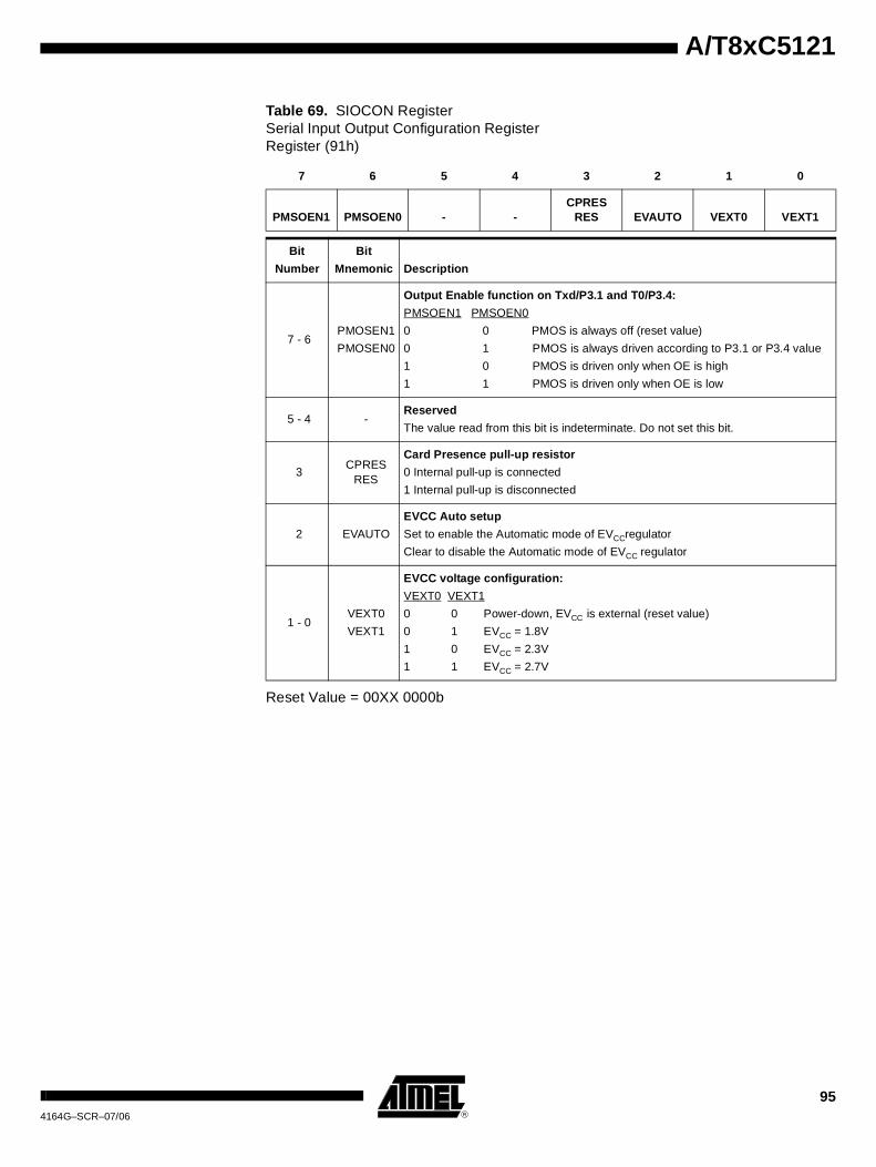
A/T8xC5121
Table 69. SIOCON RegisterSerial Input Output Configuration RegisterRegister (91h)
Reset Value = 00XX 0000b
7 6 5 4 3 2 1 0
PMSOEN1 PMSOEN0 - -CPRES
RES EVAUTO VEXT0 VEXT1
Bit
Number
Bit
Mnemonic Description
7 - 6PMOSEN1
PMOSEN0
Output Enable function on Txd/P3.1 and T0/P3.4:
PMSOEN1 PMSOEN0
0 0 PMOS is always off (reset value)
0 1 PMOS is always driven according to P3.1 or P3.4 value
1 0 PMOS is driven only when OE is high
1 1 PMOS is driven only when OE is low
5 - 4 -Reserved
The value read from this bit is indeterminate. Do not set this bit.
3CPRES
RES
Card Presence pull-up resistor
0 Internal pull-up is connected
1 Internal pull-up is disconnected
2 EVAUTO
EVCC Auto setup
Set to enable the Automatic mode of EVCCregulator
Clear to disable the Automatic mode of EVCC regulator
1 - 0VEXT0
VEXT1
EVCC voltage configuration:
VEXT0 VEXT1
0 0 Power-down, EVCC is external (reset value)
0 1 EVCC = 1.8V
1 0 EVCC = 2.3V
1 1 EVCC = 2.7V
954164G–SCR–07/06

Hardware Watchdog Timer
The WDT is intended as a recovery method in situations where the CPU may be sub-jected to software upset. The WDT consists of a 14-bit counter and the Watchdog TimerReSeT (WDTRST) SFR. The WDT is by default disabled from exiting reset. To enablethe WDT, user must write 01EH and 0E1H in sequence to the WDTRST, SFR location0A6H. When WDT is enabled, it will increment every machine cycle while the oscillatoris running and there is no way to disable the WDT except through reset (either hardwarereset or WDT overflow reset). When WDT overflows, it will drive an output RESET HIGHpulse at the RST-pin.
Using the WDT To enable the WDT, user must write 01EH and 0E1H in sequence to the WDTRST, SFRlocation 0A6H. When WDT is enabled, the user needs to service it by writing to 01EHand 0E1H to WDTRST to avoid WDT overflow. The 14-bit counter overflows when itreaches 16383 (3FFFH) and this will reset the device. When WDT is enabled, it willincrement every machine cycle while the oscillator is running. This means the user mustreset the WDT at least every 16383 machine cycle. To reset the WDT the user mustwrite 01EH and 0E1H to WDTRST. WDTRST is a write only register. The WDT countercannot be read or written. When WDT overflows, it will generate an output RESET pulseat the RST-pin. The RESET pulse duration is 96 x TCLK PERIPH, where TCLK PERIPH= 1/FCLK
PERIPH. To make the best use of the WDT, it should be serviced in those sections of codethat will periodically be executed within the time required to prevent a WDT reset.
To have a more powerful WDT, a 27 counter has been added to extend the Time-outcapability, ranking from 16 ms to 2s @ FOSCA = 12 MHz. To manage this feature, refer toWDTPRG register description, Table 70. The WDTPRG register should be configuredbefore the WDT activation sequence, and can not be modified until next reset.
Table 70. WDTRST Register
WDTRST - Watchdog Reset Register (0A6h)
Reset Value = XXXX XXXXb
Write only, this SFR is used to reset/enable the WDT by writing 01EH then 0E1H insequence.
7 6 5 4 3 2 1 0
- - - - - - - -
96 A/T8xC51214132C–SCR–07/06

A/T8xC5121
Table 71. WDTPRG Register
WDTPRG - Watchdog Timer Out Register (0A7h)
Reset Value = XXXX X000
WDT during Power-down and Idle
In Power-down mode the oscillator stops, which means the WDT also stops. While inPower-down mode the user does not need to service the WDT. There are 2 methods ofexiting Power-down mode: by a hardware reset or via a level activated external interruptwhich is enabled prior to entering Power-down mode. When Power-down is exited withhardware reset, servicing the WDT should occur as it normally should whenever theT8xC5121 is reset. Exiting Power-down with an interrupt is significantly different. Theinterrupt is held low long enough for the oscillator to stabilize. When the interrupt isbrought high, the interrupt is serviced. To prevent the WDT from resetting the devicewhile the interrupt pin is held low, the WDT is not started until the interrupt is pulled high.It is suggested that the WDT be reset during the interrupt service routine.
To ensure that the WDT does not overflow within a few states of exiting of powerdown, itis better to reset the WDT just before entering powerdown.
In the Idle mode, the oscillator continues to run. To prevent the WDT from resetting theT8xC5121 while in Idle mode, the user should always set up a timer that will periodicallyexit Idle, service the WDT, and re-enter Idle mode.
7 6 5 4 3 2 1 0
- - - - - S2 S1 S0
Bit
Number
Bit
Mnemonic Description
7 -
ReservedThe value read from this bit is undetermined. Do not try to set this bit.
6 -
5 -
4 -
3 -
2 S2 WDT Time-out select bit 2
1 S1 WDT Time-out select bit 1
0 S0 WDT Time-out select bit 0
S2 S1 S0 Selected Time-out0 0 0 (214 - 1) machine cycles, 16. 3 ms @ FOSCA =12 MHz0 0 1 (215 - 1) machine cycles, 32.7 ms @ FOSCA=12 MHz0 1 0 (216 - 1) machine cycles, 65. 5 ms @ FOSCA=12 MHz0 1 1 (217 - 1) machine cycles, 131 ms @ FOSCA=12 MHz1 0 0 (218 - 1) machine cycles, 262 ms @ FOSCA=12 MHz1 0 1 (219 - 1) machine cycles, 542 ms @ FOSCA=12 MHz1 1 0 (220 - 1) machine cycles, 1.05 ms @ FOSCA=12 MHz1 1 1 (221 - 1) machine cycles, 2.09 ms @ FOSCA=12 MHz
974132C–SCR–07/06

Electrical Characteristics
Absolute Maximum Ratings
DC Parameters TA = -40°C to +85°C; VSS = 0 V; VCC = 2.85V to 5.4V; F = 7.36 to 16 MHz
Table 72. Core DC Parameters (XTAL, RST, P0, P2, ALE, PSEN, EA)
Ambiant Temperature Under Bias ......................-25°C to 85°C
Storage Temperature ................................... -65°C to + 150°C
Voltage on VCC to VSS........................................-0.5V to + 6.0V
Voltage on Any Pin to VSS.......................... -0.5V to VCC + 0.5V
Note: Stresses at or above those listed under “ AbsoluteMaximum Ratings” may cause permanent damage tothe device. This is a stress rating only and functionaloperation of the device at these or any other condi-tions above those indicated in the operationalsections of this specification is not implied. Exposureto absolute maximum rating conditions may affectdevice reliability.
Symbol Parameter Min Typ Max Unit Test Conditions
VIL Input Low Voltage -0.5 0.2 VCC - 0.1 V
VIHInput High Voltage except XTAL1, RST
.2 VCC + .9 VCC + 0.5 V
VIH1Input High Voltage, XTAL1, RST
0.7 VCC VCC + 0.5 V
VOLOutput Low Voltage, Port 0 and 2
0.45 V IOL = 1.6 mA
VOHOutput High Voltage, Port 0 and 2
0.9 x VCC V IOH = -40 µA
DICCDigital Supply Output Current
6 10 mA CL = 100 nF
DVCCDigital Supply Voltage
2.5 2 .9 3.0 VCL = 100 nF
DIcc=10mA
IccNormal Power Down mode
80 100 µA 25°C
IccPulsed Power Down mode
20 30 µA 50°C Vcc=3V
Iccop Power Supply current
Iccop = 0.25 Freq (MHz) +4 mA
IccIDLE = 0.03 Freq (MHz) +5 mA
VCC = 5.4V and Bootloader execution
VPFDPPower-fail high level threshold
2 .55 V
VPFDMPower-fail low level threshold
2 .45 V
tGPower Fail glitch time
50 ns
trise, tfallVDD rise and fall time
1 μs 600 sec.
98 A/T8xC51214164G–SCR–07/06
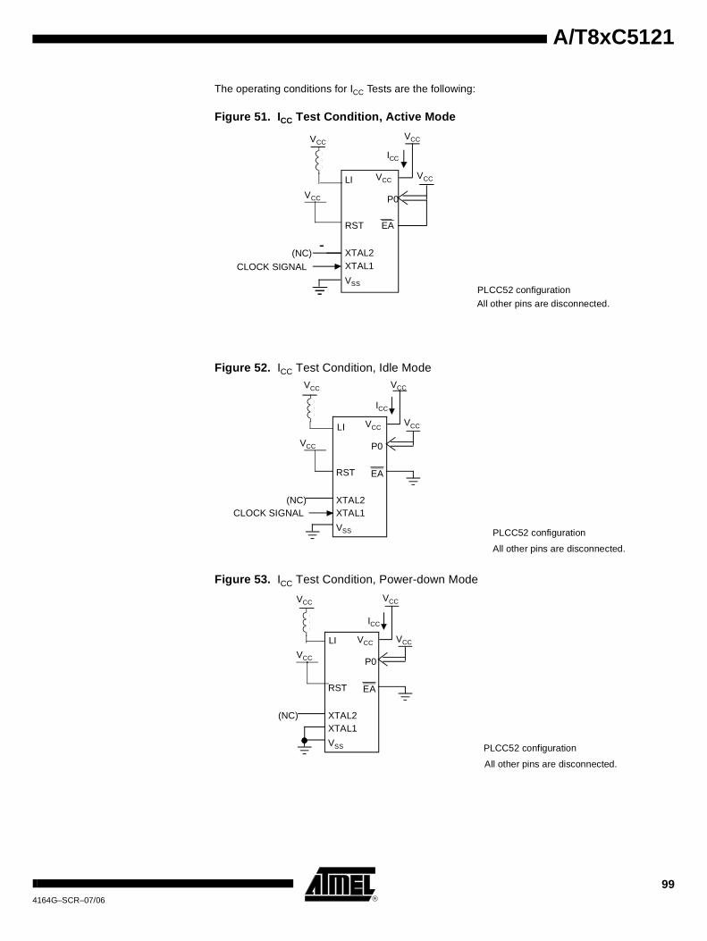
A/T8xC5121
The operating conditions for ICC Tests are the following:
Figure 51. ICC Test Condition, Active Mode
Figure 52. ICC Test Condition, Idle Mode
Figure 53. ICC Test Condition, Power-down Mode
EA
VCC
VCC
ICC
(NC)
CLOCK SIGNAL
All other pins are disconnected.
RST
XTAL2XTAL1
VSS
VCC
P0VCC
PLCC52 configuration
VCC
LI
RST EA
XTAL2XTAL1
VSS
VCC
VCC
ICC
(NC)
P0
VCC
All other pins are disconnected.
VCC
PLCC52 configuration
CLOCK SIGNAL
VCC
LI
RST EA
XTAL2XTAL1
VSS
VCC
VCC
ICC
(NC)
P0
VCC
All other pins are disconnected.
VCC
PLCC52 configuration
VCC
LI
994164G–SCR–07/06

Table 73. Serial Interface DC parameters (P3.0, P3.1, P3.3 and P3.4)
Table 74. LED outputs DC Parameters (P3.6 and P3.7)
Symbol Parameter Min Typ Max Unit Test Conditions
VIL Input Low Voltage
-0.5
-0.5
-0.5
0.4
0.5
0.5
V
V
V
EVCC = 1.8V
EVCC = 2.3V
EVCC = 2.8V
External EVcc
Automatic EVcc
VIH Input High Voltage
1.4
1.6
2.0
0.7 x EVCC EVCC
2.3
2.8
3.3
EVCC + 0.5
V
V
V
V
EVCC = 1.8V
EVCC = 2.3V
EVCC = 2.8V
External EVCC
Automatic EVcc
VOLOutput Low Voltage
0.4 V IOL = 1.2 mA
VOHOutput High Voltage
1.6
1.8
2.2
0.8 x EVCC
1.8
2.3
2.7
EVCC
V
V
V
V
EVCC = 1.8V IOH = 1 μA
EVCC = 2.3V
EVCC = 2.8V IOH = 10μA
External EVCC
EICCExtra Supply Current
+3 mA CL = 100 nF
EVCCExtra Supply Voltage
1.6
2.1
2.6
1.6
1.7
2.2
2.7
1.8
2.3
2.8
VCC
V
V
V
V
CL = 100 nF, 1.8V
CL = 100 nF, 2.3V
CL = 100 nF, 2.8V
External EVCC
Automatic EVcc
Ts Sampling time Automatic EVcc
Symbol Parameter Min Typ Max Unit Test Conditions
IOL
Output Low Current, P3.6 and P3.7 LED modes
1
2
5
2
4
10
4
8
20
mA
mA
mA
2 mA configuration
4 mA configuration
10 mA configuration
(TA = -20°C to +50°C, VCC - VOL = 2V ± 20%)
100 A/T8xC51214164G–SCR–07/06

A/T8xC5121
Table 75. Smart Card 5V Interface DC Parameters
Note: 1. Capacitor = 10 µF, X7R type. Maximum ESR value is 250 mohm, Inductor = 4.7 µH.
Table 76. Smart Card 3V Interface DC Parameters
Note: 1. Capacitor = 10 µF, X7R type. Maximum ESR value is 250 mohm, Inductor = 4.7 µH.
Table 77. Smart Card 1.8V Interface DC Parameters
Note: 1. Capacitor = 10 µF, X7R type. Maximum ESR value is 250 mohm, Inductor = 4.7 µH.
Symbol Parameter Min Typ Max Unit Test Conditions
CICCCard Supply Current
60
121
105
102
mA
VCC = 5.4V
VCC = 4V
VCC = 2.85V
CVCCCard Supply Voltage
4.6 5.4 V CIcc = 60 mA
CVCC Ripple on CVcc 200 mV 0<CIcc<60 mA
CVCC Spikes on CVcc 4.6 5.4 V
Maxi. charge 20 nA.s
Max. duration 400 ns
Max. variation CIcc 100 mA (1)
TVHLl CVcc to 0 750 μsCIcc = 0
CVcc = 5V to 0.4V (1)
Symbol Parameter Min Typ Max Unit Test Conditions
CICCCard Supply Current
60
110
89
110
mA
VCC = 5.4V
VCC = 4V
VCC = 2.85V
CVCCCard Supply Voltage
2.76 3.24 V CIcc = 60 mA
CVCC Ripple on CVcc 200 mV 0<CIcc<60 mA
CVCC Spikes on CVcc 2.76 3.24 V
Max. charge 10 ns
Max. duration 400 ns
Max. variation CIcc 50 mA
TVHLl CVcc to 0 750 μsCIcc = 0
CVcc = 5V to 0.4V (1)
Symbol Parameter Min Typ Max Unit Test Conditions
CICCCard Supply Current
20
109
100
82
mA
VCC = 5.4V
VCC = 4V
VCC = 2.85V
CVCCCard Supply Voltage
1.68 1.92 V CIcc = 20 mA
CVCC Spikes on CVcc 1.68 1.92 V
TVHLl CVcc to 0 750 μsCIcc = 0
CVcc = 5V to 0.4V (1)
1014164G–SCR–07/06

Table 78. Smart Card Clock DC Parameters (Port P1.4)
Note: 1. The voltage on CLK should remain between -0.3V and CVCC + 0.3V during dynamicoperation.
Table 79. Alternate Card Clock DC parameters (Port P3.6): 5V tolerant
Note: 1. The voltage on CLK should remain between -0.3V and VCC + 0.3V during dynamicoperation.
Symbol Parameter Min Typ Max Unit Test Conditions
VOLOutput Low Voltage
0(1)
0(1)
0.2 x CVCC
0.4
V IOL = 20 μΑ (1.8,3 V)
IOL = 50 μA (5V)
IOLOutput Low Current
15 mA
VOHOutput High Voltage
0.7 x CVCC
0.7 x CVCC
CVCC - 0.5
CVCC
CVCC
CVCC
V
V
V
IOH = 20 μA (1.8V)
IOH = 20 μA (3V)
IOH = 50 μA (5V)
IOHOutput High Current
15 mA
tR tF Rise and Fall time
16
22.5
50ns
CIN = 30 pF(5V)
CIN = 30 pF(3V)
CIN = 30 pF(1.8V)
Voltage Stability
-0.25
CVCC-0.5
0.4 x CVCC
CVCC + 0.25
V Low level
High level
Symbol Parameter Min Typ Max Unit Test Conditions
VOLOutput Low Voltage
0 (1)
0(1)0.2 x DVCC
0.5V IOL = 20 μA
IOL = -200 μA
VOHOutput High Voltage
0.7 x DVCC DVCC (1) V IOH = 20 μA
tR tFRise and Fall times
18 ns CIN = 30 pF
102 A/T8xC51214164G–SCR–07/06

A/T8xC5121
Table 80. Smart Card I/O DC Parameters (P1.0)
Note: 1. The voltage on RST should remain between -0.3V and CVCC + 0.3V during dynamicoperation.
Table 81. Alternate Card I/O DC Parameters (P3.5) : 5V tolerant
Note: 1. The voltage on I/O should remain between -0.3V and DVCC + 0.3V during dynamicoperation.
Symbol Parameter Min Typ Max Unit Test Conditions
VIL Input Low Voltage0(1)
0(1)
0.5
0.15 x CVCC
V IIL = 500 μA
IIL = 20 μA
IIL Input Low Current 500 μA
VIH Input High Voltage 0.7 x CVCC CVCC V IIH = -20 μA
IIH Input High Current -20 / +20 μA
VOLOutput Low Voltage
0(1)
0.4
0.4
0.3
V
IOL = 1μA (5V)
IOL = 1 mA (3V)
IOL = 1 mA (1.8V)
IOLOutput Low Current
15 mA
VOHOutput High Voltage
0.8 x CVCC CVCC (1) V IOH = 20 μA (5V,3V,1.8V)
IOHOutput High Current
15 mA
tR tFRise and Fall times
0.8 μs CIN = 30 pF Output
Symbol Parameter Min Typ Max Unit Test Conditions
VIL Input Low Voltage -0.3 0.2 x DVCC V IIL = 1 mA
VIH Input High Voltage 0.7 x DVCC DVCC + 0.3 V IIH = -20 μA
VOLOutput Low Voltage
0(1) 0.3 V IOL = 1000 μA
VOHOutput High Voltage
0.7 x DVCC DVCC (1) V IOH = 20 μA
tR tFRise and Fall delays
1 μs CIN = 30 pF
1034164G–SCR–07/06

Table 82. Smart Card RST, CC4, CC8, DC Parameters (Port P1.5, P1.3, P1.1)
Note: 1. The voltage on RST should remain between -0.3V and CVCC + 0.3V during dynamicoperation.
Table 83. Alternate Card RST DC Parameters (Port P3.7) : 5V tolerant
Note: 1. The voltage on RST should remain between -0.3V and DVCC + 0.3V during dynamicoperation.
Table 84. Card Presence DC Parameters (P1.2)
Symbol Parameter Min Typ Max Unit Test Conditions
VOL Output Low Voltage0(1)
0(1)
0.12 x CVCC
0.4V
IOL = 20 μΑ
IOL = 50 μΑ
IOL Output Low Current 15 mA
VOH Output High VoltageCVCC - 0.5
0.8 x CVCC
CVCC
CVCC (1)
V IOH = 50 μΑ
IOH = 20 μΑ
IOH Output High Current 15 mA
tR tF Rise and Fall delays 0.8 μs CIN = 30 pF
Voltage stability
-0.25
CVCC-0.5
0.4 x CVCC
CVCC + 0.25
Low level
High level
Symbol Parameter Min Typ Max Unit Test Conditions
VOL Output Low Voltage 0 (1) 0.2 x DVCC V IOL = 200 μΑ
VOH Output High Voltage0.8 x DVCC
0.8 x DVCC
DVCC (1)
DVCCV
IOH = 20 μΑ (1.8V)
IOH = 200 μΑ (3V)
tR tF Rise and Fall delays 400 μs CIN = 30 pF
Symbol Parameter Min Typ Max Unit Test Conditions
IOL1CPRES weak pull-up output current
3 10 25 μAP1.2 = 1, short to VSS
(internal pull-up enabled)
104 A/T8xC51214164G–SCR–07/06
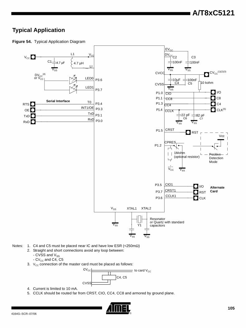
A/T8xC5121
Typical Application
Figure 54. Typical Application Diagram
Notes: 1. C4 and C5 must be placed near IC and have low ESR (<250mΩ)2. Straight and short connections avoid any loop between:
- CVSS and VSS- CVCC and C4, C5
3. VCC connection of the master card must be placed as follows:
4. Current is limited to 10 mA.5. CCLK should be routed far from CRST, CIO, CC4, CC8 and armored by ground plane.
10µF
VCC
RxD
TxD
VCC
TxD
RxD
XTAL1 XTAL2
LI
CPRES
CRST
CCLK
CC4
CC8
CIO
CVCC(1)(2)(3)
VSSI/O
C8
C4
CLK(5)
RST
4.7 µF
VSS
OE
RTS
VSS
VSS
INT1/OE
T0
VSS
100nF
VSS
DVCC
EVCC
100nF
VSS
DVCC(4)
LED0
LED1
C1C2 C3
C4
L1
4.7 µH
VSS VSS
Y1
I/O
RST
CLK
AlternateCard
CIO1
CRST1
CCLK1
VCC
1Mohm(optional resistor)
or VCC
Serial Interface
CVSS
22 pF
VSS
Vcc
PositiveDetectionMode
Resonatoror Quartz with standardcapacitors
100nFC5
C6
P1.2
P1.0
P1.1
P1.3
P1.4
P3.5
P3.7
P3.6
10 kohm
82 pF
VSS
C7
CVCC
P3.6
P3.7
P3.4
P3.3
P3.1
P3.0
P1.5
cVCC to card VCC
CVSS
C4, C5
1054164G–SCR–07/06

6. Distance between Device pads and Smart Card connector must be less than 4centimeters.
7. C6,C7 should be as close as possible to the Smart Card connector to reduce noiseand interferences.
106 A/T8xC51214164G–SCR–07/06
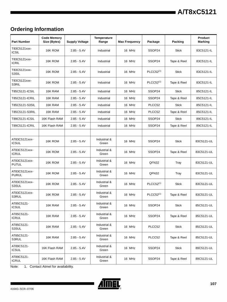
A/T8xC5121
Ordering Information
Note: 1. Contact Atmel for availability.
Part NumberCode Memory Size (Bytes) Supply Voltage
Temperature Range Max Frequency Package Packing
Product Marking
T83C5121xxx-ICSIL
16K ROM 2.85 - 5.4V Industrial 16 MHz SSOP24 Stick 83C5121-IL
T83C5121xxx-ICRIL
16K ROM 2.85 - 5.4V Industrial 16 MHz SSOP24 Tape & Reel 83C5121-IL
T83C5121xxx-S3SIL
16K ROM 2.85 - 5.4V Industrial 16 MHz PLCC52(1) Stick 83C5121-IL
T83C5121xxx-S3RIL
16K ROM 2.85 - 5.4V Industrial 16 MHz PLCC52(1) Tape & Reel 83C5121-IL
T85C5121-ICSIL 16K RAM 2.85 - 5.4V Industrial 16 MHz SSOP24 Stick 85C5121-IL
T85C5121-ICRIL 16K RAM 2.85 - 5.4V Industrial 16 MHz SSOP24 Tape & Reel 85C5121-IL
T85C5121-S3SIL 16K RAM 2.85 - 5.4V Industrial 16 MHz PLCC52 Stick 85C5121-IL
T85C5121-S3RIL 16K RAM 2.85 - 5.4V Industrial 16 MHz PLCC52 Tape & Reel 85C5121-IL
T89C5121-ICSIL 16K Flash RAM 2.85 - 5.4V Industrial 16 MHz SSOP24 Stick 89C5121-IL
T89C5121-ICRIL 16K Flash RAM 2.85 - 5.4V Industrial 16 MHz SSOP24 Tape & Reel 89C5121-IL
AT83C5121xxx-ICSUL
16K ROM 2.85 - 5.4VIndustrial &
Green16 MHz SSOP24 Stick 83C5121-UL
AT83C5121xxx-ICRUL
16K ROM 2.85 - 5.4VIndustrial &
Green16 MHz SSOP24 Tape & Reel 83C5121-UL
AT83C5121xxx-PUTUL
16K ROM 2.85 - 5.4VIndustrial &
Green16 MHz QFN32 Tray 83C5121-UL
AT83C5121xxx-PURUL
16K ROM 2.85 - 5.4VIndustrial &
Green16 MHz QFN32 Tray 83C5121-UL
AT83C5121xxx-S3SUL
16K ROM 2.85 - 5.4VIndustrial &
Green16 MHz PLCC52(1) Stick 83C5121-UL
AT83C5121xxx-S3RUL
16K ROM 2.85 - 5.4VIndustrial &
Green16 MHz PLCC52(1) Tape & Reel 83C5121-UL
AT85C5121-ICSUL
16K RAM 2.85 - 5.4VIndustrial &
Green16 MHz SSOP24 Stick 85C5121-UL
AT85C5121-ICRUL
16K RAM 2.85 - 5.4VIndustrial &
Green16 MHz SSOP24 Tape & Reel 85C5121-UL
AT85C5121-S3SUL
16K RAM 2.85 - 5.4VIndustrial &
Green16 MHz PLCC52 Stick 85C5121-UL
AT85C5121-S3RUL
16K RAM 2.85 - 5.4VIndustrial &
Green16 MHz PLCC52 Tape & Reel 85C5121-UL
AT89C5121-ICSUL
16K Flash RAM 2.85 - 5.4VIndustrial &
Green16 MHz SSOP24 Stick 89C5121-UL
AT89C5121-ICRUL
16K Flash RAM 2.85 - 5.4VIndustrial &
Green16 MHz SSOP24 Tape & Reel 89C5121-UL
1074164G–SCR–07/06

Package Drawings
SSOP24
108 A/T8xC51214164G–SCR–07/06

A/T8xC5121
PLCC52
1094164G–SCR–07/06

QFN32
110 A/T8xC51214164G–SCR–07/06

A/T8xC5121
Document Revision History for T8xC5121
Changes from 4164B -06/02 to 4164C - 07/03
1. Ports description update.
2. Added Bootloader Autobaud table.
3. Modified ICC test conditions Figure 51.
4. Added ICCOP power supply current characteristics.
5. Added ICCO pulsed power down mode current characteristics.
6. Modified Smart card characteristics : VCC/CVCC mixed.
Changes from 4164C - 07/03 to 4164D - 12/03
1. Changed value of EMV to EMV2000. Section “Features”, page 1.
Changes from 4164D - 12/03 to 4164E - 01/04
1. DVcc Min/Max values changed, page 96.
2. Alternate Card Pads are 5V tolerant, page 99.
Changes from 4164E - 01/04 to 4164F 11/05
1. Added green product ordering information.
Changes from 4164F 11/05 to 4164F 07/06
1. Added QFN32 package to ordering information.
1114164G–SCR–07/06

Table of Contents
Features ................................................................................................. 1
Description ............................................................................................ 2
Block Diagram ...................................................................................... 2
Pin Description ..................................................................................... 3Signals ...................................................................................................................5Port Structure Description....................................................................................10
SFR Mapping ....................................................................................... 12
PowerMonitor ...................................................................................... 14Description.......................................................................................................... 14PowerMonitor Diagram....................................................................................... 14
Power Monitoring and Clock Management ...................................... 16Idle Mode............................................................................................................ 16Power-down Mode.............................................................................................. 16
Clock Management............................................................................. 22Functional Block Diagram................................................................................... 22X2 Feature...........................................................................................................23Clock Prescaler....................................................................................................24Clock Control Registers ...................................................................................... 24
DC/DC Clock ....................................................................................... 27Clock Control Register........................................................................................ 27Clock Prescaler................................................................................................... 27
Smart Card Interface Block (SCIB) ................................................... 29Introduction ......................................................................................................... 29Main Features..................................................................................................... 29Block Diagram .....................................................................................................30Functional Description ........................................................................................ 30Other Features.....................................................................................................35DC/DC Converter.................................................................................................37Registers Description...........................................................................................38
Interrupt System ................................................................................. 47INT1 Interrupt Vector .......................................................................................... 48
LED Ports Configuration .................................................................... 57Registers Definition............................................................................................. 57
Dual Data Pointer ................................................................................ 58
i4164G–SCR–07/06
A/T8xC5121
A/T8xC5121
Memory Management ......................................................................... 60Program Memory................................................................................................ 60In-System Programming..................................................................................... 63Protection Mechanisms ...................................................................................... 66Autobaud ............................................................................................................ 71Protection Mechanisms ...................................................................................... 71
Timers/Counters ................................................................................. 73Introduction ......................................................................................................... 73Timer 0/Counter Operations ............................................................................... 73Timer 0.................................................................................................................74Timer 1.................................................................................................................77Registers............................................................................................................. 78
Serial I/O Port ...................................................................................... 81Framing Error Detection ..................................................................................... 81Automatic Address Recognition.......................................................................... 82UART Output Configuration................................................................................ 84UART Control Registers ..................................................................................... 85
UART Timings ..................................................................................... 86Mode Selection................................................................................................... 86Baud Rate Generator.......................................................................................... 86Asynchronous Modes (Modes 1, 2 and 3) ...........................................................89
Hardware Watchdog Timer ................................................................ 96Using the WDT ................................................................................................... 96WDT during Power-down and Idle...................................................................... 97
Electrical Characteristics ................................................................... 98Absolute Maximum Ratings ............................................................................... 98DC Parameters................................................................................................... 98
Typical Application ........................................................................... 105
Ordering Information........................................................................ 107
Package Drawings............................................................................ 108SSOP24............................................................................................................ 108PLCC52 .............................................................................................................109QFN32 ...............................................................................................................110
Document Revision History for T8xC5121 ..................................... 111Changes from 4164B -06/02 to 4164C - 07/03................................................. 111Changes from 4164C - 07/03 to 4164D - 12/03................................................ 111Changes from 4164D - 12/03 to 4164E - 01/04................................................ 111
ii4164G–SCR–07/06

Changes from 4164E - 01/04 to 4164F 11/05 .................................................. 111Changes from 4164F 11/05 to 4164F 07/06..................................................... 111
Table of Contents .................................................................................. i
4164G–SCR–07/06
iii A/T8xC5121

© Atmel Corporation 2006. All rights reserved. Atmel®, logo and combinations thereof, are registered trademarks, and Everywhere You Are®
are the trademarks of Atmel Corporation or its subsidiaries. Other terms and product names may be trademarks of others.
Disclaimer: The information in this document is provided in connection with Atmel products. No license, express or implied, by estoppel or otherwise,to anyintellectu-alproperty right is granted by this document or in connection with the sale of Atmel products. EXCEPT AS SET FORTH IN ATMEL’S TERMS AND CONDI-TIONS OFSALE LOCATED ON ATMEL’S WEB SITE, ATMEL ASSUMES NO LIABILITY WHATSOEVER AND DISCLAIMS ANY EXPRESS, IMPLIED OR STATUTORYWAR-RANTY RELATING TO ITS PRODUCTS INCLUDING, BUT NOT LIMITED TO, THE IMPLIED WARRANTY OF MERCHANTABILITY, FITNESS FOR A PARTICU-LARPURPOSE, OR NON-INFRINGEMENT. IN NO EVENT SHALL ATMEL BE LIABLE FOR ANY DIRECT, INDIRECT, CONSEQUENTIAL, PUNITIVE, SPECIALOR INCIDEN-TAL DAMAGES (INCLUDING, WITHOUT LIMITATION, DAMAGES FOR LOSS OF PROFITS, BUSINESS INTERRUPTION, OR LOSS OF INFORMA-TION) ARISING OUTOF THE USE OR INABILITY TO USE THIS DOCUMENT, EVEN IF ATMEL HAS BEEN ADVISED OF THE POSSIBILITY OF SUCH DAM-AGES. Atmel makes norepresentationsor warranties with respect to the accuracy or completeness of the contents of this document and reserves the right to makechanges to specificationsand product descriptions at any time without notice. Atmel does not make any commitment to update the information contained herein.Unless specifically provided otherwise, Atmel products are not suitable for, and shall not be used in, automotive applications. Atmel’s products are not intended,authorized, or warranted for useas components in applications intended to support or sustainlife.
Atmel Corporation Atmel Operations
2325 Orchard ParkwaySan Jose, CA 95131, USATel: 1(408) 441-0311Fax: 1(408) 487-2600
Regional Headquarters
EuropeAtmel SarlRoute des Arsenaux 41Case Postale 80CH-1705 FribourgSwitzerlandTel: (41) 26-426-5555Fax: (41) 26-426-5500
AsiaRoom 1219Chinachem Golden Plaza77 Mody Road TsimshatsuiEast KowloonHong KongTel: (852) 2721-9778Fax: (852) 2722-1369
Japan9F, Tonetsu Shinkawa Bldg.1-24-8 ShinkawaChuo-ku, Tokyo 104-0033JapanTel: (81) 3-3523-3551Fax: (81) 3-3523-7581
Memory2325 Orchard ParkwaySan Jose, CA 95131, USATel: 1(408) 441-0311Fax: 1(408) 436-4314
Microcontrollers2325 Orchard ParkwaySan Jose, CA 95131, USATel: 1(408) 441-0311Fax: 1(408) 436-4314
La ChantrerieBP 7060244306 Nantes Cedex 3, FranceTel: (33) 2-40-18-18-18Fax: (33) 2-40-18-19-60
ASIC/ASSP/Smart CardsZone Industrielle13106 Rousset Cedex, FranceTel: (33) 4-42-53-60-00Fax: (33) 4-42-53-60-01
1150 East Cheyenne Mtn. Blvd.Colorado Springs, CO 80906, USATel: 1(719) 576-3300Fax: 1(719) 540-1759
Scottish Enterprise Technology ParkMaxwell BuildingEast Kilbride G75 0QR, Scotland Tel: (44) 1355-803-000Fax: (44) 1355-242-743
RF/AutomotiveTheresienstrasse 2Postfach 353574025 Heilbronn, GermanyTel: (49) 71-31-67-0Fax: (49) 71-31-67-2340
1150 East Cheyenne Mtn. Blvd.Colorado Springs, CO 80906, USATel: 1(719) 576-3300Fax: 1(719) 540-1759
Biometrics/Imaging/Hi-Rel MPU/High Speed Converters/RF Datacom
Avenue de RochepleineBP 12338521 Saint-Egreve Cedex, FranceTel: (33) 4-76-58-30-00Fax: (33) 4-76-58-34-80
Literature Requestswww.atmel.com/literature
Printed on recycled paper.
4164G–SCR–07/06