t. rao, j. - brookhaven national laboratory · i. ben-zvi,x. chang, j. keister, e. muller, t. rao,...
TRANSCRIPT
Pres. PAC'09 Conf., Vancouver, BC4-8 May (2009)
BNL 90604-2009-CP
INVESTIGATION OF CHARGE GAIN IN DIAMOND ELECTRONBEAM AMPLIFIERS VIA 3D SIMULATIONS*
R. Busby, D.A. Dimitrov, and J.R. CaryTech-X CorporationBoulder, CO 80303
I. Ben-Zvi, X. Chang, J. Keister, E. Muller, T. Rao, J. Smedley, and Q. WuBrookhaven National Laboratory
Upton, NY 11973-5000
May,2009
*This manuscript has been authored by Brookhaven Science Associates, LLC underContract No. DC-AC02-98CHI0886 with the U.S. Department of Energy. The UnitedStates Government retains, and the publisher, by accepting the article for publication,acknowledges, a world-wide license to publish or reproduce the published form of thismanuscript, or allow others to do so, for the United States Government purposes.

DISCLAIMER
This work was prepared as an account of work sponsored by an agency of the UnitedStates Government. Neither the United States Government nor any agency thereof, norany of their employees, nor any of their contractors, subcontractors, or their employees,makes any warranty, express or implied, or assumes any legal liability or responsibilityfor the accuracy, completeness, or any third party's use or the results of such use of anyinformation, apparatus, product, or process disclosed, or represents that its use wouldnot infringe privately owned rights. Reference herein to any specific commercialproduct, process, or service by trade name, trademark, manufacturer, or otherwise, doesnot necessarily constitute or imply its endorsement, recommendation, or favoring by theUnited States Government or any agency thereof or its contractors or subcontractors.The views and opinions of authors expressed herein do not necessarily state or reflectthose ofthe United States Government or any agency thereof.
.~
INVESTIGATION OF CHARGE GAIN IN DIAMOND ELECTRON BEAMAMPLIFIERS VIA 3D SIMULATIONS*
D. A. Dimitrov, R. Busby, J. R. Cary, Tech-X Corp., Boulder, CO 80303, USAI. Ben-Zvi, X. Chang, J. Keister, E. Muller, T. Rao, J. Smedley, Q. Wu, BNL, Upton, NY 11973, USA
Abstract
A promising new concept of a diamond amplified photocathode for generation of high-current, high-brightness,and low thermal emittance electron beams was recentlyproposed [1] and is currently under active development. Tobetter understand the different effects involved in the generation ofelectron beams from diamond, we have been developing models (within the VORPAL computational framework) to simulate secondary electron generation and chargetransport. The currently implemented models include inelastic scattering of electrons and holes for generation ofelectron-hole pairs, elastic, phonon, and charge impurityscattering. We will present results from 3D VORPAL simulations with these capabilities on charge gain as a function of primary electron energy and applied electric field.Moreover, we consider effects of electron and hole cloudexpansion (initiated by primary electrons) and separationin a surface domain of diamond.
INTRODUCTION
To address the need for high average-current, highbrightness electron beams in current and future acceleratorbased systems (e.g. electron cooling of hadron accelerators, energy-recovery linac light sources, and ultra-highpower free electron lasers), a new design for a photoinjector with a diamond amplifier was proposed [1] and is underactive development [2].
This new photoinjector concept has important advantages [1] compared to existing metallic and semi-conductorphotocathodes. The idea of its operation is to first generate a primary electron beam using a conventional photocathode and inject it into diamond. The primary electronsscatter in the diamond, generating a cascade of secondaryelectrons. More recently, highly energetic photons are alsobeing considered in experiments as a source for generationof secondary electrons in diamond instead ofusing a beamofprimary electrons. The secondary electrons drift throughthe diamond under the acceleration of an applied electricfield. The transported, large number of secondary electrons(compared to the number of primaries) are emitted from adiamond surface with a negative electron affinity (NEA)into the accelerating cavity of an electron gun.
We have been implementing models [4] (and our otherpaper in this proceedings), within the VORPAL [3] computational framework, for simulation of secondary electron
* We are grateful to the US DoE for supporting this work under theDE-FG02-06ER84509 grant.
generation and charge transport in diamond in order to better understand the phenomena involved in electron amplification and emission from diamond. Here, we report results on gain when we consider only the loss of electronsdue to the electron cloud expansion near the diamond surface where primary electrons enter. Moreover, we compare simulation results with results from experiments [2]on electron gain when using primary electrons to generatethe secondaries.
SIMULATION MODELS
When a primary electron with sufficiently high energyenters into diamond, it can experience inelastic scatteringleading to losing part of its energy to create electron-hole(e-h) pairs. Moreover, some of the secondary electrons andthe related holes are created with large enough energies toalso undergo such inelastic scattering and create additionale-h pairs.
Generally, these inelastic processes continue until thefree charge carriers (electrons in the conduction band andholes in valance band) in diamond no longer have enoughenergy to cause the transition of electrons from the valanceto the conduction band. The minimum energy for suchtransitions is equal to the energy gap in diamond, EG ==5.46 eV at room temperature. However, the mean free timebetween such inelastic scattering events (it can be obtainfrom the total cross section for this process [5,4]) increasestowards infinity when the energy of the charge carrier decreases towards EG. Effectively, when the energy of thefree carriers is close to 10 eV, the further relaxation of theelectrons towards the bottom of the conduction band andthe holes towards the top of the valance band is due to lowenergy inelastic scattering with phonons.
For the results presented here, we used our implementation of the Ashley's model [5] (and the references therein)for the inelastic scattering for secondary electron generation at 300 K (this extends our initial implementation ofthis model [4] to T > 0 K). For the low-energy inelastic scattering with optical and acoustic phonons we implemented Monte Carlo algorithms based on the models givenby Jacoboni and Reggiani [6]. We have validated that theelectron-phonon scattering implementation leads to electron drift velocities that agree well with band structure calculations and with experimental data [7].
From the time a primary electron enters diamond, thesecondary electron generation is close to complete after200 fs. The code switches electrons and holes to phononscattering only, once their energy falls below 11 eV during
1000
1.0 1.5 2.0x (pm)
100
0.5 1.0 1.5 2.0x (pm)
1.0"..---,...--r-==="
: ··eleetzoou~ .......
: : : :
0.5 ~.~~ ·.:~J · ·.~~ ···_· ·t """"" · ·j"- " ·" " · "
! 0.0 ~ ~.L ~ ..~ : ' .
-0.5 ! ~t.: .\.l .- .: L85~
2.0
0.1 1 10time (ps)
..~ :: ....
: u~
0.5 1.0 1.5x (pm)
180 .---~--...,--"'p:;::::~~~~C!b160
rIJ 140..a 120
l 100~ 80'S 60=-= 40
20
8.01
: •• e1ect:roa.~ . , ..1_
-1.0 0.0 0.5 1.0 1.5
x (pm)
-0.5 ; ; ~ -I
0.5 t~" 'i<" :\:~ ( : _.._..-i \3- 0.0 ~~~ ..< ; .
~ ~:::~: .•.•: i'-0.6 ~ · ..:··· · · · · · · ~· · .· ·· · ..····i···..········t····_·..···-
i3- 0.0.-1lI...,~· , ·· :..· ·~
~ ' .~
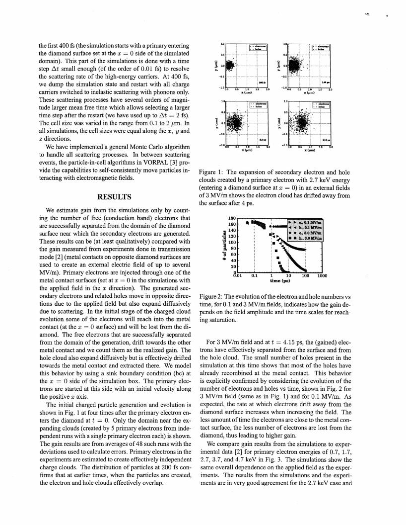
For 3 MY/m field and at t == 4.15 ps, the (gained) electrons have effectively separated from the surface and fromthe hole cloud. The small number of holes present in thesimulation at this time shows that most of the holes havealready recombined at the metal contact. This behavioris explicitly confirmed by considering the evolution of thenumber of electrons and holes vs time, shown in Fig. 2 for3 MY/m field (same as in Fig. 1) and for 0.1 MV/m. Asexpected, the rate at which electrons drift away from thediamond surface increases when increasing the field. Theless amount oftime the electrons are close to the metal contact surface, the less number of electrons are lost from thediamond, thus leading to higher gain.
We compare gain results from the simulations to experimental data [2] for primary electron energies of 0.7, 1.7,2.7,3.7, and 4.7 keY in Fig. 3. The simulations show thesame overall dependence on the applied field as the experiments. The results from the simulations and the experiments are in very good agreement for the 2.7 keV case and
Figure 2: The evolution ofthe electron and hole numbers vstime, for 0.1 and 3 MY/m fields, indicates how the gain depends on the field amplitude and the time scales for reaching saturation.
Figure 1: The expansion of secondary electron and holeclouds created by a primary electron with 2.7 keY energy(entering a diamond surface at x == 0) in an external fieldsof 3 MV/m shows the electron cloud has drifted away fromthe surface after 4 pSt
RESULTS
the first 400 fs (the simulation starts with a primary enteringthe diamond surface set at the x == 0 side of the simulateddomain). This part of the simulations is done with a timestep tlt small enough (of the order of 0.01 fs) to resolvethe scattering rate of the high-energy carriers. At 400 fs,we dump the simulation state and restart with all chargecarriers switched to inelastic scattering with phonons only.These scattering processes have several orders of magnitude larger mean free time which allows.selecting a largertime step after the restart (we have used up to tlt == 2 fs).The cell size was varied in the range from 0.1 to 2 usn. Inall simulations, the cell sizes were equal along the x, y andz directions.
We have implemented a general Monte Carlo algorithmto handle all scattering processes. In between scatteringevents, the particle-in-cell algorithms in VORPAL [3] provide the capabilities to self-consistently move particles interacting with electromagnetic fields.
We estimate gain from the simulations only by counting the number of free (conduction band) ' electrons thatare successfully separated from the domain of the diamondsurface near which the secondary electrons are generated.These results can be (at least qualitatively) compared withthe gain measured from experiments done in transmissionmode [2] (metal contacts on opposite diamond surfaces areused to create an external electric field of up to severalMY/m). Primary electrons are injected through one of themetal contact surfaces (set at x == 0 in the simulations withthe applied field in the x direction). The generated secondary electrons and related holes move in opposite directions due to the applied field but also expand diffusivelydue to scattering. In the initial stage of the charged cloudevolution some of the electrons will reach into the metalcontact (at the x == 0 surface) and will be lost from the diamond. The free electrons that are successfully separatedfrom the domain of the generation, drift towards the othermetal contact and we count them as the realized gain. Thehole cloud also expand diffusively but is effectively driftedtowards the metal contact and extracted there. We modelthis behavior by using a sink boundary condition (be) atthe x == 0 side of the simulation box. The primary electrons are started at this side with an initial velocity alongthe positive x axis.
The initial charged particle generation and evolution isshown in Fig. 1 at four times after the primary electron enters the diamond atz == O. Only the domain near the expanding clouds (created by 5 primary electrons from independent runs with a single primary electron each) is shown.The gain results are from averages of48 such runs with thedeviations used to calculate errors. Primary electrons in theexperiments are estimated to create effectively independentcharge clouds. The distribution of particles at 200 fs confirms that at earlier times, when the particles are created,the electron and hole clouds effectively overlap.

are close at the lower energies. However, for the 3.7 and4.7 keV cases, the simulations predict 16 and 25 % highergain than observed in the experiments.
to generate an electron-hole pair. This value is within therange from 10 to 17 eV reported [5] previously by differentexperimental, theoretical, and computational studies.
SUMMARY
We reported here initial simulation results on charge gainfrom diamond that indicate the gain can be optimized byincreasing the primary electron energy and the magnitudeof the applied electric field. However, increasing the fieldwill lead to increasing the effective temperature ofthe drifting electrons (the regime of hot electron transport) potentially increasing the thermal emittance ofthe emitted beam.At the intermediate primary electron energies considered,the gain from the simulations agrees very well with experimental data. At the higher energies, the simulations predictlarger gain than the experiments. However, in the simulations we have considered only loss due to the diffusive motion near the diamond surface where secondary electronsare generated. In the future, we will investigate the complete transmission process, including effects of trappingand collection of the electrons at the second metal contact.We are also implementing a more accurate model for thesecondary electron generation and will consider emissionfrom diamond with different electron affinities. Finally, wehave started to investigate via simulations secondary electron generation caused by highly energetic photons to better understand results from such experiments.
...... ...,: ~ ~ : ; :. .... ,. ~ ..· . . . . . . .· . . . . . . .· .. . .. "· . . . . . . ... ..._ _ .: ::: : :: : : : I • : :
..... ..-:- :- ~ :. ....! :- : ~ " ...· .. .• • I • • I • •I • • • • • • •
... .. .: : ·· ·· :..· · · ··i ..· ..·· ..:· · .._..· :· · · · · · ·:· · · · ·I • • • I I
• •• • I •· .. ""........ ~. • .. .. r ~ : ; : ~ ~" .
: : : : : : :. . . . . . .
.. "... " ... .. .. .. .:" ;- ~ : i -: :. .. .. .. .. .. -· . . . . . . .
• • • • I • • •· . . . . . . .
350 ..-........--r"-~...,.......,.-.,..... ............,.----.
~ 300
.~ 250
: 200
i 150G)
'i 100
~ 50
350 ,---..,.---T"""----r--,.--..,.--.....
lb.5 1.0 1.5 2.0 2.5 3.0 3.5 4.0 4.5 5.0Primary electron energy (keY>
Figure 3: Comparison of the electron gain from transmission experiments [2] with the simulations shows the samebehavior for different primary electron energies and fields.
Figure 4: The maximum number of electrons in the driftedclouds indicates two orders of magnitude charge gain forprimary electron energy larger than 2.5 keY.
The higher gain seen in the simulations for these twocases could potentially be due to two reasons. In the simulations, the gain was determined by the number ofelectronsthat are successfully separated from the metal contacs atdiamond surface near which the generation happens. Anyadditional electron loss during the propagation to the othermetal contact is not taken into account (e.g., due to trapping or recombination with holes in diamond). However,the gain from the experiments is determined by the totaltransmitted charge collected at the opposite metal contact.Secondly, the gain in the experiments was determined [2]assuming that the primary electrons lose a constant amountof energy when going through the metal contacts beforeentering in diamond. However, this loss is generally dependent on the energy of the particles.
The dependence of the maximum gain on the primaryelectron energy in the simulations, shown in Fig. 4, indicates that at higher energies, the diffusive motion doesnot affect the gain as much as at lower energies. For a 4.7keV primary electron, the average energy to generate a secondary electrons is about 15 eV,while for a 700 eV primaryelectron, it is 38 eV. Note that simulations started with aprimary electron in bulk diamond using with this model forthe inelastic scattering show about 14 eV average energy
REFERENCES
[1] I. Ben-Zvi, X. Chang, P. D. Johnson, 1. Kewisch, and T. Rao.Secondary emission enhanced photoinjector. C-AD Accelerator Physics Report C-A/AP/149, BNL, 2004.
[2] X. Chang, I. Ben-Zvi, A. Burrill, J. Grimes, T. Rao,Z. Segalov, 1. Smedley, Q. WU Recent Progress on theDiamond Amplified Photo-cathode Experiment. In PAC07,IEEE, pp. 2044-6, 2007; X. Chang et al., First Observation ofan Electron Beam Emitted from a Diamond Amplified Cathode. In these proceedings.
[3] C. Nieter and 1. R. Cary. VORPAL: a versatile plasma simulation code. J. Comput. Phys., 196:448-473,2004.
[4] D. A. Dimitrov, R. Busby, D. L. Bruhwiler, J. R. Cary, I. BenZvi, T. Rao, X. Chang, 1. Smedley, Q. Wu 3D Simulations ofSecondary Electron Generation and Transport in a DiamondAmplifier for Photocathodes In PAC07, IEEE, pp. 3555-7,2007.
[5] B. Ziaja, R. A. London, and J. Hajdu. Unified model ofsecondary electron cascades in diamond. J. Appl. Phys.,97:064905-1/9, 2005.
[6] C. Jacoboni and L. Reggiani The Monte Carlo method forthe solution of charge transport in semiconductors with applications to covalent materials Rev. Mod. Phys., 64:645-705,1983.
[7] T. Watanabe, T. Teraji, T. Ito, Y. Kamakura, and K. TaniguchiMonte Carlo simulations of electron transport properties ofdiamond in high electric fields using full band structure J.Appl. Phys. 95:4866-74, 2004.