systems for petascale...
TRANSCRIPT

Integrated Micro and Nano Photonic Systems for Petascale Networking
Prof. S. J. Ben Yoo, UC Davis Campus CITRIS Director [email protected]
http://sierra.ece.ucdavis.edu http://citris.ucdavis.edu Tokyo, Japan April 10, 2006

2
OUTLINE
§Optical LabelSwitching Routers §Optical CDMA §Optical Arbitrary Waveform Generators §Photonic Interconnect Nano Processors

3
Sensor Network
Storage Area Network
Core Router IPNE
DATA
LABEL
Legacy IP Network
Wireline MPLS IPNE
DATA
LABEL
Optical Label Switching Network
Wireline OCDMA LAN
Satellite Network
Reconfigurable Wireless Network
Next Generation Heterogeneous Networking

4 Client networks Client networks
AllOptical Label Switching Router Systems Integration at UC Davis
AllOptical Label Switching Router Systems Integration at UC Davis
fiber delay
Label reader
DEM
UX
NC&M
Switching Fabric
Label Processing ModuleTI (LPTI)
OLS Edge Router
CI CI CI
OLE OLR OLE OLR OLE OLR
IP Router ATM Client Machine
500 psec/div
500 psec/div UNAS
...
Switch Controller w/ Forwarding Lookup Table
5
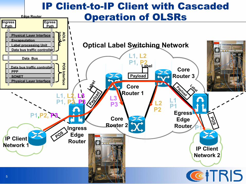
IP ClienttoIP Client with Cascaded Operation of OLSRs
IP Client Network 1
Optical Label Switching Network
Core Router 3
Ingress Edge Router
POS
Payload
Label
POS
IP Client Network 2
Egress Edge Router
Core Router 2
Core Router 1
Payload
Label
Payload
Label
P1,P2, P3
P3
P1, P2
P2 P1 L1
L1, L2
L2 L3 P1, P2, P3
L1, L2, L3
P1
Physical Layer Interface Encapsulation Label processing Unit Data bus traffic controller
Data Bus
SONET PPP
Physical Layer Interface
Data bus traffic controller
AOLS
Interface PO
S Interface
Ingress Path
Egress Path
Edge Router
6
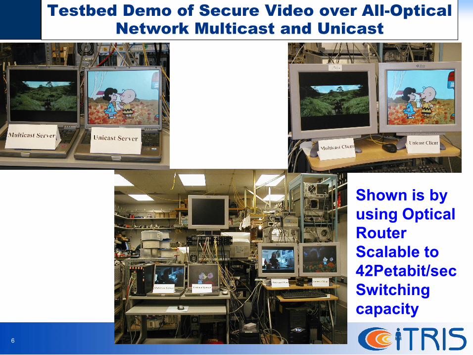
Testbed Demo of Secure Video over AllOptical Network Multicast and Unicast
Shown is by using Optical Router Scalable to 42Petabit/sec Switching capacity

7
Sprint ATL
LLNL
477 km Optical Label Switching Field Trial (OFC2002, #TuY4)
V.J. Hernandez, et al, "First Field Trial of Optical Label Switching and Packet Dropping on a 477km NTON/Sprint Link,"
477 km Optical Label Switching Field Trial (OFC2002, #TuY4)
V.J. Hernandez, et al, "First Field Trial of Optical Label Switching and Packet Dropping on a 477km NTON/Sprint Link,"

8
Slow w
aveguide
Norm
al waveguide
All Optical Variable Buffers: Nano Photonic Crystals for Slow Light
Pipelined Wavelength, Time, and Space Domain Contention Resolution

9
ChipScale Optical Router Microsystem
S. J. B. Yoo, “UltraLow Latency MultiProtocol Optical Routers for the Next Generation Internet,” U. S. Patent 6,925,257 B2 (2005). S. J. B. Yoo, “Integrated Optical Router,” U. S. Patent 6,768,827 (2004). S. J. B. Yoo, “UltraLow Latency MultiProtocol Optical Routers for the Next Generation Internet,” U. S. Patent 6,519,062 (2000). S. J. B. Yoo, “Wavelength Converter with Modulated Absorber,” U. S. Patent 6,563,627 (2001). S. J. B. Yoo, “Compact Optical Receiver with Optical Signal Processing Capabilities,” U. S. Patent pending (2001). S. J. B. Yoo, G. K. Chang, “HighThroughput, LowLatency Next Generation Internet Using Optical Tag Switching,” U. S. Patent 6,111,673.(1997)
10
Buffer Memory Buffer Memory Buffer Memory M
AC
Buffer Memory M
AC
Buffer Memory Buffer Memory Buffer Memory M
AC
Buffer Memory M
AC Buffer
Memory Buffer Memory M
AC
Buffer Memory M
AC
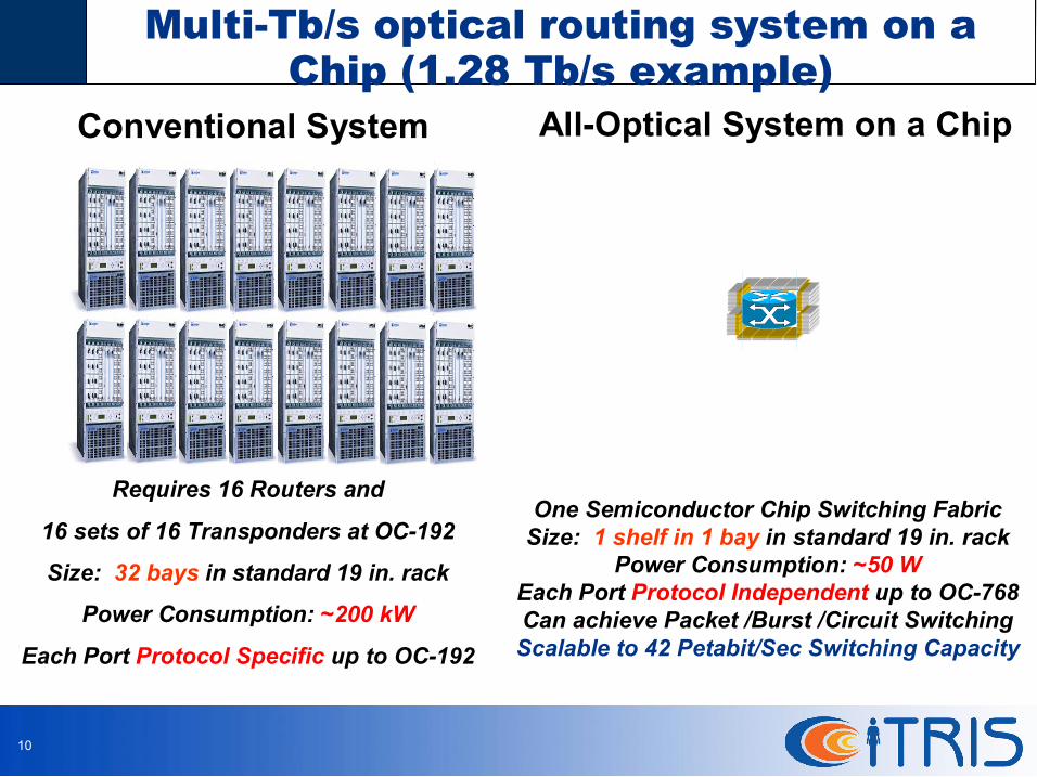
Requires 16 Routers and
16 sets of 16 Transponders at OC192
Size: 32 bays in standard 19 in. rack
Power Consumption: ~200 kW
Each Port Protocol Specific up to OC192
One Semiconductor Chip Switching Fabric Size: 1 shelf in 1 bay in standard 19 in. rack
Power Consumption: ~50 W Each Port Protocol Independent up to OC768 Can achieve Packet /Burst /Circuit Switching Scalable to 42 Petabit/Sec Switching Capacity
Conventional System AllOptical System on a Chip MAC
MAC
MultiTb/s optical routing system on a Chip (1.28 Tb/s example)

11
OUTLINE
§Optical LabelSwitching Routers §Optical CDMA §Optical Arbitrary Waveform Generators §Photonic Interconnect Nano Processors
Higher Capacity Networking (~ 1 Tb/s LAN) More flexible bandwidth assignment Higher Level of Security

12
Optical CDMA Technology
Substrate Array Waveguides
Input Waveguide Output Waveguide
modulators
Substrate Array Waveguides
Input Waveguide Output Waveguide
modulators
INPUT PULSE
Encoded PULSE
OUTPUT PULSE
Grating Grating
Lens Lens SLPM
Input Output
Phase
Grating
Lens Lens SLPM
Input Output
Phase
WeinerHeritage ’85; Heritage Tutorial OFC 2006 OThT1
J. Cao et al OFC 2006 OWL2

13
OCDMA Testbed Cong et al OFC 2006 OThT5

14
4 Users 8 Users 16 Users 32 Users 16 Users 32 Users 8 Users 4 Users
320 Gb/s OCDMA Network Testbed Demonstration
Without FEC With FEC V. J. Hernandez, W. Cong, R. P. Scott, C. Yang, N. K. Fontaine, B. H. Kolner, J. P. Heritage, S. J. B. Yoo, "320Gb/s capacity (32 users x 10 Gb/s) SPECTS OCDMA local area network testbed," postdeadline paper OFC'06, Mar. 2006.
15
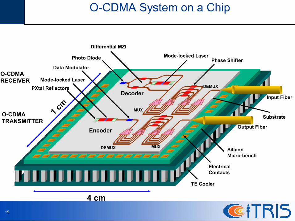
DEMUX
Substrate
Modelocked Laser
TE Cooler
Silicon Microbench
Output Fiber
Input Fiber
Electrical Contacts
Modelocked Laser
Differential MZI
Photo Diode
OCDMA TRANSMITTER
OCDMA RECEIVER
Data Modulator
Encoder
MUX DEMUX
MUX
Phase Shifter
Decoder
4 cm
1 cm
PXtal Reflectors
OCDMA System on a Chip

16
OCDMA
Encoder/
decoder
Differential
MachZehnder
FP Absorber
waveguide
Colliding
Pulse
Modelocked
Laser
OCDMA Microsystem Integration
17
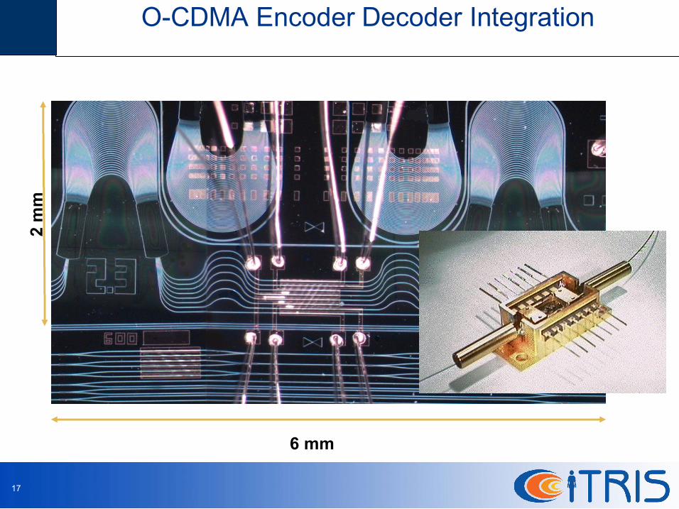
6 mm
2 mm
OCDMA Encoder Decoder Integration

18
Substrate Array Waveguides
Input Waveguide Output Waveguide
modulators
INPUT PULSE
Encoded PULSE
OUTPUT PULSE
W5 encoding
10 0 10
0.00
0.02
0.04
0.06
0.08
0.10
0.12
0.14 Experimental result Simulation
SHG (m
V)
Time (ps)
W5 en; W5* decoding
10 0 10 0.00
0.02
0.04
0.06
0.08
0.10
0.12
0.14 Experimental result Simulation
SHG (m
V)
Time (ps)
W5 en; W6 * decoding
10 0 10 0.00
0.02
0.04
0.06
0.08
0.10
0.12
0.14 Experimental result Simulation
SHG (m
V)
Time (ps)
Pulse without coding
10 0 10 0.00
0.02
0.04
0.06
0.08
0.10
0.12
0.14 Experimental result Simulation
SHG (m
V)
Time (ps)
InP OCDMA Microsystem Encoding/Decoding Experiments

19
26mm
13m
m
8x200
16x100
32x50
64x25
8, 16, 32, and 64 ch InP OCDMA Encoder/Decoders
20
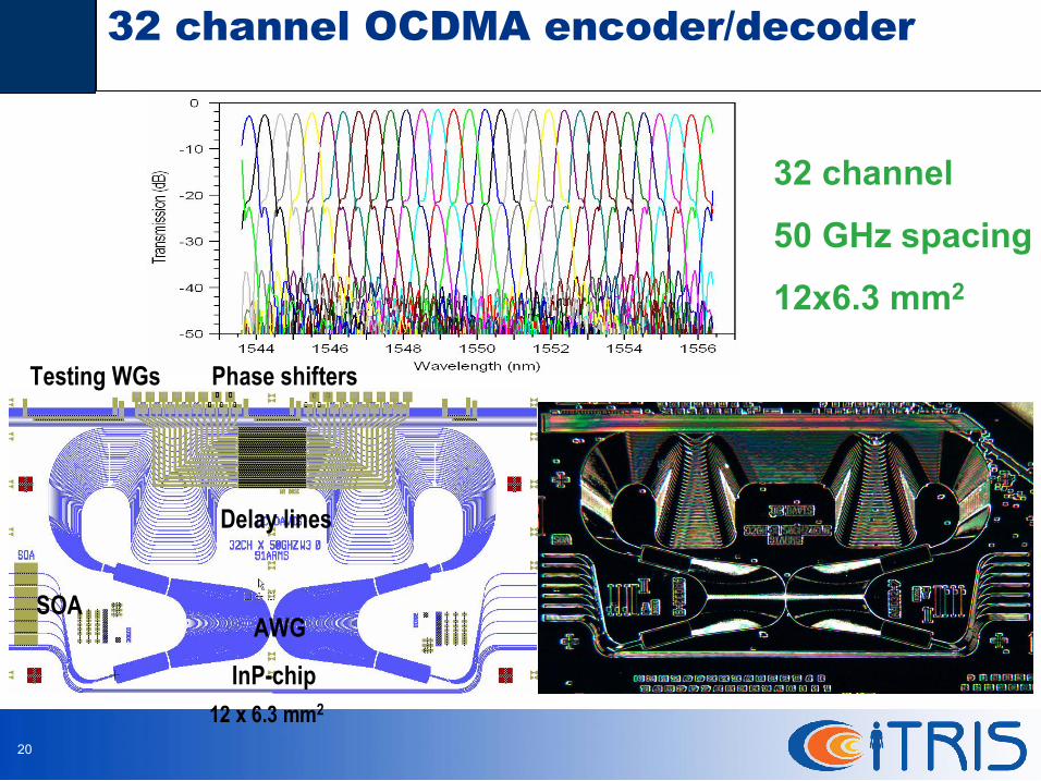
32 channel OCDMA encoder/decoder
12 x 6.3 mm 2
Phase shifters
AWG
Delay lines
InPchip
Testing WGs
SOA
32 channel
50 GHz spacing
12x6.3 mm 2

21
64 channel OCDMA encoder/decoder
16.8 x 11.4 mm 2
Phase shifters
AWG
Delay lines
InPchip
Bond pads Testing WGs
SOA
64 channel
25 GHz spacing
16.8x11.4 mm 2 Monolithically Fabricated Chip
22
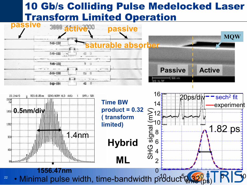
Passive Active
MQW
passive active passive
saturable absorber
1.4nm
1556.47nm
0.5nm/div
0 2 4 6 8 10 12 14 16
10 5 0 5 10 time (ps)
sech 2 fit experiment
SHG signal (mV)
20ps/div
• Minimal pulse width, timebandwidth product 0.32
1.82 ps
Time BW product = 0.32 ( transform limited)
Hybrid
ML
10 Gb/s Colliding Pulse Medelocked Laser Transform Limited Operation

23
0.68 psec CPM laser with Injection Locking & Linear Chirp Correction
5 0 5 0
0.5
1
Time (p.s .)
Field Intensity
Intensity
5 0 5 3
2
1
0
1
2
3
phase (rads)
1545 1550 1555 1560 0
0.5
1
Wavelength (nm)
Spec trum
Intensity
1545 1550 1555 1560
3
2
1
0
1
2
3
phase (rads)
0.6 ps FWHM attainable
0
1
2
3
4
5
10 5 0 5 10 Time (ps)
y = m4+m2*3/(sinh(1.7627/m1*... Error Value
0.003059 0.68336 m1 0.017192 4.7122 m2
0.0018977 0.022452 m3 0.0029284 0.093381 m4
NA 2.6496 Chisq NA 0.99728 R
Dash line: experimental Solid: sech 2 fit with 0.68 ps FWHM
SIMULA
TION
EXPE
RIMEN
T
24
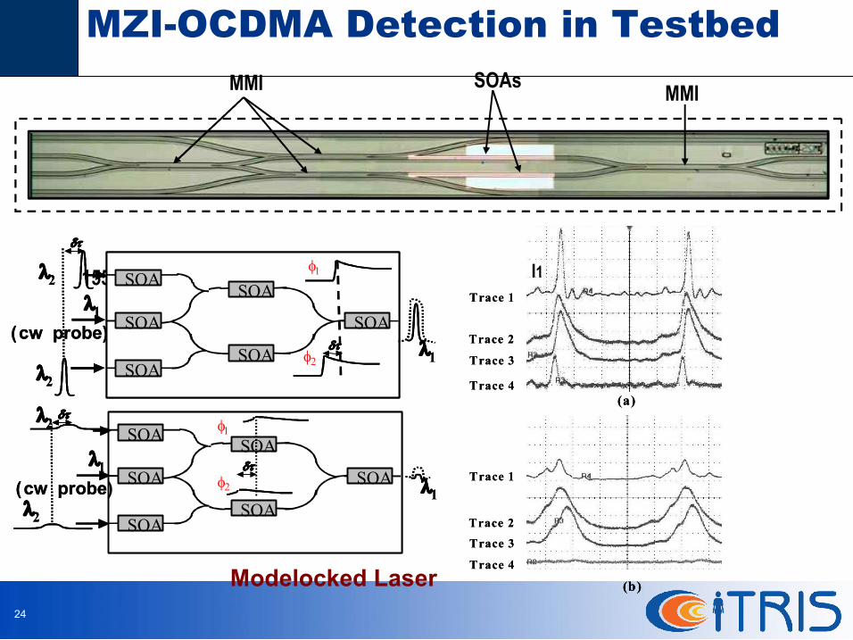
MZIOCDMA Detection in Testbed
Modelocked Laser
(a)
(b)
Trace 1
Trace 2
Trace 3
Trace 4
Trace 1
Trace 2
Trace 3
Trace 4
(a)
(b)
Trace 1
Trace 2
Trace 3
Trace 4
Trace 1
Trace 2
Trace 3
Trace 4
SOAs MMI MMI
I1 1550nm
SOA
SOA
SOA
SOA
SOA
SOA
φ 1
φ 2
δτ
δτ λ 1
λ 2
λ 2 (cw probe) λ 1
SOA
SOA
SOA
SOA
SOA
SOA
φ 1
φ 2
δτ δτ δτ
δτ δτ δτ λ 1
λ 2
λ 2 (cw probe) λ 1
(cw probe)
SOA
SOA
SOA
SOA
SOA
SOA
φ 1
φ 2
δτ
δτ
λ 1
λ 2
λ 2 λ 1
(cw probe)
SOA
SOA
SOA
SOA
SOA
SOA
φ 1
φ 2
δτ δτ δτ
δτ δτ δτ
λ 1
λ 2
λ 2 λ 1

25
14mm
13.5mm
Integrated OCDMA Transceiver
Mask Layout Fabricated Chip
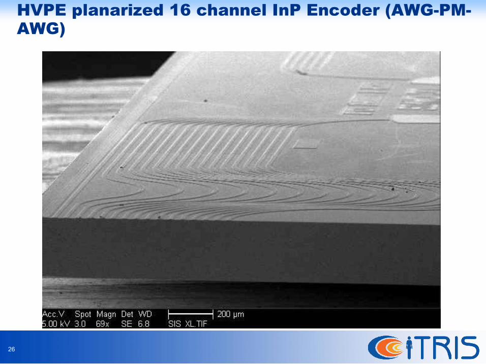
26
HVPE planarized 16 channel InP Encoder (AWGPM AWG)
27
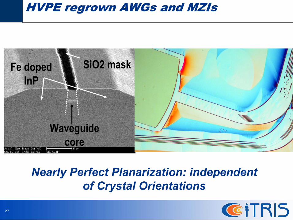
Waveguide core
Fe doped InP
SiO2 mask
HVPE regrown AWGs and MZIs
Nearly Perfect Planarization: independent of Crystal Orientations

28
DEMUX
Substrate
Modelocked Laser
TE Cooler
Silicon Microbench
Output Fiber
Input Fiber
Electrical Contacts
Modelocked Laser
Differential MZI
Photo Diode
OCDMA TRANSMITTER
OCDMA RECEIVER
Data Modulator
Encoder
MUX DEMUX
MUX
Phase Shifter
Decoder
4 cm
1 cm
PXtal Reflectors
OCDMA System on a Chip
29
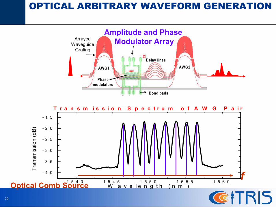
OPTICAL ARBITRARY WAVEFORM GENERATION
AWG1 AWG2
Phase modulators
Bond pads
Delay lines
AWG1 AWG2
Phase modulators
Bond pads
Delay lines
Amplitude and Phase Modulator Array Arrayed
Waveguide Grating
1 5 4 0 1 5 4 5 1 5 5 0 1 5 5 5 1 5 6 0
4 0
3 5
3 0
2 5
2 0
1 5
Transm
ission (d
B)
W a v e l e n g t h ( n m )
T r a n s m i s s i o n S p e c t r u m o f A W G P a i r
f Optical Comb Source

30
Highly Scalable OAWG Encoder/Decoder 320 chx40GHz
9.5mm x 17mm R=100um
Amplitude
Modulator Phase
Modulator
30.00
20.00
10.00
0.00
1.5 1.525 1.55 1.575 1.6
Wavelength [um]
Loss [d
B]
32ch x 400GHz

31
Nano Photonic Interconnect
Ref. IBM
Photo from: J. D. Joannopoulos, P. R. Villeneuve, and S. Fan, Nature, vol. 386, pp. 143 (1997)

32
“Client”
“Server”
Collaborative Applications on CITRISnet
CITRIS net Nodes
PoP node
DARK Fiber
Circuit Connection OC48 or lower
In the Future CITRISNet, perhaps Optical Routers
Optical Access Nodes Photonic Interconnected Nano Processors with Integrated Micro/Nano Photonics Inside

33
saturable absorber
passive active passive
nInP
1.15Q WG MQW
Passive Active pInP
500nm
MQW
Pmetal
1.15Q wave guiding core
Regrown Fe doped InP
10 Gb/s Colliding Pulse Medelocked Lasers with Active/Passive Integration