systems design & programming memory cmpe 310squire/memory2.pdf · systems design &...
TRANSCRIPT

1
Systems Design & Programming CMPE 310Memory
Memory Address Decoding
The processor can usually address a memory space that is much larger than the memory space covered by an individual memory chip.
In order to splice a memory device into the address space of the processor, decoding is nec-essary.
For example, the 8088 issues 20-bit addresses for a total of 1MB of memory address space.
However, the BIOS on a 2716 EPROM has only 2KB of memory and 11 address pins.
A decoder can be used to decode the additional 9 address pins and allow the EPROM to be placed in any 2KB section of the 1MB address space.

2
Systems Design & Programming CMPE 310Memory
Memory Address Decoding
A0A1
A10
O0O1
O7
... ...
CS
RD of 8088/86 Or MRDC bus signal.
2716
IO/M
A19
A18
A17
A16
A15
A14
A13
A12
A11
Address Bus Data Bus
Logic 0 when A11 through A19 are all 1.
(2K X 8)
(Book shows OE connection for RD but chip definition does NOT have this pin)
EPROM

3
Systems Design & Programming CMPE 310Memory
Memory Address Decoding
To determine the address range that a device is mapped into:
This 2KB memory segment maps into the reset location of the 8086/8088 (FFFF0H).
NAND gate decoders are not often usedLarge fan-in NAND gates are not efficientMultiple NAND gate IC's might be required to perform such decodingRather the 3-to-8 Line Decoder (74LS138) is more common.
1111 1111 1XXX XXXX XXXX
A19 - A11 A10 - A0
1111 1111 1000 0000 0000 (FF800H)
To
1111 1111 1111 1111 1111 (FFFFFH)
4
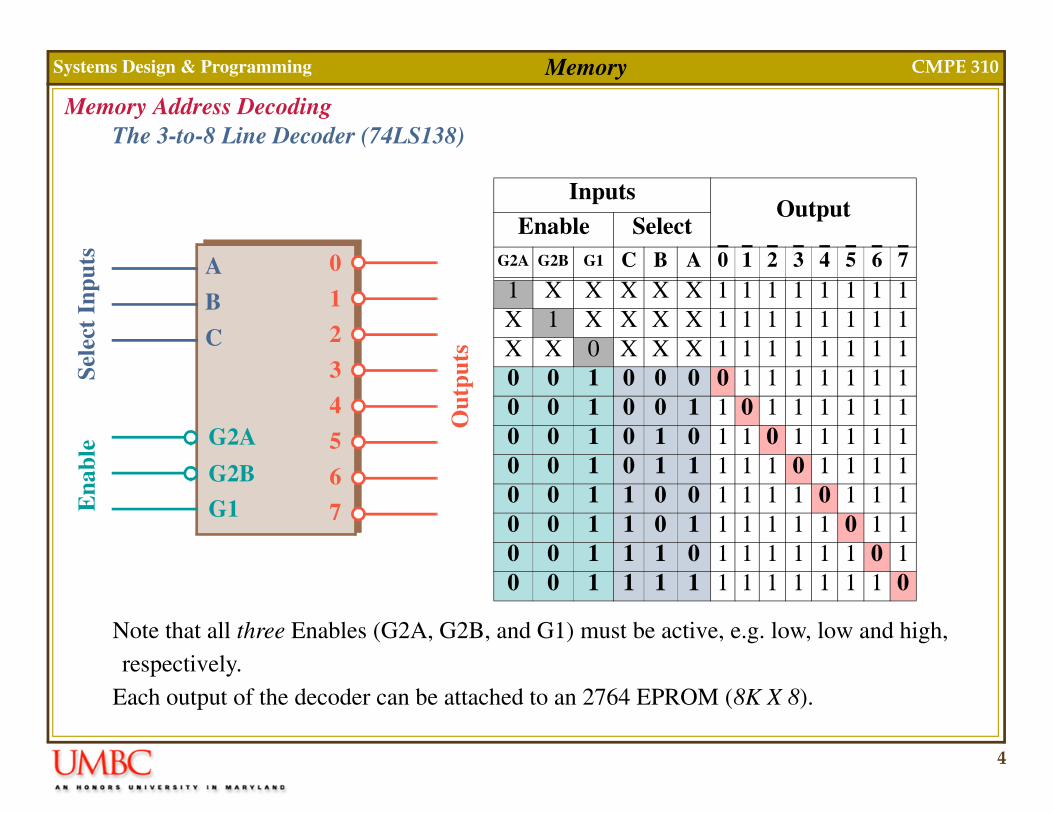
Systems Design & Programming CMPE 310Memory
Memory Address DecodingThe 3-to-8 Line Decoder (74LS138)
Note that all three Enables (G2A, G2B, and G1) must be active, e.g. low, low and high, respectively.
Each output of the decoder can be attached to an 2764 EPROM (8K X 8).
G2A
G2B
G1
A
B
C
0
1
2
3
4
5
6
7Ena
ble
Sele
ct I
nput
s
Out
puts
InputsOutput
Enable SelectG2A G2B G1 C B A 0 1 2 3 4 5 6 7
1 X X X X X 1 1 1 1 1 1 1 1X 1 X X X X 1 1 1 1 1 1 1 1X X 0 X X X 1 1 1 1 1 1 1 10 0 1 0 0 0 0 1 1 1 1 1 1 10 0 1 0 0 1 1 0 1 1 1 1 1 10 0 1 0 1 0 1 1 0 1 1 1 1 10 0 1 0 1 1 1 1 1 0 1 1 1 10 0 1 1 0 0 1 1 1 1 0 1 1 10 0 1 1 0 1 1 1 1 1 1 0 1 10 0 1 1 1 0 1 1 1 1 1 1 0 10 0 1 1 1 1 1 1 1 1 1 1 1 0
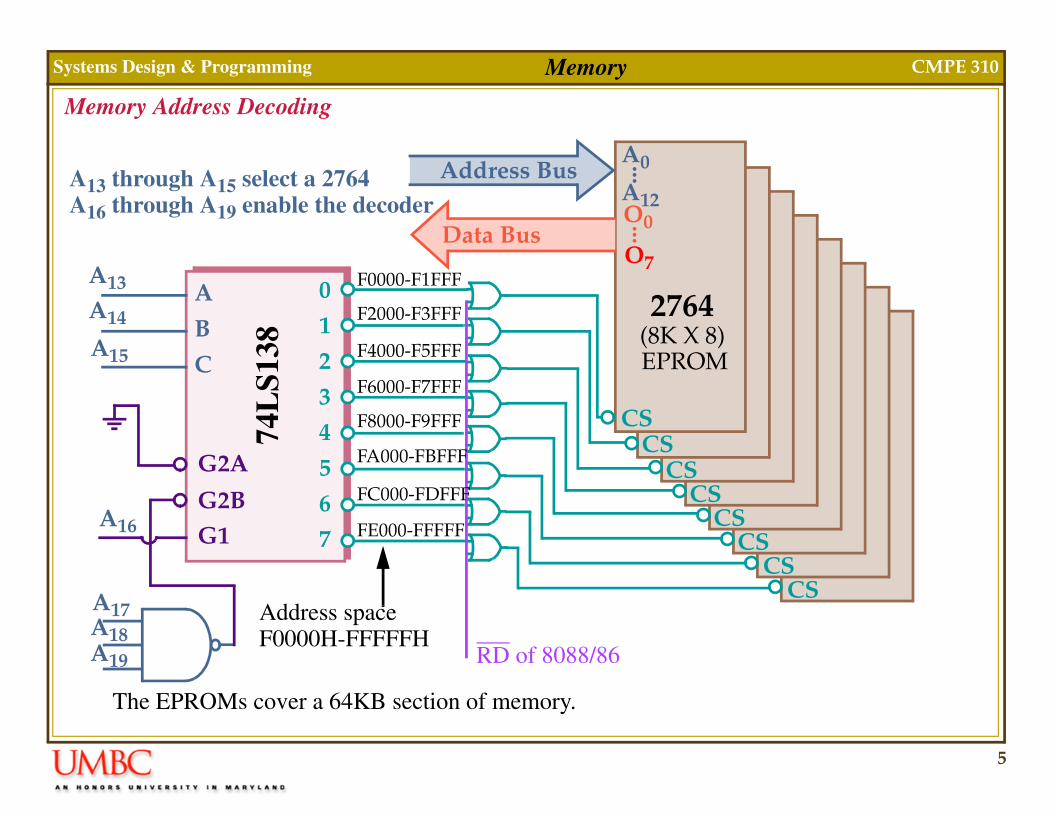
5
Systems Design & Programming CMPE 310Memory
Memory Address Decoding
The EPROMs cover a 64KB section of memory.
G2A
G2BG1
A
B
C
01234567
A0
A12O0
O7
......
CS
2764
A16
A17A18A19
A13
A14
A15
CSCS
CSCS
CSCS
CS
RD of 8088/86
Data Bus
Address Bus
F2000-F3FFF
F0000-F1FFF
F4000-F5FFF
F6000-F7FFF
F8000-F9FFF
FA000-FBFFF
FC000-FDFFF
FE000-FFFFF
Address spaceF0000H-FFFFFH
A13 through A15 select a 2764 A16 through A19 enable the decoder
(8K X 8)
74L
S138 EPROM
6
Systems Design & Programming CMPE 310Memory
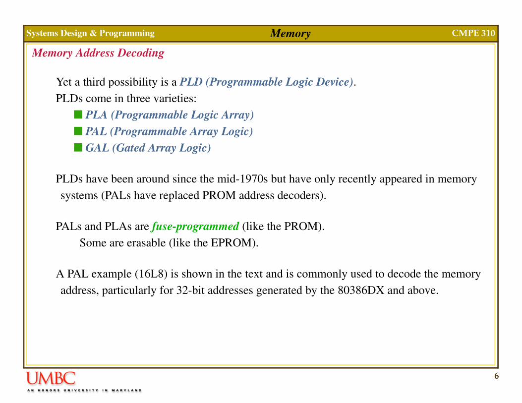
Memory Address Decoding
Yet a third possibility is a PLD (Programmable Logic Device).PLDs come in three varieties:
PLA (Programmable Logic Array) PAL (Programmable Array Logic) GAL (Gated Array Logic)
PLDs have been around since the mid-1970s but have only recently appeared in memory systems (PALs have replaced PROM address decoders).
PALs and PLAs are fuse-programmed (like the PROM).Some are erasable (like the EPROM).
A PAL example (16L8) is shown in the text and is commonly used to decode the memory address, particularly for 32-bit addresses generated by the 80386DX and above.
7
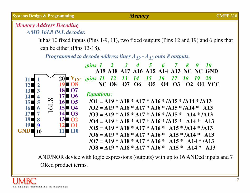
Systems Design & Programming CMPE 310Memory
Memory Address DecodingAMD 16L8 PAL decoder.
It has 10 fixed inputs (Pins 1-9, 11), two fixed outputs (Pins 12 and 19) and 6 pins that can be either (Pins 13-18).
AND/NOR device with logic expressions (outputs) with up to 16 ANDed inputs and 7 ORed product terms.
O3
1234567
15
11
2019
16
16L
8 1718
I4I5I6I7
VCC
I3I2
O6
O8I1
O4O5
O7
98
10121314
I8I9
GND
O2O1I10
;pins 1 2 3 4 5 6 7 8 9 10A19 A18 A17 A16 A15 A14 A13 NC NC GND
;pins 11 12 13 14 15 16 17 18 19 20NC O8 O7 O6 O5 O4 O3 O2 O1 VCC
Equations:/O1 = A19 * A18 * A17 * A16 * /A15 * /A14 * /A13/O2 = A19 * A18 * A17 * A16 * /A15 * /A14 * A13/O3 = A19 * A18 * A17 * A16 * /A15 * A14 * /A13/O4 = A19 * A18 * A17 * A16 * /A15 * A14 * A13/O5 = A19 * A18 * A17 * A16 * A15 * /A14 * /A13/O6 = A19 * A18 * A17 * A16 * A15 * /A14 * A13/O7 = A19 * A18 * A17 * A16 * A15 * A14 * /A13/O8 = A19 * A18 * A17 * A16 * A15 * A14 * A13
Programmed to decode address lines A19 - A13 onto 8 outputs.

8
Systems Design & Programming CMPE 310Memory
8088 and 80188 (8-bit) Memory Interface
The memory systems sees the 8088 as a device with: 20 address connections (A19 to A0). 8 data bus connections (AD7 to AD0). 3 control signals, IO/M, RD, and WR.
We'll look at interfacing the 8088 with: 32K of EPROM (at addresses F8000H through FFFFFH). 512K of SRAM (at addresses 00000H through 7FFFFH).
The EPROM interface uses a 74LS138 (3-to-8 line decoder) plus 8 2732 (4K X 8) EPROMs.
The EPROM will also require the generation of a wait state.The EPROM has an access time of 450ns.The 74LS138 requires 12ns to decode.The 8088 runs at 5MHz and only allows 460ns for memory to access data.A wait state adds 200ns of additional time.

9
Systems Design & Programming CMPE 310Memory
8088 and 80188 (8-bit) EPROM Memory Interface
The 8088 cold starts execution at FFFF0H. JMP to F8000H occurs here.
G2A
G2BG1
A
B
C
01234567
A0
A11O0
O7
......
CS
2732
A15
A17A18
A19
A12
A13
A14
CSCS
CSCS
CSCS
CS
RD
Data Bus
Address Bus
Address space
F8000H-FFFFFH
(4K X 8)
74LS138
OE
A16
WAIT
IO/M
5V
1K
To wait state generator

10
Systems Design & Programming CMPE 310Memory
8088 and 80188 (8-bit) RAM Memory Interface
A0
A14
O0
O7
... ...
CS
A18
A19
CSCSCSCS
CSCSCS
OE
IO/M
WE
CSCSCSCS
CSCSCS
A0
A14
O0
O7
... ...
CSOEWE
Data Bus
(32K
X 8
)
WR
A15A16A17
1G 2G
74L
S244
Buf
fer
RD
G
Dir
74L
S245
BD
Buf
fer
G2AG2B
G1
ABC
01234567
G2AG2B
G1
ABC
01234567
Address Bus
74L
S138
A14
A9A10A11A12A13
1G 2G74
LS2
44B
uffe
r
A8
G2AG2B
G1
ABC
01234567
A6A7
A0A1A2A3A4A5
1G 2G
74L
S244
Buf
fer
6225
6
(32K
X 8
)62
256
3
2
74L
S138
74L
S138
4

11
Systems Design & Programming CMPE 310Memory
8088 and 80188 (8-bit) RAM Memory Interface
The 16 62256s on the previous slide are actually SRAMs.Access times are on order of 10ns.
Flash memory can also be interfaced to the 8088 (see text).However, the write time (400ms!) is too slow to be used as RAM (as shown in the text).
Parity CheckingParity checking is used to detect single bit errors in the memory.
The current trend is away from parity checking.
Parity checking adds 1 bit for every 8 data bits. For EVEN parity, the 9th bit is set to yield an even number of 1's in all 9 bits. For ODD parity, the 9th bit is set to make this number odd.
For 72-pin SIMMs, the number of data bits is 32 + 4 = 36 (4 parity bits).
12
Systems Design & Programming CMPE 310Memory
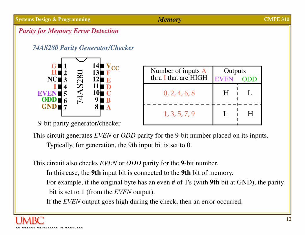
Parity for Memory Error Detection
74AS280 Parity Generator/Checker
This circuit generates EVEN or ODD parity for the 9-bit number placed on its inputs.Typically, for generation, the 9th input bit is set to 0.
This circuit also checks EVEN or ODD parity for the 9-bit number.In this case, the 9th input bit is connected to the 9th bit of memory.For example, if the original byte has an even # of 1's (with 9th bit at GND), the parity bit is set to 1 (from the EVEN output).
If the EVEN output goes high during the check, then an error occurred.
A
1234567
98
1413
10
74A
S280
1112
IEVEN
ODDGND
VCC
NCH
D
FG
BC
E
9-bit parity generator/checker
Number of inputs Athru I that are HIGH
OutputsEVEN ODD
0, 2, 4, 6, 8
1, 3, 5, 7, 9
H L
L H

13
Systems Design & Programming CMPE 310Memory
Parity for Memory Error Detection
A0
A14
O0
O7
... ...
CS
A18
OE
RESET
WEWR
A15A16A17
RD
G2AG2B
G1
ABC
01234567
74L
S138
(32K
X 8
)62
256
A0
A14
O0
O7
... ...
CSOEWE
(32K
X 8
)62
256
6287
(64K
X 1
)
A0
A15
...
CEWE
ABCDEFGHI
ABCDEFGHI
74L
S280
74L
S280
EVENODD
EVENODD
74L
S74Q
Q
D
CLK
DODI
Generator
Checker
IO/M
A19
Dat
a B
usClear
NMI
Address Bus
14
Systems Design & Programming CMPE 310Memory
Error Detection
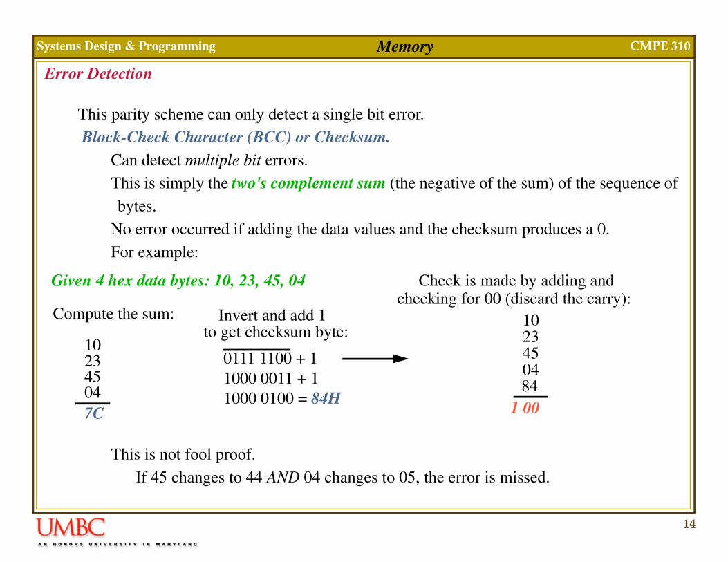
This parity scheme can only detect a single bit error. Block-Check Character (BCC) or Checksum.
Can detect multiple bit errors.This is simply the two's complement sum (the negative of the sum) of the sequence of bytes.
No error occurred if adding the data values and the checksum produces a 0.For example:
This is not fool proof. If 45 changes to 44 AND 04 changes to 05, the error is missed.
Compute the sum:
Given 4 hex data bytes: 10, 23, 45, 04
102345047C
Invert and add 1
0111 1100 + 11000 0011 + 11000 0100 = 84H
to get checksum byte: 10234504
1 00
Check is made by adding and
84
checking for 00 (discard the carry):
15
Systems Design & Programming CMPE 310Memory
Error Detection
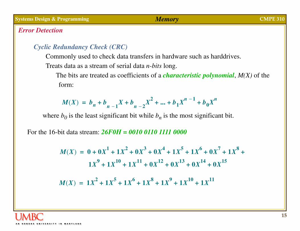
Cyclic Redundancy Check (CRC)Commonly used to check data transfers in hardware such as harddrives.Treats data as a stream of serial data n-bits long.
The bits are treated as coefficients of a characteristic polynomial, M(X) of the form:
M X( ) bn bn 1− X b
n 2− X2 ... b1X
n 1−b0X
n+ + + + +=
M X( ) 0 0X1 1X2 0X3 0X4 1X5 1X6 0X7 1X8+ + + + + + + + +=
where b0 is the least significant bit while bn is the most significant bit.
For the 16-bit data stream: 26F0H = 0010 0110 1111 0000
1X9 1X10 1X11 0X12 0X13 0X14 0X15+ + + + + +
M X( ) 1X2 1X5 1X6 1X8 1X9 1X10 1X11+ + + + + +=
16
Systems Design & Programming CMPE 310Memory
Error Detection
Cyclic Redundancy Check (CRC) (cont.)
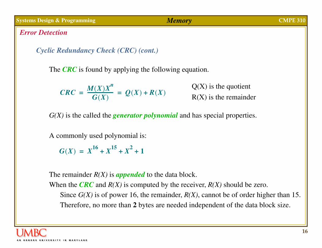
The CRC is found by applying the following equation.
G(X) is the called the generator polynomial and has special properties.
A commonly used polynomial is:
The remainder R(X) is appended to the data block.When the CRC and R(X) is computed by the receiver, R(X) should be zero.
Since G(X) is of power 16, the remainder, R(X), cannot be of order higher than 15.Therefore, no more than 2 bytes are needed independent of the data block size.
CRC M X( )Xn
G X( )--------------------- Q X( ) R X( )+= =
Q(X) is the quotient
R(X) is the remainder
G X( ) X16
X15
X2 1+ + +=

17
Systems Design & Programming CMPE 310Memory
Error Detection Cyclic Redundancy Check (CRC) (cont.)
M X( )X16
G X( )------------------------- X
27X
26X
25X
24X
22X
21X
18+ + + + + +
X16
X15
X2
1+ + +--------------------------------------------------------------------------------------------------------------=
X16
X15
X2
1+ + + X27
X26
X25
X24
X22
X21
X18
+ + + + + +
X27
X26
+ X13
X11
++
X25
X24
X22
X21
X18
+ + + +
X25
X24
+ X11
X9
+
X22
X21
X18
+ + X9
+
+
X22
X21
+ X8
X6
++
X18 X
9X
8X
6+ ++
X13+
+ X13
X18
X17
+ X4
X2
+
X17
X13
+
+
X17
X16
+ X3
X+...
X11
X9
X6
X2
X 1+ + + + +
X13
X11
++
X9
X8
X6
X4
X2
+ + + ++
R X( ) X15 X13 X9 X8 X6 X4 X3 X 1+ + + + + + + +=
Final Solution is:
Value appended is the reverse coefficient value 1101 1010 1100 0101 = DAC5H
18
Systems Design & Programming CMPE 310Memory
Error Correction
Parity, BCC and CRC are only mechanisms for error detection.The system is halted if an error is found in memory.
Error correction is starting to show up in new systems.SDRAM has ECC (Error Correction Code).
Correction will allow the system can continue operating.If two errors occur, they can be detected but not corrected.Error correction will of course cost more in terms of extra bits.
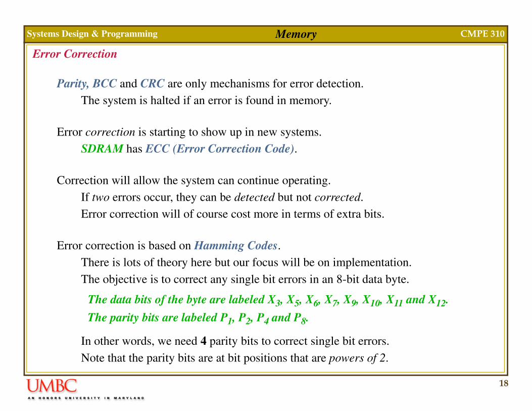
Error correction is based on Hamming Codes.There is lots of theory here but our focus will be on implementation.The objective is to correct any single bit errors in an 8-bit data byte.
In other words, we need 4 parity bits to correct single bit errors.Note that the parity bits are at bit positions that are powers of 2.
The data bits of the byte are labeled X3, X5, X6, X7, X9, X10, X11 and X12.
The parity bits are labeled P1, P2, P4 and P8.

19
Systems Design & Programming CMPE 310Memory
Error CorrectionHamming Codes (cont).
P1 is generated by computing the parity of X3, X5, X7, X9, X11, X13, X15.
These numbers have a 1 in bit position 1 of the subscript in binary.
0 0 0 00 0 0 10 0 1 00 0 1 10 1 0 00 1 0 10 1 1 00 1 1 11 0 0 01 0 0 11 0 1 01 0 1 11 1 0 01 1 0 11 1 1 01 1 1 1
P1P2
P3
P4
34
210
56789101112131415
1234
P1 is assigned even parity using X3, X5, X7, X9, X11, X13, X15
P2 is assigned even parity using X3, X6, X7, X10, X11, X14, X15
P3 is assigned even parity using X5, X6, X7, X12, X13, X14, X15
P4 is assigned even parity using X9, X10, X11, X12, X13, X14, X15
Note that each data bit is used in the parity computation of at least 2 P bits.
Given data byte: 11010010
P1 uses blue bits:
Not used since we are correcting byte data.
1 1 0 1 0 0 1 035679101112
P1 even parity is 1.
P2 uses brown bits:
1 1 0 1 0 0 1 035679101112
P2 even parity is 1.
1 1 0 1 0 0 1 0
1 1 0 1 0 0 1 0
P3 uses cyan bits:
P3 even parity is 0.
P4 uses purple bits:
P4 even parity is 1.
35679101112
35679101112
20
Systems Design & Programming CMPE 310Memory
Error Correction
Hamming Codes (cont).
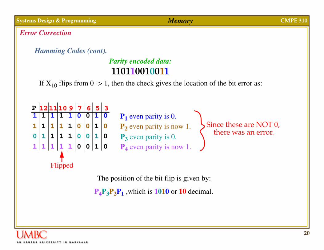
110110010011Parity encoded data:
If X10 flips from 0 -> 1, then the check gives the location of the bit error as:
1 1 1 1 1 0 0 1 035679101112
P1 even parity is 0. 1 1 1 1 1 0 0 1 0 P2 even parity is now 1. 0 1 1 1 1 0 0 1 0
1 1 1 1 1 0 0 1 0P3 even parity is 0. P4 even parity is now 1.
Flipped
P
The position of the bit flip is given by:
Since these are NOT 0,there was an error.
P4P3P2P1 ,which is 1010 or 10 decimal.

21
Systems Design & Programming CMPE 310Memory
Parity for Memory Error Correction
The 74LS636 corrects errors by storing 5 parity bits with each byte of data.The pinout consists of: 8 data I/O pins 5 check bit I/O pins 2 control pins 2 error outputs
Single error flag (SEF)Double error flag (DEF).
CB2
1234567
15
11
2019
16
74L
S636 17
18DB2DB3DB4DB5
VCC
DB1DB0
S0
SEFDEF
CB1CB0
S1
98
10121314
DB6DB7
GND
CB3NCCB4
See the text for an example of its use in a circuit.