systemization of rfid tag antenna design based on … · 2017-01-31 · designs to compliment...
TRANSCRIPT

i
Systemization of RFID Tag Antenna Design Based on
Optimization Techniques and Impedance Matching
Charts
By
Munam Butt
Thesis presented to the
Faculty of Graduate and Postdoctoral Studies
In partial fulfillment of the requirements for the degree of
Master of Applied Science
in
Electrical and Computer Engineering
Ottawa-Carleton Institute for Electrical and Computer Engineering
Department of Electrical Engineering and Computer Science
Faculty of Engineering
University of Ottawa
Ottawa, Ontario, Canada, April, 2012
Copyright ©
Munam Butt, Ottawa, Canada, 2012

ii
ABSTRACT
The performance of commercial Radio Frequency Identification (RFID) tags is primarily
limited by present techniques used for tag antenna design. Currently, industry techniques
rely on identifying the RFID tag application (books, clothing, etc.) and then building antenna
prototypes of different configurations in order to satisfy minimum read range requirements.
However, these techniques inherently lack an electromagnetic basis and are unable to
provide a low cost solution to the tag antenna design process. RFID tag performance
characteristics (read-range, chip-antenna impedance matching, surrounding environment)
can be very complex, and a thorough understanding of the RFID tag antenna design may be
gained through an electromagnetic approach in order to reduce the tag antenna size and the
overall cost of the RFID system.
The research presented in this thesis addresses RFID tag antenna design process for
passive RFID tags. With the growing number of applications (inventory, supply-chain,
pharmaceuticals, etc), the proposed RFID antenna design process demonstrates procedures
to design tag antennas for such applications. Electrical/geometrical properties of the antennas
designed were investigated with the help of computer electromagnetic simulations in order
to achieve optimal tag performance criteria such as read range, chip-impedance matching,
antenna efficiency, etc. Experimental results were performed on the proposed antenna
designs to compliment computer simulations and analytical modelling.

iii
ACKNOWLEDGEMENTS
I would have never been able to finish my thesis without the support and guidance from
everyone who helped me every step of the way. I am grateful for the opportunity to complete this
thesis and would like to acknowledge a few individuals who deserve my heartfelt thanks.
I offer my sincerest gratitude to my supervisor at the School of Electrical Engineering and
Computer Science at the University of Ottawa, Dr. Mustapha C.E. Yagoub. I am grateful for
all his guidance, support, motivation and patience throughout the process of my research
work.
I would also like to express my gratitude to my colleagues Rijwal C.R., Alexi Borisenko, as
well as the Lab Coordinator Mr. Alain Le Hénaff for analyzing my work critically and providing
me with suggestions.
Finally, I would like to thank my parents, my brothers, my sister, my brother-in-law, and my
nephews, for their support and encouragement throughout my graduate studies at the University
of Ottawa.

iv
TABLE OF CONTENTS
ABSTRACT ............................................................................................................................. ii
ACKNOWLEDGEMENTS .................................................................................................... iii
LIST OF FIGURES ................................................................................................................ vii
LIST OF TABLES ................................................................................................................... x
CHAPTER 1 INTRODUCTION ............................................................................................. 1
1.1 Motivation ...................................................................................................................... 1
1.2 Thesis Scope and Outline ............................................................................................... 2
1.3 Contributions .................................................................................................................. 3
CHAPTER 2 – Background to RFID and Antenna Theory fundamentals .............................. 4
2.1 Introduction to RFID technology ................................................................................... 4
2.1.1 History of RFID ...................................................................................................... 6
2.1.2 Overview of RFID Technology .............................................................................. 7
2.1.3 RFID Technology Applications .............................................................................. 9
2.1.4 Benefits of RFID ..................................................................................................... 9
2.1.5 RFID Antenna Characteristics .............................................................................. 10
2.1.6 RFID Tags ............................................................................................................. 13
2.2 RF in RFID ................................................................................................................... 18
2.2.1 Antenna fundamentals ........................................................................................... 19
2.2.2 Coupling Mechanisms ........................................................................................... 23
2.3 Chapter Summary ......................................................................................................... 24
CHAPTER 3 – RFID tag antenna design requirements and testing procedures .................... 26
3.1 Tag Performance Criteria ............................................................................................. 26
3.2 Tag Design Process ...................................................................................................... 29
3.3 Tag Testing Procedures ................................................................................................ 31
3.4 Chapter Summary ......................................................................................................... 33
Chapter 4 - Conjugate Impedance Matching Techniques ...................................................... 35
4.1 T-Match ........................................................................................................................ 35

v
4.2 Inductively Coupled Loop ............................................................................................ 37
4.3 Nested Slot .................................................................................................................... 39
4.4 HFSS Modified T-Match Simulation ........................................................................... 41
4.4.1 T-Match Antenna Design ...................................................................................... 41
4.4.2 T-Match Simulation Results ................................................................................. 42
4.5 HFSS Inductively Coupled Loop Simulation ............................................................... 46
4.5.1 Inductively Coupled Loop Antenna Design .......................................................... 46
4.5.2 Inductively Coupled Loop Simulation Results ..................................................... 47
4.6 HFSS Nested Slot Simulation ...................................................................................... 49
4.6.1 Nested Slot Antenna Design ................................................................................. 49
4.6.2 Nested Slot Simulation Results ............................................................................. 50
4.7 Summary ....................................................................................................................... 53
CHAPTER 5 – Classification of commercially available RFID tags .................................... 54
5.1 Dipoles .......................................................................................................................... 54
5.1.1 Printed Dipoles ...................................................................................................... 56
5.1.2 Radiating Resistance ............................................................................................. 56
5.2 Size Reduction Techniques .......................................................................................... 58
5.2.1 Meandering Diploes .............................................................................................. 58
5.2.2 Inverted-F Configurations ..................................................................................... 61
5.3 Classification of RFID Tags based on application. ...................................................... 62
5.4 Chapter Summary ......................................................................................................... 67
CHAPTER 6 – Simulation of antennas design using HFSS .................................................. 68
6.1 Proposed Antenna Designs ........................................................................................... 68
6.2 Optimization of antenna design using HFSS simulations ............................................ 74
6.2.1 Simulation results without optimization ............................................................... 74
6.2.2 Simulation results with optimization .................................................................... 82
6.3 Discussion of Simulation Results ............................................................................... 102
6.4 Chapter Summary ....................................................................................................... 104
CHAPTER 7 – Experimental Measurements and Results ................................................... 106
7.1 Read Range ................................................................................................................. 107
7.2 Impedance Measurement ............................................................................................ 109

vi
7.3 Comparison of simulated and measured results ......................................................... 112
7.4 Chapter Summary ....................................................................................................... 117
Chapter 8 – Conclusion ........................................................................................................ 118
8.1 Contribution ................................................................................................................ 118
8.2 Future work ................................................................................................................ 119
REFERENCES ..................................................................................................................... 120

vii
LIST OF FIGURES
Figure 2.1 Overview of Auto-ID technologies [11] ...................................................................5
Figure 2.2 Main Components of an RFID system [13] ..............................................................5
Figure 2.3 RFID Sytem divided into layers [11] ........................................................................7
Figure 2.4 RFID Sytem related to EM terminology [11] .........................................................11
Figure 2.5 RFID tag classification [11] ...................................................................................14
Figure 2.6 Field Regions [19] ..................................................................................................19
Figure 2.7 Far field approximation of R for a finite length dipole [19] ...................................21
Figure 2.8 Radiation pattern of dipoles of various lengths [18] ..............................................22
Figure 2.9 Power supply to an inductively coupled tag from magnetic [11] ..........................24
Figure 2.10 Modulated backscatter by modulation of the transponder impedance [19] ..........25
Figure 3.1 Antenna impedance, chip impedance and read range [5] .......................................27
Figure 3.2 Tag performance chart: contours of the constant normalized range [5] .................28
Figure 3.3 RFID tag antenna design process [5] .....................................................................30
Figure 3.4 RFID tag range measurement using anacheoic chamber [5] ..................................32
Figure 3.5 Measurement setup [23] .........................................................................................33
Figure 3.6 Half-antenna mounted on the plate [23] .................................................................33
Figure 3.7 Tag operating above a ground plane [10] ...............................................................33
Figure 4.1 T-match of the planar dipole with its equivalent circuit [7] ...................................36
Figure 4.2 Matching chart for the T-match layout [7] .............................................................37
Figure 4.3 Example of an embedded T-match feed [7] ...........................................................37
Figure 4.4 Inductively coupled feed with its equivalent circuit [32] ......................................38
Figure 4.5 Matching chart for the loop-fed dipole [7] .............................................................39
Figure 4.6 Geometry of a nested-slot suspended patch [31],[22] ............................................40
Figure 4.7 A tag antenna attached to the human body [31] .....................................................40
Figure 4.8 Matching chart for the nested slot layout [7] .........................................................41
Figure 4.9 T-Match RFID antenna design layout ....................................................................42
Figure 4.10 T-Match configuration for planar dipoles [7] .......................................................42
Figure 4.11 Simulation results showing the return loss of the antenna ...................................43
Figure 4.12 Simulation antenna input impedance with respect to frequency ..........................43
Figure 4.13 Simulated antenna 3-D antenna gain pattern for T-Match ...................................44
Figure 4.14 Inductively couple loop RFID antenna design layout ..........................................46
Figure 4.15 Inductively couple loop configuration for planar dipole [7] ................................46
Figure 4.16 Simulation results showing the return loss of the antenna ...................................44
Figure 4.17 Simulated antenna input impedance with respect to frequency ............................48
Figure 4.18 Simulated antenna 3-D gain pattern ane radiation pattern ....................................48
viii
Figure 4.19 The nested-slot RFID antenna design layout ........................................................50
Figure 4.20 The geometry of the nested-slot suspended patch [7] ..........................................50
Figure 4.21 Simulation results showing the return loss of the antenna ...................................51
Figure 4.22 Simulation antenna input impedance with respect to frequency .........................51
Figure 4.23 Simulated antenna 3-D gain pattern and antenna radiation pattern ......................52
Figure 5.1 Variety of commercially avaialable tags [10] ........................................................54
Figure 5.2 Dipole antenna [33] ................................................................................................55
Figure 5.3 Simple circuit model of dipole antenna near reonance [10] ...................................55
Figure 5.4 Relationship between cylindrical and ribbon dipoles [10] .....................................56
Figure 5.5 A meander-line antenna (f=915 MHz) with an indctively coupled loop feed ........57
Figure 5.6 Examples of capacitive tip-loaded tags [10] ...........................................................57
Figure 5.7 Example of spiral-loaded tag [10] ..........................................................................58
Figure 5.8 The geometry of the meander line antenna with multiple unequal turns [7] ..........59
Figure 5.9 An equi-spaced meander line antenna (f=953 MHz) with T-match feed [36] ........59
Figure 5.10 A meander-line antenna (f=915 MHz) with an inductively coupled loop [37] ....59
Figure 5.11 A meander-line antenna (f=920 MHz) with a loading bar [37] ............................60
Figure 5.12 A multi-conductor antenna (f=915 MHz) with double T-match scheme [38] ......60
Figure 5.13 A text shaped meander-line antenna (f=915 MHz) [39] .......................................60
Figure 5.14 A multi-conductor meander-line tag (f=915 MHz) [7] .........................................61
Figure 5.15 Folded antennas [7] ...............................................................................................61
Figure 5.16 The matching chart for the co-planar inverted-F antenna geometry [7] ...............62
Figure 5.17 A conventional two-layer PIFA (f=870 MHz) with square conductor [7] ...........63
Figure 5.18 A two-layer double PIFA tag [7] ..........................................................................63
Figure 5.19 A co-planar IFA (f=870 MHz) [41] ......................................................................63
Figure 6.1 Dimensions of the proposed antenna designs .........................................................72
Figure 6.2 Simulation results showing the return loss of the proposed antennas ....................75
Figure 6.3 Simulation results showing the impedance of the proposed antennas ....................77
Figure 6.4 Simulation results showing the 3-D gain pattern and radiation pattern .................79
Figure 6.5 Optimization of specific antenna parts for improving tag performance .................82
Figure 6.6 Dimensions of the antenna shown to exceed the dimensions of the substrate .......83
Figure 6.7 Dimensions of the antenna are within the dimensions of the substrate ..................83
Figure 6.8 Simulation results of inductive loop optimization of the proposed antennas ........84
Figure 6.9 Simulation results of capacitive tip optimization of the proposed antennas ..........87
Figure 6.10 Simulation results of height optimization of the proposed antennas ...................90
Figure 6.11 Simulation results of width optimization of the proposed antennas ....................94
Figure 6.12 Simulation results of substrate optimization of the proposed antennas ...............98
Figure 6.13 Passive RFID transponder for high frequency (13.56 MHz) application ...........103
Figure 6.14 Inductive coil antenna design for high frequency (13.56 MHz) application .....104
Figure 7.1 Pictures of the fabricated antenna designs ...........................................................106
Figure 7.2a Measurement setup. ............................................................................................108

ix
Figure 7.2b RFID tag place on a foam stand .........................................................................108
Figure 7.3a Half tag placed on plate. .....................................................................................109
Figure 7.3b Half tag mounted on a brass sheet. ....................................................................109
Figure 7.4 RF cable connecting the VNA to the SMA connector .........................................109
Figure 7.5a Impedance of the VNA with a matched 50 Ohm load ........................................110
Figure 7.5b Return loss of the VNA with a matched 50 Ohm load ......................................110
Figure 7.6 Measured impedance and return loss of the proposed antennas ..........................111
Figure 7.7 Measured results versus the simulation results for the proposed antennas. .........114
Figure 7.8a Industry standard HF tag antenna design ............................................................116
Figure 7.8b Fabricated antenna E ...........................................................................................116
Figure 7.9 Mobile application 'tag info' used to read the contactless card ............................116

x
LIST OF TABLES
Table 2.1 RFID Technology compared to traditional barcodes [1] .........................................10
Table 2.2 Effect of polarization mismatch resulting in different values for PLF [19]. ............12
Table 2.3 RFID tag types based on power source ....................................................................15
Table 2.4 RFID classes and their functionality ........................................................................17
Table 4.1 Simulated antenna parameters T-match ...................................................................45
Table 4.2 Simulated antenna parameters Inductive loop .........................................................49
Table 4.3 Simulated antenna parameters Nested Slot .............................................................52
Table 4.4 The simulated return loss and impedance value comparison ...................................52
Table 5.1 Antennas marketed by Avery Dennison ..................................................................64
Table 5.2 Family of RFID tags based on application ...............................................................67
Table 6.1 Family of RFID tags based on proposed antennas ...................................................68
Table 6.2 ASIC chips used for antennas ..................................................................................69
Table 6.3 Proposed antena design based on specific applications ...........................................70
Table 6.4 Simulated antenna parameters .................................................................................81
Table 6.5 The simulated return loss and impedance value comparison for the antenna ..........81
Table 6.6 The effect of antenna design parts on return loss and impedance after .................102
Table 6.7 The final antenna design dimensions (mm) after optimization ..............................103
Table 7.1 Read distance of the antenna design in a corridor..................................................108
Table 7.2 Simulated and measured results .............................................................................113

1
CHAPTER 1 Introduction
1.1 Motivation
RFID (radio frequency identification) has become an integral part of modern daily life by
enabling the tracking of assets and merchandise. RFID is extensively used for thousands of
applications such as auto-theft protection, merchandise tracking, collecting tolls without
stopping, access control of people into buildings, dispensing goods, access to ski lifts, etc.
An RFID system consists of tags or transponders that are affixed onto objects and readers or
interrogators that communicate remotely with these tags to enable identification [1].
There are four classes of RFID tags: semi-active, active, semi-passive, and passive [2].
This thesis focuses solely on passive RFID tag antenna design. As a result, the power needed
to turn-on the passive tag’s microchip is provided by the reader through a process called
backscatter modulation [3].
Chip sensitivity threshold (Pth) is the most important tag limitation. It is the minimum
received RF power to turn-on the RFID chip. The lower it is, the longer the distance at which
the tag can be detected. Chip sensitivity is usually determined in the RF front end
architecture and fabrication process [4]. The chip sensitivity of the RFID tag and the tag’s
antenna play a key role in the overall RFID system performance factors such as reading
range, overall size and compatibility with tagged objects [5]. The design goal is to reduce the
size of the antenna as well as conjugate impedance match it to the given RFID-IC’s
impedance. The reason for matching the antenna to the chip is to achieve maximum power
transfer [6], i.e. most of the power is delivered to the IC of the tag and very little is lost due
to mismatch or environmental losses.
The back-scattered RFID system works in the following way. The reader transmits a
modulated signal, which is detected by the tag antenna [5]. The RF voltage developed at the
antenna terminal is converted into dc voltage responsible for turning on the chip.
Furthermore, the chip sends back information to the reader by varying its front-end complex
RF input impedance. Therefore proper impedance matching between the antenna and the
chip is very important in RFID. In addition, this complex impedance matching facilitates the
RF power necessary to turn on the chip and establish a communication link. Some RFID tag

2
antenna configurations are widely used in scientific papers and in commercial products as
discussed in [4]-[10]. However, the main problem as encountered in [5]-[7], and [9]-[10], is
that there is a lack of systemization in the tag antenna’s design process. Furthermore, more
attention is given to the application requirements of the RFID tag by means of fabrication
and measurement procedures as shown in [10] rather than a precise chip impedance
matching process. This thesis proposed to fill this gap by providing techniques to develop
RFID tags based on the application of use. Furthermore, the tag designs are modelled using
computer simulations which account for tag performance characteristics such as impedance
matching, tag read range, etc. In addition, the results obtained can help designers optimize
the antenna dimensions before the fabrication process. Consequently, this will enhance the
antenna design process and reduce the overall RFID tag development costs.
1.2 Thesis Scope and Outline
The objective of this thesis is to help Radio Frequency (RF) designers to better select the
most suitable antenna based on the application of use and design it. This requires the design
process to include several stages. First, the antenna theory necessary for a tag designed for a
specific application is investigated to ensure the success of the antenna design. For example,
in the case of supply chain tags, the antenna may not require a sophisticated geometry and
this helps in less material being used thereby reducing costs. Second, antenna-chip
impedance matching techniques as well as antenna size reduction techniques are explored,
which results in the generation of computer aided simulations. The simulations help the
designer pick the optimal dimensions of the tag antennas based on tuning of geometrical and
electrical parameters of the antenna. Finally, the designs are fabricated and measured to
match the conditions set out by the simulation process. Furthermore, the RF designers can
use similar simulation results in order to produce different antenna geometries for a wide
variety of commercially available chips.
This thesis is organized into 8 chapters. Chapter 2 deals with background of RFID
fundamentals and related work necessary for understanding the subsequent chapters. It can
be decomposed into two major parts. The first part gives a brief introduction to RFID
systems, the history of RFID, its applications and industry standards and regulations. In the
second part, antenna theory and tag-reader coupling mechanisms (communication links) are

3
discussed. Chapter 3 gives an overview of the RFID tag antenna design process and testing
procedures. Chapter 4 provides a detailed discussion on RFID tag antenna design procedures
which include antenna-IC matching and size reduction techniques. In chapter 5, a literature
survey is conducted to classify existing passive RFID tags into families/classes based on
their application of use. In Chapter 6, electromagnetic modeling and simulations of a
selection of tag antennas are presented. In Chapter 7, the obtained simulated results are
compared to experimental measurements. Chapter 8 provides a conclusion and the
contributions of the thesis and future work.
1.3 Contributions
The main contribution of this thesis is the systemization of the RFID antenna design
process for RF designers by providing techniques to develop application-specific passive
RFID tags. As an example of this process, tag antenna designs (A, B, C, D and E) were
achieved through simulations and tag performance measurements. Furthermore, the results
obtained can help the designer select optimal impedance-matching antenna dimensions
before the fabrication process. As a result, this process will significantly reduce the RFID tag
developments costs.
.

4
CHAPTER 2 – Background to RFID and Antenna Theory fundamentals
In recent years the need for automatic identification techniques (Auto-ID) in the service
industry, manufacturing companies and distribution and supply chain has led to the
development of Auto-ID systems. Auto ID collects data related to objects and feeds this
data into a database management system with minimal human intervention. This process of
identification and data collection is automated to provide a high level of efficiency with
reduced costs. Auto ID technology is a big superset of different technologies such as
Magnetic Ink Character Recognition (MICR), Voice Recognition, Biometrics, Barcodes, and
RFID (radio-frequency identification [3, 12]. Until recently, barcodes were prevalent in the
service industry in regards to tagging objects. However, barcodes are limited in the data
storage capability and require LOS (line of sight). To address these issues, RFID technology
was introduced. The RFID system employs RF communication which overcomes the LOS
problem and uses IC (integrated chip) technology that can store large amounts of data.
Therefore, this makes RFID technology an attractive alternative to barcodes in regards to
tagging or tracking objects.
In this chapter we will discuss the history and the fundamentals of RFID technology. It
comprises of two major parts, the first part gives a brief introduction to RFID systems; the
history of RFID, its applications and industry standards and regulations. In the second part,
antenna theory fundamentals and tag-reader coupling mechanisms (communication links) are
discussed.
2.1 Introduction to RFID technology
Radio Frequency Identification (RFID) is a wireless technology that allows for automated
remote identification of objects [13]. The major components of an RFID system are tags or
transponders that are affixed on to objects and readers or interrogators that communicate
remotely with these tags to enable identification. RFID systems are part of the Auto-ID
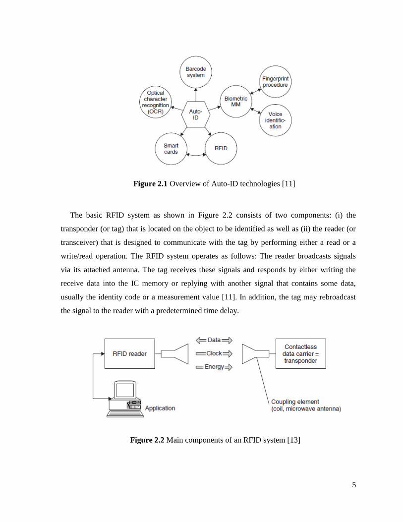
procedures as shown in the Figure 2.1.
5
Figure 2.1 Overview of Auto-ID technologies [11]
The basic RFID system as shown in Figure 2.2 consists of two components: (i) the
transponder (or tag) that is located on the object to be identified as well as (ii) the reader (or
transceiver) that is designed to communicate with the tag by performing either a read or a
write/read operation. The RFID system operates as follows: The reader broadcasts signals
via its attached antenna. The tag receives these signals and responds by either writing the
receive data into the IC memory or replying with another signal that contains some data,
usually the identity code or a measurement value [11]. In addition, the tag may rebroadcast
the signal to the reader with a predetermined time delay.
Figure 2.2 Main components of an RFID system [13]

6
The tag IC contains a unique identification of the object to be tracked. As this object
moves through the various processes such as manufacturing, warehousing, and
transportation, more data can be written on the attached tag IC. Therefore, data is stored and
can be retrieved and manipulated with minimal human intervention. This ease of data
manipulation and storage has made RFID technology very popular compared to other forms
of Auto ID technologies.
2.1.1 History of RFID
RFID technology can be traced back to as early as World War II, where British airplanes
were identified as a ‘friend of foe’ using this technology. Under the supervision of Scottish
physicist Sir Robert Alexander Watson-Watt, the British developed the first active identify
friend of foe (IFF) system [15]. A transmitter was installed on each British plane and the
radar-on-ground would be able to identify the plane based on the signal it received back
from the transmitter.
In 1948, Harry Stockman first showed how a communication link could be established
using reflected power [16], and in 1950 the first patent was lodged for passive transponders.
However, the optical barcode, a close rival of RFID, came to commercially usage in the
1960s and 1970s. In addition, the cheap implementation of optical barcodes made it a huge
success and is still prevalent in the most of the products today (2012). However, due to the
increased complexity and volume of business caused the industry to look for alternatives to
the barcode and hence started the journey for RFID.
Until 1979, RFID research was confined to laboratory experiments only. However, the
first commercial use of RFID was in animal tracking in the United States in the early 1980s.
This was followed by the first motor toll collection using RFID in Norway in 1987 and then
in US rail cars in 1994 [14]. In 1999, the Auto-ID center was established at the
Massachusetts Institute of Technology (M.I.T.) to research and develop worldwide protocols
and standards for RFID technology.
Absence of related technologies and global standards restricted the initial development of
this technology. Different countries and even different companies used RFID as proprietary
technology. There was minimal interoperability among different players. This problem was
addressed by UCC (Uniform Code Council) together with EAN (European Article

7
Numbering) create EPCglobal to commercialize EPC (Electronic Product Code) technology
[4]. EPCglobal ratified a second generation standard Gen2 in 2005, for broad adoption of
RFID [8]. This revolutionized the RFID industry creating numerous demands from industry
giants like Wal-Mart, US Department of Defense, Gillete, and so on.
2.1.2 Overview of RFID Technology
RFID system is a multidisciplinary system that can provide a complete solution and be
deployed independently or in compatibility with other existing systems such as the optical
barcode [11]. The basic goal of RFID is to make operations more accurate and user friendly
for businesses. This includes better quality control, automated tracking and product loss
prevention. As seen in Figure 2.3, the RFID system is divided into two layers: physical layer
and the IT layer [11]. The physical layer comprises tag, reader and the interrogation zone
(IZ).
Figure 2.3 RFID system divided into layers [11]
Tag: Tags are similar in purpose to optical barcodes, which are attached to objects and store
unique identification of the object/product. The tags primarily consist of two components:
the tag antenna and the IC chip. The tag antenna communicates with the reader by means of
electromagnetic waves. Based on the type of tag (active, passive, semi-passive or semi-
active) energy to turn-on the IC may be either acquired from the environment (reader RF
8
signal) or via an onboard battery supply. The IC chip stores the unique identification of the
system like product description, product code, product origin, etc. In unique tags sensors
might be attached on the tag to monitor environmental conditions such as temperature,
humidity, etc.
Reader: The reader is a device that is used to communicate with tags that are affixed onto
products. They usually are handheld, mobile, or stationary. Readers are made up of two
components: the antenna and the reader circuitry. The antenna communicates with the tag
using electromagnetic waves. Based on the application of use, the reader circuitry is
responsible for sending data through the reader antenna as well receiving data and
processing/storing it in the back end.
Interrogation Zone (IZ): The interrogation zone is an area where the reader is able to
read/write data to or from a tag. This area is a three-dimensional space in the vicinity of the
tag and the reader where electromagnetic waves can travel. The IZ is included in the physical
layer because the tag-reader communication link is influenced by the surrounding
environment that includes, interferences caused by other objects in the present in the IZ,
reflection of waves, etc.
The IT layer comprises the middleware and enterprise applications.
Middleware: The middleware is responsible for collecting data from the interrogator,
storing the data and sending it to the enterprise application. It also consists of software that
monitors, configures and manages the hardware of the reader.
Enterprise Application: Data is collected by the middleware by this application for
business processes like the creation of invoices.
RFID processes are geared to be application specific depending on the nature of the
business process. As a result, the process requires different combinations of readers and tags.
For example, applications criteria could involve read range, frequency protocol, form factors
(shape and size of tags) etc. Therefore, the RFID process is unique and its components have
to be carefully selected to meet specific application requirements. Other issues involve
standards and regulations. For standard EPCglobal was created, as a worldwide RFID
standard. The regulations are region specific such as FCC (USA), ERO (Europe), ACA
(Australia) etc. It is the responsibility of the RFID manufactures to comply with these

9
regulations when developing their products. In addition, mandates provided by some big
companies like Wal-Mart also need to be adhered to while developing the RFID products.
2.1.3 RFID Technology Applications
The areas of application of RFID are very vast and are projected to cover every single
item in the future [11]. Some broad areas where RFID is used in large volumes are
manufacturing, logistics, supply chain and tracking [3, 12]. These include healthcare,
pharmaceutical, livestock, baggage handling, access control, contactless payments, etc. To
make the concept of RFID application clear, two examples from manufacturing and supply
chain process are mentioned below.
Manufacturing: manufactures send their products to the shipping yard for transportations.
At the manufacturer’s end each item is tracked and placed into a box and then a pallet. The
boxes and pallets also are tracked and information about the quantity of the products is
stored.
Supply-Chain: At the yard, the items are read and information such as time, place and date
etc. are stored on a database. This data is available for manufacturers as well as supply-chain
companies like Fedex, UPS to track items and account for any losses or theft.
In this way the items are tracked and any lost or stolen items can be reported immediately
with information such as date, time, place where the items went missing. The manufacturers
also track the products throughout the supply chain process until they reach the customer. In
this way quality control is maintained.
2.1.4 Benefits of RFID
Although the RFID technology has become very popular in recent years, the main rival
optical barcode is still prevalent today. This is largely due to the fact that barcodes have the
competitive advantage of a cheaper technology to employ for business processes. However,
RFID is gaining steam, and with the reduction in the costs of RFID components (tags,
readers, ICs) the gap is narrowing. Some of the advantages and disadvantages of RFID
technology when compared to barcodes is mentioned in the Table 2.1 below.

10
Table 2.1 RFID technology compared to traditional barcodes [1].
RFID Barcode
1. No line of sight (LOC) required. Tags
may have any orientation.
1. LOC required or else to scan item for
data.
2. Identification of items, cases and pallets is
possible.
2. Only one category (items, pallets)
identification.
3. Simultaneous identification (read//write)
possible.
3. Only one item can be scanned at a time.
4. High data capacity (16-64 Kilobytes). 4. Low data capacity (1-100 bytes).
5. High read distance (0-5m). 5. Lower reading distance (0-50cm).
6. Wear and tear has minimal influence. 6. If barcode ink is smudged then, it is
impossible to scan the item.
7. Cost of tag is high ($0.15+) 7. Barcode can be printing on item,
minimal costs.
8. RFID tags are application specific so
require time to create specific tags to meet
requirement.
8. Barcode can be printed on items almost
immediately.
2.1.5 RFID Antenna Characteristics
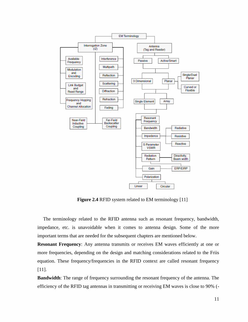
There is a lot of terminology associated with RFID technology from the perspective of
electromagnetic (EM) waves. The EM waves are essentially composed of mutually
interchanging electric and magnetic fields that are perpendicular to each other as well as the
direction of propagation [11]. As these EM waves propagate, they radiate energy in the three
dimensional space surrounding them. Therefore, as the waves travel further away from the
source the radiated power density decreases in magnitude. The terminology seen throughout
the RFID system is shown in Figure 2.4 [11].
11
Figure 2.4 RFID system related to EM terminology [11]
The terminology related to the RFID antenna such as resonant frequency, bandwidth,
impedance, etc. is unavoidable when it comes to antenna design. Some of the more
important terms that are needed for the subsequent chapters are mentioned below.
Resonant Frequency: Any antenna transmits or receives EM waves efficiently at one or
more frequencies, depending on the design and matching considerations related to the Friis
equation. These frequency/frequencies in the RFID context are called resonant frequency
[11].
Bandwidth: The range of frequency surrounding the resonant frequency of the antenna. The
efficiency of the RFID tag antennas in transmitting or receiving EM waves is close to 90% (-

12
10dB) and this is known as the bandwidth for the RFID system [11]. This is typical for RFID
system antennas, but may differ for antennas for different technologies.
Impedance: The impedance is divided into three resistances namely, radiative, resistive, and
reactive. Power absorbed by the radiative resistance is transmitted as EM energy or vice
versa. The radiative resistance is directly proportional to the antenna length. The resistive
radiation just dissipates power absorbed in the form of heat. The reactive resistances act as
barriers and inhibit the transfer of energy. These are typically capacitive or inductive and at
resonant frequency cancel out each other, hence the antenna can freely radiate energy
efficiently at the resonant frequency.
Radiation Pattern: For any antenna the radiation pattern is never spherical [11]. In the
RFID context, reader antennas have a directional radiation pattern (all the energy is beamed
into one direction) and the tag antennas have a toroid shaped pattern (they can be read from
all direction).
Polarization: This is a very important concept to grasp. The EM waves radiated from the
antenna have an electric and magnetic field that are perpendicular to each other. Based on
the orientation of the electric field, the polarization of the antenna may be linear or circular.
In the RFID context, readers are typically circularly polarized whereas tags are linearly
polarized. Furthermore, the circular polarization allows the reader to be compatible with any
linearly polarized tag thereby reducing costs associated with polarization mismatch. This
polarization mismatch causes only half the power to be received by the tag antenna, a 3dB
loss. The term that describes the amount of power lost due to mismatch is called polarization
loss factor (PLF). The PLF ranges from 0 to 1, where 0 indicates no transfer or power and 1
represents maximum power transfer as seen in table 2.2 for different polarizations.
Table 2.2 Effect of polarization mismatch resulting in different values for PLF [19].
Incident Wave Polarization
(Transmit Antenna)
Receive Antenna
Polarization
PLF
Vertical Linear Vertical Linear 1
Linear (V or H) Circular (RH or LH) 0.5
Vertical Linear Horizontal Linear 0
RH Circular RH Circular 1
RH Circular LH Circular 0

13
2.1.6 RFID Tags
RFID tags are required in large quantities as they have to be attached to all the products
that need to be tracked. The main components of the RFID tags are the antenna and the
integrated circuit (IC) chip. The other components include the dielectric substrate,
packaging, etc. and will be discussed in this section.
2.1.6.1 Tag IC
This is a semiconductor-based circuitry that is designed by a chip manufacturer (Texas
Instruments, NXP Semiconductors, etc). The tag manufacturers buy these ICs based on the
application requirements. The IC is divided in to three parts:
Analog front end: this part is responsible for controlling the power. The power may be
supplied by either the battery or external EM radiation. The analog front end part consists of
components such as voltage regulators, modulators, clock cycle generators, and so on.
Detection, Encoding/Decoding unit: This unit is responsible for the modulation and
demodulation of signals and encoding the received signal into bits to be stored to the
memory unit of the IC.
Memory unit: The memory is divided into blocks which may be either read only or
read/write enables depending on the application. The unique identification code, error
checking codes, passwords, etc. are stored in the IC memory [11].
2.1.6.2 Substrate
The substrate is a dielectric material and forms the base of the RFID tag. The conductive
material (copper, aluminum) is etched on top of the substrate and the IC is attached to either
ends of the conductor. The substrates are usually used are thin, flexible and can stand harsh
environmental conditions. Some commonly used materials for RFID substrates are PVC,
PET, FR-4, Rogers Duriod, etc.
2.1.6.3 Tag Packaging
After the tag has been manufactured it is important to make sure that the tag is packaged
properly in order to protect it from the physical environment. Some important tag packaging
terms are mentioned below.

14
Strap: In cases where the IC pads are small, two pads are provided by the manufacturer to
help attach the IC to the antenna. This is called the strap.
Inlay: The strap when added to the antenna with some additional substrate is called the
inlay. These inlays are typically produced by label makers with the help of an RFID printer.
Smart Label: The inlay is inserted inside a paper label. The paper label has readable
information printed outside it like a barcode, the EPC logo, etc. This is called a smart label.
Encapsulated tag: In some applications (supply chain process) the tag need to be protected
from the physical environment from damage. In such cases the tags are encapsulated in hard
RF translucent outer covers such as polypropylene, polyacetate, etc [11]. This protects the
tag from damage.
2.1.6.4 Tag Classification
Tags are separated into different categories based on criteria such as power source,
frequency of operation, protocols, functionality, etc. An overview of the RFID tag
classification in shown in Figure 2.5 [11] and some of these criteria will be explained in the
following sections.
Figure 2.5 RFID tag classification [11]

15
2.1.6.5 Power Source
Since tags depend on a power source for operation they can be divided into four classes:
semi-active, active, semi-passive, and passive [13].
Active-tags: use battery power for powering the logic and communications link. As a result,
these tags have greater read-range when compared to passive or semi-active tags. Active tags
have the disadvantage of relying on a battery source, which once depleted must be replaced.
Semi-passive tags: use batteries to power only the logic part of the tag once the tag is
activated through incident energy from the reader. The semi-passive tag modulates the
incident signal to communicate with the reader. The process of reflecting the energy back to
the reader as a means of communication is called back scattering [12].
Semi-active tags: harvest energy from their environment to power the logic and
communications link. These tags can use solar energy, vibration energy (piezoelectric
rectification) or another means to power the logic on the tag. They are also known as energy
harvesting
Passive tags: do not have any source of power such as batteries and rely solely on the power
that is rectified by the reader to power the tag. Like semi-passive tags, these tags also use the
back-scattering process to communicate with the reader. Semi-passive and passive tags can
be distinguished through their coupling mechanism: near-field and far field operation [13].
Table 2.3 RFID Tag Types based on power source
Active Tag
Communication and logic powered by
onboard battery.
Increased range
Semi-Active Tag
Logic powered by onboard battery
Communications enabled by back
scattering incident signal.
Semi-Passive Tag
Logic powered by energy harvesting
methods (solar, vibration, etc)
Communications enabled by back
scattering.
Passive Tag
No on-board battery, relies on RF waves
emitted by the reader to power logic
Communications enabled by back
scattering.
16
2.1.6.6 Frequency of Operation
There are several frequency bands of operation for the RFID tags namely, low frequency
125-134 kHz (LF), high frequency 13.56 MHz (HF), ultra high frequency 400-960 MHz
(UHF), and microwave 2.4 GHz and 5.8 GHz [2],[3] and [11]. The operation of frequency
for RFID is regulated by each country. For example, the UHF RFID frequency in North
America is 915 MHz but for most of Europe it is 860 MHz. Furthermore, RFID tags are
designed to meet these frequency specification based on the application such as short read
range, long read range, enhanced security, better data transfer rate, etc.
Low frequency tags (125-134 kHz): were among the first tags to be deployed for RFID
applications. The main advantage of these tags was that they could be read while attached to
objects containing water, animal tissues, metal, wood, and liquids [11]. However, the LF
tags had several drawbacks such as use in close proximity applications, only a short read
range of a few centimeters, very low data storage capacity and no anti-collision measures
which are necessary if the reader requires to be read multiple tags simultaneously.
High frequency tags (13.56 MHz): are currently the most widely used in the RFID
industry. The HF tags use inductive coupling as a source of power to communicate with the
readers [11]. These tags have several advantages such as better read range, typically half a
meter, high data storage capacity, good anti-collision measures for readers to communicate
with multiple tags. All these features make HF tags an ideal choice for applications such as
credit cards, library book tags, airline baggage tags and asset tracking [11].
Ultra high frequency tags (433 MHz and 860-960 MHz): use far-field coupling or back
scatter coupling to communicate with each other [11]. These UHF tags have several
advantages such as good memory size for the data, up to 240 bits, and very long read range,
typically 20 meters under good conditions. However, the main disadvantage of UHF tags is
that their performance is severely degraded when attached to objects containing water,
biological tissues and metals. Some typical applications of the UHF tags include supply
chain, inventory and logistics, apparel and aviation baggage.
Microwave tags (2.4GHz and 5.8GHz): have high data transfer rate that allow
communication between devices at a very high rate [11]. Consequently, the microwave tags
are most suited for application where real-time asset tracking is required. The main
drawback of the microwave tag is higher cost to develop and most of the tags are active tags

17
i.e. they require an external battery to power the microchip on the tag. Typical applications
include highway toll collection, real-time location system, etc.
2.1.6.7 Functionality (EPC Global Classes)
EPCGlobal (RFID standardization body) has classified RFID tags into six different
classes based on the certain criteria such as power, memory capacity, protocols, etc [3], [13],
[11] and [16]. These classes are mentioned in the Table 2.4 below.
Table 2.4 RFID classes and their functionality
Class Functionality
0 Passive tags that have ‘write once read many’ (WORM) IC chips.
The data is written when the IC is manufactured.
1 Passive tags with WORM chips. The data is either written during
chip manufacturer or by the customer before use.
2 Passive tags with read/write capability. The user can add additional
information to the tag for encryption.
3 Semi-passive tags with on-board sensors. Have read/write
capability and additional memory space available for use.
4 Active tags with on-board sensors. Have read/write capability. User
memory. Peer communication provision with similar active tags
and readers.
5 This class defines readers. These readers can communicate and
power tags in the aforementioned classes [0 - 4].
2.1.6.8 Protocols
Protocols are a given set of codes (‘language’) that allow communication between the tag
and the reader. There also exist protocols where a reader can communicate with other
readers in close vicinity.

18
Protocols are divided into the following categories:
Open Protocols: These are developed by standardization bodies such as ISO 18000-6(A/B),
ISO 14443 (A/B), etc. Open protocols are available globally and can be used by anyone.
Proprietary Protocols: These are developed by manufacturers for their own business such
as Texas Instrument’s ‘TI Tag-IT’, Intermec’s IntelliTag, etc.
The protocols mentioned above can be divided into sub sections where the readers might
need to use multiple protocols to for different tags. These types of protocols are mentioned
below:
Air Interface Protocols: These protocols depend on how the tag and reader communicate
based on frequency of operation, bit rate, modulation, anti-collision algorithms, etc.
Data Content Protocols: These protocols define the layout of the memory structure in the
IC. Therefore, these protocols make it easier to locate specific data on the tag’s IC.
2.1.6.9 Tag Antenna
In UHF tags, the antennas preferred are usually a dipole or patch structures [11]. The
main considerations while choosing the antenna for design are mentioned below.
Must be small enough to attach on to object (typically 50.8mm x 101.6 mm) [10].
Have an omnidirectional radiation pattern so that the tag can be read from any
direction.
Must have minimum turn-on impedance for the tag-IC.
Avoid polarization mismatch (discussed in section 2.1.5)
Be very robust and cheap.
2.2 RF in RFID
This section starts with the discussion of antenna fundamentals such as field regions,
dipole radiation patterns. The second part of this sections deals with coupling mechanisms
such as inductive coupling, or modulated back-scatter coupling.
19
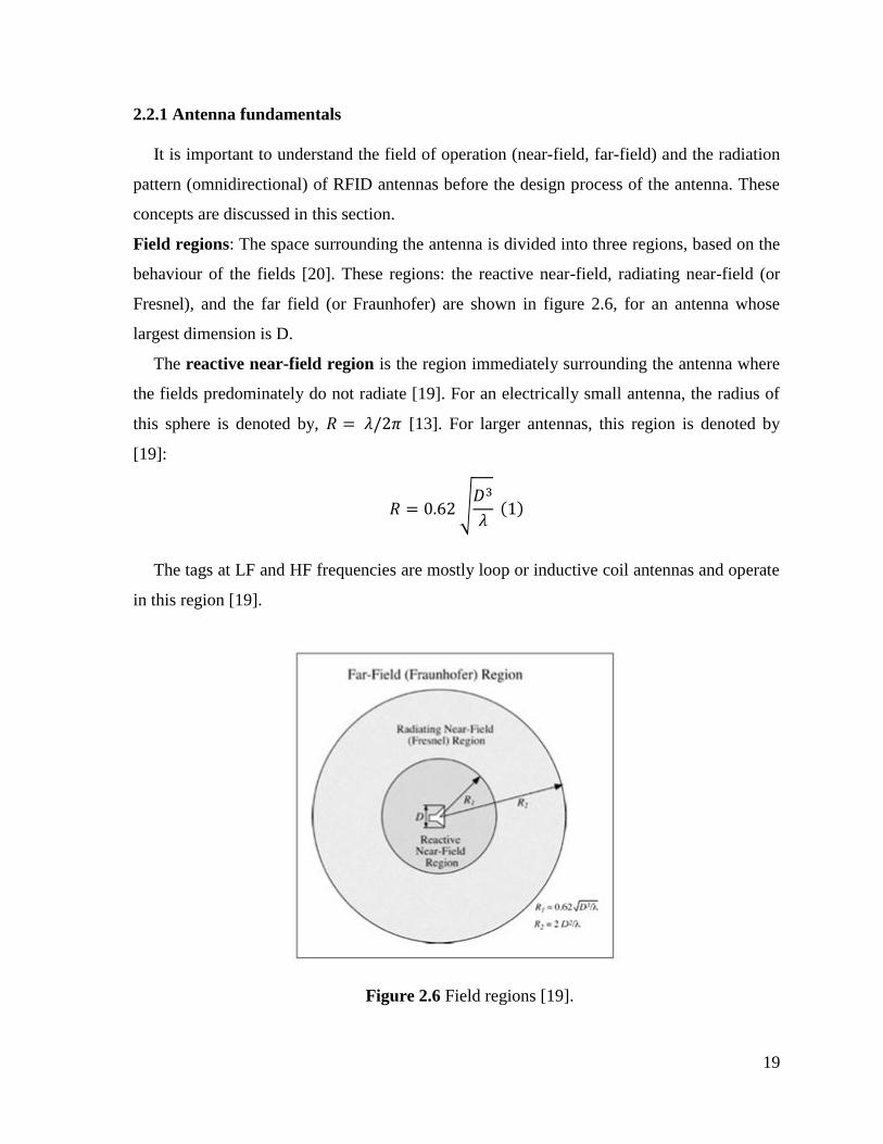
2.2.1 Antenna fundamentals
It is important to understand the field of operation (near-field, far-field) and the radiation
pattern (omnidirectional) of RFID antennas before the design process of the antenna. These
concepts are discussed in this section.
Field regions: The space surrounding the antenna is divided into three regions, based on the
behaviour of the fields [20]. These regions: the reactive near-field, radiating near-field (or
Fresnel), and the far field (or Fraunhofer) are shown in figure 2.6, for an antenna whose
largest dimension is D.
The reactive near-field region is the region immediately surrounding the antenna where
the fields predominately do not radiate [19]. For an electrically small antenna, the radius of
this sphere is denoted by, [13]. For larger antennas, this region is denoted by
[19]:
√
( )
The tags at LF and HF frequencies are mostly loop or inductive coil antennas and operate
in this region [19].
Figure 2.6 Field regions [19].

20
The radiating near field, or Fresnel region, lies between the reactive near-field region
and the far-field region. In this region the fields are predominately radiating, and the angular
field distribution depends on the distance from the antenna [19]. If the antenna is small this
region may not exist [19]. For larger antennas, the inner radius of this spherical region is
given by (1) while the outer region is given by [19]:
( )
The far-field, or Fraunhofer, region is the region where the fields are radiating and their
angular variation is essentially independent of the distance from the antenna, and the fields
components lie essentially in the transverse plane to the direction of propagation [19]. The
traveling waves dominate in this region where the decay rate is (where r is the distance
from the antenna to the observation point in the far-field region) [19]. These traveling waves
carry the electromagnetic power to the passive and semi-passive UHF and microwave
transponders [19].
Radiation Pattern: An accurate model for the dipole is quite complex, but forming a
reasonable approximation for the radiation of the dipole is simple. We can achieve this by
looking at small segments of a dipole. For each segment we assume that the current is
uniform. The dipoles examined here known as Hertzian dipoles. As seen in figure 2.7a, the
distance R from a point z' on the dipole to the observation point P is given by :
√ ( ) ( )
In the far-field region of the dipole (where R > 2l2/λ), as shown in figure 2.7b, the
following approximations can be made for determining the radiated patterns:
R ≈ r, for amplitude terms
R ≈ r – z’cosθ, for phase terms
Since the length of the wire is so small, the electric current (I) along the wire is assumed
to be constant and flowing solely in the z-direction :
( ) ( )

21
l is the length of the dipole, P is the observation point (typically more than a wavelength
away).
Figure 2.7 Far field approximation of R for a finite length dipole [19]

22
Normalized radiation patterns of the dipole of various lengths [18] are shown in Figure
2.8. As the length of the antenna increases, the beam narrows and the directivity increases.
When the length of the dipole exceeds a wavelength, additional lobes will appear in the
radiation pattern.
Figure 2.8 Radiation pattern of dipole of various lengths [18]
The intensity of the electric field is given by [19].
( ) (5)
In the above equation, j2
= -1,ε0 is the free space permittivity, c is the speed of light, k =
2π / λ and ω = 2πf

23
Two important points observed from the above equation are
(1) The power intensity is the square of the E-field intensity, and the E-field power
drops off as 1/d, and this makes the power drop off as 1/d2.
(2) The E-field intensity falls off with θ as sin θ, resulting in a radiation pattern that
looks like a toroid-like or ‘donut-shaped’ pattern.
The half-wave dipole does not have a uniform current distribution over its length. At
resonance, it is a half sine wave. The bottom line is that the dipole radiation is at maximum
in the broadside direction, and essentially goes to zero in the direction of the poles.
2.2.2 Coupling Mechanisms
The coupling mechanisms of different classes of tags are important when it comes to the
operation characteristics such as reading distance and operating power. The coupling
mechanisms related to RFID tags can be divided into two categories namely, near-field
coupling (inductive coupling) and far-field coupling (modulated back-scattering). This
section will discuss these types of coupling mechanisms.
Near field coupling: This is the three dimensional space immediately surrounding the
antenna. Low frequency (LF), High frequency (HF) tags and Near Field Communication
(NFC) tags use this type of coupling mechanism. The antenna used for this type of coupling
is referred to as a ‘transformer’ [15] and has an ‘inductive coil’ shape. Since the reading
distance is limited to a few centimeters the typical applications for this type of coupling
include, animal tagging, proximity cards, contactless payments, etc. The inductive coupling
operation between the reader and the tag/transponder is shown in the figure 2.9.
Far-field coupling: This is the three-dimensional space beyond the near field and
encompasses the reader as well as the tag. The electromagnetic energy is radiated in a radial
manner in the far field with the power dropping off with increasing distance. The EM energy
radiated by the reader’s antenna is reflected or absorbed by the tag’s antenna based on the
tag antenna’s radar cross section (RCS). The tag’s IC switches between a load and
open/short circuit and thus is able to control the reflected EM wave. The reflected EM wave
is picked up by the reader’s antenna, is amplified and decoded to extracts the sent data. This
type of coupling is used in ultra high frequency (UHF) tags and microwave tags. Since the

24
reading distance is several meters (20 meters, [19]) the typical applications for this type of
coupling include, supply chain processes, pharmaceutical, healthcare, etc. The modulated
backscatter operation between the reader and the tag/transponder is shown in the figure 2.10.
Figure 2.9 Power supply to an inductively coupled tag from magnetic alternating field
generated by the reader [11]
2.3 Chapter Summary
In this chapter we discussed the history and the fundamentals of RFID technology (RFID
tags, tag antenna theory, coupling mechanisms, etc). The different classes of RFID tags
based on their criteria such as power, protocols, frequency of operation were discussed. In
the second part, antenna theory fundamentals and tag-reader coupling mechanisms
(communication links) were mentioned briefly. The chapter aims to give its reader an overall
view of the RFID technology with emphasis on RFID tags.

25
Figure 2.10 Modulated backscatter by modulation of the transponder impedance ZT (=RT)
[19]

26
CHAPTER 3 – RFID tag antenna design requirements and testing procedures
The design requirements for a passive RFID tag antenna have been extensively
investigated [4]-[6], [10] and [21]. The first step involves understanding tag performance
criteria such as increased read-range, orientation sensitivity, reduced environmental impacts
(humidity, metals) etc. Secondly, the passive RFID design process as suggested by [5]
should be addressed which includes antenna-chip impedance matching and read range
measurement. Finally, the tag antenna impedance itself (excluding the chip) needs to be
tested using the measurement setup as proposed by [21].
In this chapter we will discuss the RFID tag antenna design requirements and the test
procedures. It comprises of three parts; the first part introduces different tag performance
criteria. The second part highlights the design process which includes optimization, analysis
and prototype construction. The last section deals with the testing procedures that include
antenna measurement setup (vector network analyzer) and reading-range setup (anechoic
chamber).
3.1 Tag Performance Criteria
Although there are many different tag performance criteria such as tag orientation
sensitivity, chip sensitivity, frequency of operation, etc. the most important one is read
range. The tag read range is defined as the maximum distance at which the RFID reader can
detect the RFID tag. The reader has a higher sensitivity than the tag and as a result the read
range can be considered as the tag response threshold. Furthermore, the read range is also
dependant on other factors such as tag orientation and environmental losses [5]. The read
range is calculated using the Friis free-space equation (6) shown below [5].
√
( )

27
In equation (6), is the wavelength, is the power transmitted by the reader, is the
gain of the transmitting antenna, is the gain of the tag antenna, is the minimum
threshold power necessary to turn on the chip and is the power transmission coefficient.
It is given by
| | ( )
In the equation (7) above, represents the chip impedance ( ) and represents
the antenna impedance ( ) (Figure 3.1). In addition, when maximum power is
transferred and the antenna is said to be perfectly matched to the chip impedance at a
particular frequency. However, if then, the antenna is not matched to chip impedance
at all. Typically for RFID tags, impedance matching deteriorates when [23]. In
addition, good impedance matching for RFID tags is considered only when [5].
Figure 3.1 Antenna impedance, chip impedance and read range as functions of frequency for
a typical RFID tag [5].

28
The figure 3.1 illustrates the qualitative behavior of the antenna impedance, chip
impedance and the read range for a typical RFID tag at a given frequency. The frequency of
peak range is defined as the tag resonance. In addition, the range bandwidth shown in figure
3.1 is defined as the frequency band in which the tag offers acceptable minimum read range.
From (6) we conclude that is frequency dependant and determines the tag resonance.
Another important concept as indicated in figure 3.2 is the tag performance chart [5]. This
chart helps the designer to estimate the range tradeoff between the impedance matching and
the gain. Basically, the range in (6) is normalized by a factor as shown in (8). This factor
is the range of the tag with 0 dBi antenna perfectly matched ( ) to the chip impedance at
a fixed frequency.
√
( )
Figure 3.2 Tag performance chart: contours of the constant normalized range in the gain-
transmission coefficient plane [5].

29
The antenna designer realizes that the design process involves tradeoffs between antenna
gain, impedance and bandwidth. The figure 3.2 is one such tool that the antenna designer can
use to determine the requirements for a ‘good tag’ based on the read range.
Other important tag performance criteria such as chip sensitivity, orientation sensitivity,
etc. are mentioned below.
Chip Sensitivity: Chip sensitivity threshold (Pth) is an important tag limitation. It is the
minimum received RF power to turn on the RFID chip. The lower it is, the longer the
distance at which the tag can be detected. Chip sensitivity is usually determined in the RF
front end architecture and fabrication process [4].
Orientation Sensitivity: The EM waves radiated from the antenna have an electric and
magnetic field that are perpendicular to each other. Based on the orientation of the electric
field, the polarization of the antenna may be linear or circular. In the RFID context, readers
are typically circularly polarized whereas tags are linearly polarized. This polarization
mismatch causes only half the power to be received by the tag antenna, a 3dB loss.
Environmental Limitations: The antenna designed for an RFID chip using computer
simulations, or even through measurements may work very well in theory. However, in
practice, there are several environmental factors that degrade the tag performance.
Environmental issues that will degrade tag performance like placing the tag near a plastic
bin, on a cardboard box, on a bottle of water, or even near metals are hard to assess. Typical
ways to mitigate these effects are placing foam separators between the tag and the
environment (water, metal, etc) [10].
3.2 Tag Design Process
In this section the RFID tag antenna design process will be mentioned briefly. The overall
chain of steps to follow in the successful realization of the RFID tag is illustrated in figure
3.3 which is self-explanatory. However, each section from the figure 3.3 will be briefly
addressed for clarity.
1. Select application and define tag requirements: this is perhaps the most important
step. The designer needs to determine beforehand several tag requirements such as
frequency band (915 MHz or 868 MHz), tag size, maximum read range, operation
environment (metals, water, etc), orientation (polarization of tag), costs (printed ink,
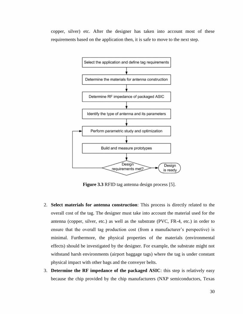
30
copper, silver) etc. After the designer has taken into account most of these
requirements based on the application then, it is safe to move to the next step.
Figure 3.3 RFID tag antenna design process [5].
2. Select materials for antenna construction: This process is directly related to the
overall cost of the tag. The designer must take into account the material used for the
antenna (copper, silver, etc.) as well as the substrate (PVC, FR-4, etc.) in order to
ensure that the overall tag production cost (from a manufacturer’s perspective) is
minimal. Furthermore, the physical properties of the materials (environmental
effects) should be investigated by the designer. For example, the substrate might not
withstand harsh environments (airport baggage tags) where the tag is under constant
physical impact with other bags and the conveyer belts.
3. Determine the RF impedance of the packaged ASIC: this step is relatively easy
because the chip provided by the chip manufacturers (NXP semiconductors, Texas

31
instruments, etc) usually come with the datasheet which includes chip impedance
values. The designer in most cases trusts this chip impedance value because to
measure the exact chip impedance requires further measurement setups and increases
the overall cost.
4. Identify the type of antenna and its parameters: this step is important because
there is a range of antenna shapes and sizes that designers use for RFID tags such as
meandered dipole, folded dipole, capacitive-tip loaded dipole, inverted-F … [7],
[24]-[26]. Thus, the designer needs to know how the antenna shapes effect the overall
tag performance.
5. Perform parametric study and optimization: this step usually involves analyzing
the tag antennas with electromagnetic (EM) modeling and simulation tools such as
method of moments (MoM), finite-element method (FEM) or finite-difference time-
domain (FDTD) method. Fast EM analysis tools such as Ansoft HFSS are very
important for efficient tag design. For example, the geometrical parameters (height,
width) of a meandered dipole antenna designed using HFSS can be investigated to
see how incremental changes effect tag performance (impedance, frequency, etc).
6. Build and measure prototypes: this is last stage in the design process. The antennas
fabricated based on simulation results need to be verified for impedance matching
using a vector network analyzer and read range measurement in an anechoic
chamber. If the results are in close agreement with the simulation results then, the
design is ready. Otherwise, the designer needs to go back to step 5 and modify the
simulation setup.
3.3 Tag Testing Procedures
The testing procedures for fabricated RFID tags are mentioned in this section. These
testing procedures include 1) read range and 2) impedance measurement as mentioned
below.
Read range: range measurement for RFID tags is usually carried out in a controlled
environment such as an anechoic chamber as shown in Figure 3.4 [5]. The tag is placed at a
fixed distance from the reader. At each frequency, the minimum power Pmin, needed to
communicate with the tag is recorded. Since the loss L of the connecting coaxial cable, the

32
gain of the transmitting antenna Gt, the distance d to the tag are known, the tag range for any
transmitter EIRP (effective isolated radiated power) can be determined from (9).
√
( )
Figure 3.4 RFID tag range measurement using anechoic chamber [5].
Some other general guidelines for selecting tag position using the anechoic chamber setup
[5] are listed below.
1. The distance must be such that the tag will respond in the far-field region.
2. The tag must be placed in the quiet zone of the chamber where multipath is minimal.
Impedance measurement: most RFID tags are balanced dipoles [22] and this makes it
harder to measure the electrically small antennas directly using a vector network analyzer
(VNA). To overcome this problem as suggested by [22], only half of the antenna structure is
placed on a metal plate as shown in Figure 3.5 and Figure 3.6.
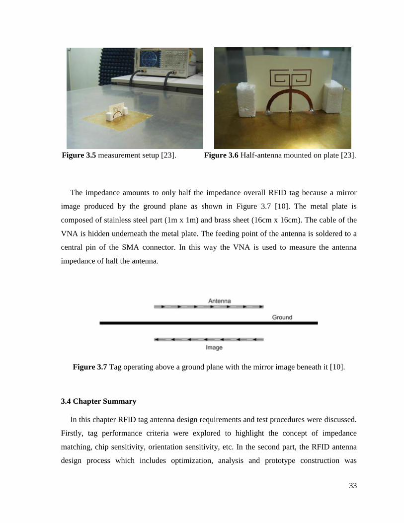
33
Figure 3.5 measurement setup [23]. Figure 3.6 Half-antenna mounted on plate [23].
The impedance amounts to only half the impedance overall RFID tag because a mirror
image produced by the ground plane as shown in Figure 3.7 [10]. The metal plate is
composed of stainless steel part (1m x 1m) and brass sheet (16cm x 16cm). The cable of the
VNA is hidden underneath the metal plate. The feeding point of the antenna is soldered to a
central pin of the SMA connector. In this way the VNA is used to measure the antenna
impedance of half the antenna.
Figure 3.7 Tag operating above a ground plane with the mirror image beneath it [10].
3.4 Chapter Summary
In this chapter RFID tag antenna design requirements and test procedures were discussed.
Firstly, tag performance criteria were explored to highlight the concept of impedance
matching, chip sensitivity, orientation sensitivity, etc. In the second part, the RFID antenna
design process which includes optimization, analysis and prototype construction was

34
discussed. Finally, the testing procedures for read range and impedance were explored. The
RFID tag antenna design process is not a simple process because it requires extensive
knowledge of antenna theory as well as the results published by other researchers [4], [7],
and [10].

35
Chapter 4 - Conjugate Impedance Matching Techniques
This chapter presents different design methodologies of UHF (915 MHz) RFID passive
tag elements. As already mentioned, passive tags require RF energy supplied by the reader’s
antenna to power the microchip. Passive ICs are generally highly capacitive because of the
necessary power required to bias the IC which is drawn through electromagnetic coupling
[3]. As a result, the antennas designed should exhibit a low resistance value and a high
inductance value to match the input impedance of the tag IC. Note the impedance value of
the IC corresponds to the ‘turn-on’ impedance of the IC. These values are provided by the IC
manufacturer.
The HFSS design tool [27], based on Finite Element Method (FEM), is used to analyze
and optimize the antenna design. The FEM is a numerical technique used to solve Boundary
Value Problems (BVP’s) governed by a differential equation and a set of boundary
conditions [28]. In this chapter, T-Match (165mm x 20mm), inductively coupled loop
(165mm x 35mm) and nested-slot (163mm x 163mm) antennas were designed to achieve
maximum read range.
4.1 T-Match
The equivalent circuit of a T-match structure is shown in Figure 4.1. The input impedance
of a planar dipole of length l can be changed by using a short circuit stub as explained in
detail in section 9.7.3 of [19]. The antenna source is connected to the second dipole of length
a< l and placed at a distance b from the larger dipole. The electric current distributes along
the two radiators according to the size.
The input impedance seen by the source is expressed in equation (10) below taken from
[7].
( )
( ) ( )

36
Figure 4.1 T-match of the planar dipole with its equivalent circuit [7].
ZA- is the dipole impedance taken in the centre in the absence of a T-match connection.
Zt, is the impedance of the short circuit stub and Zo is the characteristic impedance of the
two-conductor transmission line with spacing b. They are given by the following relations.
( )
(
√
) ( )
=0.25w and =8.25w’ are the equivalent radii of the dipole and the matching stub,
respectively. α = ln(b/re’)/ln(b/re) is the current division factor between the two conductors.
The geometrical parameters a, b and w’ can be adjusted in order to match the complex chip
impedance Zchip.
For half-wavelength dipoles, the T-match port is inductive and for smaller wavelength
dipoles this impedance can be both inductive and capacitive. Figure 4.2 [7] shows a
matching chart for the T-match layout where the ratio between the dipole’s cross section is
fixed to w/w’=3. The parameters a and b both influence the resistance and the reactance
values. Generally, high resistance values are found while using the classic T-match as shown
in Figure 4.1.2. Further degrees of freedom may be needed to overcome this problem. For
example, we may use multiple T-matches in a layout or use an embedded T-match feed as
shown in figure 4.3.
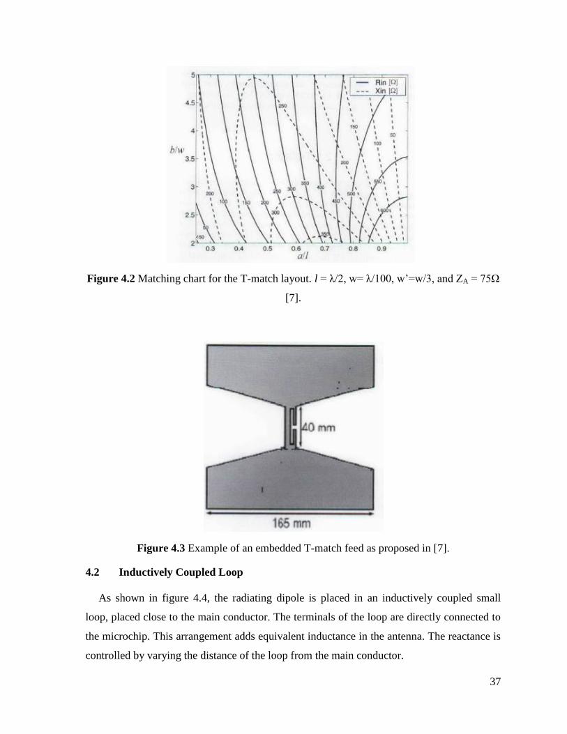
37
Figure 4.2 Matching chart for the T-match layout. l = λ/2, w= λ/100, w’=w/3, and ZA = 75Ω
[7].
Figure 4.3 Example of an embedded T-match feed as proposed in [7].
4.2 Inductively Coupled Loop
As shown in figure 4.4, the radiating dipole is placed in an inductively coupled small
loop, placed close to the main conductor. The terminals of the loop are directly connected to
the microchip. This arrangement adds equivalent inductance in the antenna. The reactance is
controlled by varying the distance of the loop from the main conductor.

38
Figure 4.4 Inductively coupled feed with its equivalent circuit [32]
The inductive coupling can be modeled by a transformer. The resulting impedance seen
from the loop’s terminals is given by [7].
( )
( )
In the above equation Zloop = j2πf Lloop is the loop’s input impedance. Whether the dipole
is at resonance or not, the total input impedance depends on the loop inductance, Lloop. The
resistance is related to the transformer mutual inductance M as shown below [7].
( ) ( )
( ) ( )
( ) ( ) ( )
In equations 14 and 15, RA represents the antenna’s resistive impedance, f0 is the resonant
frequency, M is the mutual inductance of the transformer and Lloop is the inductance of the
loop. The total input resistance is dependent on the loop’s shape and the dipole-loop
distance. Figure 4.5 shows the loop-driven dipole for a square loop (a = b). Input reactance is
unaffected by loop distance (d). For a fixed loop, the resistance reduces as the value of d

39
increases. Therefore, for design purposes, the loop size can first be setup to match the chip’s
reactance. After the reactance is set, the loop-dipole distance can be adjusted to control the
resistance.
Figure 4.5 Matching chart for the loop-fed dipole. l = λ/2, w= λ/100, w’=w/3 and a=b
(square loop) [7].
4.3 Nested Slot
This is a matching strategy useful for tags with large planar dipoles or suspended patches
as shown in Figure 4.6 [31]. The non-resonant slot has an inductive reactance, and this
makes it possible for complex impedance matching even when the tag is attached to a high
permittivity substrate as shown in Figure 4.8 [22]. The slot-line can be considered as
impedance transformer, where each discontinuity (tooth) provides energy for storage and
radiation. Increasing the number of teeth can help us miniaturize the design and achieve
multi-band features [32].
Maximum antenna gain is fixed by the patch length, l, and the impedance tuning can be
achieved by changing the slot dimensions a and b. Varying the shape and size of the internal
slot may cause the antenna to act as an H-slot, a broadband dipole or a doubly folded dipole.
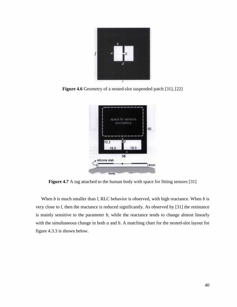
40
Figure 4.6 Geometry of a nested-slot suspended patch [31], [22]
Figure 4.7 A tag attached to the human body with space for fitting sensors [31]
When b is much smaller than l, RLC behavior is observed, with high reactance. When b is
very close to l, then the reactance is reduced significantly. As observed by [31] the resistance
is mainly sensitive to the parameter b, while the reactance tends to change almost linearly
with the simultaneous change in both a and b. A matching chart for the nested-slot layout for
figure 4.3.3 is shown below.

41
Figure 4.8 Matching chart for the nested-slot matching layout. l = λ/2, d = g = λ/150 [7]
4.4 HFSS Modified T-Match Simulation
4.4.1 T-Match Antenna Design
The antenna is made of copper metal with thickness, 0.02 mm. The substrate is made of
polyester with thickness, 0.1 mm (with εr = 3.2 and loss tangent δ = 0.003). Its dimensions
are width = 16.5 mm and length = 180 mm. The geometrical parameters of the antenna as
shown in Figure 4.4.1 are as follows:
l = 163 mm
a = 15 mm
b = 8 mm
w = 3mm
w’ = 1 mm
Port separation = 2 mm
The IC impedance used for this design at 915 MHz is equal to 12 – j140 Ω (Alien-Higgs).
That means that the load antenna impedance should be 12 + j140 Ω for maximum power
transfer (conjugate matching).

42
Figure 4.9 T-Match RFID antenna design layout.
Figure 4.10 T-Match configuration for planar dipoles [7].
4.4.2 T-Match Simulation Results
The results on the following page show the HFSS simulations results for the return loss
and the impedance.
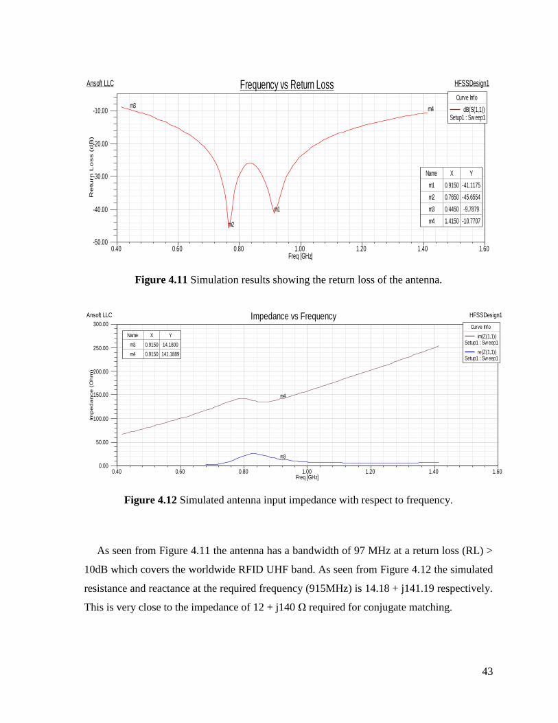
43
Figure 4.11 Simulation results showing the return loss of the antenna.
Figure 4.12 Simulated antenna input impedance with respect to frequency.
As seen from Figure 4.11 the antenna has a bandwidth of 97 MHz at a return loss (RL) >
10dB which covers the worldwide RFID UHF band. As seen from Figure 4.12 the simulated
resistance and reactance at the required frequency (915MHz) is 14.18 + j141.19 respectively.
This is very close to the impedance of 12 + j140 Ω required for conjugate matching.
0.40 0.60 0.80 1.00 1.20 1.40 1.60Freq [GHz]
-50.00
-40.00
-30.00
-20.00
-10.00
Re
turn
Lo
ss (
dB
)
Ansoft LLC HFSSDesign1Frequency vs Return Loss
m1
m2
m3 m4
Curve Info
dB(S(1,1))Setup1 : Sw eep1
Name X Y
m1 0.9150 -41.1175
m2 0.7650 -45.6554
m3 0.4450 -9.7879
m4 1.4150 -10.7707
0.40 0.60 0.80 1.00 1.20 1.40 1.60Freq [GHz]
0.00
50.00
100.00
150.00
200.00
250.00
300.00
Imp
ed
an
ce
(O
hm
)
Ansoft LLC HFSSDesign1Impedance vs Frequency
m3
m4
Curve Info
im(Z(1,1))Setup1 : Sw eep1
re(Z(1,1))Setup1 : Sw eep1
Name X Y
m3 0.9150 14.1800
m4 0.9150 141.1889
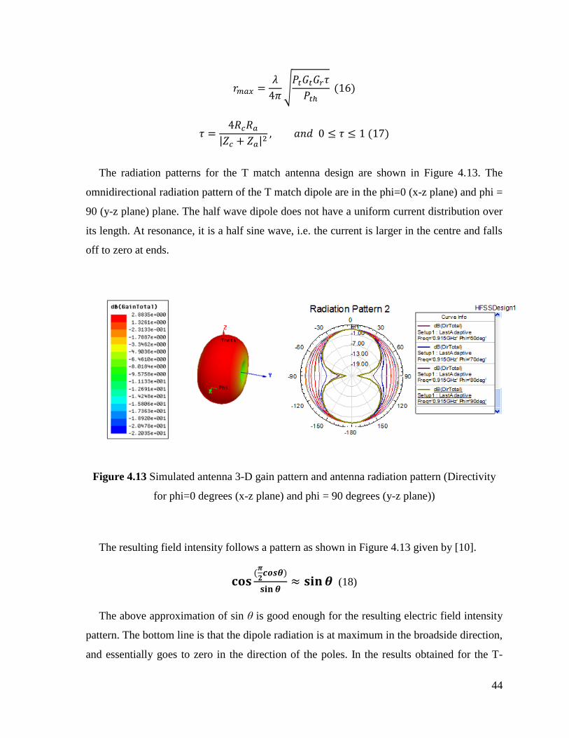
44
√
( )
| | ( )
The radiation patterns for the T match antenna design are shown in Figure 4.13. The
omnidirectional radiation pattern of the T match dipole are in the phi=0 (x-z plane) and phi =
90 (y-z plane) plane. The half wave dipole does not have a uniform current distribution over
its length. At resonance, it is a half sine wave, i.e. the current is larger in the centre and falls
off to zero at ends.
Figure 4.13 Simulated antenna 3-D gain pattern and antenna radiation pattern (Directivity
for phi=0 degrees (x-z plane) and phi = 90 degrees (y-z plane))
The resulting field intensity follows a pattern as shown in Figure 4.13 given by [10].
(
)
(18)
The above approximation of sin θ is good enough for the resulting electric field intensity
pattern. The bottom line is that the dipole radiation is at maximum in the broadside direction,
and essentially goes to zero in the direction of the poles. In the results obtained for the T-

45
match, since the antenna is placed horizontally, the radiation intensity is maximum at the
broadside direction ((phi=0 degrees (x-z plane) and phi = 90 degrees (y-z plane)) and nulls
(zero current intensity) at the ends (x-y plane). This makes the RFID tag antenna linearly
polarized- horizontal (LHP). Therefore, the reader antenna should either be of the same type
of LP (horizontal or vertical) or be circularly polarized (CP) in order to avoid polarization
mismatch and provide sufficient power to the tag antenna for communication.
Table 4.1 Simulated Antenna Parameters
Impedance
(Ohm)
Return Loss
(dB)
Gain
(dB)
Directivity
(dBi)
Antenna
Radiation
Efficiency
(%)
Theoretical
Read Range
(m)
14.18 + j141.18 41.12 2.372 2.884 82.2 2.914
The antenna radiation efficiency is given by the formula [19]. Here, G is the
gain of the antenna and D is the directivity and erad is the radiation efficiency. The read range
is given by the Friis free-space formula given by [5], equations (16), (17).
The chip to be used is Alien Higgs-2 ( ). The reader used is Alien ALR
9650 ( ), the antenna gain as given above and λ 0.33 m.
Using the equations (16) and (17) from [19], the antenna performance parameters such as
Gain, read range were calculated and shown in Table 4.4.
√
( )
| | ( )

46
4.5 HFSS Inductively Coupled Loop Simulation
4.5.1 Inductively Coupled Loop Antenna Design
The antenna is made of copper metal with thickness, 0.02 mm. The substrate is made of
polyester with thickness 0.1 mm (with εr = 3.2 and loss tangent δ = 0.003). Its dimensions
are width = 31.5 mm and length = 180 mm.
Figure 4.14 Inductively coupled loop RFID antenna design layout.
Figure 4.15 Inductively coupled loop configuration for planar dipoles [7].

47
The geometrical parameters of the antenna as shown in Figure 4.5.1 are as follows:
l = 163 mm
a = 20.1 mm
b = 20.1 mm
d = 3.9 mm
w = 3mm
w’ = 1 mm
Port separation = 2 mm
The IC impedance used for this design at 915 MHz has impedance 16 – j350 Ω (Phillips
EPC 1.19). That means the load antenna impedance should be 16 + j350 Ω for maximum
power transfer (conjugate matching). A different IC was used for the inductively coupled
loop design in order to demonstrate the antenna design process can be matched to different
ICs instead of just one unique IC.
4.5.2 Inductively Coupled Loop Simulation Results
The results below show the HFSS simulations results for the return loss and the
impedance.
Figure 4.16 Simulation results showing the return loss of the antenna.
0.60 0.70 0.80 0.90 1.00 1.10 1.20Freq [GHz]
-70.00
-60.00
-50.00
-40.00
-30.00
-20.00
-10.00
Re
turn
Lo
ss (
dB
)
Ansoft LLC HFSSDesign1Frequency vs Return Loss
m1
Curve Info
dB(S(1,1))Setup1 : Sw eep1
Name X Y
m1 0.8727 -62.1062
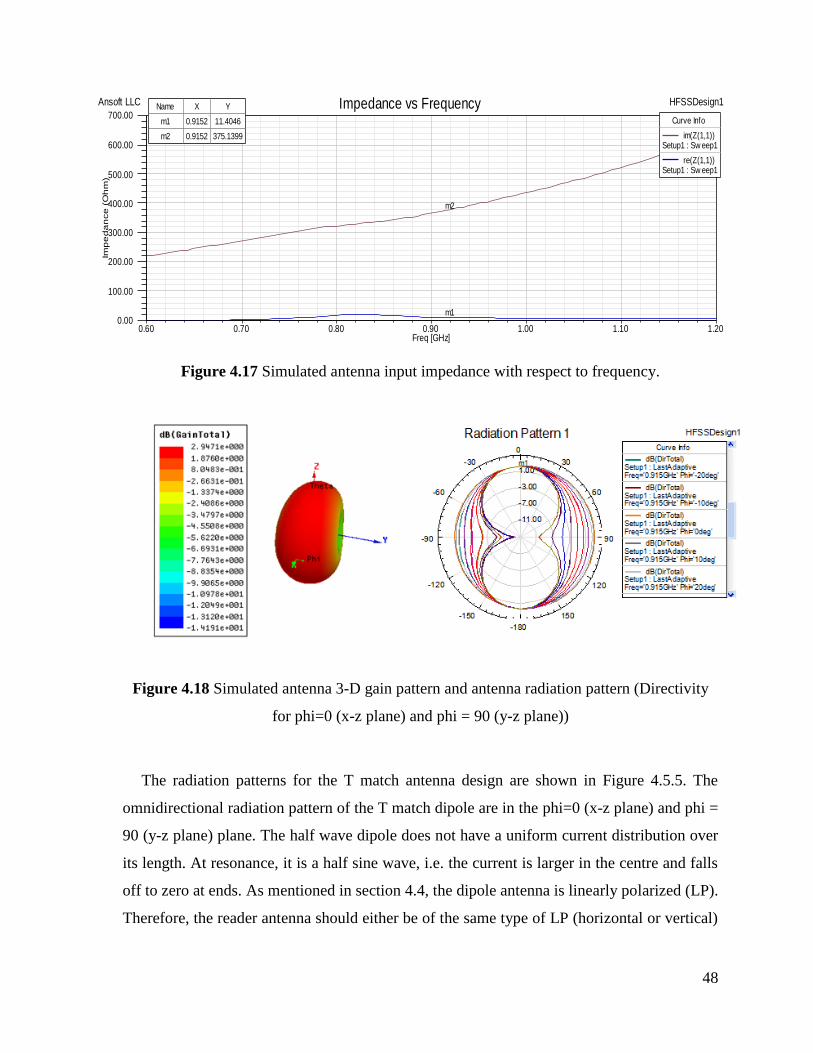
48
Figure 4.17 Simulated antenna input impedance with respect to frequency.
Figure 4.18 Simulated antenna 3-D gain pattern and antenna radiation pattern (Directivity
for phi=0 (x-z plane) and phi = 90 (y-z plane))
The radiation patterns for the T match antenna design are shown in Figure 4.5.5. The
omnidirectional radiation pattern of the T match dipole are in the phi=0 (x-z plane) and phi =
90 (y-z plane) plane. The half wave dipole does not have a uniform current distribution over
its length. At resonance, it is a half sine wave, i.e. the current is larger in the centre and falls
off to zero at ends. As mentioned in section 4.4, the dipole antenna is linearly polarized (LP).
Therefore, the reader antenna should either be of the same type of LP (horizontal or vertical)
0.60 0.70 0.80 0.90 1.00 1.10 1.20Freq [GHz]
0.00
100.00
200.00
300.00
400.00
500.00
600.00
700.00Im
pe
da
nce
(O
hm
)Ansoft LLC HFSSDesign1Impedance vs Frequency
m1
m2
Curve Info
im(Z(1,1))Setup1 : Sw eep1
re(Z(1,1))Setup1 : Sw eep1
Name X Y
m1 0.9152 11.4046
m2 0.9152 375.1399

49
or be circularly polarized (CP) in order to transfer sufficient power to the tag antenna for
communication.
Table 4.2 Simulated Antenna Parameters
Impedance
(Ohm)
Return Loss
(dB)
Gain
(dB)
Directivity
(dBi)
Antenna
Radiation
Efficiency
(%)
Theoretical
Read Range
(m)
11.40 + j375.14 62.10 2.350 2.947 79.7 1.56
The antenna radiation efficiency is given by the formula [19]. Here, G is the
gain of the antenna and D is the directivity. The read range is given by the Friis free-space
formula given above by [5]. The chip to be used is Phillips EPC 1.19 ( ). The
reader used is Alien ALR 9650 ( ) the antenna gain as given above
and λ 0.33 m.
4.6 HFSS Nested Slot Simulation
4.6.1 Nested Slot Antenna Design
The antenna is made of copper metal with thickness, 0.02 mm. The substrate is made of
polyester with thickness, 0.1 mm (with εr = 3.2 and loss tangent δ = 0.003) and its
dimensions are width = 31.5 mm and length = 180 mm.
The geometrical parameters of the antenna as shown in Figure 4.6.1 are as follows:
l = 163 mm
a = 45 mm
b = 23 mm
d = 2 mm
g = 2 mm
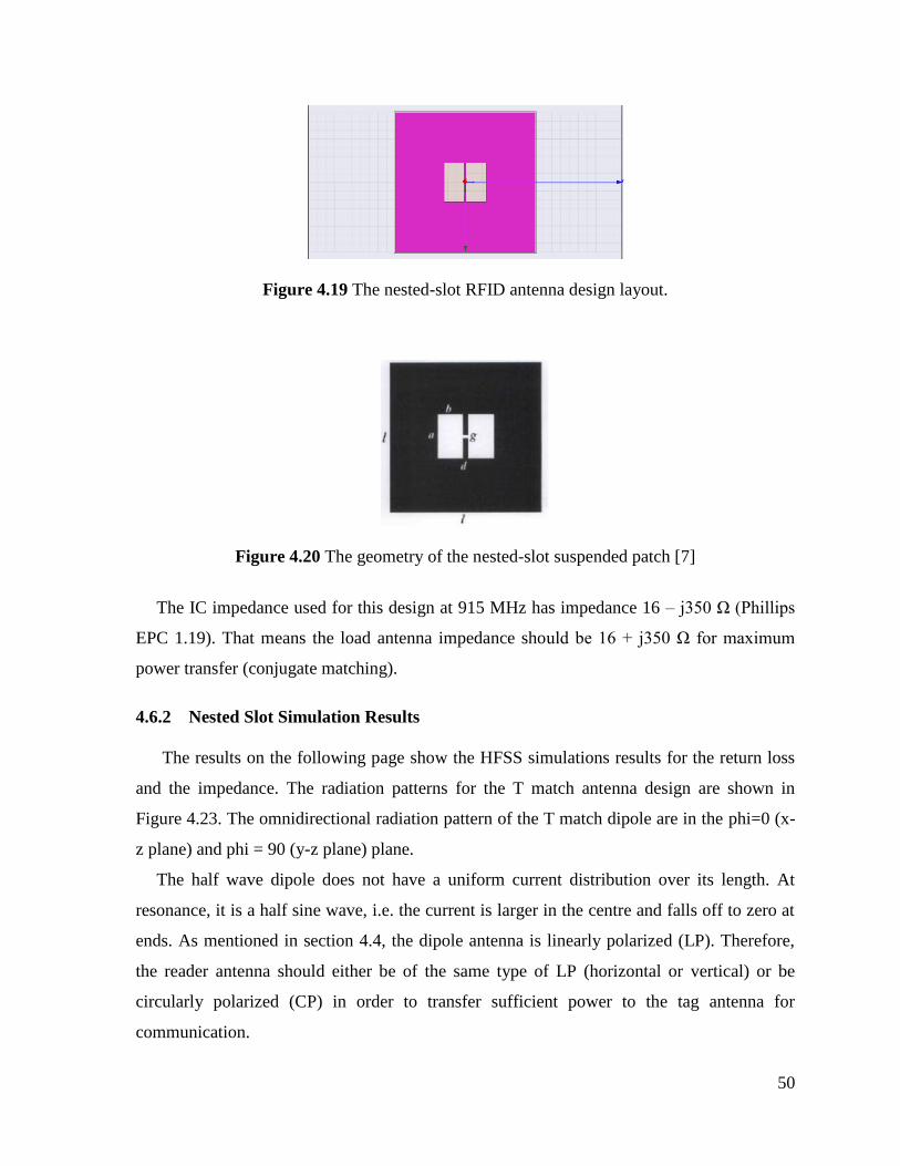
50
Figure 4.19 The nested-slot RFID antenna design layout.
Figure 4.20 The geometry of the nested-slot suspended patch [7]
The IC impedance used for this design at 915 MHz has impedance 16 – j350 Ω (Phillips
EPC 1.19). That means the load antenna impedance should be 16 + j350 Ω for maximum
power transfer (conjugate matching).
4.6.2 Nested Slot Simulation Results
The results on the following page show the HFSS simulations results for the return loss
and the impedance. The radiation patterns for the T match antenna design are shown in
Figure 4.23. The omnidirectional radiation pattern of the T match dipole are in the phi=0 (x-
z plane) and phi = 90 (y-z plane) plane.
The half wave dipole does not have a uniform current distribution over its length. At
resonance, it is a half sine wave, i.e. the current is larger in the centre and falls off to zero at
ends. As mentioned in section 4.4, the dipole antenna is linearly polarized (LP). Therefore,
the reader antenna should either be of the same type of LP (horizontal or vertical) or be
circularly polarized (CP) in order to transfer sufficient power to the tag antenna for
communication.
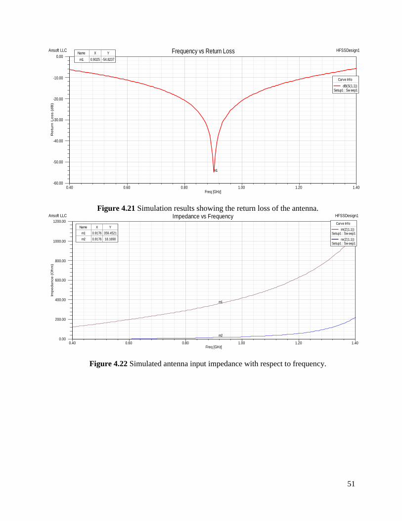
51
Figure 4.21 Simulation results showing the return loss of the antenna.
Figure 4.22 Simulated antenna input impedance with respect to frequency.
0.40 0.60 0.80 1.00 1.20 1.40Freq [GHz]
-60.00
-50.00
-40.00
-30.00
-20.00
-10.00
0.00R
etu
rn L
oss (
dB
)Ansoft LLC HFSSDesign1Frequency vs Return Loss
m1
Curve Info
dB(S(1,1))Setup1 : Sw eep1
Name X Y
m1 0.9025 -54.8237
0.40 0.60 0.80 1.00 1.20 1.40Freq [GHz]
0.00
200.00
400.00
600.00
800.00
1000.00
1200.00
Imp
ed
an
ce
(O
hm
)
Ansoft LLC HFSSDesign1Impedance vs Frequency
m1
m2
Curve Info
im(Z(1,1))Setup1 : Sw eep1
re(Z(1,1))Setup1 : Sw eep1
Name X Y
m1 0.9176 359.4521
m2 0.9176 18.1690

52
Figure 4.23 Simulated antenna 3-D gain pattern and antenna radiation pattern (Directivity
for phi=0 (x-z plane) and phi = 90 (y-z plane))
The antenna radiation efficiency is given by the formula [19]. Here, G is the
gain of the antenna and D is the directivity. The read range is given by the Friis free-space
formula given by [13]. The chip to be used is Phillips EPC 1.19 ( ). The
reader used is Alien ALR 9650 ( ), the antenna gain as given above
and λ 0.33 m.
Table 4.3 Simulated Antenna Parameters
Impedance
(Ohm)
Return Loss
(dB)
Gain
(dB)
Directivity
(dBi)
Antenna
Radiation
Efficiency (%)
Theoretical
Read Range
(m)
18.17 + j359.45 54.82 3.928 4.116 95.4 2.49
Table 4.6.2 The simulated return loss and impedance value comparison for the above cases
shown below
Return Loss Simulated Impedance
Value
Desired Impedance
Value
T-Match 41.118 dB 14.2 + j141.18 Ω 12 + j140 Ω
Inductively Coupled Loop 62.108 dB 11.4 + j375.14 Ω 16 + j350 Ω
Nested Slot 54.803 dB 18.2 + j359.40 Ω 16 + j350 Ω

53
4.7 Summary
In this chapter we discussed different methodologies for the design of UHF RFID (915
MHz) passive tag elements. These design methodologies include T-match, inductively
coupled loop, and nested-slot. All three designs are conjugate matching techniques used to
conjugate match the input impedance of the IC. The geometry of the antenna design
determines the impedance value of the antennas which generally have low resistance and
high inductance. In this chapter, all three designs were simulated using Ansoft HFSS antenna
design tool. The simulation results were in close agreement to the desired antenna
impedance as seen in Figure 4.6.2. Further optimization of the antenna geometry may
improve the conjugate matching. Consequently, the RFID tag antenna will resonate at the
required frequency (915 MHz) and improve the most important tag performance requirement
‘read range’.

54
CHAPTER 5 – Classification of commercially available RFID tags
Passive UHF RFID antennas are mainly based on a “printed” dipole configuration [10].
Figure 5.1 shows several commercial tags. As seen in Figure 5.1, the tags have interesting
geometries such as long and skinny dipoles, slots, curves and wiggles. The RFID-IC is
attached to a loop within the antenna structure. Most of the features are designed for a
functional purpose, i.e. they affect the behavior of the antenna to meet a specific design goal.
In this chapter, a literary survey is examined to classify existing passive RFID tags into a
family or class based on their application of use. The chapter is divided into three parts; the
first part introduces the dipole geometry and radiation resistance. The second part highlights
the size reduction techniques such as meandering dipoles and inverted-F configurations. The
last section deals with classification of RFID tags into a family based on their application.
5.1 Dipoles
The classic dipole antenna Figure 5.2 consists of two cylindrical wires of equal length
placed in a line with an ac source in the middle.
Figure 5.1 Variety of commercially available tags [10].
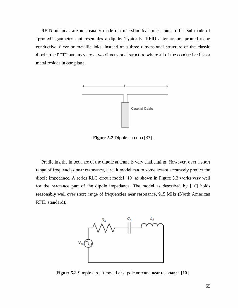
55
RFID antennas are not usually made out of cylindrical tubes, but are instead made of
“printed” geometry that resembles a dipole. Typically, RFID antennas are printed using
conductive silver or metallic inks. Instead of a three dimensional structure of the classic
dipole, the RFID antennas are a two dimensional structure where all of the conductive ink or
metal resides in one plane.
Figure 5.2 Dipole antenna [33].
Predicting the impedance of the dipole antenna is very challenging. However, over a short
range of frequencies near resonance, circuit model can to some extent accurately predict the
dipole impedance. A series RLC circuit model [10] as shown in Figure 5.3 works very well
for the reactance part of the dipole impedance. The model as described by [10] holds
reasonably well over short range of frequencies near resonance, 915 MHz (North American
RFID standard).
Figure 5.3 Simple circuit model of dipole antenna near resonance [10].
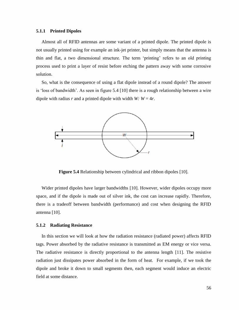
56
5.1.1 Printed Dipoles
Almost all of RFID antennas are some variant of a printed dipole. The printed dipole is
not usually printed using for example an ink-jet printer, but simply means that the antenna is
thin and flat, a two dimensional structure. The term ‘printing’ refers to an old printing
process used to print a layer of resist before etching the pattern away with some corrosive
solution.
So, what is the consequence of using a flat dipole instead of a round dipole? The answer
is ‘loss of bandwidth’. As seen in figure 5.4 [10] there is a rough relationship between a wire
dipole with radius r and a printed dipole with width W: W = 4r.
Figure 5.4 Relationship between cylindrical and ribbon dipoles [10].
Wider printed dipoles have larger bandwidths [10]. However, wider dipoles occupy more
space, and if the dipole is made out of silver ink, the cost can increase rapidly. Therefore,
there is a tradeoff between bandwidth (performance) and cost when designing the RFID
antenna [10].
5.1.2 Radiating Resistance
In this section we will look at how the radiation resistance (radiated power) affects RFID
tags. Power absorbed by the radiative resistance is transmitted as EM energy or vice versa.
The radiative resistance is directly proportional to the antenna length [11]. The resistive
radiation just dissipates power absorbed in the form of heat. For example, if we took the
dipole and broke it down to small segments then, each segment would induce an electric
field at some distance.
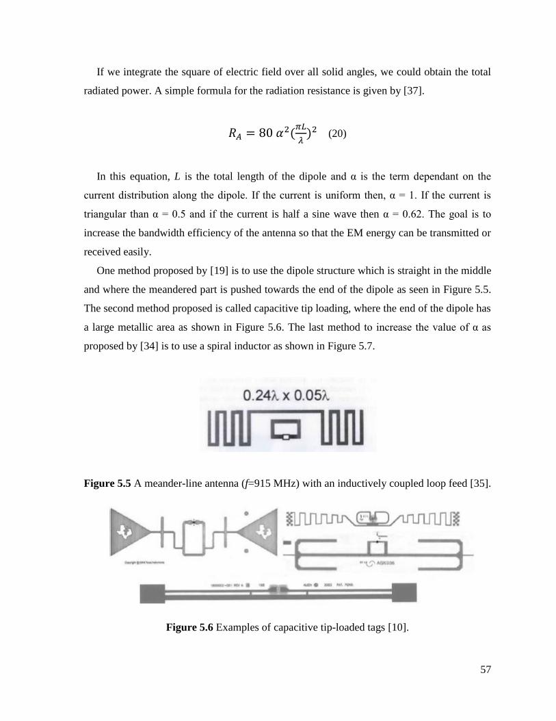
57
If we integrate the square of electric field over all solid angles, we could obtain the total
radiated power. A simple formula for the radiation resistance is given by [37].
(
) (20)
In this equation, L is the total length of the dipole and α is the term dependant on the
current distribution along the dipole. If the current is uniform then, α = 1. If the current is
triangular than α = 0.5 and if the current is half a sine wave then α = 0.62. The goal is to
increase the bandwidth efficiency of the antenna so that the EM energy can be transmitted or
received easily.
One method proposed by [19] is to use the dipole structure which is straight in the middle
and where the meandered part is pushed towards the end of the dipole as seen in Figure 5.5.
The second method proposed is called capacitive tip loading, where the end of the dipole has
a large metallic area as shown in Figure 5.6. The last method to increase the value of α as
proposed by [34] is to use a spiral inductor as shown in Figure 5.7.
Figure 5.5 A meander-line antenna (f=915 MHz) with an inductively coupled loop feed [35].
Figure 5.6 Examples of capacitive tip-loaded tags [10].

58
Figure 5.7 Example of spiral-loaded tag. [10].
5.2 Size Reduction Techniques
Most UHF RFID tags have to be attached to small objects. The dipole as described in
section 5.1.1 has to be reduced in length to fit the tag’s area as well as not degrade in
radiation efficiency. Two methods to achieve this are meandering and inverted-F
configurations. Both configurations require a single or multiple folding of the radiating body
in order to accommodate the length required for achieving resonance at a particular
frequency. Matching charts may be used in the design of simple layouts or optimization tools
can be used where a large geometry (many parameters) is used.
5.2.1 Meandering Diploes
The dipole antenna arms are folded along a meandered path as proposed by [7] and shown
in Figure 5.8. The wire configuration produced has distributed capacitive and inductive
reactance that effect the overall antenna’s input impedance. The transmission-line currents
do not give a valuable contribution to the radiated power, but instead produce losses.
Resonances are achieved at lower frequencies when compared to straight dipoles. In
addition, the bandwidth is reduced along with low efficiency.
The shape of the meandered dipole can be periodic or individually optimized to match the
chip impedance. As seen in the figures 5.8 to 5.14, the total length of the meander-line
antenna increases along with the reactance, and the height of the meandered segment
controls the resistance.

59
Figure 5.8 The geometry of the meander line antenna with multiple unequal turns. The
horizontal lines control the radiation resistance, the adjacent vertical lines act as energy
storage elements, and the overall conductor length affects the inductance [7]
Figure 5.9 An equi-spaced meander line antenna (f=953 MHz) with the T-match feed [36]
Figure 5.10 A meander-line antenna (f=915 MHz) with an inductively coupled loop feed
[37].

60
Figure 5.11 A meander-line antenna (f=920 MHz) with a loading bar. The antenna’s
reactance and resistance can be controlled by trimming the meander-line antenna and the bar
by punching holes [37].
Figure 5.12 A multi-conductor antenna (f=900 MHz) with a double T-match scheme and
spiral folding, used to achieve the required inductance. The extra material at the end as
discussed in section 1.5 helps increase the antenna’s bandwidth [38]
Figure 5.13 A text-shaped meander-line antenna (f=870 MHz) where the turns are obtained
by attaching the adjacent letters of the text [39]
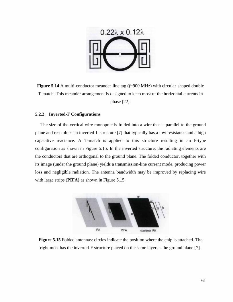
61
Figure 5.14 A multi-conductor meander-line tag (f=900 MHz) with circular-shaped double
T-match. This meander arrangement is designed to keep most of the horizontal currents in
phase [22].
5.2.2 Inverted-F Configurations
The size of the vertical wire monopole is folded into a wire that is parallel to the ground
plane and resembles an inverted-L structure [7] that typically has a low resistance and a high
capacitive reactance. A T-match is applied to this structure resulting in an F-type
configuration as shown in Figure 5.15. In the inverted structure, the radiating elements are
the conductors that are orthogonal to the ground plane. The folded conductor, together with
its image (under the ground plane) yields a transmission-line current mode, producing power
loss and negligible radiation. The antenna bandwidth may be improved by replacing wire
with large strips (PIFA) as shown in Figure 5.15.
Figure 5.15 Folded antennas: circles indicate the position where the chip is attached. The
right most has the inverted-F structure placed on the same layer as the ground plane [7].
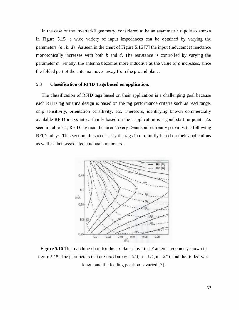
62
In the case of the inverted-F geometry, considered to be an asymmetric dipole as shown
in Figure 5.15, a wide variety of input impedances can be obtained by varying the
parameters a , b, d. As seen in the chart of Figure 5.16 [7] the input (inductance) reactance
monotonically increases with both b and d. The resistance is controlled by varying the
parameter d. Finally, the antenna becomes more inductive as the value of a increases, since
the folded part of the antenna moves away from the ground plane.
5.3 Classification of RFID Tags based on application.
The classification of RFID tags based on their application is a challenging goal because
each RFID tag antenna design is based on the tag performance criteria such as read range,
chip sensitivity, orientation sensitivity, etc. Therefore, identifying known commercially
available RFID inlays into a family based on their application is a good starting point. As
seen in table 5.1, RFID tag manufacturer ‘Avery Dennison’ currently provides the following
RFID Inlays. This section aims to classify the tags into a family based on their applications
as well as their associated antenna parameters.
Figure 5.16 The matching chart for the co-planar inverted-F antenna geometry shown in
figure 5.15. The parameters that are fixed are w = λ/4, u = λ/2, a = λ/10 and the folded-wire
length and the feeding position is varied [7].

63
Figure 5.17 A conventional two-layer PIFA (f=870 MHz) with a square conductor [7].
Figure 5.18 A two-layer double PIFA tag with proximity feed loop (f=900 MHz). The
microchip is placed on the top metallization [40].
Figure 5.19 A co-planar IFA (f=870 MHz) with an additional horizontal stub [41].

64
Table 5.1a Antennas marketed by Avery Dennison [42].
Tag
#
Antenna Type Dimension
s (mm) Applications
Antenna Parameters
linked to literature
papers.
1.
95 x 8.15
General purpose
applications, with
medium read
range.
Modified T-Match, no
meandering. Therefore,
low resonance frequency
[42], [43].
2.
70 x 14.5 Distance reading
Modified T-Match, with
meandering. Therefore,
good resonance
frequency [42], [44].
3.
70 x 14.5
Stock
management. Low
read range
Modified T-Match, with
meandering and
capacitive tip-loading at
ends (section 5.1.2)
Therefore, good
resonance frequency,
good radiation resistance,
increased cost –more
metal used [42], [45].
4.
50 x 30
Ideal for media
denim and cotton
based on
mechanical
properties of
antenna.
Modified T-Match, with
less meandering and
capacitive tip-loading at
ends (section 5.1.2)
Therefore, lower
resonance frequency,
good radiator, increased
cost – [42], [46].

65
Table 5.1b Antennas marketed by Avery Dennison [42].
5.
70 x 70
Uniform radiation
pattern. Ideal for
card support.
PIFA configuration.
Large metallic surface.
Good resonance
frequency, high radiation
resistance, increased cost
[42], [47].
6.
16 x 16
Very compact.
Used on metal
supports.
IC pushed to one corner.
Small meander. Small
size. Good resonating
frequency, high radiation
resistance. Increased cost
(metal surface – refer to
section 5.3) [42], [48].
7.
22 x 22
For
pharmaceutical
products of
various sizes and
shapes.
PIFA configuration.
Large metallic surface.
Good resonating
frequency, high radiation
resistance, increased cost
[42], [49].
8.
20 x 10
Excellent on glass
support. Used in
the United States
and Japan.
One-sided meandering,
monopole structure, good
resonance frequency,
reasonable cost [42],
[46].
9.
29.99 x 50 For retail sale of
various products.
Spiral loaded tag.
Excellent radiation
resistance [42].

66
Table 5.1c Antennas marketed by Avery Dennison [42].
10.
18 x 40
Long read range
distance. Mainly
used in the
medical field
because of small
size and
mitigation of the
effects of liquids.
Modified T-Match, with
higher meandering and
capacitive tip-loading at
ends (section 5.1.2)
Therefore, good
resonance frequency,
increased cost [42], [50].
11.
Unknown.
Expected to
be larger
than most
tags in size.
Orientation
Insensitive.
Dual-Dipole RFID tag.
Able to deal with
polarization mismatch.
Lower Q, good
resonance. However
increased cost (2 RF
feeds on IC, plus the
metal area) [42], [10].
As seen in table 5.1, the RFID inlays are manufactured based on their applications of use
such as retail, clothing, healthcare, pharmaceutical, distance reading, metal supports, etc.
Furthermore, the antenna parameters associated with the RFID inlays such as T-match,
meandering, capacitive tip-loading, high radiation resistance, etc are also mentioned in the
table. Note, good resonance frequency in table 5.1 indicates that the desired antenna return
loss value (>10 dB) is close to the frequency of operation, 915MHz.
Now each of these designs is classified into a family based on their application of use
shown in table 5.2. The tags are classified into a family based on their applications. The tag
numbers ‘A, B, C, D and E’ in table 5.2 represent the tag designs for each application and
will be presented in the next chapter.

67
Table 5.2 Family of RFID tags based on application
Application Tag Number
1) Broad Band tag (universal RFID bandwidth) 2,4,11, A
2) General purpose tag (Clothing, books) 1, 9, B
3) Medical, healthcare 6,7,8,10,11,C
4) Baggage tag 3, D
5) Contactless card 5, E
5.4 Chapter Summary
In this chapter, a literary survey is examined to classify existing passive RFID tags into a
family or class based on their application or use. The first section introduced to dipole
geometry and radiation resistance necessary to understand how tags are manufactured in
industry. Second, size reduction techniques such as meandering dipoles and inverted-F
configurations were studied with respect to changes in the geometrical parameters of the
design. Finally, the classification of RFID tags into a family based on their application as
presented in table 5.2, was discussed and a few designs (A, B, C, D and E) that will be
simulated and fabricated will be presented in the following chapters.

68
CHAPTER 6 – Simulation of antennas design using HFSS
Passive RFID tags are usually analyzed using electromagnetic modeling and simulation
tools such as method of moments (MoM) for planar designs and finite element method
(FEM) or finite-difference time-domain (FDTD) methods for other designs. Fast EM
analysis tools such as Ansoft HFSS are very important for efficient tag design. For example,
the geometrical parameters (height, width) of a meandered dipole antenna designed using
HFSS can be investigated to see how incremental changes effect tag performance
(impedance, frequency, etc).
In this chapter the simulation results of the designed tags based on the application of use
as shown in table 6.1 are presented. The chapter is divided into three parts; the first part
briefly introduces the different antenna designs ‘A, B, C, D and E’ and the advantages for
using the particular shape. The second part examines the parametric study and optimization
of the proposed antenna geometry using the FEM design tool. Finally, the simulations results
are investigated to find the best possible geometrical dimensions for the proposed antennas.
Table 6.1 Family of RFID tags based on application
Application Tag Number
1. Broad Band tag (universal RFID bandwidth) A
2. General purpose tag (Clothing, books) B
3. Medical, healthcare C
4. Baggage tag D
5. Contactless card E
6.1 Proposed Antenna Designs
In this section the proposed antenna designs based on the application as seen in table 6.1
are presented. The antenna designs are chosen specifically based on size reduction and
impedance matching techniques [7], [5] such as T-match, meandering, capacitive tip-
loading, etc. The goal is to design antennas that will provide optimal tag performance
characteristics for the given application.
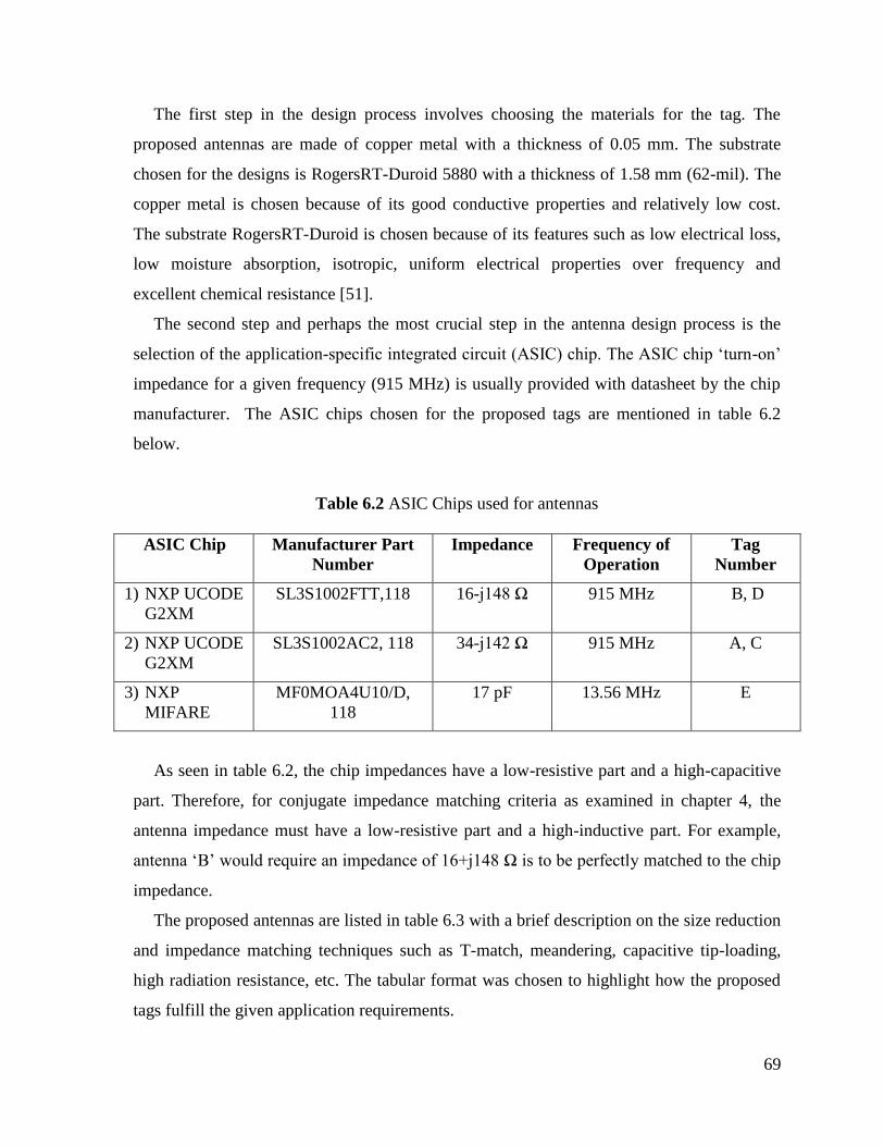
69
The first step in the design process involves choosing the materials for the tag. The
proposed antennas are made of copper metal with a thickness of 0.05 mm. The substrate
chosen for the designs is RogersRT-Duroid 5880 with a thickness of 1.58 mm (62-mil). The
copper metal is chosen because of its good conductive properties and relatively low cost.
The substrate RogersRT-Duroid is chosen because of its features such as low electrical loss,
low moisture absorption, isotropic, uniform electrical properties over frequency and
excellent chemical resistance [51].
The second step and perhaps the most crucial step in the antenna design process is the
selection of the application-specific integrated circuit (ASIC) chip. The ASIC chip ‘turn-on’
impedance for a given frequency (915 MHz) is usually provided with datasheet by the chip
manufacturer. The ASIC chips chosen for the proposed tags are mentioned in table 6.2
below.
Table 6.2 ASIC Chips used for antennas
ASIC Chip Manufacturer Part
Number
Impedance Frequency of
Operation
Tag
Number
1) NXP UCODE
G2XM
SL3S1002FTT,118 16-j148 Ω 915 MHz B, D
2) NXP UCODE
G2XM
SL3S1002AC2, 118 34-j142 Ω 915 MHz A, C
3) NXP
MIFARE
MF0MOA4U10/D,
118
17 pF 13.56 MHz E
As seen in table 6.2, the chip impedances have a low-resistive part and a high-capacitive
part. Therefore, for conjugate impedance matching criteria as examined in chapter 4, the
antenna impedance must have a low-resistive part and a high-inductive part. For example,
antenna ‘B’ would require an impedance of 16+j148 Ω is to be perfectly matched to the chip
impedance.
The proposed antennas are listed in table 6.3 with a brief description on the size reduction
and impedance matching techniques such as T-match, meandering, capacitive tip-loading,
high radiation resistance, etc. The tabular format was chosen to highlight how the proposed
tags fulfill the given application requirements.

70
Table 6.3a Proposed Antenna Design based on specific applications.
Tag # Antenna Type Dimension
s (mm) Applications
Antenna size reduction
and Impedance
Matching techniques
A.
97.5 x 34.7
Broadband tag
(universal RFID
bandwidth, 868-
960 MHz)
Inductively coupled
loop, minimal
meandering, capacitive
tip-loaded. Therefore,
increased bandwidth.
B.
94 x 18.5
General purpose
tag (Clothing,
books)
Inductively coupled-
loop Match, with
meandering.
Therefore, good
resonance frequency.
C.
120 x 40 Medical,
healthcare
Two-wire folded
dipole, and capacitive
tip-loading. Therefore,
increased read range,
good radiation
resistance, increased
cost –more metal used.

71
The exact dimensions of the proposed antennas are individually shown in Figure 6.1. The
dimensions of the antenna were chosen. The FEM simulation tool is used for modeling the
antennas A-D parameters such as return loss, load impedance, read range, etc. However, for
design ‘E’ the antenna design software provided by [52] is used to model the exact
dimensions necessary for conjugate impedance matching with the chip impedance (17 pF).
Table 6.3b Proposed Antenna Design based on specific applications.
D.
94 x 24.5 Baggage tag
Inductively coupled-
loop Match, with less
meandering and
capacitive tip-loading
at ends. Therefore,
lower resonance
frequency, good
radiator and increased
cost.
E.
100 x 60 Contactless card
Square coil structure
[4]. Good resonance
frequency, high
radiation resistance,
increased cost because
more size and material
used.
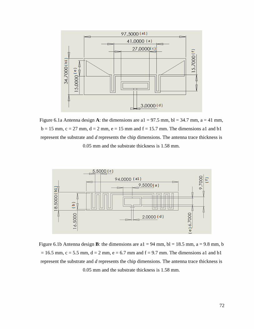
72
Figure 6.1a Antenna design A: the dimensions are a1 = 97.5 mm, bl = 34.7 mm, a = 41 mm,
b = 15 mm, c = 27 mm, d = 2 mm, e = 15 mm and f = 15.7 mm. The dimensions a1 and b1
represent the substrate and d represents the chip dimensions. The antenna trace thickness is
0.05 mm and the substrate thickness is 1.58 mm.
Figure 6.1b Antenna design B: the dimensions are a1 = 94 mm, bl = 18.5 mm, a = 9.8 mm, b
= 16.5 mm, c = 5.5 mm, d = 2 mm, e = 6.7 mm and f = 9.7 mm. The dimensions a1 and b1
represent the substrate and d represents the chip dimensions. The antenna trace thickness is
0.05 mm and the substrate thickness is 1.58 mm.

73
Figure 6.1c Antenna design C: the dimensions are a1 = 120 mm, bl = 40 mm, a = 50 mm, b
= 23 mm, c = 32 mm, d = 4 mm and e = 19 mm. The dimensions a1 and b1 represent the
substrate and d represents the chip dimensions. The antenna trace thickness is 0.05 mm and
the substrate thickness is 1.58 mm.
Figure 6.1d Antenna design D: the dimensions are a1 = 94 mm, bl = 24.5 mm, a = 44 mm, b
= 20.5 mm, c = 19 mm, d = 2 mm, e = 7.5 mm, f = 5.5mm, g = 15 mm, h = 9.7mm and i =
6.7mm. The dimensions a1 and b1 represent the substrate and d represents the chip
dimensions. The antenna trace thickness is 0.05 mm and the substrate thickness is 1.58 mm.

74
Figure 6.1e Antenna design E: the dimensions are a1 = 100 mm, bl = 60 mm, a = 80 mm, b
= 40 mm. The dimensions a1 and b1 represent the substrate dimensions. The antenna trace
thickness is 0.05 mm and the substrate thickness is 1.58 mm.
Figure 6.1 Dimensions of the proposed antenna designs.
6.2 Optimization of antenna design using HFSS simulations
This section highlights the antenna parameters such as return loss, load impedance, read
range, etc. using HFSS simulations. Furthermore, the optimization of the antenna design is
achieved by varying the geometrical parameters and analyzing the impact on tag
performance (impedance, return loss, etc). For the simulation setup in this chapter the
antenna impedance is matched to the impedance of the IC.
6.2.1 Simulation results without optimization
The return loss with respect to frequency for antenna designs A-D is shown in figure 6.2
below.

75
Figure 6.2a Simulation results showing the return loss of the antenna A
As seen from Figure 6.2a the antenna has a bandwidth > 70 MHz at a return loss (RL) >
10dB which covers the worldwide RFID UHF band.
Figure 6.2b Simulation results showing the return loss of the antenna B
As seen from Figure 6.2b the antenna has a bandwidth > 70 MHz at a return loss (RL) >
10dB.
0.50 0.60 0.70 0.80 0.90 1.00 1.10 1.20Freq [GHz]
-27.50
-22.50
-17.50
-12.50d
B(S
(1
,1))
Ansoft LLC HFSSDesign1Frequency vs Return Loss
m2
m1
Curve Info
dB(S(1,1))Setup1 : Sw eep1
Name X Y
m1 0.8670 -21.4471
m2 0.9150 -19.9142
0.50 0.60 0.70 0.80 0.90 1.00 1.10 1.20Freq [GHz]
-50.00
-45.00
-40.00
-35.00
-30.00
-25.00
-20.00
-15.00
-10.00
-5.00
dB
(S(1
,1))
Ansoft LLC HFSSDesign1Frequency vs Return Loss
m1
Curve Info
dB(S(1,1))Setup1 : Sw eep1
Name X Y
m1 0.9150 -41.1578
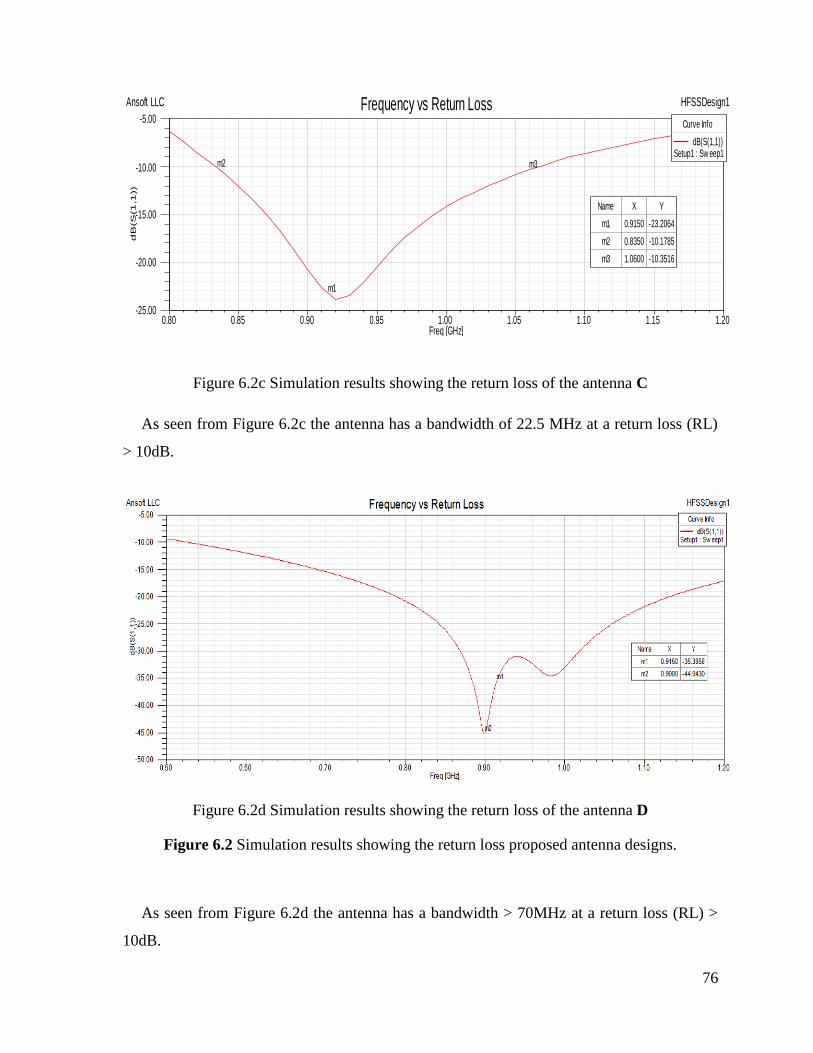
76
Figure 6.2c Simulation results showing the return loss of the antenna C
As seen from Figure 6.2c the antenna has a bandwidth of 22.5 MHz at a return loss (RL)
> 10dB.
Figure 6.2d Simulation results showing the return loss of the antenna D
Figure 6.2 Simulation results showing the return loss proposed antenna designs.
As seen from Figure 6.2d the antenna has a bandwidth > 70MHz at a return loss (RL) >
10dB.
0.80 0.85 0.90 0.95 1.00 1.05 1.10 1.15 1.20Freq [GHz]
-25.00
-20.00
-15.00
-10.00
-5.00d
B(S
(1
,1))
Ansoft LLC HFSSDesign1Frequency vs Return Loss
m1
m3m2
Curve Info
dB(S(1,1))Setup1 : Sw eep1
Name X Y
m1 0.9150 -23.2064
m2 0.8350 -10.1785
m3 1.0600 -10.3516

77
The results obtained in figure 6.2 show that the antenna have a minimum return loss (RL)
> 10dB which is standard while designing RFID tag antennas [5]. The next simulation
results of interest are the impedance versus frequency. At 915 MHz, the impedance of the
simulated results should conjugate match with the chip impedance as seen in figure 6.3.
As seen from Figure 6.3a the simulated resistance and reactance at the required frequency
(915MHz) is 10.99 + j180.9 respectively. This is very close to the required impedance of 16
+ j148 Ω required for conjugate matching.
Figure 6.3a Simulation results showing the impedance of the antenna A
Figure 6.3b Simulation results showing the impedance of the antenna B
0.50 0.60 0.70 0.80 0.90 1.00 1.10 1.20Freq [GHz]
0.00
50.00
100.00
150.00
200.00
250.00
300.00
Y1
Ansoft LLC HFSSDesign1Frequency vs Impedance
m1
m2
Curve Info
im(Z(1,1))Setup1 : Sw eep1
re(Z(1,1))Setup1 : Sw eep1
Name X Y
m1 0.9150 10.9919
m2 0.9150 180.9553
0.50 0.60 0.70 0.80 0.90 1.00 1.10 1.20Freq [GHz]
0.00
25.00
50.00
75.00
100.00
125.00
150.00
175.00
200.00
Y1
Ansoft LLC HFSSDesign1Frequency vs Impedance
m1
m2
Curve Info
im(Z(1,1))Setup1 : Sw eep1
re(Z(1,1))Setup1 : Sw eep1
Name X Y
m1 0.9150 18.0872
m2 0.9150 146.4592
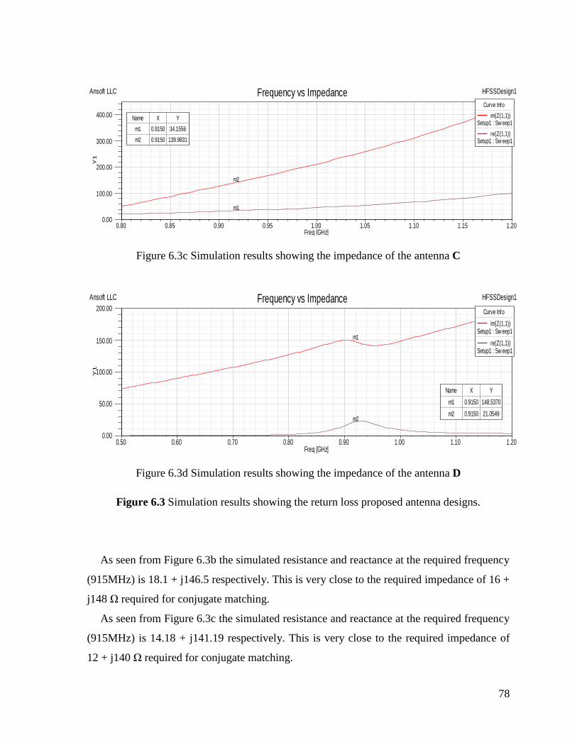
78
Figure 6.3c Simulation results showing the impedance of the antenna C
Figure 6.3d Simulation results showing the impedance of the antenna D
Figure 6.3 Simulation results showing the return loss proposed antenna designs.
As seen from Figure 6.3b the simulated resistance and reactance at the required frequency
(915MHz) is 18.1 + j146.5 respectively. This is very close to the required impedance of 16 +
j148 Ω required for conjugate matching.
As seen from Figure 6.3c the simulated resistance and reactance at the required frequency
(915MHz) is 14.18 + j141.19 respectively. This is very close to the required impedance of
12 + j140 Ω required for conjugate matching.
0.80 0.85 0.90 0.95 1.00 1.05 1.10 1.15 1.20Freq [GHz]
0.00
100.00
200.00
300.00
400.00
Y1
Ansoft LLC HFSSDesign1Frequency vs Impedance
m1
m2
Curve Info
im(Z(1,1))Setup1 : Sw eep1
re(Z(1,1))Setup1 : Sw eep1
Name X Y
m1 0.9150 34.1556
m2 0.9150 139.9831
0.50 0.60 0.70 0.80 0.90 1.00 1.10 1.20Freq [GHz]
0.00
50.00
100.00
150.00
200.00
Y1
Ansoft LLC HFSSDesign1Frequency vs Impedance
m1
m2
Curve Info
im(Z(1,1))Setup1 : Sw eep1
re(Z(1,1))Setup1 : Sw eep1
Name X Y
m1 0.9150 148.5370
m2 0.9150 21.0549
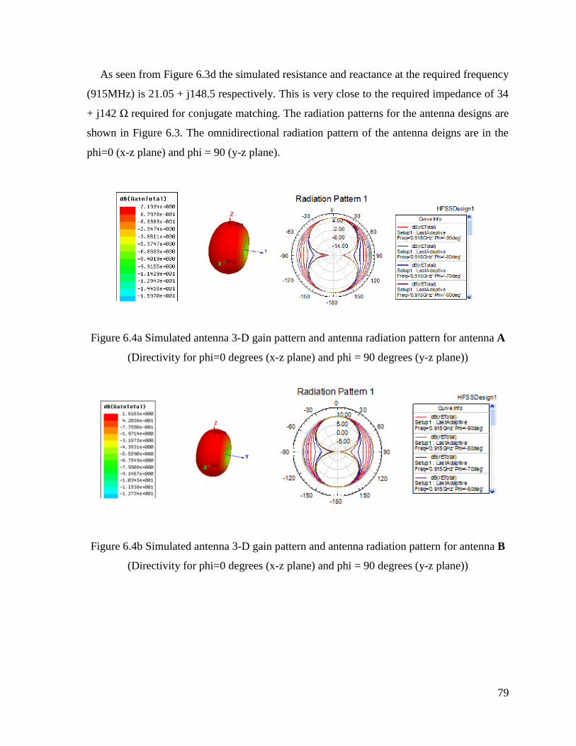
79
As seen from Figure 6.3d the simulated resistance and reactance at the required frequency
(915MHz) is 21.05 + j148.5 respectively. This is very close to the required impedance of 34
+ j142 Ω required for conjugate matching. The radiation patterns for the antenna designs are
shown in Figure 6.3. The omnidirectional radiation pattern of the antenna deigns are in the
phi=0 (x-z plane) and phi = 90 (y-z plane).
Figure 6.4a Simulated antenna 3-D gain pattern and antenna radiation pattern for antenna A
(Directivity for phi=0 degrees (x-z plane) and phi = 90 degrees (y-z plane))
Figure 6.4b Simulated antenna 3-D gain pattern and antenna radiation pattern for antenna B
(Directivity for phi=0 degrees (x-z plane) and phi = 90 degrees (y-z plane))

80
Figure 6.4c Simulated antenna 3-D gain pattern and antenna radiation pattern for antenna C
(Directivity for phi=0 degrees (x-z plane) and phi = 90 degrees (y-z plane))
Figure 6.4d Simulated antenna 3-D gain pattern and antenna radiation pattern for antenna D
(Directivity for phi=0 degrees (x-z plane) and phi = 90 degrees (y-z plane))
Figure 6.4 Simulation results showing the 3-D gain pattern and radiation pattern of the
proposed antenna designs.
The antenna radiation efficiency is given by the formula [19]. Here, G is the
gain of the antenna and D is the directivity. The read range is given by the Friis free-space
formula given by [5] equations (16), (17).

81
The chip to be used is NXP UCODE G2XM ( ). The reader used is
Convergence Systems Ltd CS203 ( ), the antenna gain as given
above and λ 0.33 m. The results are shown in table 6.4. The impedance matching
comparison for the antenna design is shown in table 6.5.
√
( )
| | ( )
Table 6.4 Simulated Antenna Parameters
Antenna Impedance
(Ohm)
Return
Loss (dB)
Gain
(dB)
Directivity
(dBi)
Antenna
Radiation
Efficiency
(%)
Theoretical
Read Range
(m)
Antenna
A
10.99 + j180.9 Ω 19.91 dB 2.193 2.929 74.8 9.86
Antenna
B
18.10 + j146.5 Ω 41.16 dB 1.616 2.544 63.5 11.76
Antenna
C
14.18 + j141.2 Ω 23.21 dB 2.326 2.327 99.9 8.21
Antenna
D
21.05 + j148.5 Ω 35.39 dB 1.905 2.564 74.3 12.68
Table 6.5 The simulated return loss and impedance value comparison for the antenna
designs.
Antenna Return Loss Simulated Impedance
Value
Desired Impedance
Value
Antenna A 19.91 dB 10.99 + j180.9 Ω 16 + j148 Ω
Antenna B 41.16 dB 18.10 + j146.5 Ω 16 + j148 Ω
Antenna C 23.21 dB 14.18 + j141.2 Ω 34 + j122 Ω
Antenna D 35.39 dB 21.05 + j148.5 Ω 16 + j148 Ω
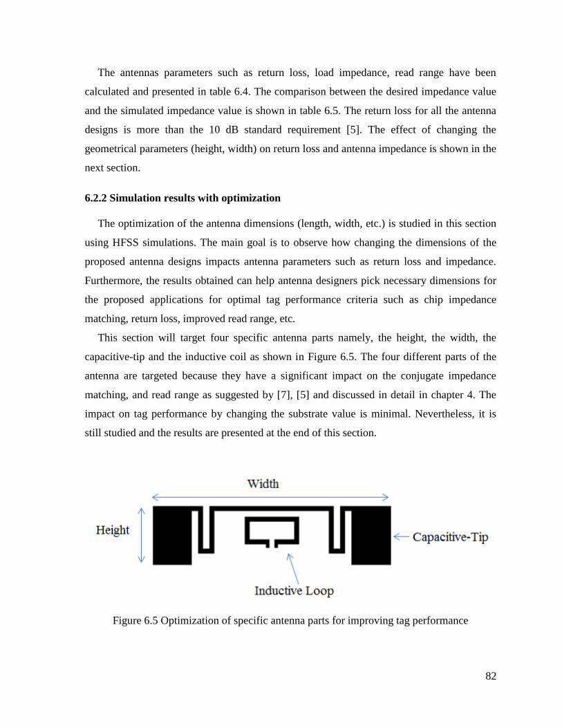
82
The antennas parameters such as return loss, load impedance, read range have been
calculated and presented in table 6.4. The comparison between the desired impedance value
and the simulated impedance value is shown in table 6.5. The return loss for all the antenna
designs is more than the 10 dB standard requirement [5]. The effect of changing the
geometrical parameters (height, width) on return loss and antenna impedance is shown in the
next section.
6.2.2 Simulation results with optimization
The optimization of the antenna dimensions (length, width, etc.) is studied in this section
using HFSS simulations. The main goal is to observe how changing the dimensions of the
proposed antenna designs impacts antenna parameters such as return loss and impedance.
Furthermore, the results obtained can help antenna designers pick necessary dimensions for
the proposed applications for optimal tag performance criteria such as chip impedance
matching, return loss, improved read range, etc.
This section will target four specific antenna parts namely, the height, the width, the
capacitive-tip and the inductive coil as shown in Figure 6.5. The four different parts of the
antenna are targeted because they have a significant impact on the conjugate impedance
matching, and read range as suggested by [7], [5] and discussed in detail in chapter 4. The
impact on tag performance by changing the substrate value is minimal. Nevertheless, it is
still studied and the results are presented at the end of this section.
Figure 6.5 Optimization of specific antenna parts for improving tag performance
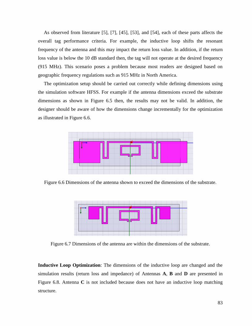
83
As observed from literature [5], [7], [45], [53], and [54], each of these parts affects the
overall tag performance criteria. For example, the inductive loop shifts the resonant
frequency of the antenna and this may impact the return loss value. In addition, if the return
loss value is below the 10 dB standard then, the tag will not operate at the desired frequency
(915 MHz). This scenario poses a problem because most readers are designed based on
geographic frequency regulations such as 915 MHz in North America.
The optimization setup should be carried out correctly while defining dimensions using
the simulation software HFSS. For example if the antenna dimensions exceed the substrate
dimensions as shown in Figure 6.5 then, the results may not be valid. In addition, the
designer should be aware of how the dimensions change incrementally for the optimization
as illustrated in Figure 6.6.
Figure 6.6 Dimensions of the antenna shown to exceed the dimensions of the substrate.
Figure 6.7 Dimensions of the antenna are within the dimensions of the substrate.
Inductive Loop Optimization: The dimensions of the inductive loop are changed and the
simulation results (return loss and impedance) of Antennas A, B and D are presented in
Figure 6.8. Antenna C is not included because does not have an inductive loop matching
structure.

84
Figure 6.8a Simulation results showing the return loss of the antenna A after optimization of
the Inductive loop.
Figure 6.8b Simulation results showing the impedance of the antenna A after optimization of
the Inductive loop.
0.50 0.60 0.70 0.80 0.90 1.00 1.10 1.20Freq [GHz]
-35.00
-30.00
-25.00
-20.00
-15.00
-10.00
-5.00
dB
(S(1
,1))
Ansoft LLC HFSSDesign1Freq[GHz] vs Return Loss[dB]
m1
m2
m3
m4
m5
Curve Info
dB(S(1,1))Setup1 : Sw eep1cmm='1mm'
dB(S(1,1))Setup1 : Sw eep1cmm='2mm'
dB(S(1,1))Setup1 : Sw eep1cmm='3mm'
dB(S(1,1))Setup1 : Sw eep1cmm='4mm'
dB(S(1,1))Setup1 : Sw eep1cmm='5mm'
Name X Y
m1 0.9150 -18.8970
m2 0.9150 -20.4298
m3 0.9150 -23.0078
m4 0.9150 -25.0806
m5 0.9150 -29.0331
0.50 0.60 0.70 0.80 0.90 1.00 1.10 1.20Freq [GHz]
0.00
50.00
100.00
150.00
200.00
250.00
Imp
ed
an
ce
Ansoft LLC HFSSDesign1Freq[GHz] vs Impedance
m1
m2
m3
m4
m5
m6m7m8m9m10
Curve Info
im(Z(1,1))Setup1 : Sw eep1cmm='1mm'
im(Z(1,1))Setup1 : Sw eep1cmm='2mm'
im(Z(1,1))Setup1 : Sw eep1cmm='3mm'
im(Z(1,1))Setup1 : Sw eep1cmm='4mm'
im(Z(1,1))Setup1 : Sw eep1cmm='5mm'
re(Z(1,1))Setup1 : Sw eep1cmm='1mm'
re(Z(1,1))Setup1 : Sw eep1cmm='2mm'
Name X Y
m1 0.9150 177.9480
m2 0.9150 162.8450
m3 0.9150 148.0114
m4 0.9150 131.8999
m5 0.9150 120.1312
m6 0.9150 7.6049
m7 0.9150 6.9889
m8 0.9150 5.5095
m9 0.9150 4.3891
m10 0.9150 3.5473

85
Figure 6.8c Simulation results showing the return loss of the antenna B after optimization of
the Inductive loop.
Figure 6.8d Simulation results showing the impedance of the antenna B after optimization of
the Inductive loop.
0.50 0.60 0.70 0.80 0.90 1.00 1.10 1.20Freq [GHz]
-27.50
-25.00
-22.50
-20.00
-17.50
-15.00
-12.50
-10.00
-7.50
dB
(S(1
,1))
Ansoft LLC HFSSDesign1Freq[GHz] vs Impedance
m1
m2
m3
m4
m5
Curve Info
dB(S(1,1))Setup1 : Sw eep1amm='1mm'
dB(S(1,1))Setup1 : Sw eep1amm='2mm'
dB(S(1,1))Setup1 : Sw eep1amm='3mm'
dB(S(1,1))Setup1 : Sw eep1amm='4mm'
dB(S(1,1))Setup1 : Sw eep1amm='5mm'
Name X Y
m1 0.9150 -12.1017
m2 0.9150 -13.0099
m3 0.9150 -15.0131
m4 0.9150 -17.0884
m5 0.9150 -20.8098
0.50 0.60 0.70 0.80 0.90 1.00 1.10 1.20Freq [GHz]
0.00
50.00
100.00
150.00
200.00
250.00
300.00
350.00
Imp
ed
an
ce
Ansoft LLC HFSSDesign1Freq[GHz] vs Impedance
m1m2
m3
m4
m5
m6m7m8m9m10
Curve Info
im(Z(1,1))Setup1 : Sw eep1amm='1mm'
im(Z(1,1))Setup1 : Sw eep1amm='2mm'
im(Z(1,1))Setup1 : Sw eep1amm='3mm'
im(Z(1,1))Setup1 : Sw eep1amm='4mm'
im(Z(1,1))Setup1 : Sw eep1amm='5mm'
re(Z(1,1))Setup1 : Sw eep1amm='1mm'
re(Z(1,1))Setup1 : Sw eep1amm='2mm'
Name X Y
m1 0.9150 241.0896
m2 0.9150 228.6388
m3 0.9150 209.3189
m4 0.9150 193.8519
m5 0.9150 176.6268
m6 0.9150 46.0442
m7 0.9150 43.7379
m8 0.9150 34.6029
m9 0.9150 31.0188
m10 0.9150 24.2784

86
Figure 6.8e Simulation results showing the return loss of the antenna D after optimization of
the Inductive loop.
Figure 6.8f Simulation results showing the impedance of the antenna D after optimization of
the Inductive loop.
Figure 6.8 Simulation results of inductive loop optimization of the proposed antennas
As seen from the Figure 6.8, the inductive coil has a significant impact on the resonant
frequency of the antenna. In addition, the reactive part of the impedance changes more
0.50 0.60 0.70 0.80 0.90 1.00 1.10 1.20Freq [GHz]
-27.50
-25.00
-22.50
-20.00
-17.50
-15.00
-12.50
-10.00
-7.50
dB
(S(1
,1))
Ansoft LLC HFSSDesign1Frequency[GHz] vs RL[dB]
m1
m2
m3m4
m5
Curve Info
dB(S(1,1))Setup1 : Sw eep1cmm='1mm'
dB(S(1,1))Setup1 : Sw eep1cmm='2mm'
dB(S(1,1))Setup1 : Sw eep1cmm='3mm'
dB(S(1,1))Setup1 : Sw eep1cmm='4mm'
dB(S(1,1))Setup1 : Sw eep1cmm='5mm'
Name X Y
m1 0.9150 -11.5442
m2 0.9150 -12.7717
m3 0.9150 -16.6370
m4 0.9150 -16.8643
m5 0.9150 -19.7977
0.50 0.60 0.70 0.80 0.90 1.00 1.10 1.20Freq [GHz]
0.00
50.00
100.00
150.00
200.00
250.00
300.00
350.00
Imp
ed
an
ce
Ansoft LLC HFSSDesign1Freq[GHz] vs Impedance
m1
m2
m3m4
m5
m6m7m9m8m10
Curve Info
im(Z(1,1))Setup1 : Sw eep1cmm='4mm'
im(Z(1,1))Setup1 : Sw eep1cmm='5mm'
re(Z(1,1))Setup1 : Sw eep1cmm='1mm'
re(Z(1,1))Setup1 : Sw eep1cmm='2mm'
re(Z(1,1))Setup1 : Sw eep1cmm='3mm'
re(Z(1,1))Setup1 : Sw eep1cmm='4mm'
re(Z(1,1))Setup1 : Sw eep1cmm='5mm'
Name X Y
m1 0.9150 254.3825
m2 0.9150 236.2062
m3 0.9150 198.8965
m4 0.9150 197.4212
m5 0.9150 181.7265
m6 0.9150 7.7120
m7 0.9150 8.9273
m8 0.9150 10.1079
m9 0.9150 10.6685
m10 0.9150 12.7982
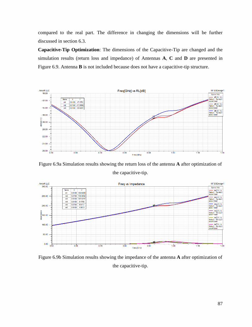
87
compared to the real part. The difference in changing the dimensions will be further
discussed in section 6.3.
Capacitive-Tip Optimization: The dimensions of the Capacitive-Tip are changed and the
simulation results (return loss and impedance) of Antennas A, C and D are presented in
Figure 6.9. Antenna B is not included because does not have a capacitive-tip structure.
Figure 6.9a Simulation results showing the return loss of the antenna A after optimization of
the capacitive-tip.
Figure 6.9b Simulation results showing the impedance of the antenna A after optimization of
the capacitive-tip.
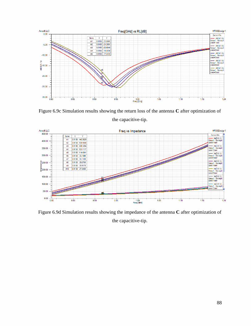
88
Figure 6.9c Simulation results showing the return loss of the antenna C after optimization of
the capacitive-tip.
Figure 6.9d Simulation results showing the impedance of the antenna C after optimization of
the capacitive-tip.

89
Figure 6.9e Simulation results showing the return loss of the antenna D after optimization of
the capacitive-tip.
Figure 6.9f Simulation results showing the impedance of the antenna C after optimization of
the capacitive-tip.
Figure 6.9 Simulation results of capacitive tip optimization of the proposed antennas
As seen from the Figure 6.9, the capacitive-tip has an impact on the impedance of the
antenna. In addition, the resonant frequency does not change by changing the dimensions of
the capacitive-tip. The difference in changing the dimensions will be further discussed in the
section 6.3.

90
Antenna - Height Optimization: The dimensions of the antenna height are changed and the
simulation results (return loss and impedance) of Antennas A, B, C and D are presented in
Figure 6.10.
Figure 6.10a Simulation results showing the return loss of the antenna A after optimization
of the height of the antenna.
Figure 6.10b Simulation results showing the impedance of the antenna A after optimization
of the height of the antenna.

91
Figure 6.10c Simulation results showing the return loss of the antenna B after optimization
of the height of the antenna.
Figure 6.10d Simulation results showing the impedance of the antenna B after optimization
of the height of the antenna.
0.50 0.60 0.70 0.80 0.90 1.00 1.10 1.20Freq [GHz]
-27.50
-25.00
-22.50
-20.00
-17.50
-15.00
-12.50
-10.00
dB
(S(1
,1))
Ansoft LLC HFSSDesign1Freq[GHz] vs RL[dB]1
m1
m2m3m4
m5
Curve Info
dB(S(1,1))Setup1 : Sw eep1bmm='1mm'
dB(S(1,1))Setup1 : Sw eep1bmm='2mm'
dB(S(1,1))Setup1 : Sw eep1bmm='3mm'
dB(S(1,1))Setup1 : Sw eep1bmm='4mm'
dB(S(1,1))Setup1 : Sw eep1bmm='5mm'
Name X Y
m1 0.9150 -19.5347
m2 0.9150 -20.2546
m3 0.9150 -20.4426
m4 0.9150 -20.4959
m5 0.9150 -21.2803
0.50 0.60 0.70 0.80 0.90 1.00 1.10 1.20Freq [GHz]
0.00
50.00
100.00
150.00
200.00
250.00
Imp
ed
an
ce
Ansoft LLC HFSSDesign1Freq[GHz] vs Impedance1
m1m2m3m4m5
m6m7m8m9m10
Curve Info
im(Z(1,1))Setup1 : Sw eep1bmm='1mm'
im(Z(1,1))Setup1 : Sw eep1bmm='2mm'
im(Z(1,1))Setup1 : Sw eep1bmm='3mm'
im(Z(1,1))Setup1 : Sw eep1bmm='4mm'
im(Z(1,1))Setup1 : Sw eep1bmm='5mm'
re(Z(1,1))Setup1 : Sw eep1bmm='1mm'
re(Z(1,1))Setup1 : Sw eep1bmm='2mm'
Name X Y
m1 0.9150 183.0474
m2 0.9150 176.9602
m3 0.9150 176.8097
m4 0.9150 176.3501
m5 0.9150 174.7055
m6 0.9150 14.6030
m7 0.9150 7.8427
m8 0.9150 5.6308
m9 0.9150 3.7571
m10 0.9150 3.0251

92
Figure 6.10e Simulation results showing the return loss of the antenna C after optimization
of the height of the antenna.
Figure 6.10f Simulation results showing the impedance of the antenna C after optimization
of the height of the antenna.
0.80 0.85 0.90 0.95 1.00 1.05 1.10 1.15 1.20Freq [GHz]
-25.00
-20.00
-15.00
-10.00
-5.00
0.00
dB
(S(1
,1))
Ansoft LLC HFSSDesign1Freq[GHz] vs RL[dB]
m1
m2
m3
m4
m5
Curve Info
dB(S(1,1))Setup1 : Sw eep1bmm='1mm'
dB(S(1,1))Setup1 : Sw eep1bmm='2mm'
dB(S(1,1))Setup1 : Sw eep1bmm='3mm'
dB(S(1,1))Setup1 : Sw eep1bmm='4mm'
dB(S(1,1))Setup1 : Sw eep1bmm='5mm'
Name X Y
m1 0.9150 -12.9461
m2 0.9150 -14.2318
m3 0.9150 -15.7701
m4 0.9150 -19.8844
m5 0.9150 -22.5222
0.80 0.85 0.90 0.95 1.00 1.05 1.10 1.15 1.20Freq [GHz]
0.00
50.00
100.00
150.00
200.00
250.00
300.00
350.00
400.00
450.00
Imp
ed
an
ce
Ansoft LLC HFSSDesign1Freq[GHz] vs Impedance
m1m2
m3m4m5
m6
Curve Info
im(Z(1,1))Setup1 : Sw eep1bmm='1mm'
im(Z(1,1))Setup1 : Sw eep1bmm='2mm'
im(Z(1,1))Setup1 : Sw eep1bmm='3mm'
im(Z(1,1))Setup1 : Sw eep1bmm='4mm'
im(Z(1,1))Setup1 : Sw eep1bmm='5mm'
re(Z(1,1))Setup1 : Sw eep1bmm='1mm'
re(Z(1,1))Setup1 : Sw eep1bmm='2mm'
Name X Y
m1 0.9150 135.7685
m2 0.9150 125.2113
m3 0.9150 108.4751
m4 0.9150 100.9883
m5 0.9150 94.2487
m6 0.9150 30.3714

93
Figure 6.10g Simulation results showing the return loss of the antenna D after optimization
of the height of the antenna.
Figure 6.10h Simulation results showing the impedance of the antenna D after optimization
of the height of the antenna.
Figure 6.10 Simulation results of height optimization of the proposed antennas
As seen from the Figure 6.10, the height of the antenna structures has an impact on the
reactive part of the impedance at the desired frequency of 915 MHz. In addition, the resonant
frequency is not affected by changing the height of the antenna designs. The difference in
changing the dimensions will be further discussed in the section 6.3.
0.50 0.60 0.70 0.80 0.90 1.00 1.10 1.20Freq [GHz]
-27.50
-25.00
-22.50
-20.00
-17.50
-15.00
-12.50
-10.00
dB
(S(1
,1))
Ansoft LLC HFSSDesign1Frequency[GHz] vs RL[dB]
m1m2
m3m4m5
Curve Info
dB(S(1,1))Setup1 : Sw eep1bmm='1mm'
dB(S(1,1))Setup1 : Sw eep1bmm='2mm'
dB(S(1,1))Setup1 : Sw eep1bmm='3mm'
dB(S(1,1))Setup1 : Sw eep1bmm='4mm'
dB(S(1,1))Setup1 : Sw eep1bmm='5mm'
Name X Y
m1 0.9150 -19.1305
m2 0.9150 -19.3059
m3 0.9150 -20.2789
m4 0.9150 -20.2890
m5 0.9150 -20.7970
0.50 0.60 0.70 0.80 0.90 1.00 1.10 1.20Freq [GHz]
0.00
50.00
100.00
150.00
200.00
250.00
Imp
ed
an
ce
Ansoft LLC HFSSDesign1Freq[GHz] vs Impedance
m1m2m3m4m5
m6m7m8m9m10
Curve Info
im(Z(1,1))Setup1 : Sw eep1bmm='1mm'
im(Z(1,1))Setup1 : Sw eep1bmm='2mm'
im(Z(1,1))Setup1 : Sw eep1bmm='3mm'
im(Z(1,1))Setup1 : Sw eep1bmm='4mm'
im(Z(1,1))Setup1 : Sw eep1bmm='5mm'
re(Z(1,1))Setup1 : Sw eep1bmm='1mm'
re(Z(1,1))Setup1 : Sw eep1bmm='2mm'
Name X Y
m1 0.9150 177.7792
m2 0.9150 184.8419
m3 0.9150 182.9687
m4 0.9150 177.9110
m5 0.9150 177.3787
m6 0.9150 18.5538
m7 0.9150 13.4214
m8 0.9150 7.6931
m9 0.9150 5.8220
m10 0.9150 4.4386

94
Antenna - Width Optimization: The dimensions of the antenna width are changed and the
simulation results (return loss and impedance) of Antennas A, B, C and D are presented in
Figure 6.11.
Figure 6.11a Simulation results showing the return loss of the antenna A after optimization
of the width of the antenna.
Figure 6.11b Simulation results showing the impedance of the antenna A after optimization
of the width of the antenna.

95
Figure 6.11c Simulation results showing the return loss of the antenna B after optimization
of the width of the antenna.
Figure 6.11d Simulation results showing the impedance of the antenna B after optimization
of the width of the antenna.
0.50 0.60 0.70 0.80 0.90 1.00 1.10 1.20Freq [GHz]
-27.50
-25.00
-22.50
-20.00
-17.50
-15.00
-12.50
-10.00
-7.50
-5.00
dB
(S(1
,1))
Ansoft LLC HFSSDesign1Freq[GHz] vs RL[dB]
m1
m2
m3
m4
m5
Curve Info
dB(S(1,1))Setup1 : Sw eep1amm='1mm'
dB(S(1,1))Setup1 : Sw eep1amm='2mm'
dB(S(1,1))Setup1 : Sw eep1amm='3mm'
dB(S(1,1))Setup1 : Sw eep1amm='4mm'
dB(S(1,1))Setup1 : Sw eep1amm='5mm'
Name X Y
m1 0.9150 -12.1488
m2 0.9150 -13.5096
m3 0.9150 -15.1635
m4 0.9150 -16.1694
m5 0.9150 -18.4684
0.50 0.60 0.70 0.80 0.90 1.00 1.10 1.20Freq [GHz]
0.00
125.00
250.00
375.00
Imp
ed
an
ce
Ansoft LLC HFSSDesign1Freq[GHz] vs Impedance
m1
m2
m3m4
m5
m6m7
Curve Info
im(Z(1,1))Setup1 : Sw eep1amm='1mm'
im(Z(1,1))Setup1 : Sw eep1amm='2mm'
im(Z(1,1))Setup1 : Sw eep1amm='3mm'
im(Z(1,1))Setup1 : Sw eep1amm='4mm'
im(Z(1,1))Setup1 : Sw eep1amm='5mm'
re(Z(1,1))Setup1 : Sw eep1amm='1mm'
re(Z(1,1))Setup1 : Sw eep1amm='2mm'
Name X Y
m1 0.9150 243.8667
m2 0.9150 225.6988
m3 0.9150 208.6276
m4 0.9150 201.9911
m5 0.9150 187.8276
m6 0.9150 10.6563
m7 0.9150 8.3515
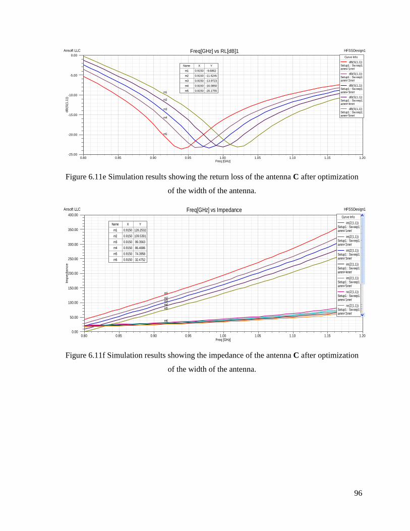
96
Figure 6.11e Simulation results showing the return loss of the antenna C after optimization
of the width of the antenna.
Figure 6.11f Simulation results showing the impedance of the antenna C after optimization
of the width of the antenna.
0.80 0.85 0.90 0.95 1.00 1.05 1.10 1.15 1.20Freq [GHz]
-25.00
-20.00
-15.00
-10.00
-5.00
0.00
dB
(S(1
,1))
Ansoft LLC HFSSDesign1Freq[GHz] vs RL[dB]1
m1
m2
m3
m4
m5
Curve Info
dB(S(1,1))Setup1 : Sw eep1amm='1mm'
dB(S(1,1))Setup1 : Sw eep1amm='2mm'
dB(S(1,1))Setup1 : Sw eep1amm='3mm'
dB(S(1,1))Setup1 : Sw eep1amm='4mm'
dB(S(1,1))Setup1 : Sw eep1amm='5mm'
Name X Y
m1 0.9150 -9.6862
m2 0.9150 -11.6245
m3 0.9150 -13.9723
m4 0.9150 -16.0850
m5 0.9150 -20.1755
0.80 0.85 0.90 0.95 1.00 1.05 1.10 1.15 1.20Freq [GHz]
0.00
50.00
100.00
150.00
200.00
250.00
300.00
350.00
400.00
Imp
ed
an
ce
Ansoft LLC HFSSDesign1Freq[GHz] vs Impedance
m1
m2m3m4m5
m6
Curve Info
im(Z(1,1))Setup1 : Sw eep1amm='1mm'
im(Z(1,1))Setup1 : Sw eep1amm='2mm'
im(Z(1,1))Setup1 : Sw eep1amm='3mm'
im(Z(1,1))Setup1 : Sw eep1amm='4mm'
im(Z(1,1))Setup1 : Sw eep1amm='5mm'
re(Z(1,1))Setup1 : Sw eep1amm='1mm'
re(Z(1,1))Setup1 : Sw eep1amm='2mm'
Name X Y
m1 0.9150 126.2532
m2 0.9150 109.5391
m3 0.9150 99.3563
m4 0.9150 86.4686
m5 0.9150 74.3958
m6 0.9150 32.4752

97
Figure 6.11g Simulation results showing the return loss of the antenna D after optimization
of the width of the antenna.
Figure 6.11h Simulation results showing the impedance of the antenna D after optimization
of the width of the antenna.
Figure 6.11 Simulation results of width optimization of the proposed antennas.
As seen from the Figure 6.11, the width of the antenna structures has an impact on the
real part of the impedance at the desired frequency of 915 MHz. In addition, the resonant
frequency is not affected by changing the height of the antenna designs. The difference in
changing the dimensions will be further discussed in the section 6.3.
0.50 0.60 0.70 0.80 0.90 1.00 1.10 1.20Freq [GHz]
-27.50
-25.00
-22.50
-20.00
-17.50
-15.00
-12.50
-10.00
dB
(S(1
,1))
Ansoft LLC HFSSDesign1Frequency[GHz] vs RL[dB]
m1m2m3
m4
m5
Curve Info
dB(S(1,1))Setup1 : Sw eep1amm='1mm'
dB(S(1,1))Setup1 : Sw eep1amm='2mm'
dB(S(1,1))Setup1 : Sw eep1amm='3mm'
dB(S(1,1))Setup1 : Sw eep1amm='4mm'
dB(S(1,1))Setup1 : Sw eep1amm='5mm'
Name X Y
m1 0.9150 -18.8175
m2 0.9150 -18.5892
m3 0.9150 -18.6012
m4 0.9150 -19.7506
m5 0.9150 -18.4124
0.50 0.60 0.70 0.80 0.90 1.00 1.10 1.20Freq [GHz]
0.00
50.00
100.00
150.00
200.00
250.00
Imp
ed
an
ce
Ansoft LLC HFSSDesign1Freq[GHz] vs Impedance
m1m2m3m4m5
m6m7m8m9m10
Curve Info
im(Z(1,1))Setup1 : Sw eep1amm='4mm'
im(Z(1,1))Setup1 : Sw eep1amm='5mm'
re(Z(1,1))Setup1 : Sw eep1amm='1mm'
re(Z(1,1))Setup1 : Sw eep1amm='2mm'
re(Z(1,1))Setup1 : Sw eep1amm='3mm'
re(Z(1,1))Setup1 : Sw eep1amm='4mm'
re(Z(1,1))Setup1 : Sw eep1amm='5mm'
Name X Y
m1 0.9150 186.3735
m2 0.9150 187.6407
m3 0.9150 187.1451
m4 0.9150 180.8561
m5 0.9150 187.2385
m6 0.9150 19.4573
m7 0.9150 15.0558
m8 0.9150 10.7464
m9 0.9150 7.5316
m10 0.9150 6.6429
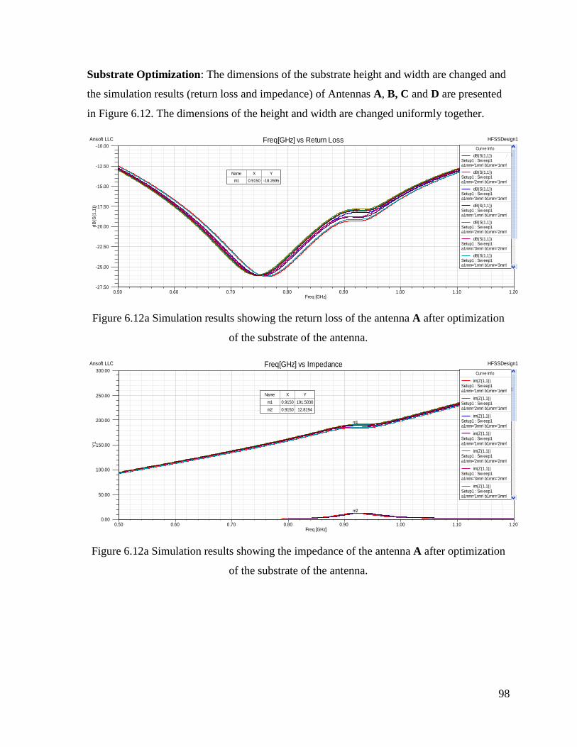
98
Substrate Optimization: The dimensions of the substrate height and width are changed and
the simulation results (return loss and impedance) of Antennas A, B, C and D are presented
in Figure 6.12. The dimensions of the height and width are changed uniformly together.
Figure 6.12a Simulation results showing the return loss of the antenna A after optimization
of the substrate of the antenna.
Figure 6.12a Simulation results showing the impedance of the antenna A after optimization
of the substrate of the antenna.
0.50 0.60 0.70 0.80 0.90 1.00 1.10 1.20Freq [GHz]
-27.50
-25.00
-22.50
-20.00
-17.50
-15.00
-12.50
-10.00
dB
(S(1
,1))
Ansoft LLC HFSSDesign1Freq[GHz] vs Return Loss
m1
Curve Info
dB(S(1,1))Setup1 : Sw eep1a1mm='1mm' b1mm='1mm'
dB(S(1,1))Setup1 : Sw eep1a1mm='2mm' b1mm='1mm'
dB(S(1,1))Setup1 : Sw eep1a1mm='3mm' b1mm='1mm'
dB(S(1,1))Setup1 : Sw eep1a1mm='1mm' b1mm='2mm'
dB(S(1,1))Setup1 : Sw eep1a1mm='2mm' b1mm='2mm'
dB(S(1,1))Setup1 : Sw eep1a1mm='3mm' b1mm='2mm'
dB(S(1,1))Setup1 : Sw eep1a1mm='1mm' b1mm='3mm'
Name X Y
m1 0.9150 -18.2695
0.50 0.60 0.70 0.80 0.90 1.00 1.10 1.20Freq [GHz]
0.00
50.00
100.00
150.00
200.00
250.00
300.00
Y1
Ansoft LLC HFSSDesign1Freq[GHz] vs Impedance
m1
m2
Curve Info
im(Z(1,1))Setup1 : Sw eep1a1mm='1mm' b1mm='1mm'
im(Z(1,1))Setup1 : Sw eep1a1mm='2mm' b1mm='1mm'
im(Z(1,1))Setup1 : Sw eep1a1mm='3mm' b1mm='1mm'
im(Z(1,1))Setup1 : Sw eep1a1mm='1mm' b1mm='2mm'
im(Z(1,1))Setup1 : Sw eep1a1mm='2mm' b1mm='2mm'
im(Z(1,1))Setup1 : Sw eep1a1mm='3mm' b1mm='2mm'
im(Z(1,1))Setup1 : Sw eep1a1mm='1mm' b1mm='3mm'
Name X Y
m1 0.9150 191.5030
m2 0.9150 12.8194
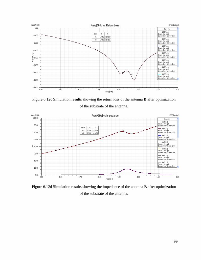
99
Figure 6.12c Simulation results showing the return loss of the antenna B after optimization
of the substrate of the antenna.
Figure 6.12d Simulation results showing the impedance of the antenna B after optimization
of the substrate of the antenna.
0.50 0.60 0.70 0.80 0.90 1.00 1.10 1.20Freq [GHz]
-45.00
-40.00
-35.00
-30.00
-25.00
-20.00
-15.00
-10.00
-5.00
dB
(S(1
,1))
Ansoft LLC HFSSDesign1Freq [GHz] vs Return Loss
m1m2
Curve Info
dB(S(1,1))Setup1 : Sw eep1$a1mm='1mm' $b1mm='1mm'
dB(S(1,1))Setup1 : Sw eep1$a1mm='2mm' $b1mm='1mm'
dB(S(1,1))Setup1 : Sw eep1$a1mm='3mm' $b1mm='1mm'
dB(S(1,1))Setup1 : Sw eep1$a1mm='1mm' $b1mm='2mm'
dB(S(1,1))Setup1 : Sw eep1$a1mm='2mm' $b1mm='2mm'
dB(S(1,1))Setup1 : Sw eep1$a1mm='3mm' $b1mm='2mm'
dB(S(1,1))Setup1 : Sw eep1$a1mm='1mm' $b1mm='3mm'
Name X Y
m1 0.9150 -35.6883
m2 0.9600 -36.7811
0.50 0.60 0.70 0.80 0.90 1.00 1.10 1.20Freq [GHz]
0.00
25.00
50.00
75.00
100.00
125.00
150.00
175.00
200.00
Y1
Ansoft LLC HFSSDesign1Freq[GHz] vs Impedance
m1
m2
Curve Info
im(Z(1,1))Setup1 : Sw eep1$a1mm='1mm' $b1mm='1mm'
im(Z(1,1))Setup1 : Sw eep1$a1mm='2mm' $b1mm='1mm'
im(Z(1,1))Setup1 : Sw eep1$a1mm='3mm' $b1mm='1mm'
im(Z(1,1))Setup1 : Sw eep1$a1mm='1mm' $b1mm='2mm'
im(Z(1,1))Setup1 : Sw eep1$a1mm='2mm' $b1mm='2mm'
im(Z(1,1))Setup1 : Sw eep1$a1mm='3mm' $b1mm='2mm'
im(Z(1,1))Setup1 : Sw eep1$a1mm='1mm' $b1mm='3mm'
Name X Y
m1 0.9150 152.8996
m2 0.9150 16.8486

100
Figure 6.12e Simulation results showing the return loss of the antenna C after optimization
of the substrate of the antenna.
Figure 6.12f Simulation results showing the impedance of the antenna C after optimization
of the substrate of the antenna.
0.80 0.85 0.90 0.95 1.00 1.05 1.10 1.15 1.20Freq [GHz]
-25.00
-22.50
-20.00
-17.50
-15.00
-12.50
-10.00
-7.50
-5.00
dB
(S(1
,1))
Ansoft LLC HFSSDesign1Freq[GHz] vs Return Loss
m1
Curve Info
dB(S(1,1))Setup1 : Sw eep1$a1mm='3mm' $b1mm='1mm'
dB(S(1,1))Setup1 : Sw eep1$a1mm='1mm' $b1mm='2mm'
dB(S(1,1))Setup1 : Sw eep1$a1mm='2mm' $b1mm='2mm'
dB(S(1,1))Setup1 : Sw eep1$a1mm='3mm' $b1mm='2mm'
dB(S(1,1))Setup1 : Sw eep1$a1mm='1mm' $b1mm='3mm'
dB(S(1,1))Setup1 : Sw eep1$a1mm='2mm' $b1mm='3mm'
dB(S(1,1))Setup1 : Sw eep1$a1mm='3mm' $b1mm='3mm'
Name X Y
m1 0.9150 -23.8251
0.80 0.85 0.90 0.95 1.00 1.05 1.10 1.15 1.20Freq [GHz]
0.00
100.00
200.00
300.00
400.00
500.00
Y1
Ansoft LLC HFSSDesign1Freq[GHz] vs Impedance
m1
m2
Curve Info
im(Z(1,1))Setup1 : Sw eep1$a1mm='1mm' $b1mm='1mm'
im(Z(1,1))Setup1 : Sw eep1$a1mm='2mm' $b1mm='1mm'
im(Z(1,1))Setup1 : Sw eep1$a1mm='3mm' $b1mm='1mm'
im(Z(1,1))Setup1 : Sw eep1$a1mm='1mm' $b1mm='2mm'
im(Z(1,1))Setup1 : Sw eep1$a1mm='2mm' $b1mm='2mm'
im(Z(1,1))Setup1 : Sw eep1$a1mm='3mm' $b1mm='2mm'
im(Z(1,1))Setup1 : Sw eep1$a1mm='1mm' $b1mm='3mm'
Name X Y
m1 0.9150 146.2878
m2 0.9150 34.7018

101
Figure 6.12g Simulation results showing the return loss of the antenna D after optimization
of the substrate of the antenna.
Figure 6.12h Simulation results showing the return loss of the antenna D after optimization
of the substrate of the antenna.
Figure 6.12 Simulation results of substrate optimization of the proposed antennas
As seen from the Figure 6.12, changing the dimensions of the substrate has a minimal
impact on the return loss and the impedance of the antenna designs.
0.50 0.60 0.70 0.80 0.90 1.00 1.10 1.20Freq [GHz]
-45.00
-40.00
-35.00
-30.00
-25.00
-20.00
-15.00
-10.00
-5.00
dB
(S(1
,1))
Ansoft LLC HFSSDesign1Freq[GHz] vs Return Loss
m1
m2
Curve Info
dB(S(1,1))Setup1 : Sw eep1$a1='1mm' $b1='1mm'
dB(S(1,1))Setup1 : Sw eep1$a1='2mm' $b1='1mm'
dB(S(1,1))Setup1 : Sw eep1$a1='3mm' $b1='1mm'
dB(S(1,1))Setup1 : Sw eep1$a1='1mm' $b1='2mm'
dB(S(1,1))Setup1 : Sw eep1$a1='2mm' $b1='2mm'
dB(S(1,1))Setup1 : Sw eep1$a1='3mm' $b1='2mm'
dB(S(1,1))Setup1 : Sw eep1$a1='1mm' $b1='3mm'
Name X Y
m1 0.9150 -32.5783
m2 0.9600 -44.2656
0.50 0.60 0.70 0.80 0.90 1.00 1.10 1.20Freq [GHz]
0.00
25.00
50.00
75.00
100.00
125.00
150.00
175.00
200.00
225.00
Y1
Ansoft LLC HFSSDesign1Freq[GHz] vs Impedance
m1
m2
Curve Info
im(Z(1,1))Setup1 : Sw eep1$a1='1mm' $b1='1mm'
im(Z(1,1))Setup1 : Sw eep1$a1='2mm' $b1='1mm'
im(Z(1,1))Setup1 : Sw eep1$a1='3mm' $b1='1mm'
im(Z(1,1))Setup1 : Sw eep1$a1='1mm' $b1='2mm'
im(Z(1,1))Setup1 : Sw eep1$a1='2mm' $b1='2mm'
im(Z(1,1))Setup1 : Sw eep1$a1='3mm' $b1='2mm'
im(Z(1,1))Setup1 : Sw eep1$a1='1mm' $b1='3mm'
Name X Y
m1 0.9150 152.7535
m2 0.9150 21.3036

102
6.3 Discussion of Simulation Results
All the antenna designs except antenna design E were simulated using HFSS. The results
show that changing the dimensions of the proposed antenna impacts antenna parameters
such as return loss and impedance. Furthermore, the results obtained can help antenna
designers pick necessary dimensions for the proposed applications for optimal tag
performance criteria such as chip impedance matching, return loss, improved read range, etc.
The optimization results show that the substrate has a minimal impact on the return loss
and the impedance of the antenna designs. This effect of the four specific antenna parts
namely, the height, the width, the capacitive-tip and the inductive coil are listed in table 6.6.
Table 6.6 The effect of antenna designs parts on return loss and impedance after
optimization.
Antenna Inductive loop Capacitive-Tip Height Width
A Significant Impact
on return loss
Minimal impact on
impedance
Minimal impact on
impedance
Minimal
impact on
impedance
B Significant Impact
on return loss
None (no capacitve-
tip)
Real part of
impedance
Imaginary part
of impedance
C None (no loop) Improves return loss
and impedance
Return loss and
Imaginary
impedance
Return loss
and Imaginary
impedance
D Significant Impact
on return loss
Improves return loss
only
Real part of
impedance
Imaginary part
of impedance
After the optimization process, the final antenna design dimensions proposed for each
antenna are listed in table 6.7
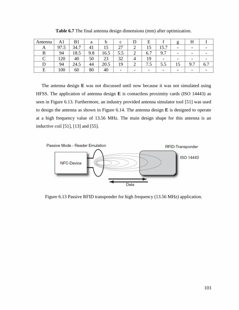
103
Table 6.7 The final antenna design dimensions (mm) after optimization.
Antenna A1 B1 a b c D E f g H I
A 97.5 34.7 41 15 27 2 15 15.7 - - -
B 94 18.5 9.8 16.5 5.5 2 6.7 9.7 - - -
C 120 40 50 23 32 4 19 - - - -
D 94 24.5 44 20.5 19 2 7.5 5.5 15 9.7 6.7
E 100 60 80 40 - - - - - - -
The antenna design E was not discussed until now because it was not simulated using
HFSS. The application of antenna design E is contactless proximity cards (ISO 14443) as
seen in Figure 6.13. Furthermore, an industry provided antenna simulator tool [51] was used
to design the antenna as shown in Figure 6.14. The antenna design E is designed to operate
at a high frequency value of 13.56 MHz. The main design shape for this antenna is an
inductive coil [51], [13] and [55].
Figure 6.13 Passive RFID transponder for high frequency (13.56 MHz) application.

104
Figure 6.14 Inductive coil antenna design for high frequency (13.56 MHz) application.
As proposed by [4] equation (21), the impedance matching is achieved by calculating the
right antenna coil inductance.
( ) ( )
In equation (21) [52], is 13.56 MHz and is 17pF. Therefore, the required
inductance value after using the antenna simulator is found to be 8.092 nH.The chip chosen
for this application is the NXP Mifare and has an impedance of 17 pF. In order, to match this
impedance the inductance value obtained should be 8.103 nH.
6.4 Chapter Summary
In this chapter the simulation results of the designed tags based on the application of use
were presented. The simulation software HFSS was used to optimize the dimensions of the
proposed antenna. The different antenna designs (A, B, C, D and E) and the advantages of
using the particular geometry were discussed. The results show the impact of changing the

105
dimensions on antenna parameters such as return loss and impedance. Furthermore, the
results obtained can help antenna designers pick necessary dimensions for the proposed
applications for optimal tag performance criteria such as chip impedance matching, return
loss, improved read range, etc. The parametric study and optimization of the proposed
designs were achieved using the FEM design tool. The simulations results provided help
select the best possible geometric dimensions for the proposed antennas before the actual
fabrications process. Therefore, the RF designers can be confident in the tag antenna design
before the fabrication process, thereby assuring a low cost solution to RFID system. Finally,
antenna design E was discussed briefly as it involves high frequency (13.56 MHz)
applications such as contactless cards.
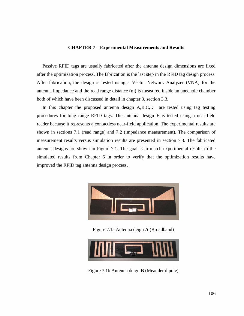
106
CHAPTER 7 – Experimental Measurements and Results
Passive RFID tags are usually fabricated after the antenna design dimensions are fixed
after the optimization process. The fabrication is the last step in the RFID tag design process.
After fabrication, the design is tested using a Vector Network Analyzer (VNA) for the
antenna impedance and the read range distance (m) is measured inside an anechoic chamber
both of which have been discussed in detail in chapter 3, section 3.3.
In this chapter the proposed antenna design A,B,C,D are tested using tag testing
procedures for long range RFID tags. The antenna design E is tested using a near-field
reader because it represents a contactless near-field application. The experimental results are
shown in sections 7.1 (read range) and 7.2 (impedance measurement). The comparison of
measurement results versus simulation results are presented in section 7.3. The fabricated
antenna designs are shown in Figure 7.1. The goal is to match experimental results to the
simulated results from Chapter 6 in order to verify that the optimization results have
improved the RFID tag antenna design process.
Figure 7.1a Antenna deign A (Broadband)
Figure 7.1b Antenna deign B (Meander dipole)

107
Figure 7.1c Antenna deign C (Two-Wire folded dipole)
Figure 7.1d Antenna deign D (Baggage tag dipole)
Figure 7.1e Antenna deign E (Contactless card)
Figure 7.1 Pictures of the fabricated antenna designs
7.1 Read Range
The read range distance measurement for RFID tags was carried out in an anechoic
chamber. The tags are placed at a fixed distance of 5 meters from the reader as seen in
Figure 7.2a, 7.2b. The frequency of interest is 915 MHz and the RFID reader used is
Convergence Systems Limited CSL CS203. The power of the reader was set to 30 dbm and
the read-count was observed on the computer attached to the reader.
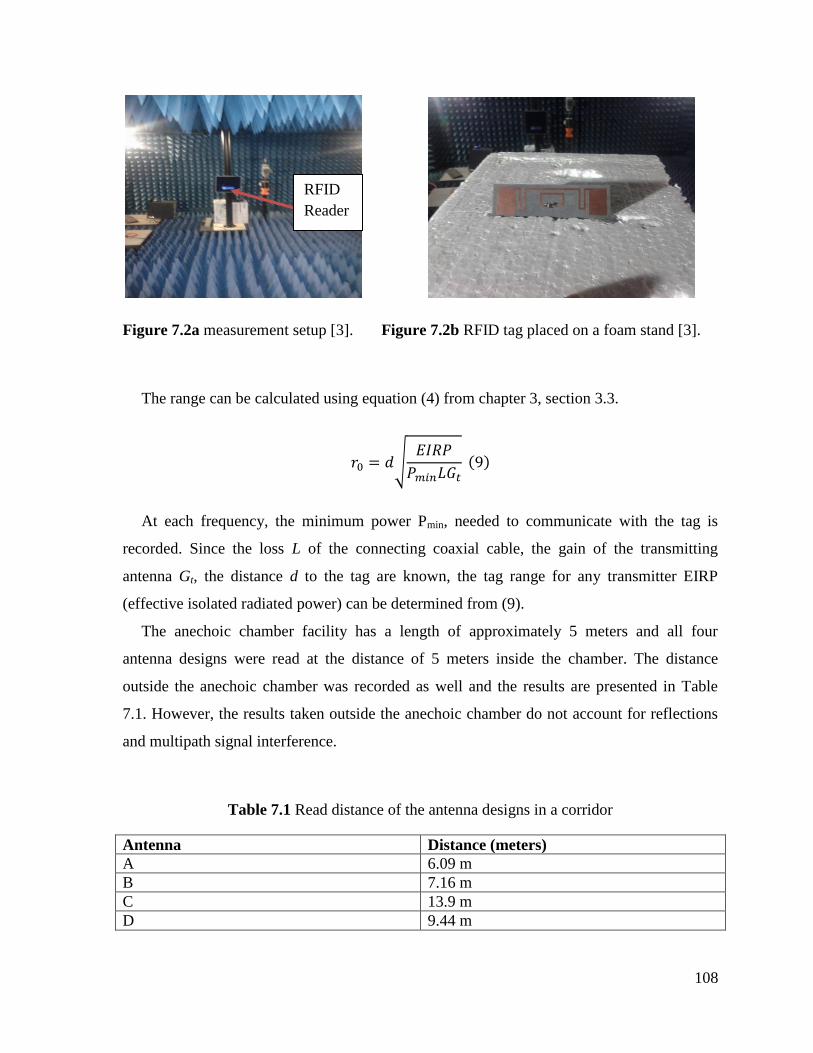
108
Figure 7.2a measurement setup [3]. Figure 7.2b RFID tag placed on a foam stand [3].
The range can be calculated using equation (4) from chapter 3, section 3.3.
√
( )
At each frequency, the minimum power Pmin, needed to communicate with the tag is
recorded. Since the loss L of the connecting coaxial cable, the gain of the transmitting
antenna Gt, the distance d to the tag are known, the tag range for any transmitter EIRP
(effective isolated radiated power) can be determined from (9).
The anechoic chamber facility has a length of approximately 5 meters and all four
antenna designs were read at the distance of 5 meters inside the chamber. The distance
outside the anechoic chamber was recorded as well and the results are presented in Table
7.1. However, the results taken outside the anechoic chamber do not account for reflections
and multipath signal interference.
Table 7.1 Read distance of the antenna designs in a corridor
Antenna Distance (meters)
A 6.09 m
B 7.16 m
C 13.9 m
D 9.44 m
RFID
Reader
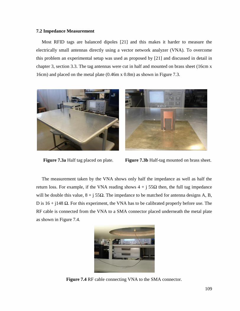
109
7.2 Impedance Measurement
Most RFID tags are balanced dipoles [21] and this makes it harder to measure the
electrically small antennas directly using a vector network analyzer (VNA). To overcome
this problem an experimental setup was used as proposed by [21] and discussed in detail in
chapter 3, section 3.3. The tag antennas were cut in half and mounted on brass sheet (16cm x
16cm) and placed on the metal plate (0.46m x 0.8m) as shown in Figure 7.3.
Figure 7.3a Half tag placed on plate. Figure 7.3b Half-tag mounted on brass sheet.
The measurement taken by the VNA shows only half the impedance as well as half the
return loss. For example, if the VNA reading shows 4 + j 55Ω then, the full tag impedance
will be double this value, 8 + j 55Ω. The impedance to be matched for antenna designs A, B,
D is 16 + j148 Ω. For this experiment, the VNA has to be calibrated properly before use. The
RF cable is connected from the VNA to a SMA connector placed underneath the metal plate
as shown in Figure 7.4.
Figure 7.4 RF cable connecting VNA to the SMA connector.

110
The calibration of the VNA is a very important step. It is typically done with a 50 Ohm
balanced load. The results of the VNA calibration are shown in Figure 7.5.
Figure 7.5a Impedance of the VNA with a matched 50 Ohm load.
Figure 7.5b Return Loss of the VNA with a matched 50 Ohm load.

111
It was observed that the brass plate has minimal impact on the impedance value when
connected to the VNA. The results below show the return loss as well as the impedance for
the four antenna designs.
Figure 7.6a Impedance of Antenna A. Figure 7.6b Return Loss (dB) of Antenna A
Figure 7.6c Impedance of Antenna B. Figure 7.6d Return Loss (dB) of Antenna B

112
Figure 7.6f Impedance of Antenna C Figure 7.6g Return Loss (dB) of Antenna C
Figure 7.6h Impedance of Antenna D Figure 7.6i Return Loss (dB) of Antenna D
Figure 7.6 Measured impedance and return loss of the proposed antennas.
7.3 Comparison of simulated and measured results
This section provides the comparison of the measured versus the simulated results. The
impedance at 915 MHz of the antenna designs A, B, C and D and other antenna parameters
such as read range, gain and return loss are displayed in table 7.2.

113
Table 7.2 Simulated and measured results.
Antenna Simulated
Impedance
(Ohm)
Measured
Impedance
(Ohm)
Simulated
Return
Loss (dB)
Measured
Return
Loss (dB)
Theoretical
Read
Range
(m)
Measured
Read
Range
(m)
A 10.9 + j 180.9 Ω 9 + j 320 Ω 19.91 18.2 9.86 6.09
B 18.1 + j 146.5 Ω 20 + j 205 Ω 41.20 32.8 11.76 7.16
C 14.2 + j 141.2 Ω 34.6 + j 240 Ω 23.20 20.4 8.21 13.9
D 21.1 + j 148.5 Ω 15 + j 240 Ω 35.34 18.20 12.68 9.44
The results from the simulation and measurement show close agreement when comparing
the return loss (dB) values. Furthermore, it was observed that the RF cable when connected
to the 50 Ohm matched load showed perfect matching. However, the SMA connector
connected to the experimental table was found to show some discrepancy. Therefore, the
measured impedance values do not exactly match the simulated impedance values. In
addition, the simulation setup is not entirely the same as the experimental setup i.e. no table
or connector or large radiation boundary was modeled in the simulation. Nevertheless, the
measured results show very good read range values which indicates good tag performance
characteristics and satisfies the requirements of the application such as pharmaceutical,
clothing, inventory, etc.
The return loss graph for the simulated and measured values is shown in 7.7.

114
Figure 7.7a Return Loss (dB) of Antenna A
Figure 7.7b Return Loss (dB) of Antenna B

115
Figure 7.7c Return Loss (dB) of Antenna C
Figure 7.7d Return Loss (dB) of Antenna D
Figure 7.7 Measured results versus the simulation results for the proposed antennas.
The figure 7.7 shows the measured return loss values versus the simulation return loss
values for each of the antenna designs, A, B, C and D. As shown by [22] the return loss
values are simply doubled to indicate an approximate return loss value for the full antenna

116
i.e. not just half the antenna. The antenna design E was fabricated according to the theory
outlined for HF tags used for contactless cards as explained in chapter 6, section 6.3. The
Figure 7.8 shows the typical antenna design for the HF tag used for contactless cards.
Figure 7.8a Industry HF tag antenna design [55]. Figure 7.8b Fabricated Antenna E.
The typical application of the designs shown in figure 7.8 is proximity contactless cards.
The antenna design E used a Nxp Mifare chip with an impedance value of 17pf. The results
of using this card with a smartphone reader and the ‘nxp info’ mobile application is shown in
figure 7.9.
** TagInfo scan (version 1.30) 2012-04-17 04:44:44 **
# IC manufacturer: NXP Semiconductors # IC type: MIFARE Ultralight C (MF0ICU2) # NFC Forum NDEF-compliant tag: Type 2 Tag ----------------------------------------------- # NFC data set information: Current message size: 18 bytes Maximum message size: 137 bytes NFC data set access: Read & Write Can be made Read-Only # Text record: type: "T" encoding: UTF-8 lang: en text: "Hi Mohamed."
Figure 7.9a Mobile application ‘Tag Info’ used to read the contactless card with the
smartphone.

117
# Memory size: 192 bytes * 48 pages, with 4 bytes per page
-----------------------------------------------
# Technologies supported: ISO/IEC 14443-3 (Type A) compatible ISO/IEC 14443-2 (Type A) compatible
Figure 7.9b Mobile application ‘Tag Info’ used to read the contactless card with the
smartphone.
The antenna design E was designed to be read by similar devices and HF readers.
However, the design E did not function as intended because of the possible factors listed
below.
1) The thickness of the substrate was found to be greater than a typical plastic card such
as a credit card.
2) The coil structure on the antenna might be disconnected at specific locations.
Therefore, it needs to be thoroughly viewed using a microscope.
The separation of the inductive loop lines is 0.5mm and this makes it hard to fabricate
using techniques such as ‘etching’.
7.4 Chapter Summary
In this chapter the simulation results and the measured results of the proposed antennas
were compared. The results from simulation and measurement show close agreement when
comparing the return loss (dB) values as shown in table 7.2. In addition, the measurement
results for the impedance values were shown to match closely in terms of the real component
of the impedance. For antenna design E the application of use is contactless card.
Furthermore, the demonstration of the application of antenna design E is demonstrated in
figure 7.9. The fabricated antenna did not function as intended because of the thickness of
the substrate and the difficulties encountered in the fabrication process. However, the design
can be implemented with the help of industry RFID tag printers that are customized to print
tags of applications such as contactless cards.

118
Chapter 8 – Conclusion
This thesis demonstrated the RFID tag antenna design process for passive UHF RFID tags
(915 MHz) as well as passive HF RFID tags (13.56 MHz). Although RFID technologies
have become very popular in recent years, there is still a significant gap when it comes to
accurate design of tags based on specific application or use such as inventory, clothing,
pharmaceuticals, etc.
The main problem that antenna designers face is chip-impedance matching. This
matching is necessary for optimal tag performance characteristics such as read range,
antenna radiation, antenna efficiency, etc. Some impedance matching techniques have been
presented namely, T-match, inductively coupled loop and nested slot techniques.
Furthermore, optimization of the antenna dimensions with the help of commercial
electromagnetic (EM) simulation tools was successfully achieved. The proposed antenna
designs for specific applications were thus fabricated and tested.
The RFID antenna design process required necessary evaluation of the application of use.
For example, the tag designed for pharmaceutical products requires the tag to be in close
vicinity of liquids and can significantly impact tag performance characteristics such as read
range, antenna efficiency, etc. Furthermore, as discussed in this work, RF designers can
select the best geometrical dimensions of the antenna based on impedance-matching charts
for optimal tag performance. Furthermore, as highlighted in this document, multiple
applications (baggage tag, clothing, inventory, etc.) can use the same ASIC-chip with
different antenna geometry.
8.1 Contribution
The main contribution of this thesis is the systemization of the RFID antenna design
process for RF designers by providing techniques to develop application-specific passive
RFID tags. Currently, industry RFID design procedures give more attention to the
application requirements of the RFID tags by means of fabrication and measurement
procedures as shown in [10] rather than precise chip impedance matching process. This

119
thesis proposes to fill this gap by providing a systemized passive RFID tag antenna design
procedure. As an example of this process, tag antenna designs (A, B, C, D and E) were
achieved through simulations and tag performance measurements. Furthermore, the results
obtained help RF designers select optimal impedance-matching antenna dimensions before
the fabrication process. As a result, this process will significantly reduce the RFID tag
development costs.
8.2 Future work
After analyzing the simulated/experimental results and considering previous research
work in this area, there are many possible future extensions to the RFID antenna design. One
extension of this work is to find applications where the RFID tags are affected by the
surrounding environment such as metals, water, glass wine bottle, etc. Some RFID antenna
designs such as planar inverted-F (PIFA) configurations and microstrip antennas form a
partial solution to this problem. However, the PIFA and microstrip design increase the
overall cost of the tag.
Another possible extension of is the design of a dual UHF/HF RFID tag to incorporate
item level tagging as well as distance-read tracking. Furthermore, the dual band tags research
will give way to dual band readers and reduce the overall cost of the RFID system.

120
REFERENCES
[1] D. C. Wyld, RFID: The right frequency for the government. A research monograph
from the IBM Center for the Business of Government, 2005.
[2] D. Dobkin and T. Wandinger, "A Radio-Oriented Introduction to Radio Frequency
Identification," High Frequency Electronics, pp. 46-51, 2005.
[3] D. Dobkin, pp. 69: The RF in RFID: Passive UHF RFID in Practice. Oxford: Elsevier,
2007.
[4] G. De Vita, G. Iannaccone, “Design criteria for the RF section of UHF and microwave
passive RFID transponders”, IEEE Trans. on Microw. Theory and Tech., vol. 53(9),
pp. 2978-2990, Sept. 2005
[5] K.V.S. Rao, P.V. Nikitin, and S. Lam, "Antenna design for UHF RFID tags: a review
and a practical application," IEEE Trans. on Antennas and Propag., vol. 53, pp. 3870-
3876, Dec. 2005.
[6] P.V. Nikitin, et al. Power reflection coefficient analysis for complex impedances in
RFID tag design, IEEE Trans. on Microw. Theory and Tech., 53(9): 2712–2725, Dec.
2005
[7] G. Marrocco, “The Art of UHF RFID antenna design: impedance-matching and size-
reduction techniques”, IEEE Antennas and Propag. Mag., vol. 50, Issue. 1, pp. 66-79,
Feb 2008.
[8] J.W. Lee et al. Design Consideration of UHF RFID Tag for Increased Reading Range.
IEEE MTT-S Int. Microw. Symp. Digest, 2006. pp. 1588 – 1591. 20 November 2006
[9] Avery Dennison, UHF RFID Inlays, Internet: http//rfid.averydennison.com /product_
cat/uhf-rfid-inlays, Accessed, Nov. 5, 2011.
[10] M. Bolic, D. Simplot-Ryl, and I. Stojmenovic, RF Systems: Research Trends and
Challenges. Wiley Online Library: John Wiley & Sons, 2010.

121
[11] N.C. Karmakar, Handbook of smart antennas for RFID systems. John Wiley & Sons.
Hoboken, New Jersey, 2010.
[12] K. Finkenzeller, RFID Handbook, 3rd edition, John Wiley & Sons, Hoboken, NJ,
2010.
[13] M. Myer, M. Brown, S. Patadia, and S. Dua, Passport for Comptia RFID+
Certification, McGraw-Hill, New York, 2007.
[14] R. Mark, The History of RFID Technology [Online], Available: http://www.rfidjournal.
com/article/view/1338/1, accessed 20 February 2012.
[15] H. Stockman, “Communication by Means of Reflected Power”, Proc. of the IRE, vol.
36, pp.1196-1204, October 1948.
[16] EPC Global Home Page [Online], Available: http://www.gs1.org/epcglobal, accessed
20 February 2012.
[17] Class 1 Generation 2 UHF Air Interface Protocol Standard.
http://www.epcglobalinc.org /standards/. Accessed Nov 10, 2011.
[18] A. Petosa, Antennas and Arrays, Carleton University Course Notes, Sep. 2011.
[19] C. Balanis, Antenna Theory, 3rd edn. Chichester: John Wiley & Sons, Ltd, 2005.
[20] L.J. Chu, “Physical limitations of omni-directional antennas,” J. Applied Physics, vol.
19, pp. 1163–1175. 1948.
[21] Y. Tikhov, Y. Kim, Y.-H. Min, "Compact low cost antenna for passive RFID
transponder," IEEE Int. Symp. Antennas Prop., pp. 10 15-1018, 2006.
[22] G. Marrocco, "RFID antennas for the UHF remote monitoring of human subjects,"
IEEE Trans. Antennas Prop., vol. 55, pp. 1862-1870, 2007.
[23] Avery Dennison, UHF RFID Inlays, http//rfid.averydennison.com/product_cat/uhf-
rfid-inlays, Accessed in Oct. 13, 2011.
[24] T. Hu, C. Liu, Z. Wang, “Design and analysis of UHF tag antenna structure,” China-
Japan Joint Microw. Conf., pp. 1-4, 2011.
122
[25] J.W. Lee et al., “Design consideration of UHF RFID tag for increased reading range,”
IEEE MTT Int. Microw. Symp., pp. 1588-1591, 2006.
[26] High-Frequency Structure Simulator, HFSS v12, Pittsburgh, PA, USA.
[27] A.C. Polycarpou, Introduction to Finite Element Methods in Electromagnetics,
Arizona: Morgan & Claypool, 2006.
[28] H. Hirvonenen, P. Pursula, K. Jaakkola and K. Laukkanen, "Planar Inverted-F Antenna
for Radio Frequency Identification," Electronics Letters, 40, 14, July 2004, pp. 848-
850.
[29] L. Ukkonen, M. Schaffrath, J. A. Kataja, L. Sydanheimo and M. Kivikoski,
“Evolutionary RFID tag antenna design for pape industry applications,” Int. J. RFID
and App., vol. 1, 2006, pp. 107-122.
[30] G. Marrocco, "Body-matched antennas for wireless biometry," European Conf. on
Antennas and Propag.Nice, France, p. 795, 2006.
[31] G. Marrocco and C. Calabrese, "Automatic design of miniaturized slot-line RFID
antennas," European Conf. Antennas and Propag., Edinburgh, Scotland, 2007.
[32] L. Korowajczuk, LTE, WiMAX and WLAN Network Design, Optimization, and
Performance Analysis, Wiley & Sons, West Sussex, UK, 2011.
[33] B.C. Wadell, Transmission Line Design Handbook, Artech House, Wilmington, DE,
1991
[34] W. Choi, H.W. Son, C. Shin, J.-H. Bae, G. Choi, "RFID tag antenna with a meandered
dipole and inductively coupled feed," IEEE Int. AP-S Symp. Antennas Propag.,
Albuquerque, NM, pp. 619-622, 2006.
[35] N. Michishita, Y. Yamada, "A novel impedance matching structure for a dielectric
loaded 0.05 wavelength small meander line antenna," IEEE Int. AP-S Symp. Antennas
Propag., Albuquerque, NM, pp. 1347-1350, 2006.
[36] A. Toccafondi, P. Braconi, "Compact load-bars meander line antenna for UTHF RFID
transponder," European Conf. on Antennas and Propag., Nice, France, 2006.

123
[37] C. Cho, H. Choo and I. Park, "Design of novel RFID tag antennas for metallic
objects," IEEE Int. AP-S Symp. Antennas Propag., Albuquerque, NM, pp. 3245-3248,
2006.
[38] M. Keskilammi, M. Kivikoski, "Using text as a meander line for RFID transponder
antennas," IEEE Antennas and Propag., vol. 3, pp. 372-374, 2004.
[39] H. Hirvonenen, P. Pursula, K. Jaakkola and K. Laukkanen, "Planar Inverted-F Antenna
for Radio Frequency Identification," Electronics Letters, 40, 14, July 2004, pp. 848-
850.
[40] B. Yu, S.-J. Kim, B. Jung, F. J. Harackiewicz, M.-J. Park, B. Lee, "Balanced RFID tag
antenna mountable on metallic plates," IEEE Int. AP-S Symp. Antennas Propag.,
Albuquerque, NM, pp. 3237-3240, 2006.
[41] C.H. Cheng, R.D. Murch, "Asymmetric RFID tag antenna," IEEE Int. AP-S Symp.
Antennas Propag., Albuquerque, NM, pp. 1363 1366, 2006.
[42] Avery Dennison, UHF RFID Inlays, http//rfid.averydennison.com/product_cat/uhf-
rfid-inlays, accessed Oct. 13, 2011.
[43] A.E. Abdulhadi, R. Abhari, “Dual printed meander monopole antennas for passive
UHF RFID tags,” IEEE AP-S Int. Symp. Antennas Prop., Spokane, WA, pp. 988-991,
2011.
[44] J.W. Lee et al., “Design consideration of UHF RFID tag for increased reading range,”
IEEE MTT-S Int. Microwave Symp., pp. 1588-1591, 2006.
[45] T. Hu, L. Caifeng, Z. Wang, “Design and analysis of UHF tag antenna structure,”
China-Japan Joint Microw. Conf., pp. 1-4, 2011.
[46] G. Jihui, et al., “A design of RFID tag antenna for clothing,” Cross Strait Quad-
Regional Radio Science and Wireless Technology Conf., pp. 1075-1077, 2011.
[47] Y. Nishioka, et al., “Novel antenna configuration for HF- and UHF band hybrid card-
type RFID Tags,” European Conf. on Antennas and Propag., pp. 1-5, 2010.
[48] K. Riad, A. Ataollah, “UHF RFID transponders antenna design for metal and wood
surfaces,” IEEE Int. Conf. on RFID, pp. 270 - 277, 2009.

124
[49] R. Bhattacharyya, et al., “RFID tag antenna based sensing: does your beverage glass
need a refill?,” IEEE Int. Conf. on RFID, pp. 126–133, 2010.
[50] Internet resource, Rogers Corp., http://www.rogerscorp.com/documents/606/acm/RT-
duroid-5870-5880-Data-Sheet.aspx, accessed March 15, 2012.
[51] Internet Resource STMicroelectronics,
http://www.st.com/internet/com/TECHNICAL_RESOURCES/TECHNICAL_LITER
ATURE/APPLICATION_NOTE/CD00221490.pdf, accessed February 20, 2012.
[52] B. Yang, Q.Feng, (2008) A folded dipole antenna for RFID tag, Int. Conf. on Microw.
and Millim. Wave Tech., 2008. ICMMT, IEEE Conf. publications, pp. 1047-1049,
2008.
[53] C.R.Medeiros, J.R. Costa, “Passive UHF RFID Tag for Airport Suitcase
Tracking and Identification”, IEEE Antennas and Wireless Propag. Letters, Vol. 10,
2011.
[54] Internet resource, STMIcroelectronics, http://www.st.com/internet/mcu/product
/219471.jsp, accessed February 20, 2012.
[55] Internet resource, Identive NFC, http://www.identivenfc.com/nfc-tags.htm, accessed
February 20, 2012.