systematic mask synthesis for surface micromachined ...suresh/journal/j26masksynthesisjmm.pdf ·...
TRANSCRIPT

Systematic mask synthesis for surface micromachined microelectromechanical systems
This article has been downloaded from IOPscience. Please scroll down to see the full text article.
2003 J. Micromech. Microeng. 13 927
(http://iopscience.iop.org/0960-1317/13/6/316)
Download details:
IP Address: 144.16.79.11
The article was downloaded on 31/05/2011 at 04:54
Please note that terms and conditions apply.
View the table of contents for this issue, or go to the journal homepage for more
Home Search Collections Journals About Contact us My IOPscience

INSTITUTE OF PHYSICS PUBLISHING JOURNAL OF MICROMECHANICS AND MICROENGINEERING
J. Micromech. Microeng. 13 (2003) 927–941 PII: S0960-1317(03)61658-X
Systematic mask synthesis for surfacemicromachined microelectromechanicalsystemsVenkataraman Ananthakrishnan1, Radha Sarma2
and G K Ananthasuresh3
1 Pathway Technologies, Inc, Blue Bell, PA 19422, USA2 Department of Mechanical Engineering, The University of Michigan, Ann Arbor,MI 48105, USA3 Department of Mechanical Engineering and Applied Mechanics,University of Pennsylvania, Philadelphia PA 19104, USA
Received 1 April 2003, in final form 23 June 2003Published 14 August 2003Online at stacks.iop.org/JMM/13/927
AbstractIn the context of designing surface-micromachined microelectromechanicalsystems (MEMS), there does not appear to be systematic means, with theexception of parametrized layout models, to generate the mask data after thegeometric model of a MEMS device is refined through behavioralsimulations. This paper focuses on automatically generating masks, given ageometric model of the MEMS device and the process sequence (referred tohere as the inverse problem). This necessitates a systematic solution of theforward problem, which involves automatically generating a geometricmodel of the MEMS device given the masks. A systematic andimplementation-independent framework for the geometric modeling ofMEMS is presented in order to solve the forward and inverse problems forgeneral surface-micromachined devices. In particular, the geometricproblem of mask synthesis is reduced to a system of linearequations.
(Some figures in this article are in colour only in the electronic version)
1. Introduction
Microelectromechanical systems (MEMS) are manufacturedby adapting existing VLSI (very large scale integration)microelectronic fabrication technology that is used to fabricateintegrated circuits (ICs). While IC fabrication uses relativelysimple Manhattan geometries, the functionality of a MEMSdevice is highly dependent on its geometric sophistication.Currently, some common MEMS fabrication processes,which can achieve complex geometries, include bulkmicromachining, surface micromachining and LIGA (Madou1997, Fatikow and Rembold 1997). Bulk micromachiningis a popular MEMS fabrication method, but the variety ofshapes obtainable is restricted by the crystal structure of thesubstrate. LIGA is a relatively expensive process. Thus,of the three processes, surface micromachining has emergedas a versatile and affordable fabrication option (Sniegowski
1996) and is the process of choice in this paper. Henceforth,for brevity, ‘surface micromachining’ is referred to simply as‘process’.
In surface micromachining, as is well known, MEMSdevices are built up by the deposition and etching of layersof different materials. Each deposited layer can be shaped byetching selected regions of the layer via a photolithographicprocess. Photolithographic masks determine the regions tobe etched. The material properties of each deposited layercan also be modified (wholly or partially through masks) bya process called doping. Any specific surface micromachiningprocess (e.g., the MUMPs process or the Sandia SUMMiTprocess) comprises a fixed sequence of process steps madeup of specific instances of the three generic sub-processes,namely deposits, etches and dopings (Madou 1997). Thusthe degree of complexity of a MEMS device manufacturedby a specific surface micromachining process depends on
0960-1317/03/060927+15$30.00 © 2003 IOP Publishing Ltd Printed in the UK 927
V Ananthakrishnan et al
(a) the number and variety of layers offered and (b) the differentinstances of deposits, etches and dopings supported by thatprocess.
One of the primary differences between traditionalmacrofabrication processes and MEMS microfabricationprocesses (described above) is that the sequence of processsteps in microfabrication processes are fixed. This is unlikemacrofabrication processes where a multitude of intermediateprocess steps can be selected in almost any desired order. Themain reason for the fixed sequence of steps in microfabricationprocesses is that it is very time consuming and expensive tofine-tune each process step to yield accurate, reliable andrepeatable results. For the same reason, the thicknesses ofdeposits and the depths of etches and dopings are fixed foran instance of a process step. Hence, for a given surfacemicromachining process, a designer can only control thegeometry and topology of the masks in order to tailor thegeometry and topology of the MEMS device. Thus, given asurface micromachining process, the sophistication of MEMSdevices can be largely attributed to the lithographic maskdesign.
1.1. Art-to-part problem
Traditionally, MEMS designers begin a new design by creatingthe masks (artwork) that would lead to a geometric modelof the MEMS device, a practice carried over from VLSIdesign where there is a direct correlation between the deviceand mask geometry. This is referred to as the art-to-partdesign approach, which involves the solution of the forwardproblem, i.e. generation of a geometric model from the masksand a given process. At the macrolevel, this is analogous togenerating a geometric model from the tool paths. Designingof masks before the geometry of a part is finalized throughbehavioral simulations is not straightforward (except in themost simple cases) because the designer needs to take intoaccount the relative arrangement and dependencies of thelayers leading to an intertwining of the device design withmask generation processes. Very often a single mask affectsmore than one layer thereby adding considerably to the designeffort. In addition, the designer will not be able to directlyvisualize the MEMS device without virtually or physicallyconstructing the device.
1.2. Part-to-art problem
In contrast to the traditional MEMS design process, designersof macrodevices have the advantage of starting with ageometric model and being able to directly visualize ormanipulate their designs. The geometric model is then queriedto generate the process specific data. Even if a geometricmodel of a MEMS device has been created using the art-to-partparadigm, there is no systematic means to generate the maskdata after the geometric model of a MEMS device has beenrefined or optimized through behavioral simulations. A part-to-art paradigm, when applied to the design of MEMS devices,will thus substantially reduce the design effort involved.However, for this approach to be adopted for MEMS, it isnecessary to have a procedure for automatically synthesizingmask data given the geometric model. This involves the
solution of the inverse problem, i.e. the generation of masksfrom a geometric model of a MEMS device.
1.3. Scope of the paper
This paper focuses on the systematic and implementation-independent modeling of the inverse problem and the forwardproblem (to the extent it enables the systematic solution of theinverse problem) in three dimensions. The rest of this paperis structured as follows. Section 2 describes the literaturerelevant to the forward and inverse problems. In section 3several process descriptors are outlined, followed by section 4in which a process specification language is introduced.This process specification language is used to describe theforward problem in section 5 laying the foundation for theinverse problem. In section 6, a solution to the inverseproblem is described. Concluding remarks are made insection 7.
2. Related work
The OYSTER project at IBM (Koppelman and Wesley 1983,Koppelman 1989) and the MEMCAD project at MIT (Senturiaet al 1992) first recognized the need for computer-aided design(CAD) tools in the micromechanical realm. Emphasis wasplaced on creating process simulations and three-dimensionalCAD models that could be used to predict the physical behaviorof MEMS devices. In these integrated CAD environments,three-dimensional models were created from mask and processdata (Senturia 1998).
Image processing and morphological operations werealso used on three-dimensional cellular representations tosimulate etches and deposits based on etch and depositionrates (Strasser and Selberherr 1995). MEMShapes, anotherthree-dimensional simulator, uses solid modeling techniquesto build models of MEMS devices (Dixit et al 1997). Aprocess algebra was developed that captured all the geometricand material transformations occurring to the MEMS deviceas it is being fabricated.
While the above projects focused on general processes,other works focused on MEMS devices that were fabricatedusing a specific process. Given the masks, three-dimensional models of MEMS devices fabricated usinga bulk micromachining process were generated using acrystal plane offset approach (Hubbard and Antonsson 1994)and a cellular automata approach (Hubbard and Antonsson1997). The problem of finding the masks for a bulk-etchedsingle layer using multiple etchants was attempted usinggenetic and evolutionary algorithms (Li and Antonsson 1998,Lee and Antonsson 2000, Ma and Antonsson 2000).
Several projects related to process modeling are alsorelevant and include the SUPREM project at Stanford(Ho et al 1983) and the MiSTIC project at Michigan(Hasanuzzaman and Mastrangelo 1996, Zaman et al 1999a,1999b). The latter focuses on a systematic method tosynthesize the process flow (i.e. sequence of deposition,etching, lithography, ion implantation, diffusion and reactivegrowth needed to build a device) for a two-dimensional cross-section of a device.
928

Systematic mask synthesis for surface micromachined microelectromechanical systems
Finally, several MEMS–CAD companies1 have modulesfor creating geometric models of MEMS devices. Some ofthese rely on existing solid modeling software, and somehave developed their own solid modeling capabilities to solvethe forward problem with varying degrees of flexibility. Forexample, some do not allow multiple etches to the same layeror a single etch affecting previous layers. Some do not storethe material information along with the geometric information.None of these are currently capable of solving the inverseproblem.
3. Process descriptors
A surface micromachining process is characterized by (a) thenumber and variety of layers offered and (b) the types ofdeposits, etches and dopings provided. At the highest level,a surface micromachining process is described in this paperby the following identifiers: the number of layers, the numberof process steps, a list of deposit descriptors, a list of etchdescriptors and a list of doping descriptors. As can be observedfrom the following description, these descriptors are definedin a general way so that future extensions can be made beyondsurface micromachining.
3.1. Number of layers
A surface micromachining process is usually described as ann-layered process if it allows the deposition of n structurallayers. A structural layer typically is a polycrystalline siliconlayer that forms the load bearing bulk of the device. TheMUMPS process is an example of a process with threestructural layers, and Sandia’s SUMMiT process is an examplewith four structural layers. The latter was also extended tofive layers (Sniegowski and Rodgers 1998). Such an increasein the number of layers enables the design of more complexdevices. In this paper, the number of layers refers to thetotal number of physical layers present in a fabricated MEMSdevice, not to the number of structural layers.
3.2. Number of process steps
A MEMS device is built up in layers by thin film depositsof a variety of materials using one of several methods (e.g.,physical vapor deposition, chemical vapor deposition, oxidegrowth, epitaxial growth, electrochemical deposition, etc).Each layer that has been deposited (not just the structurallayer) could be etched or modified by doping. Thus the entireprocess consists of an ordered series of deposits, etches anddopings. The total number of etches, deposits and dopings isreferred to as the number of process steps.
3.3. Deposit descriptor
A deposit descriptor contains information about the type ofdeposit, material of deposit and deposit parameters. Figure 1
1 MEMS-CAD companies (incomplete list): CFD-GEOM, CFD ResearchCorporation (webpage: www.cfdrc.com); CoventorWare, Coventor(webpage: www.memcad.com); IntelliSuite, Corning Intellisense Inc(webpage: www.intellisense.com); MEMSCAP, Memscap (webpage:www.memscap.e-sip.com); MEMS-Pro, Tanner Research (webpage:www.tanner.com).
Figure 1. Types of deposits.
shows four deposit types, namely conformal (e.g., chemicalvapor deposition), planar (e.g., electroplating and chemicalmechanical polishing), stacked (e.g., wafer bonding) andvia (e.g., filling a paste and polishing to the top), usedin both microelectronic and micromechanical fabrication(Osterberg and Senturia 1995). Some commonly usedmaterials in the surface micromachining processes includesilicon nitride, polysilicon, silicon dioxide and some metals.The number of materials used depends on the specific processunder consideration. The thickness t is a parameter for adeposit. If desired, the surface quality and residual stress mayalso be added as additional parameters.
3.4. Etch descriptor
An etch descriptor is described by the following identifiers:type of etch, ordered list of layers affected by the etch anddepth of etch in the last affected layer. Etches are classifiedinto three categories: regular, undercut and release. Regularand undercut etches are those that are used in conjunction withmasks to remove material in selected regions. Four types ofcommonly used regular etches are illustrated in figure 2 for ahypothetical process. These include etch-to-layer (i.e. etchingthrough one or more layers until a specified layer, e.g., layer 1,is reached), etch-to-material (i.e. etching through one or morelayers until a specified material, e.g., poly, is reached), etch-to-depth-in-layer (i.e. etching through one or more layers toa specified depth in a given layer, e.g., layer 1) and etch-to-depth-in-material (i.e. etching through one or more layers to aspecified depth in a particular material, e.g., poly, is reached).An undercut etch is a regular etch in which one of the affectedlayers is undercut as shown in figure 2. A release etch isthe final etch, which frees the MEMS device by dissolvingthe silicon dioxide (sacrificial material). This etch does notusually need any masks.
Consider an etch that is initiated after a layer, e.g., layer m,has been deposited. The etch could potentially affect severallayers that have already been deposited. An ordered list oflayers affected by the etch is maintained, e.g., layer m, layerm − 2 and layer m − 3. The ordered list of affected layersmust be specified upfront for all etches to preserve the intentof each instance of an etch. For example, the chemical orphysical reaction intended for a given etch is usually finetuned to produce an accurate and reliable outcome only forthe intended sequence of layers/materials.
An etch need not affect the entire thickness of the lastaffected layer. Hence, the fractional depth (a fraction between
929

V Ananthakrishnan et al
Figure 2. Types of etches.
0 and 1) of the etch or undercut in the last affected layer needsto be specified. If the fractional depth of the etch in the lastaffected layer is zero, it is assumed to be a regular etch of thetypes etch-to-layer or etch-to-material.
3.5. Doping descriptor
A doping descriptor is described by the type of doping, materialof doping, ordered list of layers affected by the doping anddepth of doping in the last affected layer. This is similar toetching in all respects except that the material type will bechanged in the affected portions rather than removing them.
4. Process builder
The process builder is a set of classes (Deposit, Etch, Dope, andProcessBuild) that assists in modeling the process sequence.A basic outline of the main classes is illustrated below. Sincevarious attributes (e.g., thickness of deposits, depths of etches,etc) are fixed for a given process, the designer only needsto instantiate the classes based on knowledge of a specificprocess. As an example consider a hypothetical one-layersurface micromachining process (involving a total of threedeposited layers) shown in figure 3. The variables fe1, fe2
and fo1 indicate the fractional depths to which the last affectedlayer is etched/doped; t1, t2 and t3 indicate the thicknesses ofthe deposited layers; and m1, m2 and m3 indicate the materialtags associated with a layer. This process sequence is usedas an example later in the paper to illustrate the forward andinverse problems.
Figure 3. A hypothetical one-layer process.
class Deposit (Type, Material, Thickness) {char ∗Type;char ∗Material;double Thickness;Deposit (char ty, char ma, double th) {Type = ty;Material = ma;Thickness = th;}
}class Etch (Type, nAffectedLayers, AffectedLayerList,FractionalDepth) {
char ∗Type;int nAffectedLayers;int ∗AffectedLayerList;double FractionalDepth;Etch (char ty, int nl, int ∗ll, double fd) {
Type = ty;nAffectedLayers = nl;AffectedLayerList = new int(nl);for (int i = 1; i < nl; i++)
AffectedLayerList[i] = ll[i];FractionalDepth = fd;}
}class Dope (Type, nAffectedLayers, AffectedLayerList,FractionalDepth) {
char ∗Type;int nAffectedLayers;
930

Systematic mask synthesis for surface micromachined microelectromechanical systems
int ∗AffectedLayerList;double FractionalDepth;Dope (char ty, int nl, int ∗ll, double fd) {
Type = ty;nAffectedLayers = nl;AffectedLayerList = new int(nl);for (int i = 1; i < nl; i++)
AffectedLayerList[i] = ll[i];FractionalDepth = fd;
}}class ProcessBuild (nLayers, nSteps, StepsList) {
int nLayers;int nSteps;struct of pointers ∗StepsList;//struct of pointers is a structure that can contain a//list of pointers to instances of the classes etch,//deposit and dopeProcessBuild(int nl, int ns, struct of pointers ∗sl) {
nLayers = nl;nSteps = ns;for (int i = 1; i < ns; i++) StepsList[i] = sl[i];
}}
5. The forward problem
The forward problem is a formal framework of definitionsand operations with which one can construct and representthe geometric model. Without this formalism it would bedifficult to attempt the inverse problem, which will involvequerying the geometric model. A two-step approach is usedhere wherein first a mathematical model (i.e. a modelingspace, state-change operators and query operators) and thena computer or geometric model (Mantyla 1985) of theMEMS device are generated. The mathematical modelhelps to define the forward problem (and later the inverseproblem) in an implementation-independent manner so thatother potential computer representations and implementationtechniques could be investigated in the future. Each step inthe surface micromachining process is modeled in terms ofset operations (e.g., unions, differences and the Minkowskiadditions) on heterogeneous or multi-material point sets. Forthis paper, the mathematical model of heterogeneous point setsis represented in the computer and implemented by means of acellular or voxel representation (Chandru and Manohar 1997),although any other suitable implementation may be adoptedas well.
5.1. The mathematical model
Consider a MEMS device of J layers that is fabricated inI process steps (sum of the total number of deposits J ,etches K and dopings L, i.e. I = J + K + L). The indicesi, j , k and l are henceforth used count to process steps,deposit steps, etch steps and doping steps, respectively. Themodel M of a MEMS device is a layered, multi-materialpoint set that can be interpreted as a union of all J layers,
Figure 4. State change operators.
i.e. M = ∪Lj , which are themselves multi-material pointsets. Thus the modeling space comprises a point set {P }, acorresponding set of unique material tags {m} at each pointand a corresponding unique layer tag LT at each point,i.e. M = {P, {m}, LT }. This modeling space allows forthe representation of both doped and undoped regions, forexample, in an undoped region a point will be associatedwith a single primary material tag, e.g., (p,mp, lt), whereasin a doped region a point may be associated with additionalsecondary material tags corresponding to the doped materialas in (p, (mp,ms1,ms2, . . .), lt).
The exposed boundary of a model M is representedby the symbol ∂eM . Each ith process step modifies theexisting model Mi to create the updated model Mi+1. Themodification of models in the modeling space is done by meansof state change operators (figure 4) and queries (figure 5).Note that each operation is pictorially shown in additionto its mathematical representation. For instance, the multi-material union operator is defined such that the first material isoverridden (consequently the operation is non-commutative).Note also that the union, intersection and subtraction operatorsare also non-commutative. The interested reader mayfind more detailed mathematical descriptions of the general
931

V Ananthakrishnan et al
Figure 5. Queries on the mathematical and geometric models.
multi-material modeling paradigm in the paper by Kumar andDutta (1998).
The operators and queries described above are used tomodel (as concisely and intuitively as possible) the deposits,etches and dopings, which are the building blocks that enablethe construction of a MEMS device given the process sequenceand the masks. Note that the building blocks are not uniquebecause there could be several ways of modeling a deposit, etchor doping. Furthermore, the mathematical model is valid for2D and 3D. A detailed account of equations and illustrationsin both 2D and 3D are discussed in Ananthakrishnan(2000).
5.1.1. Deposits. A given deposit step dj (instantiated asillustrated in figure 3) of the ith process step acts on thecurrent model of the device Mi−1 as represented Mi =Deposit(Mi−1, dj ). The function Deposit may be consideredas a generic function that knows the individual steps involvedin constructing Mi+1 from Mi for each type of deposit (i.e.conformal, stacked, planar and via). For example, in a givenstep i and layer j , a conformal deposit of material mj canbe modeled in 2D (see figure 6) by considering (a) a circularstructuring element S (a point set with the appropriate materialtag) whose radius r is equal to that of the thickness t of thedeposit, (b) the exposed boundary ∂eMi of the current modeland (c) the current model Mi as follows. Similarly, the threeequations below represent planar, via and stacked depositsrespectively.
S = circle(r,mj )
Mi+1 = (S ⊕ ∂eMi) ∪ Mi(1)
Figure 6. A conformal deposit in 2D.
Figure 7. Modeling a stack deposit (e.g., wafer bonding).
planar deposit:
a = max{h(Mi, x)} + t
b = max{w(Mi−1, y)}S = rectangle(a, b,mj )
Mi+1 = S ∪ Mi
(2)
via filling:
a = max{h(Mi, x)}b = max{w(Mi−1, y)}S = rectangle(a, b,mj )
Mi+1 = S ∪ Mi
(3)
stack deposit:
a = max{h(Mi, x)}b = max{w(Mi−1, y)}S̃ = rectangle(a, b,mblack)
c = max{h(Mi, x)} + t
S = rectangle(c, b,mj )
Mi+1 = R(S ∪ (S̃ ∪ Mi),mblack,mwhite)
(4)
The most complex of the above, i.e. the stack deposit, is shownpictorially as well in figure 7.
932

Systematic mask synthesis for surface micromachined microelectromechanical systems
Figure 8. Masks in 2D and 3D.
5.1.2. Masks. Masks, which may be used in etches anddopings, are of one dimension less than the dimension of thegeometric model. That is, they are lines in 2D modeling andplanes in 3D. All points on a mask are classified as open orclosed as illustrated in figure 8. An open point exposes thesubstrate directly underneath and allows the etchant/dopant toact on the exposed portions of the part. Conversely, a closedpoint protects the surface directly underneath. Any contiguousset of open points on the mask is referred to as a mask opening.A single mask may have multiple openings.
5.1.3. Etches and dopings. Each etch step is associated witha unique mask (except the release etch, which does not need amask). A kth etch step modifies the model as per the type ofetch and the mask m̄i . That is
Mi+1 = Etch(Mi, ek, m̄i). (5)
Figures 9 and 10 illustrate how a regular straight-wall etchand an undercut isotropic etch are modeled. At first sight,even though these operations may look involved, they arealgorithmically convenient and are unambiguous in the waythey ought to be implemented. Finally, as release etch ismodeled by simply replacing the specified sacrificial materialwith ‘white’ material using the replace operator. Dopingoperation is similar to etching except that the replacingmaterial in the final step is a modified material rather than‘white’ material. A doping step may or may not have a mask.
6. The inverse problem
The inverse problem involves determining the set of masksgiven a complete geometric model M of the MEMS deviceand a process sequence chosen by the designer. Thetechnique presented here to solve the inverse problem usesan intermediate geometric model that is reconstructed fromthe beginning (in stages) using the known process sequence.The procedure starts with the initialization of an intermediategeometric model M̃0 that represents the substrate. Thelist of steps in the process sequence is then sequentiallyqueried, and the corresponding intermediate geometric modelM̃i (i = 1, . . . , I ) is built. For each step i in the processsequence, a series of actions are undertaken depending onwhether an etch, deposit, or doping is encountered. Thedetailed actions are described below, and a pictorial sequenceof the actions is shown in figure 11. Note that the descriptionbelow is general enough to cover three-dimensional MEMSdevices; only the illustration is two dimensional.
Figure 9. Modeling a straight-wall regular etch in 2D.
Deposits. If a deposition step dj is encountered, theintermediate geometric model M̃i corresponding to the ithstep in the process sequence is generated using the forwardproblem as shown in steps dj (j = 1, 2, 3) in figure 11. Notethat it is possible to build the intermediate geometric modelsince deposits do not use masks, and all other information isknown from the process sequence.
Etches. Three actions are undertaken for each etching stepencountered. First, the intermediate geometric model M̃i is setequal to M̃i−1. Second, the layer L of the complete geometricmodel (i.e. the part) corresponding to the first affected layerof etch ek is extracted. Finally, the layer L̃ of the intermediategeometric model corresponding to the first affected layer isextracted. The mathematical representation of these actions isshown below.
M̃i = M̃i−1
f = ek · AffectedLayerList[1]
L = E(M,mf )
L̃ = E(M̃,mf ).
(6)
The extracted layers L and L̃ are then compared to generatea potential set of mask openings as explained in section 6.1.
933

V Ananthakrishnan et al
Figure 10. Modeling an undercut isotropic etch in 3D.
These steps are summarized in the first column of step e1 infigure 11. The mask openings obtained in this manner may notbe correct as several etches could affect any given layer. Hencea procedure to detect and eliminate incorrect mask openings isundertaken as explained in section 6.2, resulting in the correctset of masks m̄i . The intermediate geometric model is thenupdated appropriately. The procedure described is shown insteps e1 and e2 in figure 11.
Doping. A doping step is handled in the same way as anetching step with the difference that in doping the materialchange is considered, as it remains unaltered geometrically.The step o1 in figure 11 illustrates this. All the steps inthe inverse problem are best summarized algorithmically asfollows:
InverseProblem (Model M, ProcessBuild P)M̃0 = substrate;i = 0//A counter to indicate the current step in processsequencefor (i = 1; i <= P.nSteps; i++) {
j = 0; //counter to indicate the current deposit stepk = 0; //counter to indicate the current etch stepl = 0; //counter to indicate the current doping stepif P.StepsList[i] is a deposit {
j = j + 1;dj = P.StepsList[i]; //building the intermediategeometricmodel from the process sequence
M̃i = Deposit(M̃i−1, dj );} else if P.StepsList[i] is an etch {k = k + 1;
ek = P.StepsList[i];M̃i = M̃i−1; //instantiate the current modelf = ek · AffectedLayerList[1]; //find the first affectedlayer of the etch
Figure 11. Illustrated procedure for the inverse problem.
L = E(Mi,mf ); //extract a layer from completegeometric modelL̃ = E(M̃i,mf )//extract a layer from intermediategeometric modelm̄i = GenerateMasks(); //generate a potential mask setm̄i = SubdivideMasks(m̄i); //subdivide each openingof the potential mask set based on
//1. change in thickness of last affected layer//2. layer in contact with the upper surface of the lastaffected layer.
m̄i = CorrectMaskOpenings(m̄i); //resolve maskconflicts and generate correct maskM̃i = Etch(M̃i, ek, m̄i); //update the intermediategeometric model with the correct mask}} else if P.StepsList[i] is a doping {
934
Systematic mask synthesis for surface micromachined microelectromechanical systems
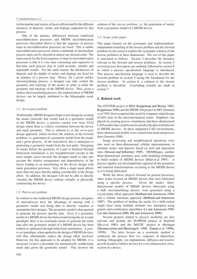
Figure 12. Generation of potential masks.
l = l + 1;o1 = P.StepsList[i];
M̃i = M̃i−1; //instantiate the current modelM̃i = Dope(M̃i, ol, unmasked); //Perform unmaskeddoping on intermediate geometric modelm̄i = GenerateMasks(); //generate a potential mask set. . . //steps similar to etching in obtaining the correct
masksM̃i = Dope(M̃i, ol, m̄i); //update the intermediategeometric model with the correct mask}
}
6.1. Generating potential mask openings
Comparing the openings on corresponding layers of geometricmodels (complete and intermediate), gives an indication of themask openings of the mask for a particular etch or doping step.However, not all the predicted mask openings need to belong tothe mask associated with the step under consideration. This isbecause multiple etches/dopings can affect one layer. Hencethey are termed as potential mask openings. This sectionoutlines how these potential mask openings are generated.Sections 6.2 and 6.3 describe how to sort out whether a maskopening can be correctly associated with a particular etch step.
Etch masks are generated by extracting the first affectedlayer of the kth etch. These layers are subtracted fromeach other to detect regions of difference in layers. Thesedifferences indicate the presence of mask openings. The maskopenings are generated by extruding and skeletonizing theintersections in layers as illustrated in figure 12 and in thefollowing equations:
m̄i = C(S(Ex(L̃ − L), y1, y2))
where
L = E(M,mf ) and L̃ = E(M̃i,mf ). (7)
The mask generation procedure for dopings is given below
M̃i = Dope(M̃i, ol, nullmask)
m̄i = C(S(Ex
(E
(M,mol
) ∩ E(M̃i,mol
), y1, y2
))).
(8)
Since the procedure for doping steps is almost similar to theetches, henceforth, only etches are discussed.
6.2. Subdivision of mask openings
A single opening in a mask (as predicted by the procedure insection 6.1) may be the result of more than one etch actingon the layer under consideration. Thus each mask openingneeds to be unambiguously subdivided into distinct maskopenings, which reflect a distinct series of etches acting onthem. The cases where this occurs are enumerated belowand illustrated in figure 13. Completely overlapping masksof two distinct etches acting on the same layer will yield asingle potential mask opening. Partially overlapping masks oftwo distinct etches acting on the same layer will yield a singlepotential mask opening. Touching masks of two distinct etchesacting on the same layer will yield a single potential maskopening. Redundant etches specified in the process sequence,e.g., specifying an etch of the same parameters two times insequence, is disallowed. In all the cases mentioned above, thepotential mask opening needs to be subdivided into more thanone distinct mask openings. Two following criteria are usedfor the subdivision.
(i) The subdivision of a mask opening based on the thicknessof the last affected layer of the etch: This criterion isillustrated by the ‘process flow 1’ shown in figure 13,where the potential mask for etch e1 is subdivided basedon the thickness of the last affected layer. If the thicknessof the last affected layer changes, it is an indication thatmore than one etch has occurred. Hence, there are asmany subdivisions in the mask as the number of differentthicknesses in the layer.
(ii) The subdivision of a mask opening based on the layerwhich the last affected layer is immediately in contactwith: This criterion is illustrated by ‘process flow 3’shown in figure 13. In this case the openings of twodifferent masks are adjacent to each other and have thesame depth in the last affected layer making it impossibleto subdivide based on thickness. Hence the layersimmediately in contact with the top surface of the lastaffected layer are checked. The subdivision is based onregions of the last affected layer in contact with a distinctupper layer. The case shown in ‘process flow 2’ is acombination of ‘process flow 1’ and ‘process flow 3’.
6.3. Validating mask openings
This step follows after the distinct potential mask openingshave been generated using the procedures outlined in theprevious sections. Each distinct mask opening has to bechecked to detect whether the current etch has affected thef th layer (first affected layer of the etch under consideration).To check whether a given mask opening affects the f thlayer, it is sufficient to check the complete geometric modelalong any given line (referred to as a check line) passinganywhere through the mask opening, e.g., line AA′ or BB′ infigure 14. Note that if the subdivision of masks was
935

V Ananthakrishnan et al
Figure 13. Subdivision of mask openings to associate an etch to a particular step.
Figure 14. Check lines to validate mask openings.
not undertaken every point in the mask opening has to bechecked using the procedure described below whereas afterthe subdivision only one point in the mask opening need bechecked. Coordinates are then given to the complete geometricmodel along the check line. The coordinates are simply the‘measured’ thicknesses of layers along the check line from topto bottom.
Figure 14 shows the coordinates along check lines AA′
and BB′. The coordinates exist in J -dimensional space �J ,where J is the maximum number of deposited layers. Since the
example illustrated in figure 3 has three deposited layers, thecoordinates in figure 14 lie in �3. Each etch and deposit is alsogiven a coordinate depending on the thickness of the depositand the depth of the etch. The coordinate of a deposit is avector with a single positive entry corresponding to the depositthickness. The coordinate of an etch is a vector with negativeentries corresponding to the etch depth in each affected layer.Coordinates of the deposits of figure 3 are listed in (27).
d1 →
00t1
d2 →
0t20
d3 →
t300
e1 →
0−t2
−fe1t1
e2 →
−t3−t2
−fe2t1
. (9)
Each coordinate of the check line is a result of a linearcombination of a sequence of deposits, and etches as shownbelow for check lines AA′ and BB′, respectively:
t30
(1 − fe1)t1
= c1
0−t2
−fe1t1
+ c2
−t3−t2
−fe2t1
+ c3
00t1
+ c4
0t20
+ c5
t300
(10a)
936

Systematic mask synthesis for surface micromachined microelectromechanical systems
00
(1 − fe2)t1
= c1
0−t2
−fe1t1
+ c2
−t3−t2
−fe2t1
+ c3
00t1
+ c4
0t20
+ c5
t300
. (10b)
At a given check line, the unknown constants ci (i = 1, . . . , 5)
can only take values of 0 or 1 because an etch/deposit either isthere or not. In particular, the constants related to deposits (i.e.ci (i = 3, . . . , 5)) are always 1 because deposits always exist.Thus to detect whether a particular etch occurred at a checkline, one needs to find the values of the constants ci (i = 1, 2)
related to the etches. For a general process with J depositsand K etches, this will yield J equations in K unknowns.The system of equations will be over-constrained, perfectlyconstrained or under-constrained depending on whether thenumber of deposits is greater than, equal to or lesser thanthe number of etches. In all the cases, there can be multiplesolutions, one solution or no solutions depending on the rankof the above linear system of equations. Another notable pointis that all the equations are independent of deposit thicknessesand only depend on the fractional depths of the etches. Theequations above simplify to the form:
[A]{c} = {b}. (11)
For check lines AA′ and BB′, respectively, equation (11) canbe obtained as 0 1
1 1fe1 fe2
{c1
c2
}=
01
fe1
and
0 1
1 1fe1 fe2
{
c1
c2
}=
01
fe2
. (12)
The general solution of the system of equations involves usinga singular value decomposition (SVD) to find the basic andfree variables (Strang 1988, Press et al 1993). If there areR free variables, there are 2R potential solutions because thevariables here can only take on the values 0 and 1. However,not all the 2R solutions need be feasible because the basicvariables may not be only 1s and 0s. Thus the system ofequations can potentially yield zero, one or multiple solutions.The situation of no solutions implies that the given devicecannot be fabricated with the specified process. Multiplesolutions imply that the given mask opening can be fabricatedby different sequences of etches. For the example shownabove the solutions are unique ((c1, c2) = (1, 0) for AA′ and(c1, c2) = (0, 1) for BB′) and correspond to the original maskopenings in figure 3.
The above solution procedure thus gives an answer as towhether the given etch ek is present or absent for a given maskopening. If the etch is present, then the mask opening can bekept, if not, the mask opening needs to be closed. If thereare multiple feasible solutions, user input is required to selecta given solution or multiple branches of solutions could bemaintained. Additionally, if the status of a prior etch has beendetermined (i.e. the corrected mask openings of a previous etchhave already been calculated and determined), there will be areduction in the number of variables. In summary, the stepsinvolved in detecting and eliminating incorrect mask openingsare
Figure 15. A difficulty of mask-dependent variable thickness inplanar and via deposits.
1. Select any check line that passes through the given maskopening.
2. Find the coordinates of the geometric model along thecheck line.
3. Find the coordinates of all the etches and deposits.4. Express the coordinates along the check line as a linear
combination of etches and deposits to get a system oflinear equations.
5. Solve the system of linear equations using SVD, whiletaking care to ensure that some variables may have beenassigned values previously.
6. If there are multiple solutions, prompt the designer todecide on whether or not the mask opening will remain.
7. Finally, retain or eliminate (i.e. close up) the potentialmask openings depending on the solution.
6.4. Remarks on the inverse problem: assumptions andrestrictions
The main assumption made in the inverse problem is that thesacrificial layers are assumed to be present (i.e. the device isnot released) in the complete geometric model of the device.This is not a serious limitation because the designer can easilyadd sacrificial layer to the part being designed. However, thisconstraint should be relaxed in future work where the designof the device is taken into account, as the sacrificial layersdo not contribute to the structural behavior of the device. Arestriction that the solution to the inverse problem presentedin this paper imposes on the process is that planar and viadeposited layers cannot be the last affected layer of any etch.This is so because, to etch the last affected layer, it is requiredthat its thickness be known consistently. In the case of planarand via deposited layers, the thickness of a layer at any pointis a variable, which depends on the surface topography of thedevice at the previous stage. For example in figure 15, it is notpossible to know the depth to which the planar or via depositedlayers can be etched without affecting the layer below it.
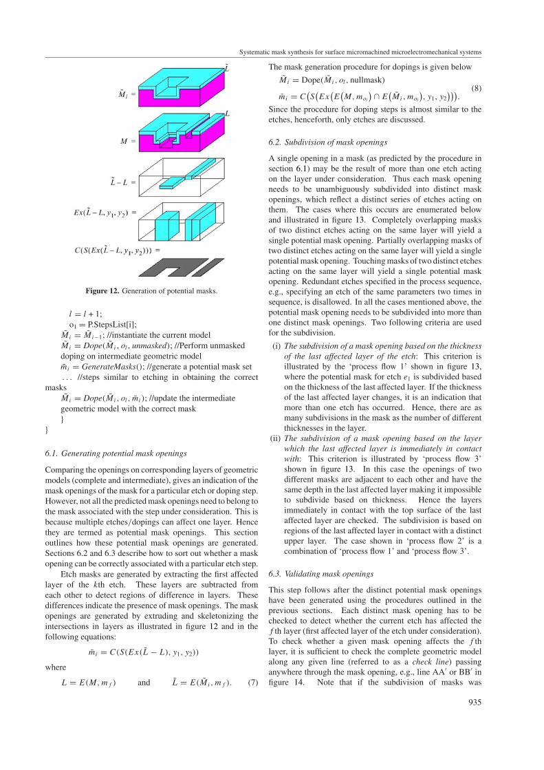
Three special cases have been identified in dealing withthe inverse problem. Consider the problem of finding thecoordinates of the checkline CC′ in figure 16(a). In this case,the thickness of the layer will be greater than the correspondingthickness of the deposit. Requiring that the coordinate (thatis greater than the thickness of the corresponding deposit) tobe equal to the thickness of the corresponding deposit yieldscorrect solutions under the assumptions stated in the previoussections.
Figure 16(b) shows another special case where anundercut etch e1 = Etch(undercut, 2, {2, 1, 0}, 0} in layer d1
937
V Ananthakrishnan et al
Figure 16. Three special cases encountered in the inverse problem. All three are resolved.
(a) (b)
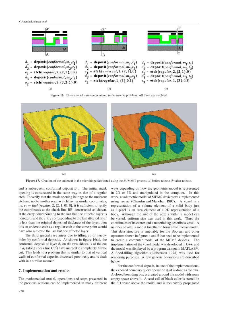
Figure 17. Creation of the undercut in the microhinge fabricated using the SUMMiT process (a) before release (b) after release.
and a subsequent conformal deposit d3. The initial maskopening is constructed in the same way as that of a regularetch. To verify that the mask opening belongs to the undercutetch and not to another regular etch having similar coordinates,i.e. e1 = Etch(regular, 2, {2, 1, 0}, 0}, it is sufficient to verifythe coordinates at the check line BB′ constructed as shown.If the entry corresponding to the last but one affected layer isnon-zero, and the entry corresponding to the last affected layeris less than the original deposited thickness of the layer, thenit is an undercut etch as a regular etch at the same point wouldhave also removed the last but one affected layer.
The third special case arises due to filling up of narrowholes by conformal deposits. As shown in figure 16(c), theconformal deposit of layer d3 on the two sidewalls of the cutin d2 (along check line CC′) have merged to completely fill thecut. This leads to a problem that is similar to that of verticalwalls of conformal deposits discussed previously and is dealtwith in a similar manner.
7. Implementation and results
The mathematical model, operations and steps presented inthe previous sections can be implemented in many different
ways depending on how the geometric model is representedin 2D or 3D and manipulated in the computer. In thiswork, a volumetric model of MEMS devices was implementedusing voxels (Chandru and Manohar 1997). A voxel is arepresentation of a volume element of a solid body justas a pixel is an area element of a 2D representation of abody. Although the size of the voxels within a model canbe varied, uniform size was used in this work. Thus, thecoordinates of its center and a material tag describe a voxel. Anumber of voxels are put together to form a volumetric model.This data structure is amenable for the Boolean and otheroperators shown in figures 4 and 5 that need to be implementedto create a computer model of the MEMS devices. Theimplementation of the voxel model was developed in C++, andthe model was displayed by a program written in MATLAB R©.A flood-filling algorithm (Lieberman 1978) was used forrendering purposes. A few generic operations are describedbelow.
For the conformal deposit, in one of the implementations,the exposed boundary query operation ∂eM is done as follows.A closed bounding box is created around the model with someempty space above it. A seed cell of black color is started inthe 3D space above the model and is recursively propagated
938

Systematic mask synthesis for surface micromachined microelectromechanical systems
(a) (b)
Figure 18. Simulation of a micromotor fabricated using the MUMPs (a) before release (b) after release.
Figure 19. A hypothetical surface-micromachined device to illustrate the potential versus corrected masks.
until no more empty cells are found. In the recursive process,whenever a colored cell is encountered, it is marked as anexposed boundary. The Minkowski operation (denoted by ⊕)is done by scanning a sphere-structuring element along theexposed boundary. A stack deposit is implemented by findingthe top-most cell height and knowing the thickness of thedeposited layer, a rectangular prism of voxels is created withappropriate material and added to the model. The via depositoperation uses the flood-fill algorithm. The isotropic etchis similar to the conformal deposit with the difference thatthe sphere of ‘empty’ material is swept across the exposedboundary. For an anisotropic vertical etch, from a given mask,
a rectangular prism of voxels of suitable size is created and issubtracted from the model.
Some of the results of forward problem are shown infigures 17 and 18. Figures 17(a) and (b) show the voxel-modelof the undercut used in the microhinge created with SUMMiTprocess. Different gray scale shades (colors) are used to showdifferent layers. The darkly shaded (blue) layer at a distanceaway from the cylinder at the center is the moving part. Ascan be seen in figure 17(b), after removing the sacrificial layer(lightly shaded (yellow) layer in figure 17(a)), the moving partcan only rotate with little clearance in the vertical and radialdirections. Additional layers are used in the SUMMiT process
939

V Ananthakrishnan et al
Figure 20. A five-layer part whose masks are to be synthesized for the process shown.
Figure 21. Two valid sets of masks synthesized for the part shownin figure 20.
to create gears with teeth at multiple levels, etc. Figure 18shows the essential parts of the electrostatic micromotor usingthe MUMPs process. In the released image (figure 18(b)), thecentral hub (pin-shaped part), the rotor with feet and the statoraround the rotor can be seen. Different shades (colors) herecorrespond to different layers (polysilicon and oxide).
Figures 19–21 show two examples of the inverse problem.Figure 19 illustrates how a potential mask is corrected andvalidated by following through with the intermediate modelas described in sections 6.1 through 6.3. Figure 20 showsa hypothetical five-layer part along with a process flow usedto create it. The application of the procedure described insection 6 results in two sets of masks (figure 21) that yield thesame 3D model of the part. Thus, this example shows thatmultiple solutions can be identified when such a situation isencountered.
8. Closure
In this paper, the geometric mask synthesis problem forsurface-micromachined devices was posed systematically andsolved mathematically using singular value decomposition ofa linear system of equations. The main contribution of thispaper is the foundation for a systematic method to perform theforward and inverse problems that facilitate the modeling andprocess planning of MEMS devices. This enables a MEMSdesigner to automatically generate masks from a geometricmodel of the MEMS device. Furthermore, it relieves theMEMS designer the necessity to constantly check if a changein the design is compatible with a process when trying toimprove the performance of a device. Future modeling workwill focus on relaxing some of these assumptions so that theinverse problem can be undertaken for a larger domain ofMEMS devices fabricated by processes other than surfacemicromachining. Finally, while the inverse problem is able tofind all solutions for mask openings, it is not able to currentlysuggest a feasible process that can fabricate the device whenno solutions are found. This is another practically usefulextension of this work.
Acknowledgments
The grant support DMI-9970021 (RS) and DMI-9970059(GKA) by National Science Foundation is gratefullyacknowledged. The authors wish to acknowledge AndrewPerrin for suggesting the flood-fill algorithm and forimplementing it as part of his NSF–REU work at the Universityof Pennsylvania. Partial support from the Iowa StateUniversity Carver Trust Grant is also gratefully acknowledgedby RS.
References
Ananthakrishnan V 2000 Part to art: The basis for a systematicgeometric design tool for surface micromachined MEMSMasters thesis University of Toledo Toledo OH USA
Chandru V and Manohar S 1997 Volume modeling for emergingmanufacturing technologies Sadhana 22 199–216
Dixit H, Kannapan S and Taylor D L 1997 3D geometric simulationof MEMS fabrication processes: A semantic approach Proc.4th ACM Symposium on Solid Modeling and Applicationspp 376–87
940

Systematic mask synthesis for surface micromachined microelectromechanical systems
Fatikow S and Rembold U 1997 Microsystem Technology andMicrorobotics (Berlin: Springer)
Hasanuzzaman M and Mastrangelo C H 1996 Process compilationof thin film microdevices IEEE Trans. Comput.-Aided Des.Integra. Circuits Syst. 15 745–64
Ho C P, Plummer J D, Hansen S E and Dutton R W 1983 VLSIprocess modeling—SUPREM III IEEE Trans. ElectronDevices 30 1438–53
Hubbard T and Antonsson E K 1994 Emergent faces in crystaletching J. Microelectromech. Syst. 3 19–28
Hubbard T and Antonsson E K 1997 Cellular automata in MEMSdesign Sensors Mater. 9 437–48
Koppelman G M 1989 OYSTER: A three-dimensional structuralsimulator for microelectromechanical design Sensors Actuators20 179–85
Koppelman G M and Wesley M A 1983 OYSTER: A study ofintegrated circuits as three-dimensional structures IBM J. Res.Dev. 27 149–63
Kumar V and Dutta D 1998 Approach to modeling andrepresentation of heterogeneous objects ASME J. Mech. Des.120 659–67
Lee C-Y and Antonsson E K 2000 Self-adapting vertices for masklayout synthesis Modeling and Simulation of MicrosystemsConference (San Diego, March 27–29)ed M Laudon andB Romanowicz pp 83–6
Li H and Antonsson E K 1998 Evolutionary techniques in MEMSsynthesis Proceedings of the ASME Design EngineeringTechnical Conferences (Atlanta, GA)
Lieberman H 1998 How to color in a coloring book SIGGRAPH 78(Atlanta GA, August) (New York: ACM) pp 111–6
Ma L and Antonsson E K 2000 Automated mask-layout and processsynthesis for MEMS Modeling and Simulation of MicrosystemsConference (San Diego, March) ed M Laudon andB Romanowicz pp 20–23
Madou M J 1997 Fundamentals of Microfabrication (Boca RatonFL: CRC Press)
Osterberg P M and Senturia S D 1995 MEMBUILDER: Anautomated solid model construction program formicromechanical structures Proc. Inter. Conf. Solid StateSensors and Actuators and Eurosensors IX vol 2 pp 21–4
Press W H, Teukolsky S A, Vetterling W T and Flannery B P 1993Numerical Recipes in C: The Art of Scientific Computing(Cambridge: Cambridge University Press)
Senturia S D, Harris R M, Johnson B P, Kim S, Nabors K,Shulman M A and White J K 1992 A computer-aided designsystem for microelectromechanical systems IEEE/ASMEJ. Microelectromech. Syst. 1 3–13
Senturia S D 1998 CAD challenges for microsensors,microactuators, and microsystems Proc. IEEE 861611–26
Smith A R 1979 Tint fill SIGGRAPH 79 (Chicago IL, August)(New York: ACM) pp 276–83
Sniegowski J J 1996 Multi-level polysilicon surfacemicromachining technology: Applications and issues Invitedpresentation at the 1996 ASME International MechanicalEngineering Congress and Exposition (Atlanta GA, Nov)
Strang G 1988 Linear Algebra and Its Applications (San Diego:Harcourt Brace Jovanovich)
Strasser E and Selberherr S 1995 Algorithms for cellular basedtopography simulation IEEE Trans. Comput.- Aided Des.Integr. Circuits Syst. 14 1104–14
Zaman M H, Carlen E T and Mastrangelo C H 1999a Automaticgeneration of thin film process flows. Part I: Basic algorithmsIEEE Trans. Semiconduct. Manuf. 12 116–28
Zaman M H, Carlen E T and Mastrangelo C H 1999b Automaticgeneration of thin film process flows. Part II: Recipegeneration, flow evaluation, and system framework IEEETrans. Semicond. Manuf. 12 129–38
941