synthesize the rtl model - carleton universityjknight/97.478/fredpetesynthch4.pdf · this step will...
TRANSCRIPT
From RTL Description to Layout
PN&JK 14 March/28/2000
4
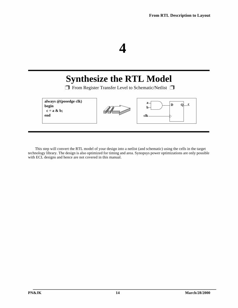
This step will convert the RTL model of your design into a netlist (and schematic) using the cells in the target technology library. The design is also optimized for timing and area. Synopsys power optimizations are only possible with ECL designs and hence are not covered in this manual.
Synthesize the RTL Model From Register Transfer Level to Schematic/Netlist
always @(posedge clk)begin c = a & b;end
ab
clk
D Q c
From RTL Description to Layout
PN&JK 15 March/28/2000
This preface is written by Fred Ma as a final touch to the document originating and developed by Peter Nyasulu and John Knight. The suggestions presented here are not necessarily the “best” way to do things. They are merely the smoothest I have found so far.
This chapter describes using a Synopsys tool to compile your Verilog description of hardware to a gate-level netlist. You can guide Synopsys by using either the menu-driven interface called the “design_analyzer”, or by enter-ing a series of command lines in a program called “dc_shell” (for Design Compiler Shell). The menus are good for exploring the command options since they are all appear in the popup windows. The dc_shell approach is more like a going through a series of calculations in matlab.
Menus and Scrip Files:
The buttons and popup menus of the Design Analyzer are helpful in the beginning but you should quickly change to using typed commands from a script file. It is much quicker since you will be running the same steps many times in the process of fine tuning the constraints for your compilation. You can use both the command lines and the menus in the Design Analyzer by poping up a dc-shell window (Setup->Command_Window). You can have the dc_shell execute entire script files of commands by using the “include” command (type “help include” in the Command Win-dow).
Along this vein, any commands issued via the GUI menus/buttons will be stored in a log file that you can edit separately, and then invoked as a script. This file is called “command.log” if the dc_shell was started up from Design Analyzer (as opposed to starting dc_shell from the UNIX prompt). You can edit this script to contain only command lines and only those you want. So you need only go through a lengthy sequence of searching for buttons once, after which you can repeat the entire sequence by invoking the script.
Getting Help:Use “help” command at dc_shell prompt.
There is an on-line help menu button in the upper right corner of the Design Analyzer GUI window.
The pdf documents are avaliable from the Design Comiler dc_shell. From the Unix prompt type-
acroread /CMC/tools/synopsys.1998.08-1/doc/online/top.pdf &
The Cadence documentation is in
/CMC/tools/cadence/tools/bin/openbook
Warnings and Errors:
Synthesis will generate lots of information. My suggestion is that you search for warnings or errors by scanning the output, which will be copied to “view_command.log” if dc_shell was started from Design Analyzer. You could even open the file and do a case-insensitive search for “warning” and “error”. Just don’t change the file and save it again if the dc_shell is still active.
Editing on a PCFiles that have been imported from a PC to unix may have ^M^M at the end of each line. Synopsys blows up on this.
Delete Garbage Before a Rerun: If you want to redo in your synthesis steps, exit the compiling session. Otherwise, Synopsys happily run using conditions from the old session. In addition to exiting from dc_shell or Design Analyzer, I have found my results much more repeatable if I erase all files created during the compilation process. For example, if your module was named “design”, then run the following commands from the UNIX prompt (including the capitalization of “design”):
rm filenames.log
4.1 Preface: Things to keep in mind
From RTL Description to Layout
PN&JK 16 March/28/2000
rm DESIGN.mra rm design%verilog.syn
rm design%verilog__verilog.syn rm design.db # Your design in Synopsys internal format rm design.vdb #Test vectors rm designGateLevel.v rm command.log rm view_command.log rm wcells_testsim.db rm design_schk.v rm design_0.v rm verilog.key rm verilog.log rm design_0.WGL rm design_schk.WGL
For a script file use rm -rf to remove recursively inside Work. Use $1 to pass arguments
Of course, this is too much to type in all the time, so you can put these commands into a file cleanup, after which you can run it by typing ./cleanup. But first you have to turn it into a runnable file by typing
chmod u+x cleanup rehash
Using Verilog XLSet your path for Cadence. path=($path /CMC/tools/cadence/tools/dfII/local/bin)
Fix Your Test Bench for Scan Testing:By the end of this synthesis flow your design will have extra circuitry for scan testing, etc. This means it will
have extra ports for scan-in, scan-out, and scan-enable pins. Furthermore, any arrayed signals will not be arrayed in the synthesized netlist; instead, the array elements will be listed as separate signals.
You will need to add these changes to your testbench. In addition you must also tell verilog where to get the models for the synthesized circuit cells that your design mapped to. Do this by adding these lines to your test bench:
`define WCELLS dir=/CMC/kits/cmosp35/models/verilog/nwb `define WCELLUDP dir=/CMC/kits/cmosp35/models/verilog/udp `uselib `WCELLS `WCELLUDP
Also be sure the testbench is the first file in your verilog command:
verilog testbench.v topmoduledb.v
That’s it for now. Good luck!
From RTL Description to Layout
PN&JK 17 March/28/2000
Synopsys Design Analyzer provides a graphical (menu-driven and command-line) interface to the Synopsys tools you will be using during synthesis (VHDL Compiler, HDL Compiler, Design Compiler, Test Compiler, Design Time).
4.2 Start the Synopsys Design Analyzer
• To start the Design Analyzer, type the following at the Unix prompt (The & starts the Design Analyzer in background so that you can use the Unix window for other commands):
design_analyzer &↵
• Optionally, you can use the Design Compiler (dc) shell and run the synthesis using dc shell commands only. Since the dc shell is a text-based window, you will not be able to see the schematic. It is therefore not advisable to use the dc shell alone unless you are very experienced. You will be able to run a combination of scrip com-mands and menu commands by using the command windopw inside the design anaylzer.
To start the dc shell, type the following at the Unix prompt:
dc_shell↵
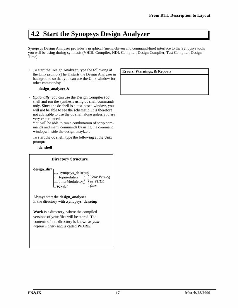
Directory Structure
design_dir/.synopsys_dc.setuptopmodule.votherModules.v
Work/
Always start the design_analyserin the directory with .synopsys_dc.setup
Your Verilogor VHDLfiles
Work is a directory, where the compiled
default library and is called WORK.
versions of your files will be stored. The contents of this directory is known as your
Errors, Warnings, & Reports
From RTL Description to Layout
PN&JK 18 March/28/2000
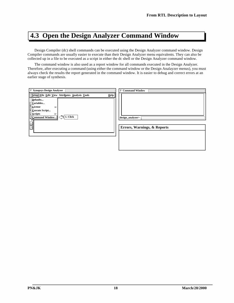
Design Compiler (dc) shell commands can be executed using the Design Analyzer command window. Design Compiler commands are usually easier to execute than their Design Analyzer menu equivalents. They can also be collected up in a file to be executed as a script in either the dc shell or the Design Analyzer command window.
The command window is also used as a report window for all commands executed in the Design Analyzer. Therefore, after executing a command (using either the command window or the Design Analayzer menus), you must always check the results the report generated in the command window. It is easier to debug and correct errors at an earlier stage of synthesis.
4.3 Open the Design Analyzer Command Window
P Synopsys Design Analyzer
È
È
T
P Command Window
design_analyzer>
Errors, Warnings, & Reports
Defaults...Variables...License Execute Script...Scripts Command Window...
∆
∆
File Edit View Attributes Analysis Tools Help Setup
1. Click
From RTL Description to Layout
PN&JK 19 March/28/2000
topmod
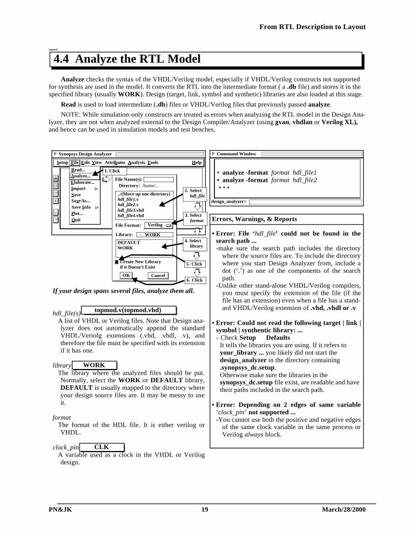
Analyze checks the syntax of the VHDL/Verilog model, especially if VHDL/Verilog constructs not supported for synthesis are used in the model. It converts the RTL into the intermediate format ( a .db file) and stores it in the specified library (usually WORK). Design (target, link, symbol and synthetic) libraries are also loaded at this stage.
Read is used to load intermediate (.db) files or VHDL/Verilog files that previously passed analyze.
NOTE: While simulation-only constructs are treated as errors when analyzing the RTL model in the Design Ana-lyzer, they are not when analyzed external to the Design Compiler/Analyzer (using gvan, vhdlan or Verilog XL), and hence can be used in simulation models and test benches.
4.4 Analyze the RTL Model
• Error: File ‘hdl_file’ could not be found in thesearch path ...-make sure the search path includes the directory
where the source files are. To include the directorywhere you start Design Analyzer from, include adot (‘.’) as one of the components of the searchpath.
-Unlike other stand-alone VHDL/Verilog compilers,you must specify the extension of the file (if thefile has an extension) even when a file has a stand-ard VHDL/Verilog extension of .vhd, .vhdl or .v
• Error: Could not read the following target | link |symbol | synthentic library: ...- Check Setup ⇒ Defaults
It tells the libraries you are using. If it refers to your_library ... you likely did not start the design_analyzer in the directory containing .synopsys_dc.setup.Otherwise make sure the libraries in the synopsys_dc.setup file exist, are readable and have their paths included in the search path.
• Error: Depending on 2 edges of same variable‘clock_pin’ not supported ...-You cannot use both the positive and negative edges
of the same clock variable in the same process orVerilog always block.
P Synopsys Design Analyzer
È
È
T
P Command Window
• analyze -format format hdl_file1↵• analyze -format format hdl_file2↵ • • •
design_analyzer>
If your design spans several files, analyze them all.
hdl_file(s)A list of VHDL or Verilog files. Note that Design ana-lyzer does not automatically append the standardVHDL/Veriolg extensions (.vhd, .vhdl, .v), andtherefore the file must be specified with its extensionif it has one.
libraryThe library where the analyzed files should be put.Normally, select the WORK or DEFAULT library,DEFAULT is usually mapped to the directory whereyour design source files are. It may be messy to useit.
formatThe format of the HDL file. It is either verilog orVHDL.
clock_pinA variable used as a clock in the VHDL or Verilogdesign.
topmod.v(topmod.vhd)
WORK
CLK
Errors, Warnings, & Reports
File Name(s):Directory: /home/...
Create New Libraryif it Doesn’t Exist
File Format:
../(Move up one directory)hdl_file1.vhdl_file2.vhdl_file3.vhdhdl_file4.vhd
Verilog
Library:
DEFAULTWORK
OK Cancel
2. Selecthdl_file
3. Selectformat
4. Selectlibrary
5. Click
File Edit View Attributes Analysis Tools Help Setup
Read...Analyze...Elaborate...
SaveSave As... Save Info ∆
Plot... Quit
Import ∆
1. Click
6. Click
WORK
From RTL Description to Layout
PN&JK 20 March/28/2000
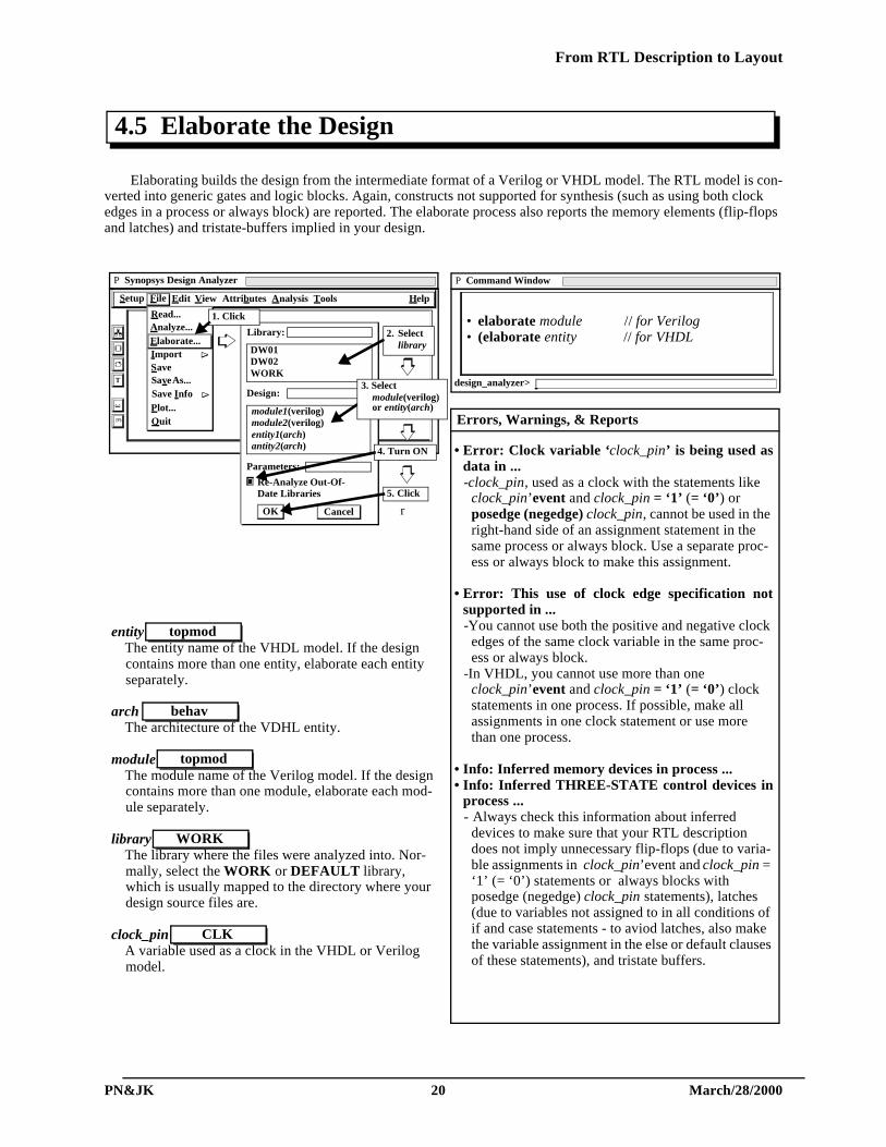
Elaborating builds the design from the intermediate format of a Verilog or VHDL model. The RTL model is con-verted into generic gates and logic blocks. Again, constructs not supported for synthesis (such as using both clock edges in a process or always block) are reported. The elaborate process also reports the memory elements (flip-flops and latches) and tristate-buffers implied in your design.
4.5 Elaborate the Design
• Error: Clock variable ‘clock_pin’ is being used asdata in ...-clock_pin, used as a clock with the statements like
clock_pin’event and clock_pin = ‘1’ (= ‘0’) or posedge (negedge) clock_pin, cannot be used in the right-hand side of an assignment statement in the same process or always block. Use a separate proc-ess or always block to make this assignment.
• Error: This use of clock edge specification notsupported in ...-You cannot use both the positive and negative clock
edges of the same clock variable in the same proc-ess or always block.
-In VHDL, you cannot use more than one clock_pin’event and clock_pin = ‘1’ (= ‘0’) clock statements in one process. If possible, make all assignments in one clock statement or use more than one process.
• Info: Inferred memory devices in process ...• Info: Inferred THREE-STATE control devices in
process ...- Always check this information about inferred
devices to make sure that your RTL description does not imply unnecessary flip-flops (due to varia-ble assignments in clock_pin’event and clock_pin = ‘1’ (= ‘0’) statements or always blocks with posedge (negedge) clock_pin statements), latches (due to variables not assigned to in all conditions of if and case statements - to aviod latches, also make the variable assignment in the else or default clauses of these statements), and tristate buffers.
P Synopsys Design Analyzer
È
È
T
P Command Window
• elaborate module↵ // for Verilog• (elaborate entity↵) // for VHDL
design_analyzer>
entityThe entity name of the VHDL model. If the design contains more than one entity, elaborate each entity separately.
archThe architecture of the VDHL entity.
moduleThe module name of the Verilog model. If the design contains more than one module, elaborate each mod-ule separately.
libraryThe library where the files were analyzed into. Nor-mally, select the WORK or DEFAULT library, which is usually mapped to the directory where your design source files are.
clock_pinA variable used as a clock in the VHDL or Verilog model.
topmod
behav
topmod
WORK
CLK
Errors, Warnings, & Reports
Library:
Re-Analyze Out-Of-Date Libraries
module1(verilog)module2(verilog)entity1(arch)antity2(arch)
Parameters:
DW01DW02WORK
OK Cancel
Design:
2. Selectlibrary
3. Selectmodule(verilog)or entity(arch)
4. Turn ON
5. Click
File Edit View Attributes Analysis Tools Help Setup
Read...Analyze...Elaborate...
SaveSave As... Save Info ∆
Plot... Quit
Import ∆
r
1. Click
From RTL Description to Layout
PN&JK 21 March/28/2000
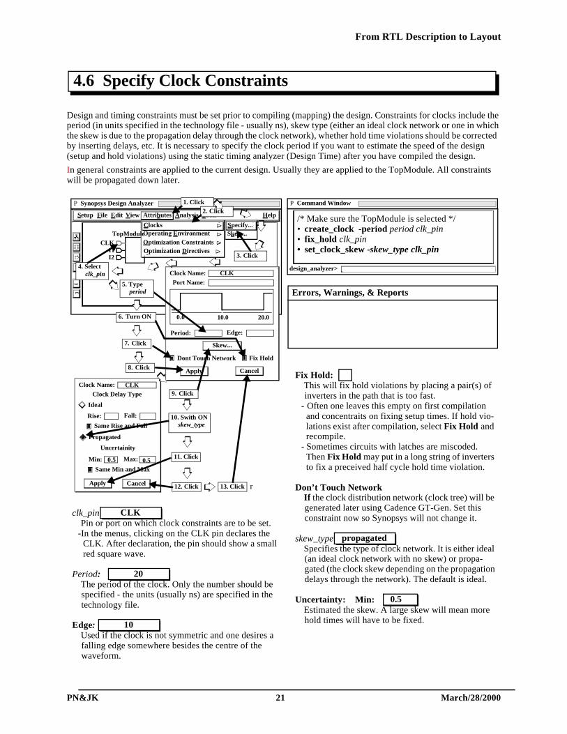
Design and timing constraints must be set prior to compiling (mapping) the design. Constraints for clocks include the period (in units specified in the technology file - usually ns), skew type (either an ideal clock network or one in which the skew is due to the propagation delay through the clock network), whether hold time violations should be corrected by inserting delays, etc. It is necessary to specify the clock period if you want to estimate the speed of the design (setup and hold violations) using the static timing analyzer (Design Time) after you have compiled the design.
In general constraints are applied to the current design. Usually they are applied to the TopModule. All constraints will be propagated down later.
4.6 Specify Clock Constraints
P Synopsys Design Analyzer
È
È
T
P Command Window
/* Make sure the TopModule is selected */• create_clock -period period clk_pin↵• fix_hold clk_pin↵ • set_clock_skew -skew_type clk_pin↵
design_analyzer>
clk_pin Pin or port on which clock constraints are to be set.
-In the menus, clicking on the CLK pin declares the CLK. After declaration, the pin should show a small red square wave.
Period: The period of the clock. Only the number should be specified - the units (usually ns) are specified in the technology file.
Edge: Used if the clock is not symmetric and one desires a falling edge somewhere besides the centre of the waveform.
CLK
20
10
Errors, Warnings, & Reports
Clock Name:
Dont Touch Network
0.0
Skew...
Period:
Cancel
Port Name:
Fix Hold
Apply
10.0 20.0
Edge:
Clock Name:
Rise:
Cancel
Clock Delay Type
Apply
Fall:
Same Rise and Fall
Ideal
Propagated
Min:
Uncertainity
Max:
Same Min and Max
6. Turn ON
8. Click
7. Click
10. Swith ONskew_type
11. Click
12. Click 13. Click
File Edit View Attributes Analysis Tools Help Setup
r
4. Selectclk_pin
5. Typeperiod
CLKI1I2
O1O2
Specify...Skew...
ClocksOperating EnvironmentOptimization ConstraintsOptimization Directives
∆
∆
∆
∆
3. Click
1. Click2. Click
Fix Hold: This will fix hold violations by placing a pair(s) of inverters in the path that is too fast.
- Often one leaves this empty on first compilation and concentraits on fixing setup times. If hold vio-lations exist after compilation, select Fix Hold and recompile.
- Sometimes circuits with latches are miscoded. Then Fix Hold may put in a long string of inverters to fix a preceived half cycle hold time violation.
Don’t Touch NetworkIf the clock distribution network (clock tree) will be generated later using Cadence GT-Gen. Set this constraint now so Synopsys will not change it.
skew_typeSpecifies the type of clock network. It is either ideal (an ideal clock network with no skew) or propa-gated (the clock skew depending on the propagation delays through the network). The default is ideal.
Uncertainty: Min:Estimated the skew. A large skew will mean more hold times will have to be fixed.
propagated
0.5
9. Click
CLK
0.5
TopModule
CLK
0.5

From RTL Description to Layout
PN&JK 22 March/28/2000
Synopsys Test Compiler can automatically insert boundary scan and/or scan test circuitry into your design. The two scan test methodologies are full scan test and partial scan test. In full scan test, all clocked latches and flip flops are replaced by their scannable equivalents In partial scan tests, a constraint-driven scan selection algorithm is used to select certain flip flops to makescannable. Partial scan therefore has less speed and area costs than full scan, but has a lower fault coverage than the later.
In the Multiplexed flip-flop style of scan test design the input to a flip flop is multiplexed between the normal circuit data and the scan test. The other scan styles are described briefly in Appendix A.1.
If scan test is to be done, we warn Synopsys here so the synthesizer will use scanable flip-flops and/or muxs during synthesis. This may avoid getting timing violations when the actual test circuitry is inserted later.
4.7 Set Scan Test Style Constraints
P Synopsys Design Analyzer
È
È
T
P Command Window
• set_scan_style scan_style↵
design_analyzer>
scan_styleDefines the scan-test implementation. It is either multiplexed_flip_flop, lssd, aux_clock_lssd, clocked_scan, combinational or none. See Appen-dix A.1 for details.
multiplexed_flip_flop
Errors, Warnings, & Reports
Design...Input Port...Output Port...Cell...Pin... Net...Timing Paths...
1. Selectscan_style
2. Click
3. Click
File Edit View Attributes Analysis Tools Help Setup
ClocksOperating EnvironmentOptimization ConstraintsOptimization Directives
∆
∆
∆
∆
Design Name:
Flatten Effort:
CancelApply
Structured Logic
Low
Boundary Optimization
Port is Pad:
Ungroup
Disable Wired Logic (E
Single Output
Flatten Minimize: Flatten Phase:
Don’t ApplyMedium Multiple Output Apply StrategyHigh None
Flatten Logic
Don’t Touch
Test Scan Style: Multiplexed Flip Flop
Design Pad Attributes...
Apply Timing Driven Structuring
Apply Boolean Optimization
Sequential Elements: Latch...Flip Flop...
r
From RTL Description to Layout
PN&JK 23 March/28/2000
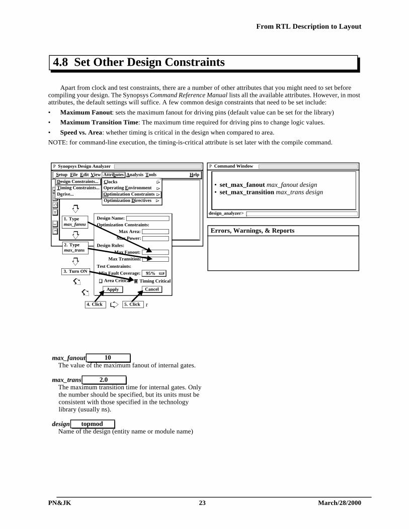
Apart from clock and test constraints, there are a number of other attributes that you might need to set before compiling your design. The Synopsys Command Reference Manual lists all the available attributes. However, in most attributes, the default settings will suffice. A few common design constraints that need to be set include:
• Maximum Fanout: sets the maximum fanout for driving pins (default value can be set for the library)
• Maximum Transition Time: The maximum time required for driving pins to change logic values.
• Speed vs. Area: whether timing is critical in the design when compared to area.
NOTE: for command-line execution, the timing-is-critical attribute is set later with the compile command.
4.8 Set Other Design Constraints
P Synopsys Design Analyzer
È
È
T
P Command Window
• set_max_fanout max_fanout design↵• set_max_transition max_trans design↵
design_analyzer>
max_fanoutThe value of the maximum fanout of internal gates.
max_transThe maximum transition time for internal gates. Only the number should be specified, but its units must be consistent with those specified in the technology library (usually ns).
designName of the design (entity name or module name)
10
2.0
topmod
Errors, Warnings, & Reports
Design Name:
Max Area:
CancelApply
Max Power:
Optimization Constraints:
Area Critical Timing Critical
Test Constraints:
Min Fault Coverage: 95%
Max Fanout:
Max Transition:
Design Rules:
1. Typemax_fanou
4. Click 5. Click
2. Typemax_trans
3. Turn ON
r
File Edit View Attributes Analysis Tools Help Setup
ClocksOperating EnvironmentOptimization ConstraintsOptimization Directives
∆
∆
∆
∆ Derive...
Design Constraints...Timing Constraints...
From RTL Description to Layout
PN&JK 24 March/28/2000
Synopsys may rename vectors as individual bits. To avoid problems wih this and other port/net related problems, ask Synopsys to fix them. This must be done in the dc_shell
You should also propagate all the constraints on the top module to the lower level modules. Again this is done in the dc_shell using characterize.
Then save the constrained module under a new name.This makes it easy to come back to this point.
4.9 Set Constraints in DC_Shell , Propagate and Save
P Synopsys Design Analyzer
È
È
T
P Command Window
• set_fix_multiple_port_nets -all↵• characterize other modinst↵
/* To save in the command window use */• write -format db -hierarchy
-output topmod_constrained.db
design_analyzer>
other_modinst
Lower level modules instances to which the con-straints should be propagated. After characterization you should see the red square wave on the clock pin of the lower level module.
- More than one instances should be in a list as illus-trated.
File_name We suggest you save your design with the sufix con-strained.db. This allows the file to be easily found and loaded for restarting from this point.
File_format The db format is Synopses’ own internal file format. Use it if the file is not used outside Synopsys.
{ modinst2, modinst2/submodinst5, modinst3, modinst3/submodinst6 }
topmod_constrained.db
db
Errors, Warnings, & Reports
File Edit View Attributes Analysis Tools Help Setup
Read...Analyze...Elaborate...
SaveSave As... Save Info ∆
Plot... Quit
Import ∆
4. Click
CLKI1I2
O1O2
TopModule
3. SelectTopModule
1. Typecommand
2. Type command
File Name:Directory: /home/...
Save All Designsin Hierarchy
File Format:
../(Move up one directory)file1file2file3file4
DB
OK Cancel
8. Click
5. Typefile_name
6. Selectfile_format
7. Turn ON
From RTL Description to Layout
PN&JK 25 March/28/2000
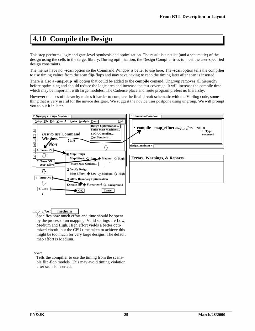
This step performs logic and gate-level synthesis and optimization. The result is a netlist (and a schematic) of the design using the cells in the target library. During optimization, the Design Compiler tries to meet the user-specified design constraints.
The menus have no -scan option so the Command Window is better to use here. The -scan option tells the compilier to use timing values from the scan flip-flops and may save having to redo the timing later after scan is inserted.
There is also a -ungroup_all option that could be added to the compile comand. Ungroup removes all hierarchy before optimizing and should reduce the logic area and increase the test coverage. It will increase the compile time which may be important with large modules. The Cadence place and route program prefers no hierarchy.
However the loss of hierarchy makes it harder to compare the final circuit schematic with the Verilog code, some-thing that is very useful for the novice designer. We suggest the novice user postpone using ungroup. We will prompt you to put it in later.
4.10 Compile the Design
P Synopsys Design Analyzer
È
È
T
P Command Window
• compile -map_effort map_effort -scan↵
design_analyzer>
map_effortSpecifies how much effort and time should be spent by the processor on mapping. Valid settings are Low, Medium and High. High effort yields a better opti-mized circuit, but the CPU time taken to achieve this might be too much for very large designs. The default map effort is Medium.
-scanTells the compilier to use the timing from the scana-ble flip-flop models. This may avoid timing violation after scan is inserted.
medium
Errors, Warnings, & Reports
Design Optimization...Finite State Machines...FPGA Compiler...
Map Effort:
Cancel
Map Design
Low Medium High
Allow Boundary Optimization
More Map Options...
Map Effort:
Verify Design
Low Medium High
Execute in: Foreground Background
OK4. Click
2. Turn ONmap_effort
1. Turn ON
r
3. Turn ON
File Edit View Attributes Analysis Tools Help Setup
Test Synthesis...
1. TypecommandBest to use Command
Window. Non
Oui
From RTL Description to Layout
PN&JK 26 March/28/2000
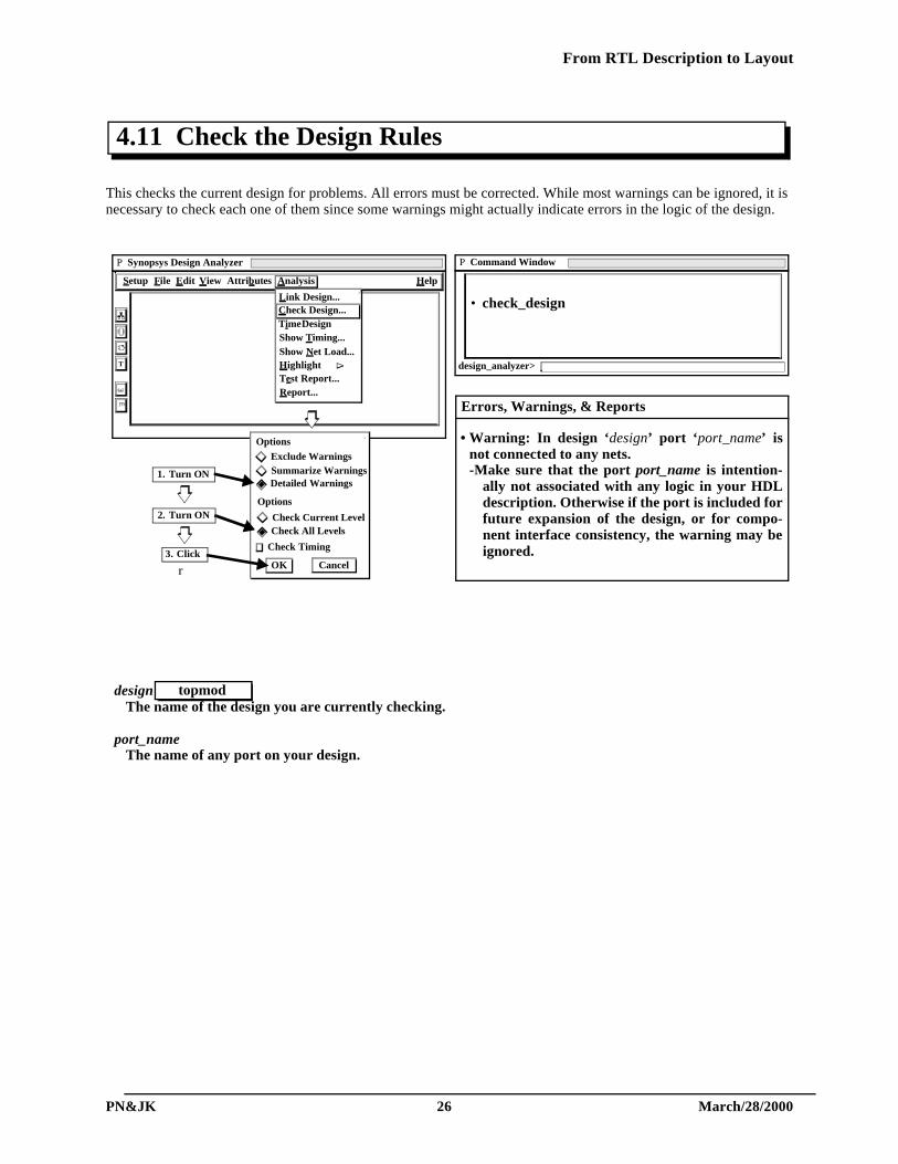
This checks the current design for problems. All errors must be corrected. While most warnings can be ignored, it is necessary to check each one of them since some warnings might actually indicate errors in the logic of the design.
4.11 Check the Design Rules
• Warning: In design ‘design’ port ‘port_name’ isnot connected to any nets.-Make sure that the port port_name is intention-
ally not associated with any logic in your HDLdescription. Otherwise if the port is included forfuture expansion of the design, or for compo-nent interface consistency, the warning may beignored.
P Synopsys Design Analyzer
È
È
T
P Command Window
• check_design↵
design_analyzer>
designThe name of the design you are currently checking.
port_nameThe name of any port on your design.
topmod
Errors, Warnings, & Reports
OK
Check Timing
Options
Detailed Warnings
Exclude WarningsSummarize Warnings
Options
Check All LevelsCheck Current Level
Cancel3. Click
r
2. Turn ON
1. Turn ON
File Edit View Attributes Analysis Help Setup
Link Design...Check Design...Time Design Show Timing...
Highlight Show Net Load...
∆
Test Report...Report...
From RTL Description to Layout
PN&JK 27 March/28/2000
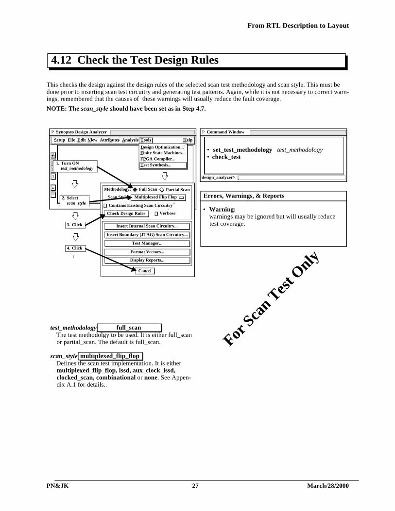
This checks the design against the design rules of the selected scan test methodology and scan style. This must be done prior to inserting scan test circuitry and generating test patterns. Again, while it is not necessary to correct warn-ings, remembered that the causes of these warnings will usually reduce the fault coverage.
NOTE: The scan_style should have been set as in Step 4.7.
4.12 Check the Test Design Rules
P Synopsys Design Analyzer
È
È
T
P Command Window
• set_test_methodology test_methodology• check_test↵
design_analyzer>
test_methodologyThe test methodolgy to be used. It is either full_scan or partial_scan. The default is full_scan.
scan_styleDefines the scan test implementation. It is either multiplexed_flip_flop, lssd, aux_clock_lssd, clocked_scan, combinational or none. See Appen-dix A.1 for details..
full_scan
multiplexed_flip_flop
• Warning:warnings may be ignored but will usually reduce test coverage.
Errors, Warnings, & Reports
Cancel
VerboseCheck Design Rules
Contains Existing Scan Circuitry
Methodology: Full Scan Partial Scan
Scan Style: Multiplexed Flip Flop
Insert Internal Scan Circuitry...
Insert Boundary (JTAG) Scan Circuitry...
Test Manager...
Format Vectors...
Display Reports...
4. Click
1. Turn ONtest_methodology
r
2. Selectscan_style
3. Click
File Edit View Attributes Analysis Tools Help Setup
Design Optimization...Finite State Machines...FPGA Compiler...Test Synthesis...
For Sca
n Tes
t Only
From RTL Description to Layout
PN&JK 28 March/28/2000
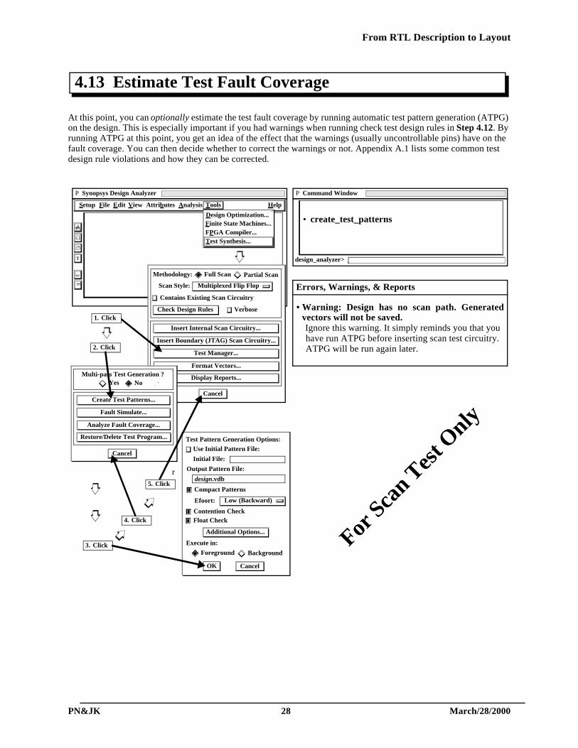
At this point, you can optionally estimate the test fault coverage by running automatic test pattern generation (ATPG) on the design. This is especially important if you had warnings when running check test design rules in Step 4.12. By running ATPG at this point, you get an idea of the effect that the warnings (usually uncontrollable pins) have on the fault coverage. You can then decide whether to correct the warnings or not. Appendix A.1 lists some common test design rule violations and how they can be corrected.
4.13 Estimate Test Fault Coverage
• Warning: Design has no scan path. Generatedvectors will not be saved.Ignore this warning. It simply reminds you that you have run ATPG before inserting scan test circuitry. ATPG will be run again later.
P Synopsys Design Analyzer
È
È
T
P Command Window
• create_test_patterns↵
design_analyzer>
Errors, Warnings, & Reports
Cancel
VerboseCheck Design Rules
Contains Existing Scan Circuitry
Methodology: Full Scan Partial Scan
Scan Style: Multiplexed Flip Flop
Insert Internal Scan Circuitry...
Insert Boundary (JTAG) Scan Circuitry...
Test Manager...
Format Vectors...
Display Reports...
5. Click
r
1. Click
4. Click
File Edit View Attributes Analysis Tools Help Setup
Design Optimization...Finite State Machines...FPGA Compiler...Test Synthesis...
Cancel
Create Test Patterns...
Fault Simulate...
Analyze Fault Coverage...
Restore/Delete Test Program...
Multi-pass Test Generation ?Yes No
Cancel
Compact Patterns
Additional Options...
Execute in:
Foreground Background
OK
Test Pattern Generation Options:
Use Initial Pattern File:
Initial File:
Output Pattern File:
design.vdb
Contention CheckFloat Check
Efoort: Low (Backward)
2. Click
3. Click For Sca
n Tes
t Only
From RTL Description to Layout
PN&JK 29 March/28/2000
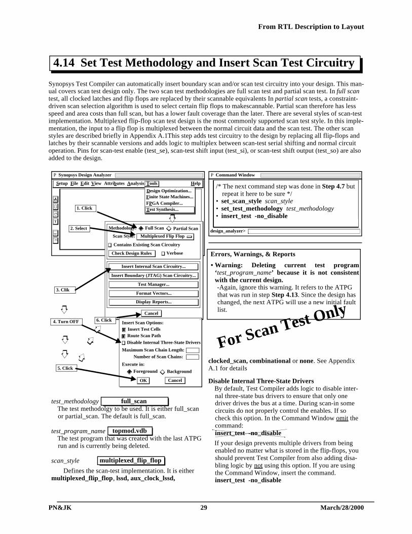
Synopsys Test Compiler can automatically insert boundary scan and/or scan test circuitry into your design. This man-ual covers scan test design only. The two scan test methodologies are full scan test and partial scan test. In full scan test, all clocked latches and flip flops are replaced by their scannable equivalents In partial scan tests, a constraint-driven scan selection algorithm is used to select certain flip flops to makescannable. Partial scan therefore has less speed and area costs than full scan, but has a lower fault coverage than the later. There are several styles of scan-test implementation. Multiplexed flip-flop scan test design is the most commonly supported scan test style. In this imple-mentation, the input to a flip flop is multiplexed between the normal circuit data and the scan test. The other scan styles are described briefly in Appendix A.1This step adds test circuitry to the design by replacing all flip-flops and latches by their scannable versions and adds logic to multiplex between scan-test serial shifting and normal circuit operation. Pins for scan-test enable (test_se), scan-test shift input (test_si), or scan-test shift output (test_so) are also added to the design.
4.14 Set Test Methodology and Insert Scan Test Circuitry
• Warning: Deleting current test program‘test_program_name’ because it is not consistentwith the current design.-Again, ignore this warning. It refers to the ATPG that was run in step Step 4.13. Since the design has changed, the next ATPG will use a new initial fault list.
P Synopsys Design Analyzer
È
È
T
P Command Window
/* The next command step was done in Step 4.7 but repeat it here to be sure */
• set_scan_style scan_style↵ • set_test_methodology test_methodology↵• insert_test -no_disable↵
design_analyzer>
test_methodology The test methodolgy to be used. It is either full_scan or partial_scan. The default is full_scan.
test_program_name The test program that was created with the last ATPG run and is currently being deleted.
scan_style
Defines the scan-test implementation. It is either multiplexed_flip_flop, lssd, aux_clock_lssd,
full_scan
topmod.vdb
multiplexed_flip_flop
Errors, Warnings, & Reports
Cancel
VerboseCheck Design Rules
Contains Existing Scan Circuitry
Methodology: Full Scan Partial Scan
Scan Style: Multiplexed Flip Flop
Insert Internal Scan Circuitry...
Insert Boundary (JTAG) Scan Circuitry...
Test Manager...
Format Vectors...
Display Reports...
Insert Scan Options:
Cancel
Disable Internal Three-State Drivers
Insert Test Cells
Maximum Scan Chain Length:
Number of Scan Chains:
Route Scan Path
Execute in:
Foreground Background
OK
5. Click
4. Turn OFF
3. Clik
6. Click
File Edit View Attributes Analysis Tools Help Setup
Design Optimization...Finite State Machines...FPGA Compiler...Test Synthesis...
For Scan Test Only
1. Click
2. Select
clocked_scan, combinational or none. See Appendix A.1 for details
Disable Internal Three-State DriversBy default, Test Compiler adds logic to disable inter-nal three-state bus drivers to ensure that only one driver drives the bus at a time. During scan-in some circuits do not properly control the enables. If so check this option. In the Command Window omit the command:insert_test -no_disable
If your design prevents multiple drivers from being enabled no matter what is stored in the flip-flops, you should prevent Test Compiler from also adding disa-bling logic by not using this option. If you are using the Command Window, insert the command. insert_test -no_disable
From RTL Description to Layout
PN&JK 30 March/28/2000
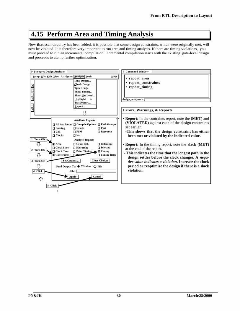
Now that scan circuitry has been added, it is possible that some design constraints, which were originally met, will now be violated. It is therefore very important to run area and timing analysis. If there are timing violations, you must proceed to run an incremental compilation. Incremental compilation starts with the existing gate-level design and proceeds to atemp further optimization.
4.15 Perform Area and Timing Analysis
• Report: In the contraints report, note the (MET) and(VIOLATED) against each of the design constraintsset earlier.-This shows that the design constraint has either
been met or violated by the indicated value.
• Report: In the timing report, note the slack (MET)at the end of the report.
- This indicates the time that the longest path in thedesign settles before the clock changes. A nega-tive value indicates a violation. Increase the clockperiod or reoptimize the design if there is a slackviolation.
P Synopsys Design Analyzer
È
È
T
P Command Window
• report_area↵• report_constraints↵• report_timing↵
design_analyzer>
Errors, Warnings, & Reports
Attribute Reports
CancelApply
All Attributes Compile Options
Clear ChoicesSet Options...
Path GroupsBussing Design PortCell FSM ResourceClocks Net
Analysis Reports
Area Cross Ref. ReferenceClock Skew Hierarchy SelectedClock Tree Point Timing TimingConstraints Power Timing Requ
Send Output To: Window File
File:
5. Click
r
3. Turn ON
2. Turn ON
1. Turn ON
4. Click
File Edit View Attributes Analysis Tools Help Setup
Link Design...Check Design...Time Design Show Timing...
Highlight Show Net Load...
∆
Test Report...Report...
From RTL Description to Layout
PN&JK 31 March/28/2000
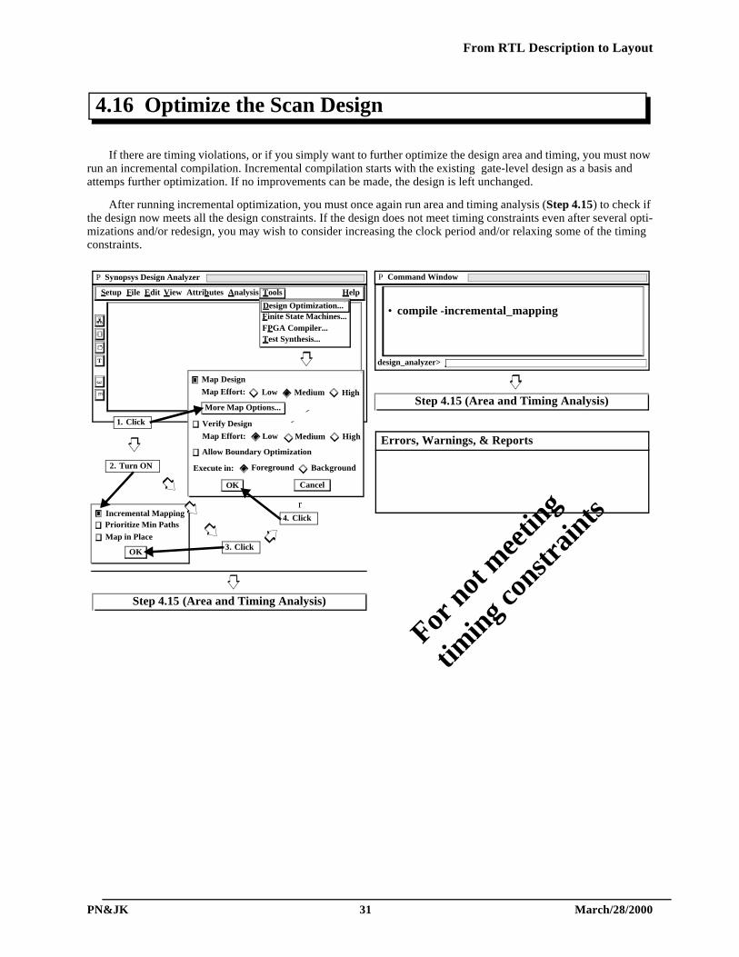
If there are timing violations, or if you simply want to further optimize the design area and timing, you must now run an incremental compilation. Incremental compilation starts with the existing gate-level design as a basis and attemps further optimization. If no improvements can be made, the design is left unchanged.
After running incremental optimization, you must once again run area and timing analysis (Step 4.15) to check if the design now meets all the design constraints. If the design does not meet timing constraints even after several opti-mizations and/or redesign, you may wish to consider increasing the clock period and/or relaxing some of the timing constraints.
4.16 Optimize the Scan Design
P Synopsys Design Analyzer
È
È
T
P Command Window
• compile -incremental_mapping↵
design_analyzer>
Errors, Warnings, & Reports
Map Effort:
Cancel
Map Design
Low Medium High
Allow Boundary Optimization
More Map Options...
Map Effort:
Verify Design
Low Medium High
Execute in: Foreground Background
OK
Incremental Mapping
OK
Prioritize Min Paths
Map in Place
r
3. Click
4. Click
1. Click
2. Turn ON
File Edit View Attributes Analysis Tools Help Setup
Design Optimization...Finite State Machines...FPGA Compiler...Test Synthesis...
Step 4.15 (Area and Timing Analysis)
Step 4.15 (Area and Timing Analysis)
For not
mee
ting
timin
g con
strain
ts
From RTL Description to Layout
PN&JK 32 March/28/2000
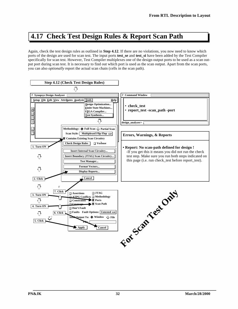
Again, check the test design rules as outlined in Step 4.12. If there are no violations, you now need to know which ports of the design are used for scan test. The input ports test_se and test_si have been added by the Test Compiler specifically for scan test. However, Test Compiler multiplexes one of the design output ports to be used as a scan out-put port during scan test. It is necessary to find out which port is used as the scan output. Apart from the scan ports, you can also optionally report the actual scan chain (cells in the scan path).
4.17 Check Test Design Rules & Report Scan Path
P Synopsys Design Analyzer
È
È
T
P Command Window
• check_test↵• report_test -scan_path -port↵
design_analyzer>
• Report: No scan-path defined for design !-If you get this it means you did not run the check test step. Make sure you run both steps indicated on this page (i.e. run check_test before report_test).
Errors, Warnings, & Reports
Cancel
VerboseCheck Design Rules
Contains Existing Scan Circuitry
Methodology: Full Scan Partial Scan
Scan Style: Multiplexed Flip Flop
Insert Internal Scan Circuitry...
Insert Boundary (JTAG) Scan Circuitry...
Test Manager...
Format Vectors...
Display Reports...
2. Click
1. Turn ON
CancelApply
Assertions JTAG
ATPG Conflicts MethodologyConstraints Ports
Coverage Scan Path
Send Output To: Window File
File:
Don’t Fault
Faults Fault Options: Untested
3. Turn ON
4. Turn ON
5. Click
6. Click
r7. Click
File Edit View Attributes Analysis Tools Help Setup
Design Optimization...Finite State Machines...FPGA Compiler...Test Synthesis...
Step 4.12 (Check Test Design Rules)
For Sca
n Tes
t Only
From RTL Description to Layout
PN&JK 33 March/28/2000
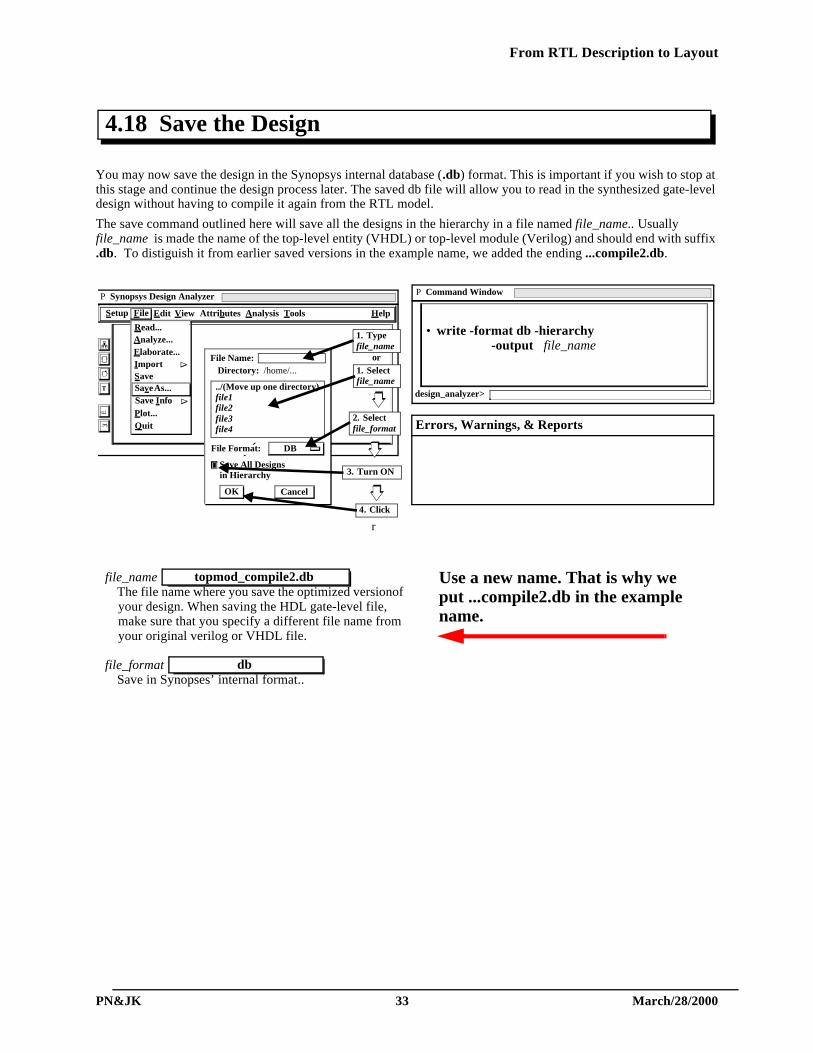
You may now save the design in the Synopsys internal database (.db) format. This is important if you wish to stop at this stage and continue the design process later. The saved db file will allow you to read in the synthesized gate-level design without having to compile it again from the RTL model.
The save command outlined here will save all the designs in the hierarchy in a file named file_name.. Usually file_name is made the name of the top-level entity (VHDL) or top-level module (Verilog) and should end with suffix .db. To distiguish it from earlier saved versions in the example name, we added the ending ...compile2.db.
4.18 Save the Design
P Command Window
• write -format db -hierarchy -output file_name ↵
design_analyzer>
Errors, Warnings, & Reports
P Synopsys Design Analyzer
È
È
T
File Edit View Attributes Analysis Tools Help Setup
File Name:Directory: /home/...
Save All Designsin Hierarchy
File Format:
../(Move up one directory)file1file2file3file4
DB
OK Cancel
Read...Analyze...Elaborate...
SaveSave As... Save Info ∆
Plot... Quit
Import ∆
4. Click
r
1. Typefile_name
1. Selectfile_name
2. Selectfile_format
or
3. Turn ON
file_name The file name where you save the optimized versionof your design. When saving the HDL gate-level file, make sure that you specify a different file name from your original verilog or VHDL file.
file_format Save in Synopses’ internal format..
topmod_compile2.db Use a new name. That is why weput ...compile2.db in the examplename.
db
From RTL Description to Layout
PN&JK 34 March/28/2000
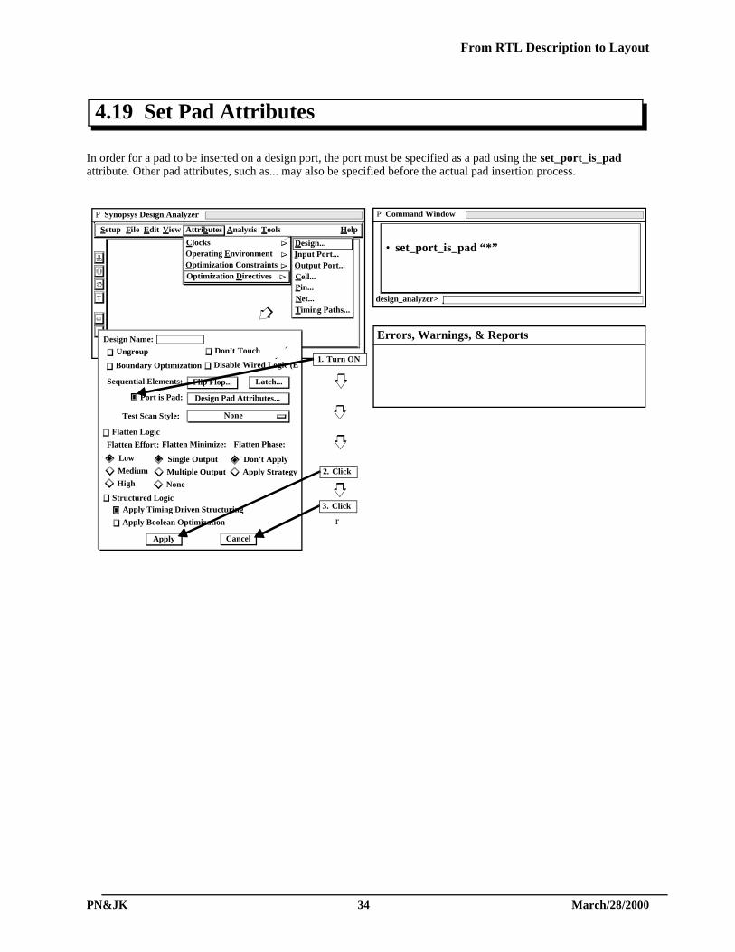
In order for a pad to be inserted on a design port, the port must be specified as a pad using the set_port_is_pad attribute. Other pad attributes, such as... may also be specified before the actual pad insertion process.
4.19 Set Pad Attributes
P Synopsys Design Analyzer
È
È
T
P Command Window
• set_port_is_pad “*”↵
design_analyzer>
Errors, Warnings, & Reports
File Edit View Attributes Analysis Tools Help Setup
Design...Input Port...Output Port...Cell...Pin... Net...Timing Paths...
2. Click
3. Click
ClocksOperating EnvironmentOptimization ConstraintsOptimization Directives
∆
∆
∆
∆
Design Name:
Flatten Effort:
CancelApply
Structured Logic
Low
Boundary Optimization
Port is Pad:
Ungroup
Disable Wired Logic (E
Single Output
Flatten Minimize: Flatten Phase:
Don’t ApplyMedium Multiple Output Apply StrategyHigh None
Flatten Logic
Don’t Touch
Test Scan Style: None
Design Pad Attributes...
Apply Timing Driven Structuring
Apply Boolean Optimization
Sequential Elements: Latch...Flip Flop...
r
1. Turn ON
From RTL Description to Layout
PN&JK 35 March/28/2000
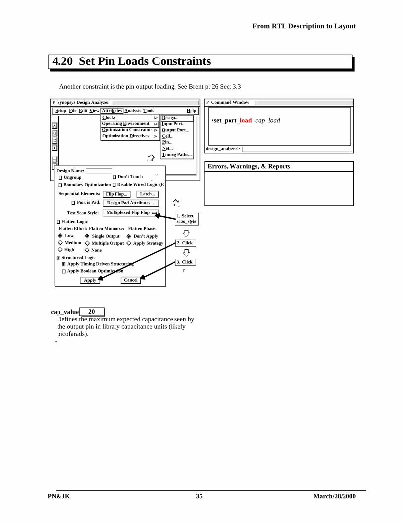
Another constraint is the pin output loading. See Brent p. 26 Sect 3.3
4.20 Set Pin Loads Constraints
P Synopsys Design Analyzer
È
È
T
P Command Window
•set_port_load cap_load↵
design_analyzer>
cap_valueDefines the maximum expected capacitance seen by the output pin in library capacitance units (likely picofarads).
-
20
Errors, Warnings, & Reports
Design...Input Port...Output Port...Cell...Pin... Net...Timing Paths...
1. Selectscan_style
2. Click
3. Click
File Edit View Attributes Analysis Tools Help Setup
ClocksOperating EnvironmentOptimization ConstraintsOptimization Directives
∆
∆
∆
∆
Design Name:
Flatten Effort:
CancelApply
Structured Logic
Low
Boundary Optimization
Port is Pad:
Ungroup
Disable Wired Logic (E
Single Output
Flatten Minimize: Flatten Phase:
Don’t ApplyMedium Multiple Output Apply StrategyHigh None
Flatten Logic
Don’t Touch
Test Scan Style: Multiplexed Flip Flop
Design Pad Attributes...
Apply Timing Driven Structuring
Apply Boolean Optimization
Sequential Elements: Latch...Flip Flop...
r
From RTL Description to Layout
PN&JK 36 March/28/2000
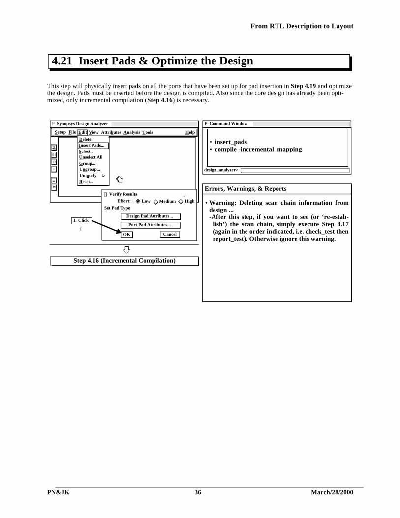
This step will physically insert pads on all the ports that have been set up for pad insertion in Step 4.19 and optimize the design. Pads must be inserted before the design is compiled. Also since the core design has already been opti-mized, only incremental compilation (Step 4.16) is necessary.
4.21 Insert Pads & Optimize the Design
• Warning: Deleting scan chain information fromdesign ...-After this step, if you want to see (or ‘re-estab-
lish’) the scan chain, simply execute Step 4.17(again in the order indicated, i.e. check_test thenreport_test). Otherwise ignore this warning.
P Synopsys Design Analyzer
È
È
T
P Command Window
• insert_pads↵ • compile -incremental_mapping↵
design_analyzer>
Errors, Warnings, & Reports
File Edit View Attributes Analysis Tools Help Setup
DeleteInsert Pads...Select...
Group...Ungroup... Uniquify ∆
Reset...
Unselect All
Cancel
Set Pad Type
Design Pad Attributes...
Effort:
Verify Results
Low Medium High
OK
Port Pad Attributes...r
1. Click
Step 4.16 (Incremental Compilation)
From RTL Description to Layout
PN&JK 37 March/28/2000
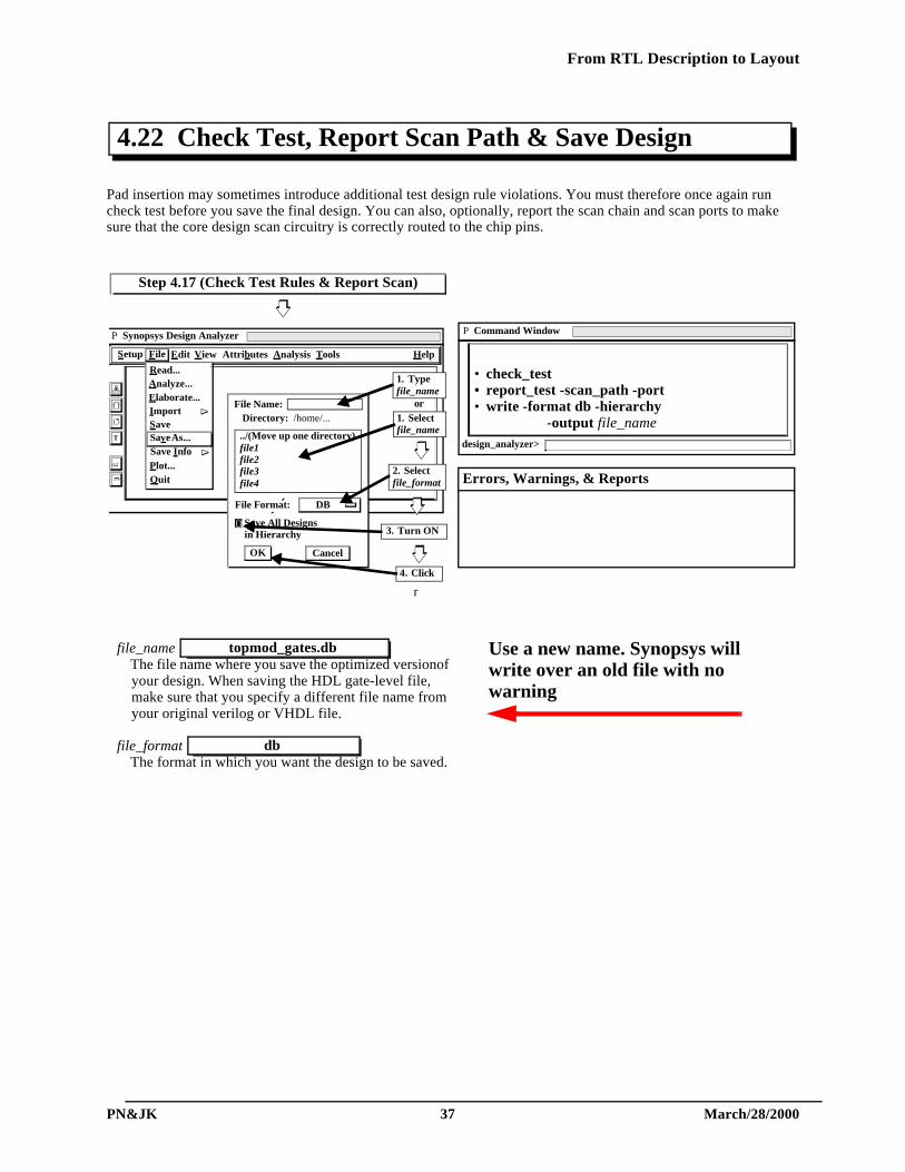
Pad insertion may sometimes introduce additional test design rule violations. You must therefore once again run check test before you save the final design. You can also, optionally, report the scan chain and scan ports to make sure that the core design scan circuitry is correctly routed to the chip pins.
4.22 Check Test, Report Scan Path & Save Design
P Command Window
• check_test↵• report_test -scan_path -port↵• write -format db -hierarchy
-output file_name↵design_analyzer>
Errors, Warnings, & Reports
Step 4.17 (Check Test Rules & Report Scan)
P Synopsys Design Analyzer
È
È
T
File Edit View Attributes Analysis Tools Help Setup
File Name:Directory: /home/...
Save All Designsin Hierarchy
File Format:
../(Move up one directory)file1file2file3file4
DB
OK Cancel
Read...Analyze...Elaborate...
SaveSave As... Save Info ∆
Plot... Quit
Import ∆
4. Click
r
1. Typefile_name
1. Selectfile_name
2. Selectfile_format
or
3. Turn ON
file_name The file name where you save the optimized versionof your design. When saving the HDL gate-level file, make sure that you specify a different file name from your original verilog or VHDL file.
file_format The format in which you want the design to be saved.
topmod_gates.db Use a new name. Synopsys willwrite over an old file with nowarning
db
From RTL Description to Layout
PN&JK 38 March/28/2000
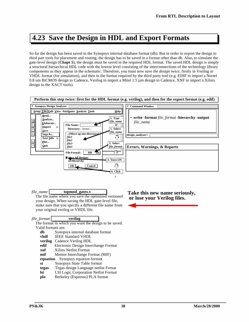
So far the design has been saved in the Synopsys internal database format (db). But in order to export the design to third part tools for placement and routing, the design has to be saved in a format other than db. Also, to simulate the gate-level design (Chapt 5), the design must be saved in the required HDL format. The saved HDL design is simply a structural hierarchical HDL code with the lowest level consisting of the interconnections of the technology library components as they appear in the schematic. Therefore, you must now save the design twice, firstly in Verilog or VHDL format (for simulation), and then in the format required by the third party tool (e.g. EDIF to import a Nortel 0.8 um BiCMOS design to Cadence, Verilog to import a Mitel 1.5 µm design to Cadence, XNF to import a Xilinx design to the XACT tools).
4.23 Save the Design in HDL and Export Formats
P Synopsys Design Analyzer
È
È
T
File Edit View Attributes Analysis Tools Help Setup
P Command Window
• write -format file_format -hierarchy -output file_name↵
design_analyzer>
file_name The file name where you save the optimized versionof your design. When saving the HDL gate-level file, make sure that you specify a different file name from your original verilog or VHDL file.
file_format The format in which you want the design to be saved. Valid formats are:
db Synopsys internal database formatvhdl IEEE Standard VHDLverilog Cadence Verilog HDLedif Electronic Design Interchange Formatxnf Xilinx Netlist Formatmif Mentor Interchange Format (MIF)equation Synopsys equation formatst Synopsys State Table formattegas Tegas design Language netlist Fornatlsi LSI Logic Corporation Netlist Formatpla Berkeley (Espresso) PLA format
topmod_gates.v Take this new name seriously, or lose your Verilog files.
verilog
Errors, Warnings, & Reports
File Name:Directory: /home/...
Save All Designsin Hierarchy
File Format:
../(Move up one directory)file1file2file3file4
DB
OK Cancel
Read...Analyze...Elaborate...
SaveSave As... Save Info ∆
Plot... Quit
Import ∆
4. Click
r
1. Typefile_name
1. Selectfile_name
2. Selectfile_format
or
3. Turn ON
Perform this step twice: first for the HDL format (e.g. verilog), and then for the export format (e.g. edif)
From RTL Description to Layout
PN&JK 39 March/28/2000
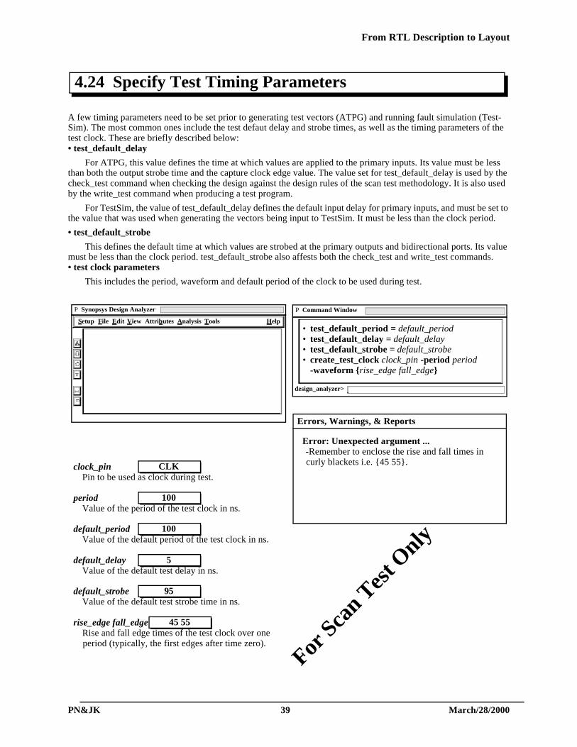
A few timing parameters need to be set prior to generating test vectors (ATPG) and running fault simulation (Test-Sim). The most common ones include the test defaut delay and strobe times, as well as the timing parameters of the test clock. These are briefly described below:• test_default_delay
For ATPG, this value defines the time at which values are applied to the primary inputs. Its value must be less than both the output strobe time and the capture clock edge value. The value set for test_default_delay is used by the check_test command when checking the design against the design rules of the scan test methodology. It is also used by the write_test command when producing a test program.
For TestSim, the value of test_default_delay defines the default input delay for primary inputs, and must be set to the value that was used when generating the vectors being input to TestSim. It must be less than the clock period.
• test_default_strobe
This defines the default time at which values are strobed at the primary outputs and bidirectional ports. Its value must be less than the clock period. test_default_strobe also affests both the check_test and write_test commands.• test clock parameters
This includes the period, waveform and default period of the clock to be used during test.
4.24 Specify Test Timing Parameters
P Command Window
• test_default_period = default_period↵• test_default_delay = default_delay↵• test_default_strobe = default_strobe↵• create_test_clock clock_pin -period period
-waveform {rise_edge fall_edge}↵
design_analyzer>
clock_pin Pin to be used as clock during test.
periodValue of the period of the test clock in ns.
default_periodValue of the default period of the test clock in ns.
default_delayValue of the default test delay in ns.
default_strobeValue of the default test strobe time in ns.
rise_edge fall_edgeRise and fall edge times of the test clock over one period (typically, the first edges after time zero).
CLK
100
100
5
95
45 55
Error: Unexpected argument ...-Remember to enclose the rise and fall times in curly blackets i.e. {45 55}.
Errors, Warnings, & Reports
P Synopsys Design Analyzer
È
È
T
File Edit View Attributes Analysis Tools Help Setup
For Sca
n Tes
t Only
From RTL Description to Layout
PN&JK 40 March/28/2000
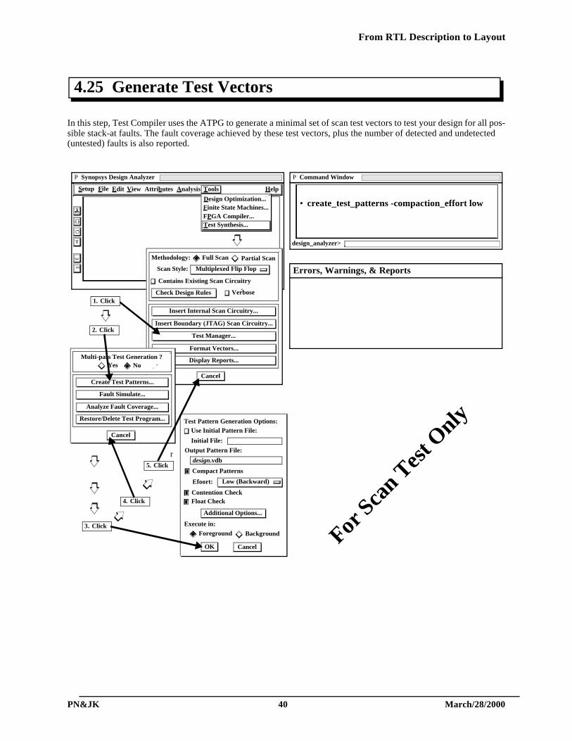
In this step, Test Compiler uses the ATPG to generate a minimal set of scan test vectors to test your design for all pos-sible stack-at faults. The fault coverage achieved by these test vectors, plus the number of detected and undetected (untested) faults is also reported.
4.25 Generate Test Vectors
P Synopsys Design Analyzer
È
È
T
P Command Window
• create_test_patterns -compaction_effort low↵
design_analyzer>
Errors, Warnings, & Reports
Cancel
VerboseCheck Design Rules
Contains Existing Scan Circuitry
Methodology: Full Scan Partial Scan
Scan Style: Multiplexed Flip Flop
Insert Internal Scan Circuitry...
Insert Boundary (JTAG) Scan Circuitry...
Test Manager...
Format Vectors...
Display Reports...
5. Click
r
1. Click
4. Click
File Edit View Attributes Analysis Tools Help Setup
Design Optimization...Finite State Machines...FPGA Compiler...Test Synthesis...
Cancel
Create Test Patterns...
Fault Simulate...
Analyze Fault Coverage...
Restore/Delete Test Program...
Multi-pass Test Generation ?Yes No
Cancel
Compact Patterns
Additional Options...
Execute in:
Foreground Background
OK
Test Pattern Generation Options:Use Initial Pattern File:
Initial File:
Output Pattern File:
design.vdb
Contention CheckFloat Check
Efoort: Low (Backward)
2. Click
3. Click
For Sca
n Tes
t Only
From RTL Description to Layout
PN&JK 41 March/28/2000
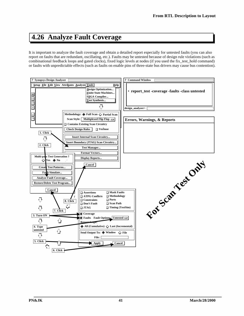
It is important to analyze the fault coverage and obtain a detailed report especially for untested faults (you can also report on faults that are redundant, oscillating, etc.). Faults may be untested because of design rule violations (such as combinational feedback loops and gated clocks), fixed logic levels at nodes (if you used the fix_test_hold command) or faults with unpredictable effects (such as faults on enable pins of three-state bus drivers may cause bus contention).
4.26 Analyze Fault Coverage
P Synopsys Design Analyzer
È
È
T
P Command Window
• report_test -coverage -faults -class untested↵
design_analyzer>
Errors, Warnings, & Reports
Cancel
VerboseCheck Design Rules
Contains Existing Scan Circuitry
Methodology: Full Scan Partial Scan
Scan Style: Multiplexed Flip Flop
Insert Internal Scan Circuitry...
Insert Boundary (JTAG) Scan Circuitry...
Test Manager...
Format Vectors...
Display Reports...
8. Click
r
1. Click
7. Click
File Edit View Attributes Analysis Tools Help Setup
Design Optimization...Finite State Machines...FPGA Compiler...Test Synthesis...
Cancel
Create Test Patterns...
Fault Simulate...
Analyze Fault Coverage...
Restore/Delete Test Program...
Multi-pass Test Generation ?Yes No
2. Click
5. ClickCancelApply
Assertions
Coverage
ATPG ConflictsConstraintsDon’t Fault
Send Output To: Window File
File:
JTAG
Faults Fault Options: Untested
Mask FaultsMethodologyPortsScan Path
Timing (TestSim)
Report Scope:
All (Cumulative) Last (Incremental)
3. Turn ON
4. Typeuntested
6. Click
For Sca
n Tes
t Only
From RTL Description to Layout
PN&JK 42 March/28/2000
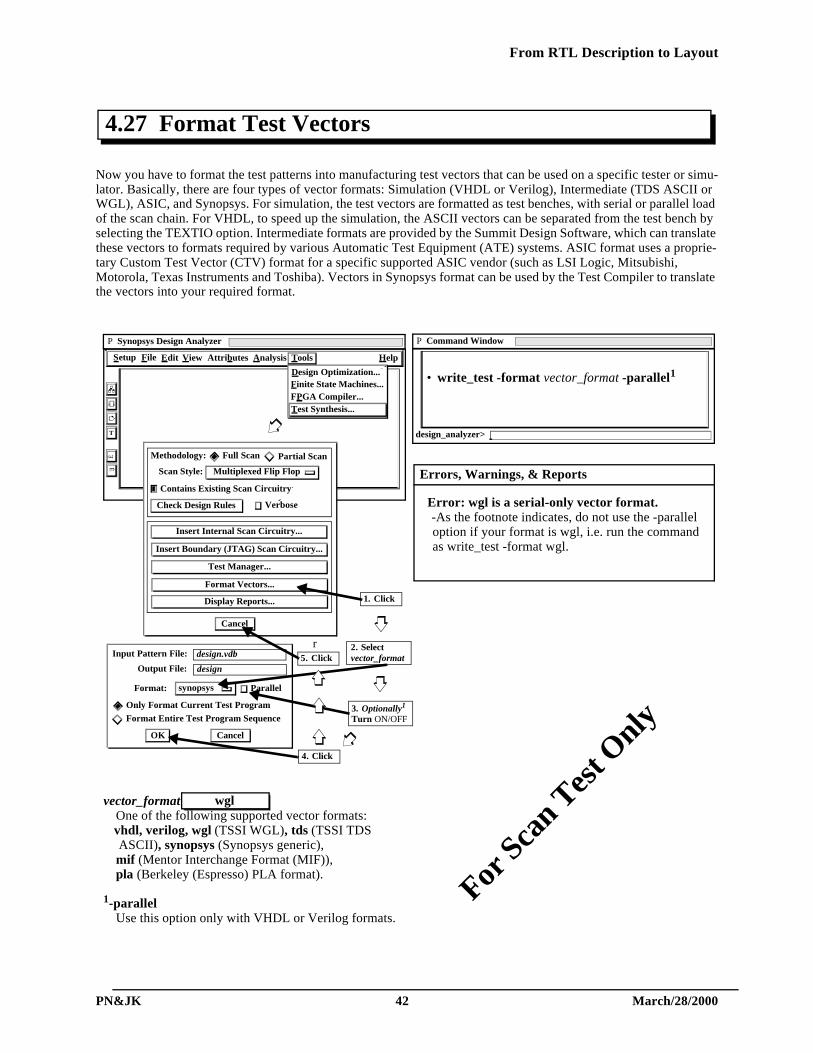
Now you have to format the test patterns into manufacturing test vectors that can be used on a specific tester or simu-lator. Basically, there are four types of vector formats: Simulation (VHDL or Verilog), Intermediate (TDS ASCII or WGL), ASIC, and Synopsys. For simulation, the test vectors are formatted as test benches, with serial or parallel load of the scan chain. For VHDL, to speed up the simulation, the ASCII vectors can be separated from the test bench by selecting the TEXTIO option. Intermediate formats are provided by the Summit Design Software, which can translate these vectors to formats required by various Automatic Test Equipment (ATE) systems. ASIC format uses a proprie-tary Custom Test Vector (CTV) format for a specific supported ASIC vendor (such as LSI Logic, Mitsubishi, Motorola, Texas Instruments and Toshiba). Vectors in Synopsys format can be used by the Test Compiler to translate the vectors into your required format.
4.27 Format Test Vectors
P Synopsys Design Analyzer
È
È
T
P Command Window
• write_test -format vector_format -parallel1↵
design_analyzer>
vector_formatOne of the following supported vector formats:vhdl, verilog, wgl (TSSI WGL), tds (TSSI TDS ASCII), synopsys (Synopsys generic),mif (Mentor Interchange Format (MIF)),pla (Berkeley (Espresso) PLA format).
1-parallelUse this option only with VHDL or Verilog formats.
wgl
Error: wgl is a serial-only vector format.-As the footnote indicates, do not use the -parallel option if your format is wgl, i.e. run the command as write_test -format wgl.
Errors, Warnings, & Reports
Cancel
VerboseCheck Design Rules
Contains Existing Scan Circuitry
Methodology: Full Scan Partial Scan
Scan Style: Multiplexed Flip Flop
Insert Internal Scan Circuitry...
Insert Boundary (JTAG) Scan Circuitry...
Test Manager...
Format Vectors...
Display Reports... 1. Click
4. Click
r5. Click
File Edit View Attributes Analysis Tools Help Setup
Design Optimization...Finite State Machines...FPGA Compiler...Test Synthesis...
Input Pattern File:
Parallel
Output File:
design.vdb
design
Format: synopsys
Only Format Current Test Program
Format Entire Test Program Sequence
OK Cancel
2. Selectvector_format
3. Optionally1
Turn ON/OFF
For Sca
n Tes
t Only
From RTL Description to Layout
PN&JK 43 March/28/2000
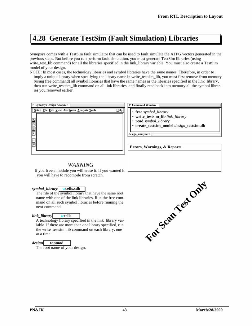
Synopsys comes with a TestSim fault simulator that can be used to fault simulate the ATPG vectors generated in the previous steps. But before you can perform fault simulation, you must generate TestSim libraries (using write_test_lib command) for all the libraries specified in the link_library variable. You must also create a TestSim model of your design.NOTE: In most cases, the technology libraries and symbol libraries have the same names. Therefore, in order to
imply a unique library when specifying the library name in write_testsim_lib, you must first remove from memory (using free command) all symbol libraries that have the same names as the libraries specified in the link_library, then run write_testsim_lib command on all link libraries, and finally read back into memory all the symbol librar-ies you removed earlier.
4.28 Generate TestSim (Fault Simulation) Libraries
P Command Window
• free symbol_library↵• write_testsim_lib link_library↵• read symbol_library↵• create_testsim_model design_testsim.db↵
design_analyzer>
WARNINGIf you free a module you will erase it. If you wanted it
you will have to recompile from scratch.
symbol_libraryThe file of the symbol library that have the same root name with one of the link libraries. Run the free com-mand on all such symbol libraries before running the next command.
link_libraryA technology library specified in the link_library var-iable. If there are more than one library specified, run the write_testsim_lib command on each library, one at a time.
designThe root name of your design.
wcells.sdb
wcells
topmod
Errors, Warnings, & Reports
P Synopsys Design Analyzer
È
È
T
File Edit View Attributes Analysis Tools Help Setup
For Sca
n Tes
t Only
From RTL Description to Layout
PN&JK 44 March/28/2000
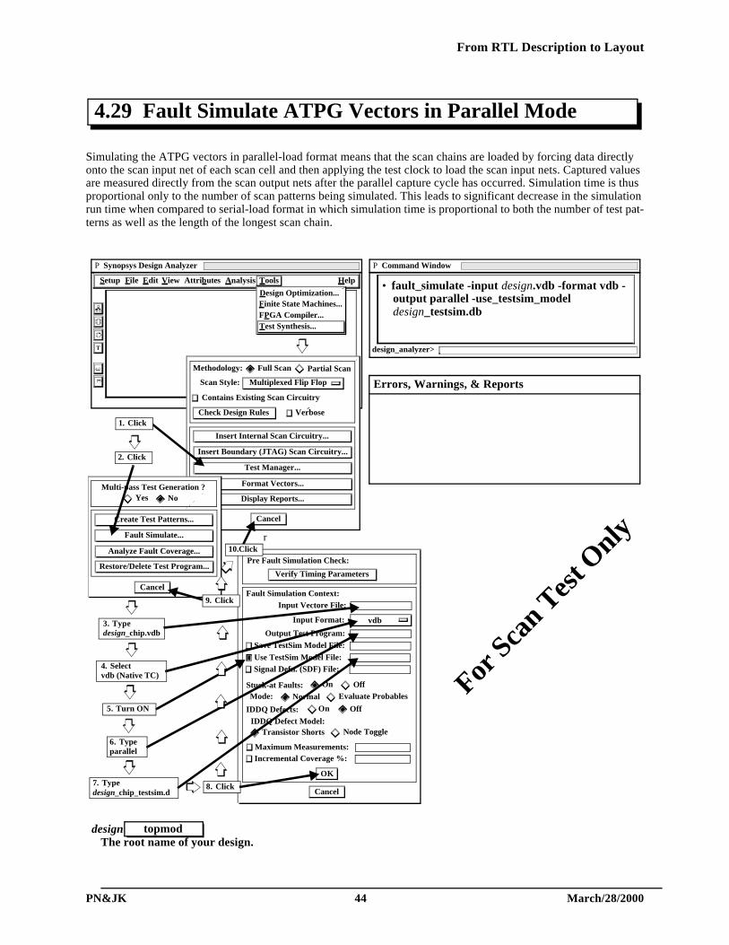
Simulating the ATPG vectors in parallel-load format means that the scan chains are loaded by forcing data directly onto the scan input net of each scan cell and then applying the test clock to load the scan input nets. Captured values are measured directly from the scan output nets after the parallel capture cycle has occurred. Simulation time is thus proportional only to the number of scan patterns being simulated. This leads to significant decrease in the simulation run time when compared to serial-load format in which simulation time is proportional to both the number of test pat-terns as well as the length of the longest scan chain.
4.29 Fault Simulate ATPG Vectors in Parallel Mode
P Synopsys Design Analyzer
È
È
T
P Command Window
• fault_simulate -input design.vdb -format vdb -output parallel -use_testsim_model design_testsim.db↵
design_analyzer>
designThe root name of your design.
topmod
Errors, Warnings, & Reports
Cancel
VerboseCheck Design Rules
Contains Existing Scan Circuitry
Methodology: Full Scan Partial Scan
Scan Style: Multiplexed Flip Flop
Insert Internal Scan Circuitry...
Insert Boundary (JTAG) Scan Circuitry...
Test Manager...
Format Vectors...
Display Reports...
r
1. Click
File Edit View Attributes Analysis Tools Help Setup
Design Optimization...Finite State Machines...FPGA Compiler...Test Synthesis...
Cancel
Create Test Patterns...
Fault Simulate...
Analyze Fault Coverage...
Restore/Delete Test Program...
Multi-pass Test Generation ?Yes No
2. Click
5. Turn ON
7. Typedesign_chip_testsim.d Cancel
Fault Simulation Context:
Input Format: vdb
Save TestSim Model File:
Verify Timing Parameters
Pre Fault Simulation Check:
Use TestSim Model File:Signal Defn. (SDF) File:
Input Vectore File:
Output Test Program:
Stuck-at Faults: On OffMode: Normal Evaluate Probables
IDDQ Defect Model:Transistor Shorts Node Toggle
IDDQ Defects: On Off
Maximum Measurements:Incremental Coverage %:
OK
9. Click
10.Click
3. Typedesign_chip.vdb
4. Selectvdb (Native TC)
6. Typeparallel
8. Click
For Sca
n Tes
t Only

From RTL Description to Layout
PN&JK 45 March/28/2000
In this step, you analyze the fault coverage produced by the TestSim (parallel-load) and then compare it to that pro-duced by Test Compiler. Therefore after analyzing the TestSim fault coverage (and recording the results), you must restore the test status to the state after ATPG, and then analyze fault coverage again and record the results.
4.30 Compare TestSim & Test Compiler Fault Coverage
P Synopsys Design Analyzer
È
È
T
P Command Window
• report_test -coverage -faults -class untested↵• restore_test design.vdb↵• report_test -coverage -faults -class untested↵
design_analyzer>
designThe root name of your design.
topmod
Errors, Warnings, & Reports
Cancel
VerboseCheck Design Rules
Contains Existing Scan Circuitry
Methodology: Full Scan Partial Scan
Scan Style: Multiplexed Flip Flop
Insert Internal Scan Circuitry...
Insert Boundary (JTAG) Scan Circuitry...
Test Manager...
Format Vectors...
Display Reports...
r
1. Click
File Edit View Attributes Analysis Tools Help Setup
Design Optimization...Finite State Machines...FPGA Compiler...Test Synthesis...
Cancel
Create Test Patterns...
Fault Simulate...
Analyze Fault Coverage...
Restore/Delete Test Program...
Multi-pass Test Generation ?Yes No
2. Click
3. Turn ON
8. Click
4. Typedesign_chip.vdb
5. Click
CancelApply
Name:Restore Test Program
delete Current Test Program
7. Click
6. Click
Step 4.26 (Analyze Fault Coverage)
Step 4.26 (Analyze Fault Coverage)
For Sca
n Tes
t Only
From RTL Description to Layout
PN&JK 46 March/28/2000
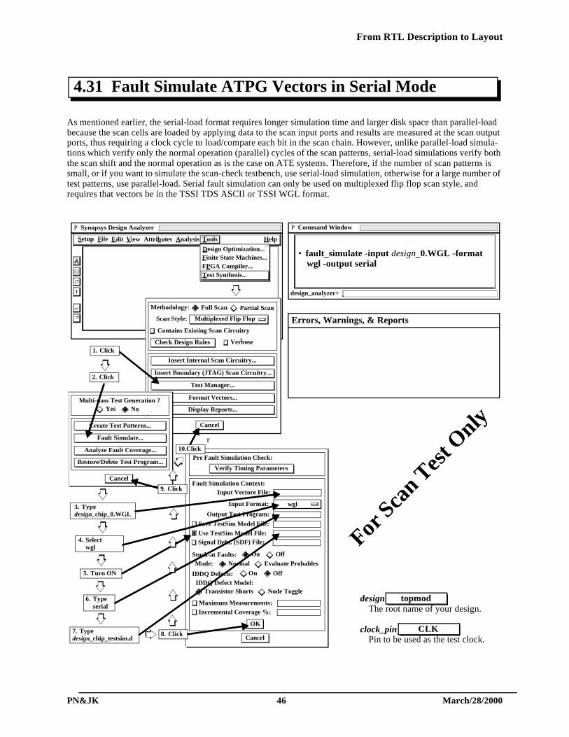
As mentioned earlier, the serial-load format requires longer simulation time and larger disk space than parallel-load because the scan cells are loaded by applying data to the scan input ports and results are measured at the scan output ports, thus requiring a clock cycle to load/compare each bit in the scan chain. However, unlike parallel-load simula-tions which verify only the normal operation (parallel) cycles of the scan patterns, serial-load simulations verify both the scan shift and the normal operation as is the case on ATE systems. Therefore, if the number of scan patterns is small, or if you want to simulate the scan-check testbench, use serial-load simulation, otherwise for a large number of test patterns, use parallel-load. Serial fault simulation can only be used on multiplexed flip flop scan style, and requires that vectors be in the TSSI TDS ASCII or TSSI WGL format.
4.31 Fault Simulate ATPG Vectors in Serial Mode
P Synopsys Design Analyzer
È
È
T
P Command Window
• fault_simulate -input design_0.WGL -format wgl -output serial↵
design_analyzer>
designThe root name of your design.
clock_pinPin to be used as the test clock.
topmod
CLK
Errors, Warnings, & Reports
Cancel
VerboseCheck Design Rules
Contains Existing Scan Circuitry
Methodology: Full Scan Partial Scan
Scan Style: Multiplexed Flip Flop
Insert Internal Scan Circuitry...
Insert Boundary (JTAG) Scan Circuitry...
Test Manager...
Format Vectors...
Display Reports...
r
1. Click
File Edit View Attributes Analysis Tools Help Setup
Design Optimization...Finite State Machines...FPGA Compiler...Test Synthesis...
Cancel
Create Test Patterns...
Fault Simulate...
Analyze Fault Coverage...
Restore/Delete Test Program...
Multi-pass Test Generation ?Yes No
2. Click
5. Turn ON
7. Typedesign_chip_testsim.d Cancel
Fault Simulation Context:
Input Format: wgl
Save TestSim Model File:
Verify Timing Parameters
Pre Fault Simulation Check:
Use TestSim Model File:Signal Defn. (SDF) File:
Input Vectore File:
Output Test Program:
Stuck-at Faults: On Off
Mode: Normal Evaluate Probables
IDDQ Defect Model:Transistor Shorts Node Toggle
IDDQ Defects: On Off
Maximum Measurements:Incremental Coverage %:
OK
9. Click
10.Click
3. Typedesign_chip_0.WGL
4. Selectwgl
6. Typeserial
8. Click
For Sca
n Tes
t Only