synthesis strategies and a study of properties of … · 7.3.1 synthesis using electrolyte a ......
TRANSCRIPT

APPROVED: Usha Philipose, Major Professor Duncan Weathers, Committee Member Arup Neogi, Committee Member Chris Littler, Committee Member and
Chair of the Department of Physics
Mark Wardell, Dean of the Toulouse Graduate School
SYNTHESIS STRATEGIES AND A STUDY OF PROPERTIES OF NARROW
AND WIDE BAND GAP NANOWIRES
Gopal Sapkota
Dissertation Prepared for the Degree of
DOCTOR OF PHILOSOPHY
UNIVERSITY OF NORTH TEXAS
May 2014

Sapkota, Gopal. Synthesis Strategies and a Study of Properties of Narrow and
Wide Band Gap Nanowires. Doctor of Philosophy (Physics), 111 pp., 3 tables, 45
figures, bibliography, 172 titles.
Various techniques to synthesize nanowires and nanotubes as a function of
growth temperature and time were investigated. These include growth of nanowires by a
chemical vapor deposition (CVD) system using vapor-liquid-solid (VLS) growth
mechanism and electro-chemical synthesis of nanowires and nanotubes. Narrow band
gap InSb Eg = 0.17 eV at room temp) nanowires were successively synthesized. Using a
phase diagram, the transition of the nanowire from metallic- semiconducting- semi-
metallic phase was investigated. A thermodynamic model is developed to show that the
occurrence of native defects in InSb nanowires influenced by the nanowire growth
kinetics and thermodynamics of defect formation. Wide band gap ZnO (Eg = 3.34 eV)
and In2O3 (3.7 eV) were also synthesized. ZnO nanowires and nanotubes were
successfully doped with a transition metal Fe, making it a Dilute Magnetic
Semiconductor of great technological relevance. Structural and electronic
characterizations of nanowires were studied for different semiconducting, metallic and
semi-metallic nanowires. Electron transport measurements were used to estimate
intrinsic material parameters like carrier concentration and mobility. An efficient gas
sensing device using a single In2O3 nanowire was studied and which showed sensitivity
to reducing gas like NH3 and oxidizing gas like O2 gas at room temperature. The
efficiency of the gas sensing device was found to be sensitive to the nature of contacts as
well as the presence of surface states on the nanowire.

ii
Copyright 2014
by
Gopal Sapkota

iii
ACKNOWLEDGEMENTS
I would like to express my sincere gratitude to my advisor, Dr.Usha Philipose for
her continuous guidance, constructive suggestions and supervision throughout the
progress of this work. This work would never have been finished without her guidance,
constant encouragement, continuing support and patience. I would also like to thank my
committee members, Dr. Arup Neogi, Dr. Duncan Weathers and Dr. Chris Littler, for
their valuable suggestion, comments and encouragement for the completion of my
projects. I am also thankful to the Department of Physics for giving me the opportunity
to pursue Ph.D in my area of interest and financial support throughout the years
staying at the University of North Texas. I would like to thank all of my friends and
lab-mates; Pradeep Gali Prathyusha Nukala, Bhargav Mallampati and Kiran Shrestha
for the friendly feelings we shared while studying and doing research.
I would like to express my gratitude to my parents, grandparents, two younger
brothers, maternal uncles and all of my relatives who always motivated me to work hard
and pursue a Ph.D aboard. They always supported and encouraged me with their best
wishes.
I am greatly indebted to my wife and two daughters Taniska and Tejasee. Their
unconditional love and continuous support without any complain has enabled me to
complete my Ph.D. They were always there for cheering up and stood by me at each
and every second for years, through the good and bad times.
Finally, I would like to express my appreciation to the publishers i.e. Institute of
Physics (IOP) and Springer. All the content included in this manuscript from my
publication are used with their permission.
iv
TABLE OF CONTENTS
Page ACKNOWLEDGMENTS ............................................................................................... iii LIST OF TABLES ........................................................................................................ vii LIST OF FIGURES ..................................................................................................... viii CHAPTER 1 INTRODUCTION, GROWTH TECHNIQUES AND GROWTH MECHANISM OF NANOSTRUCTURES ...................................................................... 1
1.1 Introduction ............................................................................................... 1 1.2 Size Effects Affecting Material Properties .................................................. 5
1.2.1 3-Dimension (3-D) Density of States ............................................... 6 1.2.2 2-Dimension (2-D) Density of States ............................................... 6 1.2.3 1-Dimention (1-D) Density of States ............................................... 7 1.2.4 0-Dimension (0-D) Density of States ............................................... 7
1.3 Nanowire Growth Techniques .................................................................... 7 1.3.1 Physical Vapor Deposition (PVD) .................................................. 7 1.3.2 Chemical Vapor Deposition (CVD) ................................................. 9 1.3.3 Electrochemical Method .................................................................. 9
1.4 Nanowire Growth Mechanism ................................................................... 10 1.4.1 VLS Growth Process ...................................................................... 10
1.5 Focus of the Thesis and Layout ................................................................ 15 CHAPTER 2 SYNTHESIS OF INDIUM ANTIMONIDE NANOWIRES AND IRON DOPED ZINC OXIDE NANOWIRES AND NANOTUBES .......................................... 18
2.1 Synthesis of InSb Nanowires ..................................................................... 18 2.1.1 InSb Nanowires Using In as a Catalyst .......................................... 19 2.1.2 InSb Nanowires Using Au as a Catalyst ......................................... 19 2.1.3 Synthesis of InSb Nanowires in the Presence of Oxygen ................ 20
2.2 Electrochemical Synthesis of Fe Doped ZnO Nanowires and Nanotubes ... 21 2.2.1 Fe Doped ZnO Nanowires .............................................................. 21 2.2.2 Fe Doped ZnO Nanotubes .............................................................. 22 2.2.3 Diluted Magnetic Semiconductors (DMS) ...................................... 23

v
2.3 Size Effect and Quantum Confinement of As-grown Nanowires (ZnO, In2O3 and InSb) ....................................................................................... 24 2.3.1 Effect of Quantum Confinement on Band Gap for As-grown InSb
Nanowires ....................................................................................... 24 CHAPTER 3 INFLUENCE OF GROWTH TEMPERATURE ON THE STOICHIOMETRY OF INDIUM ANTIMONIDE NANOWIRES ................................. 27
3.1 Introduction .............................................................................................. 27 3.2 Experimental Details ................................................................................. 27 3.3 Structural Characterization ....................................................................... 28 3.4 Results and Discussion .............................................................................. 28 3.5 Electron Transport Measurements ............................................................ 35 3.6 Conclusion ................................................................................................. 39
CHAPTER 4 DEFECT FORMATION IN INDIUM ANTIMONIDE NANOWIRES AND ITS EFFECT ON STOICHIOMETRY AND CARRIER TRANSPORT ............. 40
4.1 Introduction .............................................................................................. 40 4.2 Experimental Details ................................................................................. 41 4.3 Structural Characterization ....................................................................... 41 4.4 Defect Analysis ......................................................................................... 42 4.5 Results and Discussion .............................................................................. 46 4.6 Electron Transport Measurements ............................................................ 52 4.7 Conclusion ................................................................................................. 56
CHAPTER 5 SYNTHESIS OF METALLIC, SEMICONDUCTING, AND SEMIMETALLIC NANOWIRES THROUGH CONTROL OF INDIUM ANTIMONIDE GROWTH PARAMETERS ........................................................................................... 57
5.1 Introduction .............................................................................................. 57 5.2 Temperature Dependence of Resistivity (ρ) .............................................. 58
5.2.1 Temperature Dependence of ρ for Semiconductor .......................... 58 5.2.2 Temperature Dependence of ρ for Metal ........................................ 59
5.3 Experimental Details ................................................................................. 59 5.4 Structural Characterization ....................................................................... 59 5.5 Results and Discussion .............................................................................. 60
5.5.1 Synthesis of InSb Nanowires .......................................................... 60

vi
5.5.2 Synthesis of In Nanowires .............................................................. 62 5.5.3 Synthesis of Sb Nanowires .............................................................. 64
5.6 Electron Transport Measurements ............................................................ 66 5.6.1 InSb Nanowires .............................................................................. 67 5.6.2 In Nanowires .................................................................................. 69 5.6.3 Sb Nanowires .................................................................................. 71
5.7 Conclusion ................................................................................................. 73 CHAPTER 6 INDIUM OXIDE NANOWIRES FOR GAS SENSING APPLICATION ....................................................................................................................................... 75
6.1 Introduction .............................................................................................. 75 6.2 Experimental Details ................................................................................. 75 6.3 Structural Characterization ....................................................................... 76 6.4 Results and Discussion .............................................................................. 76 6.5 Conclusions ............................................................................................... 82
CHAPTER 7 LOW TEMPERATURE SYNTHESIS OF IRON DOPED ZINC OXIDE NANOWIRES AND NANOTUBES ............................................................................... 83
7.1 Introduction .............................................................................................. 83 7.2 Experimental Details ................................................................................. 84 7.3 Results and Discussion .............................................................................. 85
7.3.1 Synthesis Using Electrolyte A ........................................................ 85 7.3.2 Synthesis Using Electrolyte B ........................................................ 87 7.3.3 Growth Mechanism of Nanotubes .................................................. 88
7.4 Conclusion ................................................................................................. 95 CHAPTER 8 CONCLUSION AND FUTURE WORKS ................................................ 97
8.1 Conclusion ................................................................................................. 97 8.2 Future Work ............................................................................................. 99
APPENDIX: LIST OF PUBLICATIONS .................................................................... 100 BIBLIOGRAPHY ......................................................................................................... 102
vii
LIST OF TABLES
Page 3.1 Growth parameters and morphology/composition of the nanostructures grown
using Au-In film ................................................................................................... 32
4.1 Equilibrium constants derived from reaction equations ....................................... 43
5.1 Experimental conditions used in the synthesis of InSb, In and Sb nanowires ...... 59
viii
LIST OF FIGURES
Page
1.1 Plot of nominal feature size for transistors as a function of time [127] ................. 2
1.2 Density of states ................................................................................................... 8
1.3 Schematic of experimental setup of CVD system for the growth of different nanowires ............................................................................................................. 10
1.4 Schematic of electrochemical cell ......................................................................... 11
1.5 Schematic representation of VLS mechanism....................................................... 12
1.6 Phase diagram of the Au-Si system [137] ............................................................. 13
1.7 Growth of nanowires with respect to size of the catalyst ..................................... 15
2.1 InSb phase diagram ............................................................................................. 20
2.2 Ternary phase diagram of Au-In-Sb [81] .............................................................. 21
2.3 Basic band structure layout in InSb .................................................................... 26
3.1 (a) SEM image of thick Sb rich nanostructures; (b) EDX spectrum confirming that the nanostructures mostly comprise Sb ........................................................ 29
3.2 (a) SEM image of the InSb nanowires; (b) EDX analysis confirm the stoichiometric composition of the InSb nanowires ............................................... 31
3.4 SEM image of the tapered InSb nanowires grown at a source temperature of 650°C and a substrate temperature of 510°C ....................................................... 32
3.5 EDX spectrum of InSb nanowires grown at 530°C .............................................. 33
3.6 (a) EDX spectrum of In nanowires grown at 600°C; (b) HRTEM image of the In nanowires confirming their crystalline nature ...................................................... 34
3.7 (a) Dependence of measured current I on applied voltage Va between outer terminals and measured voltage between inner two terminals; (b) Dependence of conductance G=I/V on temperature ................................................................... 37
3.8 Dependence of InSb nanowire conductance on back-gate voltage ........................ 38
4.1 Vacancy defect concentrations in InSb nanowires ................................................ 45
4.2 Sum of defect concentration variation ................................................................. 46

ix
4.3 SEM image of InSb nanowires that grow from 100200 nm-sized In droplets ...... 47
4.4 (a) SEM image of a 40 nm thick InSb nanowire grown at 450°C; (b) EDX spectrum of the InSb nanowire with a composition ratio of 60 at% In:40 at% Sb48
4.5 SEM image and elemental mapping showing the stoichiometry of an InSb nanowire grown at 526°C ..................................................................................... 49
4.6 HRTEM image of a single InSb nanowire, with a lattice constant of about 0.67 nm ....................................................................................................................... 50
4.7 (a) SEM image and elemental map of a single 50 nm thick In nanowire; (b) EDX spectrum obtained from the In nanowire ............................................................. 51
4.8 Variation of drain-source current (Ids) with drain-source voltage (Vds) at zero gate bias for a single InSb nanowire .................................................................... 53
4.9 Results of electron transport measurements on an In-rich InSb nanowires .......... 54
4.10 Variation of drain-source current (Ids) with drain-source voltage (Vds) at zero gate bias for a single In nanowire ........................................................................ 55
5.1 Structure and composition of InSb nanowires ...................................................... 61
5.2 Raman spectrum for InSb, In and Sb nanowires, measured at room temperature63
5.3 Structure and composition of In nanowires .......................................................... 64
5.4 Structure and composition of Sb nanowires ......................................................... 65
5.5 Electron transport and temperature dependent resistance measurements on a 50 nm thick InSb nanowire ....................................................................................... 68
5.6 Electron transport and temperature dependence measurements on a 40 nm thick In nanowire .......................................................................................................... 70
5.7 Electron transport and temperature dependence measurements on a 40 nm thick Sb nanowire ......................................................................................................... 72
6.1 (a) SEM image of the In2O3 nanowires; (b) EDX analysis confirms the nearly stoichiometric composition of the In2O3 nanowires ............................................. 78
6.3 (a) Sensing response for device B for 10 ppm NH3 gas at room temperature; (b) Sensing response for device B for10 ppm O2 gas at room temperature ................ 79
6.4 In2O3 nanowire gas sensor response as NH3 molecules are desorbed from the nanowire surface .................................................................................................. 80

x
6.5 Schematic of gas sensing mechanism explained in terms of energy band diagram81
7.1 SEM image of nanotubes grown using electrolyte A for 90 minutes .................... 86
7.2 SEM image of Fe doped ZnO nanorods grown using electrolyte A for 45 minutes87
7.3 SEM image of Fe doped ZnO nanorods grown using electrolyte B for 90 minutes88
7.4 HRTEM images of Fe doped ZnO nanotube ........................................................ 90
7.5 XRD spectrum of undoped (solid line) and Fe doped (dotted line) ZnO nanotubes92
7.6 Room temperature PL spectra of undoped and Fe doped ZnO nanotubes........... 94
7.7 Raman scattering spectrum for (a) undoped ZnO nanotubes and (b) Fe doped ZnO nanotubes .................................................................................................... 95
CHAPTER 1
INTRODUCTION, GROWTH TECHNIQUES AND GROWTH MECHANISM OF
NANOSTRUCTURES
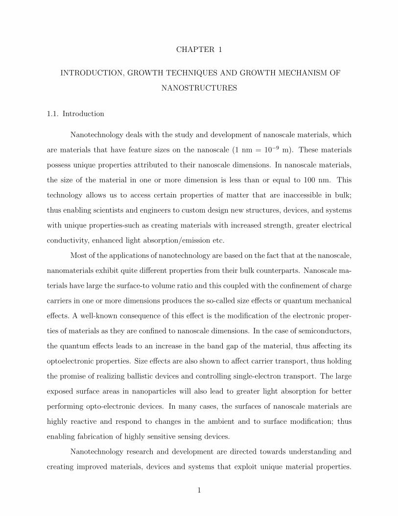
1.1. Introduction
Nanotechnology deals with the study and development of nanoscale materials, which
are materials that have feature sizes on the nanoscale (1 nm = 10−9 m). These materials
possess unique properties attributed to their nanoscale dimensions. In nanoscale materials,
the size of the material in one or more dimension is less than or equal to 100 nm. This
technology allows us to access certain properties of matter that are inaccessible in bulk;
thus enabling scientists and engineers to custom design new structures, devices, and systems
with unique properties-such as creating materials with increased strength, greater electrical
conductivity, enhanced light absorption/emission etc.
Most of the applications of nanotechnology are based on the fact that at the nanoscale,
nanomaterials exhibit quite different properties from their bulk counterparts. Nanoscale ma-
terials have large the surface-to volume ratio and this coupled with the confinement of charge
carriers in one or more dimensions produces the so-called size effects or quantum mechanical
effects. A well-known consequence of this effect is the modification of the electronic proper-
ties of materials as they are confined to nanoscale dimensions. In the case of semiconductors,
the quantum effects leads to an increase in the band gap of the material, thus affecting its
optoelectronic properties. Size effects are also shown to affect carrier transport, thus holding
the promise of realizing ballistic devices and controlling single-electron transport. The large
exposed surface areas in nanoparticles will also lead to greater light absorption for better
performing opto-electronic devices. In many cases, the surfaces of nanoscale materials are
highly reactive and respond to changes in the ambient and to surface modification; thus
enabling fabrication of highly sensitive sensing devices.
Nanotechnology research and development are directed towards understanding and
creating improved materials, devices and systems that exploit unique material properties.
1

Miniaturization of electronic devices is one of the main goals of the semiconductor industry
today. The fast pace of semiconductor market emerging with these small and energy effi-
cient nanostructure products has forced the semiconductor industry to follow this pace with
research and development directed towards device scaling (Figure 1.1 [127]). Moores law
Figure 1.1. Plot of nominal feature size for transistors as a function of time [127].
has been the guiding force promoting development of microprocessors with higher density,
faster speed and lower power consumption. This is done by shrinking device feature sizes,
introducing low-dimensional materials and active device components.
There are different types of nanostructure based on the dimensions of their structural
elements: zero-dimensional (0-D), one-dimensional (1-D), two-dimensional (2-D) and three-
dimensional (3-D) nanostructure. 0-D nanostructure include quantum dots which has been
extensively studied in light emitting diodes (LEDs) [67], solar cells [140], single-electron tran-
2

sistors [138], and lasers [139]. 1-D nanostructures include nanowires, nanorods, nanotubes,
nanobelts, and nanoribbons, and are considered to have promising application both as in-
terconnects and the key units in electronic and optoelectronic devices. 2-D nanostructures
include quantum wells and thin films with nanometer thickness, nanoprisms, nanoplates,
nanosheets, nanowalls, and nanodisks which have been used in several novel applications
such as in sensors, photocatalysts, nanocontainers, nanoreactors etc. 3-D nanostructures
include nanocoils, nanocones, etc, that have been used in a wide range of applications area
including magnetic materials and electrode material for batteries [25, 148].
Considering the focus of technology on the development of miniaturized devices, it
is imperative that nanoscale materials be developed using simple, new and cost-efficient
fabrication processes that will allow precise control over size and morphology of the nanos-
tructure. The ultimate goal of nanoscale material synthesis is the development as functional
devices that will help improve existing technologies, and provide better performing devices.
The promise of nanotechnology lies in its potential to provide sustainable alternatives in
fields like medicine, electronics, energy production, and computing.
This thesis focuses on the development and characterization of two types of materi-
als: (i) narrow band gap material like indium antimonide (InSb), and (ii) wide band gap
materials like indium oxide ( In2O3) and zinc oxide (ZnO).
The first part of this thesis is devoted to the development of a successful synthesis
strategy for the growth of InSb nanowires which is an attractive candidate for the fabri-
cation of infra-red (IR) detectors. A promising result of this work is the demonstration of
fabrication of high-quality metallic, semiconducting and semi-metallic nanowires within the
framework of the same growth process. Thus, by tuning the growth parameter during the
growth of InSb nanowire, it was possible to synthesize metallic indium (In), semiconducting
InSb and semi-metallic antimony (Sb) nanowires. Indium nanowires can be used as both
interconnects and as functional units in nanoscale electronic, opto-electronic and electro-
chemical devices. Sb nanowires are promising as good thermoelectric materials.
The second part of this thesis focuses on the synthesis and study of metal-oxide
3

nanowires like In2O3 and ZnO. Through this work, the efficiency of a single In2O3 nanowire
as a gas sensor is demonstrated. A significant achievement is the synthesis of transition
metal (Fe) doped ZnO nanowires and nanotubes using a low temperature electrochemical
method. Fe doped ZnO is a promising dilute magnetic semiconductor and especially with
application in spin based electronics-spintronics. The following are the reasons behind the
study of these materials:
(I) InSb: InSb is a promising III–V direct band gap semiconductor (0.17 eV at 300
K) with high electron mobility (7.8 × 104 cm2V−2 s−1 at 300K) and small effective mass.
InSb nanowires, with a huge exciton Bohr radius (60nm) can provide one-dimensional quan-
tization effects at relatively large diameter of the nanowires. The high carrier mobility, low
effective mass, and low (direct) band gap make InSb suitable for use in applications such
as high-speed, low-power transistors, tunneling field-effect transistors, photo detector (suc-
cessful demonstration will find applications in medicine, fire detection, communication and
astronomy), magnetic field sensors, and thermoelectric power generation [125].
(II) In2O3: In2O3, a transparent conducting semiconductor with a direct band gap
of 3.7 eV and indirect band gap of 2.6 eV, has been used extensively in microelectronic
applications, such as window heaters, solar cells and flat-panel displays [57]. The motiva-
tion behind the study of In2O3 nanowires is its gas sensing application due to their high
surface-to-volume ratio which increases sensitivity and response of the sensor to changing
environments.
(III )ZnO: ZnO is a II-VI direct wide band gap semiconductor, with unique and in-
teresting properties such as a relatively high exciton binding energy (60 meV), wide band
gap (3.34eV), and piezoelectric properties. The interest behind ZnO is due to the possibility
of making low-energy, environmentally friendly light-emitting devices and laser diodes [167]
operating above room temperature. In addition, doping ZnO nanowires and nanotubes with
transition element draws considerable attention as a Dilute Magnetic Semiconductor (DMS)
for potential spintronics device application.
4
1.2. Size Effects Affecting Material Properties
A material’s properties changes significantly compared to its bulk counterpart when
its length in any one dimension or more is reduced to nanoscale (1–100 nm). The material
is said to possess size dependent properties in this scale range. At this size scale, quantum
effects rule the behavior and properties of the materials. Thus, the intrinsic properties of a
material -like its melting point, fluorescence, electrical conductivity, magnetic permeability,
and chemical reactivity become a function of the size of the particle. The fascinating aspect
of quantum effects is the concept of tunability of properties. As a result, one can fine-tune
a material property of interest, for example; changing fluorescence color. This helps to iden-
tify the particle with respect to their fluorescence and various materials can be labeled with
fluorescent markers for various application purposes.
Another important aspect of quantum effect in the nanoscale is electron transport. If
sample dimensions are much larger than the mean free path of the electron, electrical trans-
port is in the diffusive transport regime, in which conductivity is determined both by the
electronic structure of the material and by the scattering at defects. But when the sample
dimensions are much smaller than the mean free path of the electron, the conductance does
not depend on the scattering properties but only on the band structure and on the device
geometry. This is ballistic transport. Most of the current electronic devices are based on
the diffusive transport of the charge carriers. Therefore, there is a demand of the new faster
electronic devices which can work at higher current at small dissipation power. An approach
to meet this requirement is the devices where electrons transport ballistically. Different
nano-structures [135, 17] exhibit ballistic transport when the width of the nanostructure is
reduced to the Fermi wavelength (on the order of a few nanometers).
In the case of nanowires, they exhibit size dependent optical and electrical proper-
ties [164, 1, 94] below a certain diameter (≈ 60nm for InSb nanowires) which is called exciton
Bohr’s radius ( RB). If the diameter of a nanowire is smaller than RB, the charge carriers
become spatially confined and eventually raise their energy. Therefore, RB is the transition
point between the regime of bulk crystal properties and the quantum confinement regime, in
5

which the optical and electronic properties are diameter dependent. Thus, nanowires with
diameter smaller than RB demonstrate size-dependent absorption and fluorescence spectra
with discrete electronic transitions. Depending upon the dimensionality of the structure, we
may be able to confine the density of states (the number of available states per unit volume
per unit energy) in one to three dimensions.
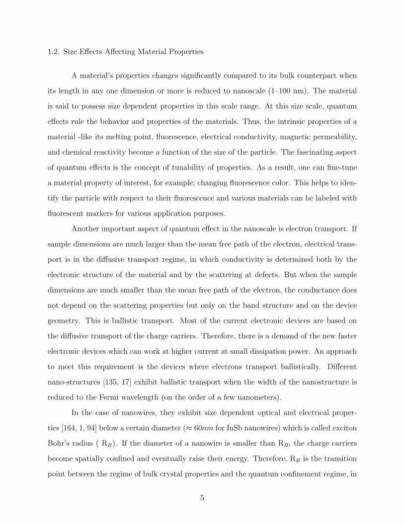
1.2.1. 3- Dimension (3-D) Density of States
Figure 1.2(a) shows density of states in 3-D which possesses the characteristic square
root energy dependence, i.e., the density of states is a continuous function of energy and can
be expressed as:
(1) ρE =(2meff )
3/2E1/2
2π2~3
where ρE is the density of states per unit energy per unit volume.
1.2.2. 2-Dimension (2-D) Density of States
Figure 1.2(b) shows the density of states in 2-D in which the density of states per
unit energy per unit area can be expressed as
(2) ρE =meff
π~2
This density of states in (x, y) accompanies states associated with the value of kz (or nz).
As a result, each kz ( or nz) value is accompanied by a sub-band. Thus we can express this
as
(3) ρE =meff
∑nz
Θ(E − Enz)
π~2
where nz is the index associated with the confinement energy along the z direction and
Θ(E − Enz) is the Heaviside unit step function, defined by
(4) Θ(E − Enz) = 0 ifE < Enzand Θ(E − Enz) = 1 ifE > Enz .
6

Thus, the 2-D density of states remains the same within a sub-band but once the next
sub-band is reached, it increases in a step-wise manner.
1.2.3. 1-Dimention (1-D) Density of States
Figure 1.2(c) shows the density of states in 1-D in which the density of states per
unit energy per unit length is given by the expression
(5) ρE =(2meff )
1/2
π~(E)1/2.
Thus in 1-D the density of states has the characteristic of inverse square root dependence
on energy.
1.2.4. 0-Dimension (0-D) Density of States
Figure 1.2(c) shows the density of states in 0-dimension(0-D). In 0-D, the density of
states is just a series of delta functions so that all three dimensions exhibit carrier confine-
ment:
(6) ρE = 2δ(E − Enx,ny ,nz).
Thus, as a result of the change of energy levels and DOS, nanostructure opens many per-
spectives to engineer the electronic properties of materials.
1.3. Nanowire Growth Techniques
There are three established techniques for the synthesis of nanowires:
(i) Physical vapor deposition,
(ii) Chemical vapor deposition, and
(iii) Electrochemical method.
1.3.1. Physical Vapor Deposition (PVD)
The PVD growth technique requires ultra-high vacuum (of the order of 10−9Torr)
and hence requires highly sophisticated growth equipment like molecular beam epitaxy
(MBE) [134], chemical beam epitaxy (CBE) [82], or thermal evaporation system [89]. In this
7
( a ) ( b )
( c ) ( d )
Figure 1.2. Density of states for (a) 3-D showing E1/2 dependence. (b) 2-D
showing no dependence in energy, i.e., density of states remains same within
a sub-band and increases in a step-wise manner when the next sub-band is
reached. (c) 1-D showing E−1/2 dependence. (d) 0-D showing characteristic
series of delta functions.
technique, source material is evaporated and condensed directly onto the substrate where
no catalyst is required. There are certain advantages of using PVD technique over other
growth techniques; the main advantages being the use of ultra-high vacuum that reduces
contamination/oxidation of material surfaces, the low growth temperature, in situ monitor-
ing of growth and controlled growth rate that prevents inter-diffusion during the fabrication
of hetero-structures.
8

1.3.2. Chemical Vapor Deposition (CVD)
In the CVD growth technique, a precursor gas is delivered to the surface of the
substrate, where the synthesis occurs under catalytic conditions. In this technique, the wafer
(substrate) is exposed to volatile precursors, which react and/or decompose on the substrate
surface to produce the desired deposit. It is one of the most widely used techniques for the
growth of nanowires in which growth of the nanowires happens at ambient pressure or at a
relatively low vacuum compared to the PVD technique.
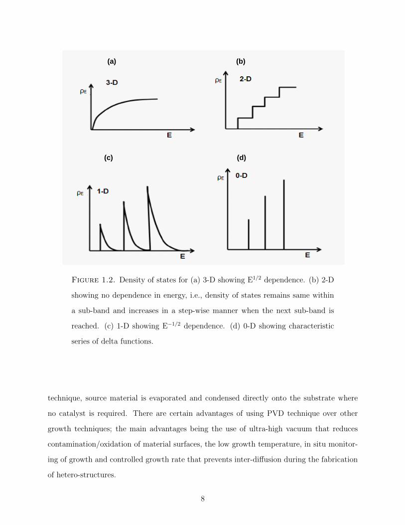
A schematic of the experimental set up of CVD system used for growing InSb, In
and Sb nanowires in this thesis is shown in Figure 1.3. It comprises a resistance–heated
furnace with three temperature-controlled zones. The temperature of the two end zones
can be controlled from the central zone in a master-slave approach. The upper limit of the
temperature in the master zone is 1200C and the slave zones can be set to 200C above or
below the master zone temperature. The positions of the source and growth substrate can
be adjusted according to the requirement of the growth condition for the different nanowires.
Flow of the gas and pressure inside the chamber can be adjusted using a gas flow controller
and pressure flow controller, respectively.
1.3.3. Electrochemical Method
This growth technique is a promising alternative for low temperature synthesis of
nanostructures under ambient conditions. It enables accurate process control through control
of experimental variables like pH and concentration of the electrolyte, applied electrical bias,
and temperature. The schematic of a standard electrochemical cell is shown in Figure 1.4
which consists of three electrodes, one of which functions as the reference electrode and the
other as the working electrode (cathode) and the counter electrode (anode). A Si substrate
coated with gold ( 100 nm) is used as the working electrode whereas a platinum coil is used as
the counter electrode. A DC power supply maintains a constant potential difference between
the electrodes and enables a current to flow during the electrodeposition process.
9
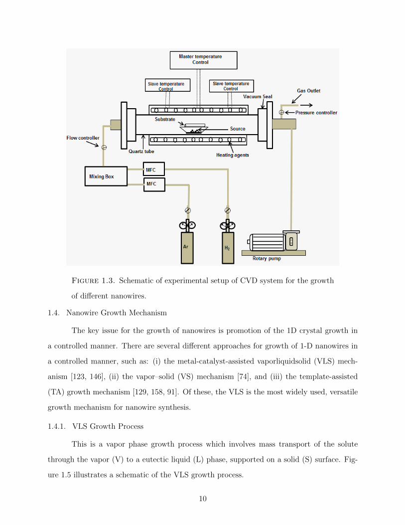
Figure 1.3. Schematic of experimental setup of CVD system for the growth
of different nanowires.
1.4. Nanowire Growth Mechanism
The key issue for the growth of nanowires is promotion of the 1D crystal growth in
a controlled manner. There are several different approaches for growth of 1-D nanowires in
a controlled manner, such as: (i) the metal-catalyst-assisted vaporliquidsolid (VLS) mech-
anism [123, 146], (ii) the vapor–solid (VS) mechanism [74], and (iii) the template-assisted
(TA) growth mechanism [129, 158, 91]. Of these, the VLS is the most widely used, versatile
growth mechanism for nanowire synthesis.
1.4.1. VLS Growth Process
This is a vapor phase growth process which involves mass transport of the solute
through the vapor (V) to a eutectic liquid (L) phase, supported on a solid (S) surface. Fig-
ure 1.5 illustrates a schematic of the VLS growth process.
10

Figure 1.4. Schematic of electrochemical cell.
It involves the absorption of source material from the gas phase into a liquid droplet
of catalyst (a molten particle of catalyst on a silicon substrate), which serves as the seed
promoting nanowire growth. This seed serves as a preferred site for further deposition of
material at the ’liquid–solid’ interface of the liquid droplet. Upon super-saturation of the
liquid alloy, a nucleation event generates a solid precipitate of the source material, promoting
the elongation of the seed into a nanowire. Wagner and Ellis [123] showed that growth of
the nanowire only occurs below the liquid droplet and the nanowire diameter is controlled
by the diameter of the alloy liquid droplet. The nucleated crystals (nanowires) have very
high aspect ratios, owing to the anisotropy of the growth rates for different crystal facets.
As growth proceeds the droplet rides on top of the solid nanowire.
Figure 1.6 shows the binary phase diagram [137] for the AuSi system from which it
11

Figure 1.5. Schematic representation of VLS mechanism.
can be seen that the minimum growth temperature for Si should be higher than the eutectic
point of the system (336C). When the sample is heated above the eutectic temperature,
there occurs the formation of a liquid AuSi alloy, and the composition of the AuSi alloy will
follow the liquidus line (solid line), an equilibrium between the solid and liquid phase. The
composition of the liquid is determined by the amount of supplied Si. Thus, the additional
supply of Si increases the Si concentration in the droplet beyond the equilibrium composition
and renders it into a supersaturated state. This supersaturation state is a thermodynami-
cally unstable state and results the precipitation of the solid phase from the supersaturated
liquid alloy until an equilibrium state is reached. Therefore by continuously supplying Si
from a Si precursor, Si nanowires can be synthesized through this non-equilibrium process.
The diameter of the synthesized nanowire depends on the size of the catalyst droplet, the
12

+ L + L
+
a n d : S o l i d p h a s e s o f A u a n d S i r e s p .
L
Figure 1.6. Phase diagram of the Au-Si system [137].
minimum radius Rmin of which is given by equation (7) [98]:
(7) Rmin = (2Vl)/(RTln(s))σlv
where Vl is the molar volume of the droplet, σlv is the liquidvapor surface energy, and s is the
degree of supersaturation of the vapor. Equation (7) suggests that a smaller size metal-alloy
catalyst droplet requires a higher degree of supersaturation.
But according to the Gibbs–Thompson effect, the chemical potential difference ∆µ
of the component species in the liquid droplet is given by equation (8) [54]:
(8) ∆µ = 4γ/d
where γ and d are the surface energy and the diameter of the droplet, respectively. Thus
equation (8) indicates that the chemical potential of the component species in the metal
13

alloy catalyst becomes high as the size of the catalyst decreases. As a result, it is extremely
difficult to dissolve a vapor component into a liquid catalyst alloy as the size of the droplet
decreases. This eventually prevents the droplet from going into the supersaturated state, an
essential requirement for inducing nanowire growth. Additionally, nanoparticles have strong
attractive van der Waals forces which cause them to agglomerate into larger particles. Also,
nano-sized particles undergo Ostwald ripening at high temperature. As a result, nano-sized
particles tend to transform into large particles to attain a lower energy state at high temper-
ature. Therefore, both the van der Waals attractive forces and Ostwald ripening lead to the
formation of larger diameter droplets resulting in the larger–diameter 1D structures. There-
fore, it is extremely difficult to decrease the size of droplets and, eventually, the diameter
of nanowires in an unlimited manner using the VLS growth mechanism. Thus, care should
be taken during positioning the nano-sized catalyst on the substrate for the growth of very
thin 1D nanostructures.
During VLS growth, one of the factors that determines the growth rate is diameter,
i.e., the larger the nanowire diameter, the faster is its growth rate. This is attributed to
the famous Gibbs–Thomson effect, i.e., the decrease of supersaturation as a function of the
nanowire diameter:
(9) ∆µ = ∆µ0 − 4αΩ/d
where ∆µ (the driving force for nanowire growth) is the difference between the chemical
potentials of the nanowire growth material in the vapor phase and substrate. ∆µ0 is the
limiting value of the difference of chemical potential for the nanowire when d → ∞. Ω is
the molar volume of the catalyst material and α is the specific free energy of the nanowire
surface. Due to the change of the driving force (the chemical potential difference), nanowires
with small diameters grow very slowly compared to thick nanowires which grow faster [41].
At a particular critical diameter where ∆µ = 0, nanowire growth stops completely.
Another factor which decides whether nanowire growth happens or not is the degree of
supersaturation of the catalytic drop with the flux of the growth material, and this depends
14

upon the size of the catalytic drop. If size of the catalytic drop is really big, e.g., ≈ 12µm as
in Figure 1.7(a), it just initiates the growth but does not fully support the actual nanowire
growth as shown in Figure 1.7(b). This is due to insufficient supersaturation of the catalytic
drop. But as the diameter decreases (≈ 8µm), nanowires started to grow as in Figure 1.7(c)
due to the increased degree of supersaturation. Further decreasing the size of the catalyst
(≈ 100 nm) as in Figure 1.7(d), strongly supports the VLS growth mechanism of nanowires,
with a sufficient degree of supersaturation of the catalytic drop.
( a ) ( b )
( c ) ( d )
Figure 1.7. Growth of nanowires with respect to size of the catalyst (a)
≈ 12µm. (b) ≈ 8µm. (c) 100 nm.
1.5. Focus of the Thesis and Layout
The focus of the research in this thesis was synthesis and characterization of the
narrow band gap InSb nanowires and wide band gap In2O3 nanowires and ZnO nanowires
15

and nanotubes, along with the study of their electronic properties. More specifically, the
aims of the study were:
(1) To optimize the growth of InSb nanowires and control their morphology by tuning
parameters such as pressure and temperatures, etc, during growth.
(2) To optimize the route for the growth of metallic (In), semiconducting (InSb) or
semi-metallic nanowires using a chemical vapor deposition system by controlling
temperature and Sb vapor pressure in the higher eutectic region of the InSb phase
diagram.
(3) To synthesize In2O3 nanowires and study their gas sensing behavior.
(4) To establish a successful synthesis route for ZnO nanowires and nanotubes and grow
of transition metal (Fe) doped ZnO nanotubes.
(5) To characterize the morphology, chemical composition, crystal structure and Ra-
man/PL optical spectra of these as-grown 1D nanostructures using electron mi-
croscopy and other microscopes based on laser and X-ray probes.
(6) To study the electron transport in different nanowires and their temperature depen-
dence to investigate their conduction mechanism.
Chapter 2 describes the synthesis process of InSb nanowires using the standard VLS
growth mechanism, in a high temperature chemical vapor deposition (CVD) system. It
also describe the synthesis process of Fe doped ZnO nanowires and nanotubes using a low
temperature electrochemical method. Chapter 3 descibes the effect of growth temperature
on the stoichiometry of InSb nanowires. Results of structural and composition character-
ization are presented, using tools such as the scanning electron microscope (SEM), high
resolution transmission electron microscope (HRTEM) with energy dispersive X-ray spec-
troscopy (EDXS). 2-terminal and 3 terminal transport measurements are also presented in
this chapter for a single stoichiometric Insb nanowire. Chapter 4 discusses defect formation
in InSb nanowires and its effect on stoichiometry and carrier transport. Chapter 5 presents
a discussion of the synthesis of metallic (In), semiconducting (InSb), and semimetallic (Sb)
nanowires through control of indium antimonide growth parameters. It also provides de-
16

tails about the properties of the as-grown crystalline nanowires determined through electron
transport measurements and temperature dependent resistance measurements. Chapter 6
discusses indium oxide nanowire growth and its gas sensing application for oxidising and
redusing gases. Chapter 7 provides the details about growth, structural and optical charac-
terization of Fe doped ZnO nanowires and nanotubes. It also provide information about the
magnetic moment of undoped and Fe doped ZnO nanotubes using a simple method called
the Gouy method. And finally, Chapter 8 summarizes the findings of this work and possible
future projects.
17

CHAPTER 2
SYNTHESIS OF INDIUM ANTIMONIDE NANOWIRES AND IRON DOPED ZINC
OXIDE NANOWIRES AND NANOTUBES
2.1. Synthesis of InSb Nanowires
InSb nanowires that were synthesized in this work were grown by a CVD method in
which source materials are introduced into the gas phase and transported to the substrate
with the flow of carrier gas (e.g. Ar, H2). A chemical reaction takes place in the vicinity
of the heated substrate, leading to the growth of the InSb nanowires. In this thesis, InSb
nanowires were grown on a Si substrate coated with Indium (In) or gold (Au) as a catalyst.
The metal coated substrates were placed face down right above the source material and a
temperature gradient was maintained between the substrate and the source material.
The schematic of the CVD system for the growth of the InSb nanowires is shown
in Figure 1.3 (Chapter 1). It consists of a 1 inch quartz tube housed in a three-zone pro-
grammable temperature controlled furnace (Carbolite Model HZS) with a master temper-
ature control having control over two slave temperature control regions. The three zone
furnace control system is to provide a longer uniform working zone within the furnace. Dur-
ing growth of InSb nanowires, flow of the gas mixture and pressure inside the quartz tube
were adjusted using a gas flow controller and pressure flow controller, respectively. Pure
InSb powder (Alpha Aesar, 99.99 % purity) was used as the source material and placed in
an alumina boat at the center of the quartz tube. Si substrates were cleaned by sonicating
first with acetone and then with alcohol for about 10 minutes, followed by a deionized water
rinse before thermal evaporation of the catalyst seed layer. Then, the Si substrate coated
with a 300 nm thick In film was placed ‘face down’ right above the source using a specially
designed, temperature calibrated sample holder. The source and substrate temperatures
were maintained at ≈ 526C and at ≈ 480C, respectively. The growth chamber was evacu-
ated to 120 Torr and flushed with a high flow of the Ar +H2 gas (flow rate in standard cubic
centimeters per minute (sccm) = 100) for almost 1 hour to eliminate O[2 before heating the
18

system. Then, the furnace was rapidly heated at a rate of 60Cmin−1 to a pre-determined
set point under the constant flow of H2 (100 sccm) and nanowires were grown usually for 1-3
hours under an H2 ambient.
2.1.1. InSb Nanowires Using In as a Catalyst
The details of the schematic of the VLS growth mechanism were discussed in Fig-
ure 1.5 in Chapter 1. It involves the absorption of Sb vapor from an InSb source in gas phase
into a liquid droplet of In (used as a catalyst) to form an InSb alloy droplet. The growth
mechanism is accomplished by the antimonidization of In droplets, where molten In droplets
are supersaturated with Sb to produce InSb nanowires.
Figure 2.1 shows the binary phase diagram of InSb [23] which shows that the growth
of stoichiometric InSb nanowires occurs in a narrow temperature range. Outside this narrow
growth temperature window, the nanowires are either In or Sb rich. At the extreme left of
the phase diagram, there exists a phase consisting of pure In with a melting point of 156C.
At the extreme right of the phase diagram, there exists an elemental Sb phase with a melting
point of 630C. The phase diagram is characterized by the presence of two eutectic points at
0.8 (154C) and 68.2 (493C) at.% Sb with extremely low and orders of higher solubility of
In in Sb, respectively. There is another region in the phase diagram at temperature 493C
where the solubility of Sb is less compared to 68.2 at.%, i.e., an In excess region.
2.1.2. InSb Nanowires Using Au as a Catalyst
The details of the schematic of the VLS growth mechanism were discussed in Fig-
ure 1.5 in Chapter 1. It involves the absorption of InSb vapor from InSb source in gas phase
into a liquid droplet of Au (used as catalyst) to form a Au-InSb alloy droplet. When the
alloy droplet supersaturate with InSb vapor, InSb nanowires precipitate out. The Au droplet
which determines the diameter of the nanowire rides at the top of the nanowire, indicating
the VLS growth mechanism.
Figure 2.2 shows the ternary phase diagram of Au-In-Sb [81] for the growth of stoichio-
metric InSb nanowires.The phase diagram shows the eutectic point of Au-In-Sb at ≈ 323C,
19

Figure 2.1. InSb phase diagram.
forming the liquidus phase beyond this temperature to allow diffusion of elemental In and
Sb in Au (melting point: 1064.43C). Due to the large accommodation coefficient of the
liquid phase (Au-In-Sb alloy droplets), it acts as the most preferred site for the incoming In
and Sb containing vapor phase to initiate nucleation of a InSb nanowire. At the right side of
the phase diagram, there exists an elemental Sb phase with rhombohedral crystal structure
where solubility of In in Sb is really less.
2.1.3. Synthesis of InSb Nanowires in the Presence of Oxygen
Traces of oxygen in the growth chamber during synthesis of InSb nanowires result in
the growth of In2O3 or Sb2O3 nanowires instead of InSb nanowires. If the growth temperature
is≈ 550C or higher and in the presence of O2, it favors the formation of In2O3 nanowires.The
growth procedure was the same as for InSb nanowires but only the difference was in the
20
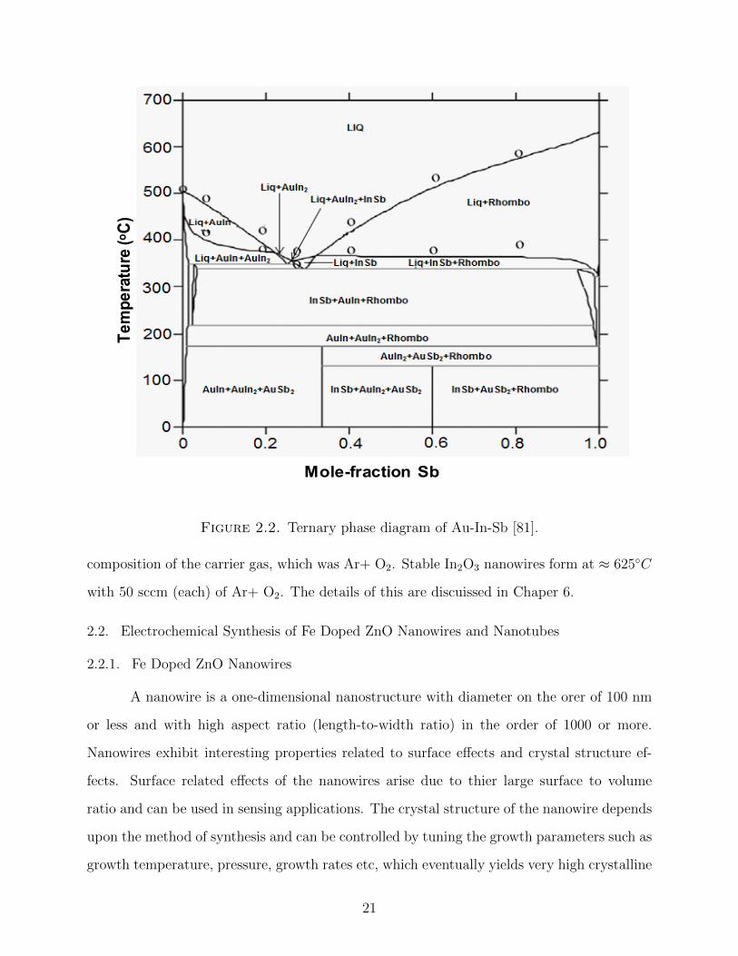
Figure 2.2. Ternary phase diagram of Au-In-Sb [81].
composition of the carrier gas, which was Ar+ O2. Stable In2O3 nanowires form at ≈ 625C
with 50 sccm (each) of Ar+ O2. The details of this are discuissed in Chaper 6.
2.2. Electrochemical Synthesis of Fe Doped ZnO Nanowires and Nanotubes
2.2.1. Fe Doped ZnO Nanowires
A nanowire is a one-dimensional nanostructure with diameter on the orer of 100 nm
or less and with high aspect ratio (length-to-width ratio) in the order of 1000 or more.
Nanowires exhibit interesting properties related to surface effects and crystal structure ef-
fects. Surface related effects of the nanowires arise due to thier large surface to volume
ratio and can be used in sensing applications. The crystal structure of the nanowire depends
upon the method of synthesis and can be controlled by tuning the growth parameters such as
growth temperature, pressure, growth rates etc, which eventually yields very high crystalline
21

quality with fewer defects. Thus, due to their high crystalline quality and the possibility of
producing defect free heterostructures, they are promising candidates for industrial applica-
tion. Bottom-up approach have been used to synthesized nanowires in which they are formed
by self-organized growth, atom by atom in a highly controllable manner. The choice for ZnO
nanowires in this work is due to their promising application in optoelectronic devices [97].
ZnO nanowires have been grown by varieties of techniques such as metal-organic
chemical vapor deposition [69], pulse laser deposition [6] and chemical vapor deposition [49].
These methods provide easy routes for doping and control of growth parameters, but typ-
ically require vacuum systems and high growth temperature of ≈ 800C. Compared to
other methods, electrochemical syntheses is a competitive, low-temperature method for the
growth of high quality ZnO nanowires, and has certain advantages such as easy control the
dimensionality by adjusting electrolyte concentration, simple and low equipment cost, and
speed. Since the growth mechanism of ZnO nanowires and nanotubes is not VLS, no phase
diagram for this growth was discussed.
In electrochemical synthesis, required material is deposited on an electrode by sup-
plying an electric current between two electrodes separated by an electrolyte, and where
reactions essentially takes place at the electrode - electrolyte interface. A schematic of the
electrochemical cell used for the growth of Fe doped ZnO nanowires is shown in Figure 1.4
(Chapter 1).
2.2.2. Fe Doped ZnO Nanotubes
Among different morphologies of nanostructures, nanotubes are considered promising
candidates for varied applications such as dye-sensitized solar cells and sensors with improved
performance and higher sensitivity due to their tubular structure. This tubular structure is
expected to facilitate the confinement effect and high aspect ratio could provide an effective
way to store hydrogen [50].
In this thesis, an electrolyte having a mixture of FeCl3 (0.1mM), ZnCl2 (5mM) and
KCl (0.1M) and an electrolyte having a mixture of FeCl3 (0.1mM), ZnCl2 (6mM) and KCl
(0.2M) were used for the growth of Fe doped ZnO nanowire and nanotubes.The growth of
22

ZnO nanorods occurs by O2 reduction in a solution of ZnCl2 as zinc precursor and KCl as
electrolyte according to the reaction (11) and (12) as follows:
(10) O2 + 2H2O + 4e− → 4OH−
and
(11) Zn2+ + 2OH− → ZnO +H2O
The details of the procedure for the growth of Fe doped ZnO nanowires and nanotubes are
presented in Chapter 7.
2.2.3. Diluted Magnetic Semiconductors (DMS)
DMS are non-magnetic semiconductors doped with a low percentage (< 3%) of tran-
sition metals (TM). They are expected to be easily integrable with existing semiconductors
and also highly spin-polarized. DMS materials have attracted much attention due to their
promising application in spintronics devices, in which one can exploit both the spin and
the charge of the carriers, to understand the fundamental properties of the materials. The
first report on DMS properties of semiconductor alloys like Zn1−x Mnx Te and Cd1−x Mnx
Te appeared in the 1980s. The weak value of ferromagnetism obtained by A.Wasiela et al.
with Curie temperatures ( Tc) of only a few K [29] was completely inadequate for practical
device applications at room temperature (RT). More recently, Mn-doped InAs [45, 48] and
GaAs [47, 133] showed quite promising ferromagnetism at a Tc of 173 K, but still too low
for RT device applications. Therefore, in the continuous search for materials with higher
values of Tc, the report of RT ferromagnetism in the Co doped TiO2 system by Matsumoto
et al. [154, 155] has triggered great interest to investigate this property in other oxide-based
DMS such as TM-doped ZnO [72], SnO2 [120], Cu2O [121] and In1.8 Sn0.2 O3 [62].
Doping in ZnO nanostructure provides a method to adjust the electrical, optical, and
magnetic properties, which is very important for many applications [126] such as sensing,
lasing etc. Differents types of dopants have been used for doping ZnO nanostructure such as
23

Sn, As, S, Cd, FeCo, In, Cu, Mn, and Al [80, 70, 84]. Transition metal iron (Fe) was used as
the dopant for doping ZnO nanowires and nanotubes in this thesis. The effective magnetic
moment found in this work using a magnetic susceptibility balance is strong evidence that
Fe doped ZnO nanotubes have the maximum magnetic moment that an isolated Fe atom
with a d6 electron [124] configuration can have according to Hunds rule. The value of max-
imum magnetic moment in Fe doped ZnO, i.e., Fex Zn1−x O, is due to strong directional
hybridization between O-p and TM-d bands to keep the tetrahedral bonding. Thus, the Fe
doped ZnO nanotubes we describe in this thesis can be a promising DMS for spintronics
device application.
2.3. Size Effect and Quantum Confinement of As-grown Nanowires (ZnO, In2O3 and InSb)
The as-synthesized ZnO and In2O3 nanowires had diameters in the range of 60–80
nm. The RB values of ZnO and In2O3 are 2.34 nm [105] and 2.14 nm [95], respectively.
Therefore, no quantum confinement effects are expected in those nanowires. However, for
InSb nanowires whose diameter are ≈ 40 nm, quantum confinement effects are expected
due to its higher value of RB, i.e., 60 nm. As a result band gap energy becomes diameter
dependent and electron transport is expected to be in the ballastic regime instead of diffusive
regime. But due to high carrier concentration in Insb nanowires (calculated in Chapter 3),
electron transport was found to be in the diffusive regime.
2.3.1. Effect of Quantum Confinement on Band Gap for As-grown InSb Nanowires
For a cylindrical nanowire, electron wavefunctions are described in terms of a cylin-
drical envelope function and perfect crystal Bloch states at the conduction band minimum
(CBM) and valence band maximum (VBM). In the bulk crystal case of a semiconductor, the
only concern is with a single unit cell by assuming that the crystal itself is periodic. But,
in the case of the nanowire, we require the additional constraint that the structure must
take the shape of a cylinder, with the periodic behavior occurring dominantly along the axis
of the cylinder. In a periodic potential, the energy levels are given by energy bands: for
each wavevector k there are several bands En(k) . Near the band edges, at either minima
24

or maxima of the wavevector, the bands have approximately a parabolic dependence on k
and hence the carriers behave as particles with an effective mass. In the envelope function
approximation, the total wave function in the nanowire is written as a product of a slowly-
varying envelope function and the crystal Bloch functions at the band edges, and is given
by [103, 11]
(12) ψkz ,m,n(ρ, φ, z) = CmJmn(kρ)eimφeikzz
where the wave functions along the wire are plane waves with kz wave vector. The radial
part’s of the wave functions are Bessel functions, Jmn, with m = 0,±1,±2, ...... the an-
gular quantum number and n = 1,2,3,....the radial quantum number. The corresponding
eigenenergies are
(13) Ekzmn =~2βmn2m∗R2
+~2k2
z
2m
where βmn are the zeros of the Jmn Bessel function. Therefore, the energy spectrum is given
by parabolic subbands with the bottoms located at the eigenvalues
(14) Emn =~2β2
mn
2m∗R2
which are solutions of the Schrodinger equation perpendicular to the axis. Thus, the energy
of the electron at the conduction band maximum is similar to that of the free electron case,
except that the electron carries an effective mass due to the properties of the semiconductor.
For boundary condition Jmn( where k is perpendicular to R at R = 0, R is the radius of the
nanowire), there would be discrete values of energy of the form Emn for a given m and nth
zero of k.
Unlike the conduction band, the valance band corresponds to a p-type atomic state,
which leads to a 6-fold degeneracy (3-fold degenerate states in the direction of motion and the
rest for spin degeneracy) in total in the valance band. Thus, the degeneracy splits into a 4-fold
state and 2-fold state corresponding to angular momentum J=3/2 and J= 1/2, respectively.
25

By assuming energy levels in the light and heavy holes to be much less than the spin-orbit
coupling energy, one can ignore the split-off holes, leaving a 4-fold degeneracy among the
light and heavy hole states. The basic band structure layout is shown in Figure 2.3.
Figure 2.3. Basic band structure layout in InSb.
Therefore, for InSb nanowires of 40 nm diameter, the energy shift for electrons in
the conduction band using equation (19) with β01 (where β01 =2.405 is the first zero of the
zeroth-order Bessel function) and m∗ = 0.014 m0 ( where m0 = 9.11x (10)−31 kg is the rest
mass of the electron) was calculated to be 39.5 meV. Similarly, the energy shift for holes in
the valance band using equation (19) with m∗ = 0.36 m0 was calculated to be 1.53 meV.
Thus, the total increase in band gap due to confinement in 40 nm diameter InSb nanowire
is 41.03 meV. As a result, the band gap for the InSb nanowire of diameter 40 nm becomes
0.21 eV whcih is 24% more than its bulk value(0.17 eV).
26

CHAPTER 3
INFLUENCE OF GROWTH TEMPERATURE ON THE STOICHIOMETRY OF
INDIUM ANTIMONIDE NANOWIRES1
3.1. Introduction
In recent years, InSb has attracted attention due to the fact that InSb photo-voltaic
detectors can cover a spectral response range equivalent to PbSe and PbS photo-conductive
detectors, but with higher response speed and better signal-to-noise ratio [33, 42, 79]. Syn-
thesis of crystalline InSb as a low-dimensional system coupled with its many advantages could
lead to the realization and development of an entirely new branch of nanoscale optoelectronic
devices. The challenge in growing InSb nanowires is in maintaining the stoichiometry of the
growing crystal. This work showed that stoichiometric InSb nanowires can only be grown in
a narrow range of temperatures, due to the significant partial pressure difference between In
and Sb vapors in contact with the InSb crystal [55].
The purpose of this work is to investigate the stoichiometry of the InSb nanowires as
a function of growth parameters.We have demonstrated the use of two metal catalysts, which
serve as the seed layer for the growth of nanowires by VLS mechanism and the effect of the
choice of this layer on the growth parameters. The growth of stoichiometric InSb nanowires
by the vapor phase transport method occurs in a very narrow temperature window. Outside
this narrow growth temperature window, it was possible to grow nanowires that are In rich
or Sb rich. In rich wires may be synthesized at high temperatures due to loss of Sb, and Sb
rich wires at low temperature due to insufficient supply of In in the vapor phase.
3.2. Experimental Details
InSb nanowires were grown on Si substrates using the vapor assisted VLS growth
mechanism and details of which are explained in Chapter 2.
1This entire chapter is reproduced from U. Philipose, Gopal Sapkota, J. Salfi and Harry E. Ruda,”Influence of growth temperature on the stoichiometry of InSb nanowires grown by vapor phase transport,”Semicond. Sci. Technol., 25, 075004, 2010 with permission from IOP.
27
3.3. Structural Characterization
In order to obtain morphological and crystallographic information, InSb nanowires
grown under different growth conditions were investigated using a scanning electron micro-
scope(SEM: FEI Nova 200 NanoLab), and a high resolution transmission electron microscope
(HRTEM: FEI Tecnai G2 F20 S-Twin 200 kV) equipped with an X-ray energy dispersive
spectrometer (EDX).
3.4. Results and Discussion
This study revealed that the InSb nanowires grown by this technique had lengths of
15–20 µm and diameters in the range of 30–80 nm. But outside the narrow growth temper-
ature range, it was possible to synthesize In rich nanowires or nanowires rich in Sb.
These results suggest a strong correlation between the substrate/source temperature
and the stoichiometry and morphology of the growing InSb crystal. The melting point of
InSb is about 526C. When InSb is evaporated from a single source, the large partial pressure
difference between the constituent elements results in a higher flux of Sb. However, these
Sb molecules will not condense on the Si growth substrate below 480C [92], as its sticking
coefficient is almost zero below this temperature. Above 480C, incident Sb molecules will
condense on the Si substrate. They will react with In on the substrate and initiate nanowire
growth. The AuIn2-InSb pseudo binary section of the Au-In-Sb phase diagram [87] as well
as the In-Sb phase diagram [116] show that it is possible to super-saturate the molten metal
catalyst (Au-In or pure In) droplets with InSb and nucleate an InSb nanowire by the VLS
growth mechanism. The AuIn2-InSb is a pseudo binary eutectic system with ≈ 12% solubil-
ity of InSb in Au In2.
The substrates with the alloyed Au/In seed layer showed no nanostructure growth
for source temperatures below 500C. At a source and substrate temperature of 450C
(substrate placed over source), the substrate was found covered with islands of the Au-In
alloy. When the source and substrate temperature were increased to 520C, and 480C
respectively, the substrate was found to be covered with thick nanowires and a coarse film
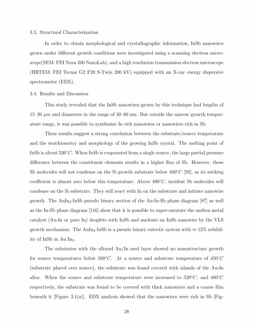
beneath it [Figure 3.1(a)]. EDX analysis showed that the nanowires were rich in Sb [Fig-
28
ure 3.1(b)]and the underlying layer was mostly Au-In [inset of Figure 3.1(b)]. The presence
of the oxygen peak in the EDX spectrum could be attributed to post-growth oxidation of
the Sb nanowires.
Figure 3.1. (a) SEM image of thick Sb rich nanostructures. The substrate
shows a coarse film at the base of the nanostructures. (b) EDX spectrum
confirming that the nanostructures mostly comprise Sb. The presence of an
O peak could signify the oxidation of these nanostructures post-growth. Inset
shows the EDX spectrum confirming the composition of the coarse film to be
mostly Au-In.
The source and substrate temperature were increased to 600C and 510C respec-
tively.The substrate surface was found covered with a high density of nanowires of length
20 µm and diameters ranging from 30 - 60 nm [Figure 3.2(a)]. The nanowires were stoichio-
metric with an In:Sb composition of 1:1, as shown in Figure 3.2(b).
29

Figure 3.2. (a) SEM image of the InSb nanowires. Each wire is over 10 µm
long and has a diameter in the range of 30–60 nm. (b) EDX analysis confirms
the stoichiometric composition of the InSb nanowires.
Figure 3.3 shows the HRTEM image of a single InSb nanowire with the inter-planar
distance between the lattice fringes being 0.67 nm, which is very close to the lattice constant
of 0.648 nm for bulk cubic InSb.
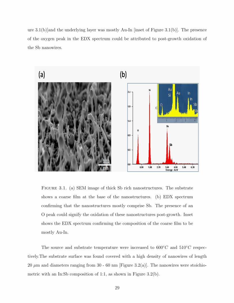
When the source temperature was raised to 650C, with the substrate held at 510C,
nanowires had stoichiometric composition but they appeared tapered and almost conical in
shape as shown in Figure 3.4.
On the other hand, if the source temperature was kept fixed at 600C and the sub-
strate temperature increased above 530C, EDX analysis (see Figure 3.5) demonstrates that
the nanowires are deficient in Sb.
Finally, when the substrate temperature was raised to 600C, it was found the sub-
30

Figure 3.3. HRTEM images of InSb nanowire. The lattice constant is about
0.67 nm and the growth direction is [001].
strate surface to be covered with a high density of nanowires comprised of In. No Sb was
detected along the length of the nanowire, as shown in Figure 3.6(a). The In nanowires
showed no evidence of any structural defects. After removal of these nanowires from the
growth chamber and exposure to the atmosphere, they get quickly oxidized. An HRTEM
image of a single oxidized In nanowire is shown in Figure 3.6(b). An amorphous oxide shell of
approximately 3-5 nm thickness is clearly visible in the HRTEM image. Surface passivation
will be necessary to prevent the oxidation of the nanowire surface. This investigation showed
that the stoichiometric and non-stoichiometric nanowires grow along the [0 0 1] direction.
A summary of the experimental findings, using Au-In as the metal catalyst, is shown
in Table 3.1.
For the case of substrates of Si with a pure In film as the seed layer, growth of InSb
31
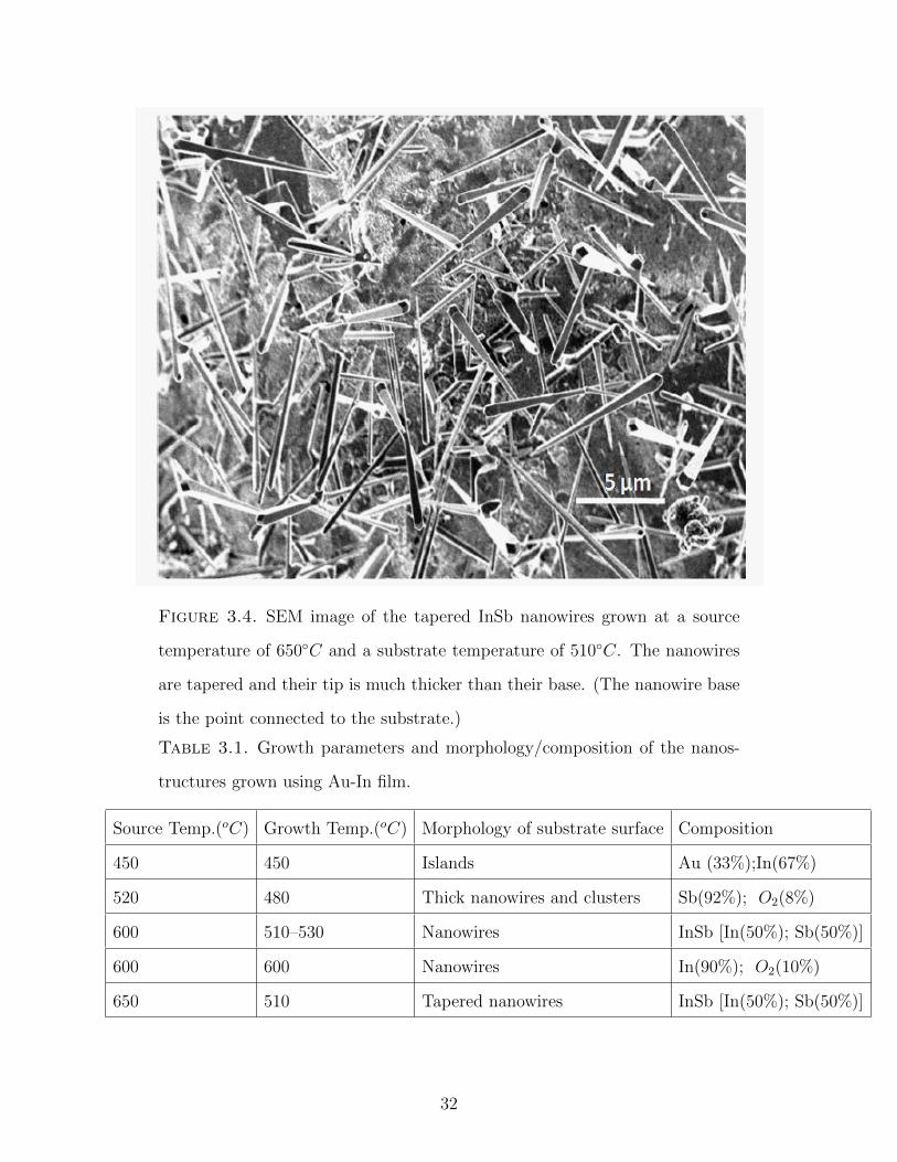
Figure 3.4. SEM image of the tapered InSb nanowires grown at a source
temperature of 650C and a substrate temperature of 510C. The nanowires
are tapered and their tip is much thicker than their base. (The nanowire base
is the point connected to the substrate.)
Table 3.1. Growth parameters and morphology/composition of the nanos-
tructures grown using Au-In film.
Source Temp.(oC) Growth Temp.(oC) Morphology of substrate surface Composition
450 450 Islands Au (33%);In(67%)
520 480 Thick nanowires and clusters Sb(92%); O2(8%)
600 510–530 Nanowires InSb [In(50%); Sb(50%)]
600 600 Nanowires In(90%); O2(10%)
650 510 Tapered nanowires InSb [In(50%); Sb(50%)]
32

Figure 3.5. EDX spectrum of InSb nanowires grown at 530C. The
nanowires have a lower concentration of Sb and are rich in In.
occurred due to antimonidization of In droplets. The optimum growth temperature for sto-
ichiometric InSb nanowires was in the range of 480− 520C, with the source held at 600C.
Above 520C, the InSb nanowires became In rich with loss of Sb, and at a growth temper-
ature of 580C there was a high density of In nanowires, which were quickly oxidized after
exposure to the atmosphere. Nanowires grown using In as the metal catalyst did not show
any evidence of a metal alloy tip, but those grown using AuIn2 as the seed layer showed an
alloyed tip at the end of each nanowire.In the former case, the metal In is consumed during
the growth process in which antimonidization of In droplets leads to the growth of InSb
nanowires. Any In present at the tip cannot be distinguished from the rest of the nanowire.
The region of the phase diagram in which nanowire growth by the VLS mechanism
occurs depends on several growth parameters such as flow rate of precursors as well as tem-
33
( a ) ( b )
Figure 3.6. (a) EDX spectrum of In nanowires grown at 600C. The spec-
trum shows no evidence of any Sb. (b) HRTEM image of the In nanowires
confirming their crystalline nature.
perature and pressure in the growth chamber. In references [107, 108, 28], InSb nanowire
heterostructures were grown by MOVPE at a lower temperature range of 420C - 460C; but
the chamber pressure in these cases were in the mbar range. Moreover, MOVPE also allows
pressure control of the metal-organic precursors thus enabling component flux variation on
the sample during growth. Hence the lower growth temperature could be attributed to the
lower growth pressure and the controlled flow of fluxes to the alloy droplet. In this work, the
nanowires were grown in a reducing environment at atmospheric pressure. Growth tempera-
tures of this work are comparable to those reported by Qi Laura Ye et al., [112] under similar
growth conditions. The fact that nanowires did not grow at substrate temperatures below
500C for substrates coated with Au-In, could be explained by the fact that the Au In2–InSb
34

phase diagram [87] has a eutectic temperature of about 472C. For temperatures below the
eutectic point, InSb is not miscible in the alloyed droplet, preventing nanowire growth by
VLS. As the substrate temperature increases to about 480C, with the source at 520C, there
is a higher concentration of Sb in the vapor flux due to incongruent sublimation of InSb.
Hence, the Au-In-Sb alloy droplet gets quickly saturated with Sb and it precipitates out of
the liquid alloy, producing Sb rich nanowires. As the source and substrate temperature in-
creased to 600C and 510C respectively, the concentration of In in the molten alloy droplet
increases and the result is a stoichiometric InSb nanowire. These stoichiometric nanowires
are thread-like and grow uncontrolled in a ‘weed-like’ manner with no preferred orientation.
The growth window of these stoichiometric nanowires was found to be extremely small, in
the range of 510C – 530C. Increasing the substrate temperature by 50 oC, was found to
reduce the concentration of Sb in the nanowire and at a substrate temperature of 600C,
the nanowire comprise In with no Sb detected along the nanowire length. This is attributed
to the re-evaporation of Sb from the growing crystal on account of its higher vapor pressure.
The In nanowires were about 20 µm long and had very small diameters, in the range of 10 –
30 nm. At higher source temperatures, the nanowires maintained their stoichiometry. How-
ever, they appeared tapered and this could be attributed to lateral growth on the side walls
of the growing nanowire. The inverted cone like structure of the nanowire implies that the
growing tip of the nanowire, which was exposed to the incoming vapor flux was the region
promoting lateral growth.
3.5. Electron Transport Measurements
InSb nanowires grown using parameters chosen to produce stoichiometric composition
(In:Sb = 1:1) were transferred onto degenerately doped Si substrates covered with 100 nm
of SiO2. The locations of several nanowires were identified with respect to pre-patterned
markers, and electron beam lithography was used to pattern four multilayer Nickel (15 nm)/
Gold (150 nm) ohmic contacts per nanowire. After lithography but prior to evaporation
of metallic contacts, samples were dipped in diluted ammonium sulfide (0.3 % by wt. in
deionized water) for 2 minutes to remove the native oxide layer and passivate dangling
35
bonds on the nanowire surface. This step is necessary to produce low resistance contacts.
After wirebonding the samples onto chip carriers, the chips were transferred into a closed
cycle cryostat for electrical measurements.
The current–voltage characteristics of InSb nanowires (stoichiometric nanowires with
In:Sb = 1:1) were obtained by biasing the two outer terminals with a programmable voltage
Va between -100 and 100 mV, and measuring the current I through the nanowire as well
as the voltage V across the two inner terminals. The measured current I is linear with
respect to applied voltage Va as well as the measured voltage V over the full temperature
range T=294 K to T=15 K, and only decreases modestly as temperature decreases. The
dependence of I on Va and V for a typical nanowire with a radius R= 42 nm (measured by
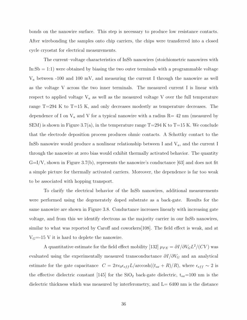
SEM) is shown in Figure 3.7(a), in the temperature range T=294 K to T=15 K. We conclude
that the electrode deposition process produces ohmic contacts. A Schottky contact to the
InSb nanowire would produce a nonlinear relationship between I and Va, and the current I
through the nanowire at zero bias would exhibit thermally activated behavior. The quantity
G=I/V, shown in Figure 3.7(b), represents the nanowire’s conductance [63] and does not fit
a simple picture for thermally activated carriers. Moreover, the dependence is far too weak
to be associated with hopping transport.
To clarify the electrical behavior of the InSb nanowires, additional measurements
were performed using the degenerately doped substrate as a back-gate. Results for the
same nanowire are shown in Figure 3.8. Conductance increases linearly with increasing gate
voltage, and from this we identify electrons as the majority carrier in our InSb nanowires,
similar to what was reported by Caroff and coworkers[108]. The field effect is weak, and at
VG=-15 V it is hard to deplete the nanowire.
A quantitative estimate for the field effect mobility [132] µFE = ∂I/∂VGL2/(CV ) was
evaluated using the experimentally measured transconductance ∂I/∂VG and an analytical
estimate for the gate capacitance C = 2πε0εeffL/arccosh((tox + R)/R), where εeff ∼ 2 is
the effective dielectric constant [145] for the SiO2 back-gate dielectric, tox=100 nm is the
dielectric thickness which was measured by interferometry, and L= 6400 nm is the distance
36
Figure 3.7. (a) Dependence of measured current I on applied voltage Va be-
tween outer terminals and and measured voltage between inner two terminals
V of InSb nanowire for temperatures between 294 K and 15 K, and (inset)
schematic of four terminals on nanowire with labeled potentials and current.
The distance between adjacent electrodes is L= 6400 nm. (b) Dependence of
conductance G=I/V on temperature.
between the two inner contacts. The weak gating translates into a field effect mobility of
∼ 20 cm2V−1s−1 and also results in a very large extrapolated threshold voltage of ∼ −150 V.
The inferred field effect mobility of electrons in the InSb nanowires is more than 3 orders of
magnitude smaller than the drift mobility µ ∼ 77, 000 cm2V−1s−1 of bulk InSb. The electron
concentration in the nanowires can be estimated using n0 = C|VT |/(qπR2L) ∼ 1019 cm−3,
where q is the electronic charge and VT is the threshold voltage. The physical location of
the impurities which contribute these charges could be either on the nanowire surface or
37

Figure 3.8. Dependence of InSb nanowire conductance on back-gate volt-
age. Conductance increases with increasing gate voltage implying electrons
are majority carriers. Only a relatively small change in conductance (approx
10%) can be realized by applying a strong (-15 V) gate bias. Extrapolated
electron concentration is of the order of 1019 cm−3.
inside the nanowire. Due to the large Bohr radius, RB=60 nm, of shallow donors in InSb,
impurity band formation occurs at a correspondingly lower than usual impurity concentration
of approximately nc ∼ (1/RB)3 ∼ 1016 cm−3 which is much less than the inferred impurity
concentration of our InSb nanowires. One plausible explanation for the low electron mobility
is that conduction is taking place by an impurity band. Unlike the InAs surface which has
a high mobility surface electron gas[160], unmodified InSb surfaces do not normally exhibit
n-type conduction[110] and must be modified by, e.g., sub-monolayer evaporation of Cs or
Ag[115] atoms to form a surface electron gas.
38
3.6. Conclusion
The two critical parameters in the growth of crystalline, stoichiometric InSb nanowires
are the source and substrate temperatures. The source temperature controls the evaporation
rates of In and Sb.There is a large difference in vapor pressures between In and Sb and so
when InSb is evaporated from a single source,the Sb molecules are evaporated at first. At a
given source temperature and in a critical substrate temperature range, the evaporated Sb
molecules react with the In atoms and nucleation and growth of crystalline InSb nanowire
begins. The substrate (growth) temperature controls the stoichiometry of the growing crys-
tal. At lower source and substrate temperatures, due to incongruent InSb sublimation, the
nanowires are Sb rich. When the substrate temperature is increased, the re-evaporation of Sb
from the InSb nanowires increases and the nanowires are rich in In. At a growth temperature
of 600C, the nanowires comprise only In with no traces of Sb. Transport measurements on
a single stoichiometric InSb nanowire show that electrons are the majority carriers with a
carrier concentration of ∼ 1019 cm−3.
39

CHAPTER 4
DEFECT FORMATION IN INDIUM ANTIMONIDE NANOWIRES AND ITS EFFECT
ON STOICHIOMETRY AND CARRIER TRANSPORT1
4.1. Introduction
Compound semiconductors have complex defect configurations involving vacancies,
interstitials and antisite defects that influence their electronic and optical properties. Since
high defect concentrations and their charged states can alter the energy band structure of
the semiconductor, there is a need to investigate their type and formation process. There
are several studies on defects in bulk GaAs [88] and InP [117] but very few on InAs and
InSb. The studies on native defects in bulk InSb crystals [10, 75] involve vacancies in In and
Sb sub-lattices. Hoglund et al [3] used the density-functional theory to determine the basic
properties and calculate the formation energies of point defects in InSb with a comparison of
the relative stability of surface and bulk defects. This work showed that the concentration of
defects is considerably larger at the surface compared to the bulk and in some cases defects
tend to segregate to the surface, given sufficient time. Since nanowires have large surface
to volume ratios, a study of the defect forming mechanism as a result of specific nanowire
growth conditions is warranted to facilitate the synthesis of defect free stoichiometric InSb
nanowires.
In this work, a thermodynamic model was developed to show that the occurrence
of native defects in InSb nanowires were influenced by the nanowire growth kinetics and
thermodynamics of defect formation. Optimization of growth parameters for the synthesis of
InSb nanowires is critical, and there are reports of stoichiometry dependence on temperature,
choice of metal catalyst and V/III gas flux ratio [108, 107, 28]. The vapor-liquid-solid (VLS)
growth of nanowires can be initiated either via self catalysis using In or Sb as nucleating seeds,
or by using an alloyed metal catalyst of Au-In. The nanowires used in this study were grown
1This entire chapter is reproduced from U. Philipose, Gopal Sapkota, ”Defect formation in InSb nanowiresand its effect on stoichiometry and carrier transport,” J. Nanopart. Res, 15, 2129, 2013 with permissionfrom Springer.
40

by Chemical Vapor Deposition (CVD) using a thin film of In as the seed layer [53, 112, 136].
The growth of stoichiometric InSb nanowires occurs in a narrow temperature range and
outside this narrow growth temperature window, the nanowires are either In or Sb rich;
the deviation from stoichiometry resulting in high concentrations of vacancy defects in the
nanowires. A direct consequence of these defects affecting the electronic behavior of these
nanowires was reported in chapter 3 [136], with observation of n-type conduction in nearly
stoichiometric InSb nanowires, persisting from room temperature to 15 K and an estimated
carrier concentration of ≈ 1019cm−3.
The objective of this work is to review the thermodynamics of vacancy defects in
InSb and to develop a model showing the dependence of the defect concentration on the Sb
partial pressure. The defect model is validated by examining the nanowire stoichiometry
as a function of growth temperature and Sb partial pressure. This work follows a series of
reports experimentally confirming the presence of In and Sb vacancies in InSb crystal [10, 75,
13]. Hence the thermodynamic model under study in this work considers antimony mono-
vacancies [VxSb], indium mono-vacancies [Vx
In] and charged versions of these two defects,
namely V−In and V+Sb. Interstitial defects are not included in this analysis, primarily because
most of the experimental results of defects in InSb can be interpreted using vacancies as the
dominant defect species. However, the possibility that there could be a high concentration of
interstitial defects cannot be ruled out and as more experimental evidence becomes available
verifying the role of interstitials, the model can be suitably modified.
4.2. Experimental Details
The effect of temperature and hence partial pressure of antimony (P1/2Sb2
) on InSb
nanowire stoichiometry was studied by growing InSb nanowires on Si substrates under dif-
ferent growth conditions, using the vapor assisted vapor liquid solid (VLS) growth mecha-
nism [53, 122, 112, 136] and detailes of which were described in Chapter 3.
4.3. Structural Characterization
In order to obtain morphological and crystallographic information, InSb nanowires
grown under different growth conditions were investigated using a scanning electron mi-
41
croscope (SEM: Hitachi SU1510), and a high resolution transmission electron microscope
(HRTEM: FEI Tecnai G2 F20 S-Twin 200 kV) equipped with an X-ray energy dispersive
spectrometer (EDX). The nanowires were several microns long and had diameters in the
range of 40–80 nm. The nanowire stoichiometry was found to be significantly influenced by
growth temperature.
4.4. Defect Analysis
The growth of InSb nanowires occurs by the VLS growth mechanism and can be
expressed by the reaction:
(15) InSb(s) = In(v) +1
2Sb2(v)
This growth is driven by the chemical potential gradients among vapor, liquid and
solid phases with growth taking place through a mass transfer across the liquid-solid inter-
face. The system of nanowires is characterized by a temperature T at which there are a
certain number of intrinsic point defects in the crystalline nanowires. A reaction equation is
written for the formation of each type of defect in the solid phase and for the formation of
electrons and holes. Each reaction is represented by a mass action condition which applies at
equilibrium. We assume that the conditions are ideal and the mass-action relations can be
expressed in terms of defect concentrations. The mass action equations and the equation of
neutrality are used to determine the defect concentrations in terms of the partial pressure of
Sb2 in the gas phase. The concentration of In and Sb vacancies, [VIn] and [VSb], respectively,
were estimated from [10, 75, 13]:
(16) [V ] = NsitesNconfig exp
(S
k
)exp
(−EfkT
)
where, S is the entropy, Ef is the formation energy of the defect, Nsites is the number of
sites in the lattice (per unit volume) where the defect can be incorporated, k is Boltzmann’s
constant, T is the absolute temperature and Nconfig is the number of equivalent configurations
42

Table 4.1. Equilibrium constants derived from reaction equations.
Reaction equations leading to the for-
mation of vacancies in InSb
Equations for equilibrium constants
based on mass-action relation
In(v) + 12(Sb2)(v) = InSb(s) Kf = PInP
1/2Sb2
12(Sb2)(v) = SbxSb + V x
In Kv =[V x
In]
P1/2Sb2
0 = V xIn + V x
Sb Kxs = [V x
In][V xSb]
V xSb = V +
Sb + e− Kd =[V +
Sb][e−]
[V xSb]
V xIn = V −In + h+ Ka =
[V −In][h+]
[V xIn]
0 = n + p Ki = np
in which the defect can be incorporated. For vacancy defects [21], Nconfig =1. The entropy
and the formation energy of a given defect are based on data reported by Morozov et al., [10].
A review of the native point defects in III–V semiconductors like InSb was recently presented
in a review article by Hurle [56]. The vacancy formation reactions and the corresponding
mass-action relations are given in Table 4.1. The superscript ‘x’ indicates neutral species,
while the superscript ‘+’ and ‘-’ indicates positive and negative species respectively. The
concentrations of free electrons and holes are indicated by n and p and in reaction equations,
free electrons and holes are indicated by e− and ho, respectively.
The electrical neutrality condition is written as [26]:
(17) n+ [V −In] = p+ [V +Sb].
The partial pressures of In (PIn) and of Sb2 (P1/2Sb2
) in the vapor phase are governed by the
equation:
(18) PInP1/2Sb2
= Kf
43

where Kf [in units of (atm)3/2] is the equilibrium constant for sublimation of InSb, which
is a constant at a given temperature and is given by the equation [166]:
(19) Kf = 4.37× 10¹⁰exp(−3.97/kT )
During growth, the compound InSb source provides a minimum total pressure Pmin over the
growing nanowire in the growth chamber, ensuring that it remained an equilibrium InSb
solid phase. The required minimum partial pressure of Sb, (P1/2Sb2
)min is calculated using the
approximation [43]:
(20) (P1/2Sb2
)min ≈ (Kf/2)1/3
The variation of (P1/2Sb2
)min with temperature (within the range of temperatures used
in this work) is shown in the inset of Figure 4.1. At a source temperature of 526C, cor-
responding to the formation of stoichiometric InSb in the In-Sb phase diagram [116, 24],
(P1/2Sb2
)min is estimated to be ≈ 1.2 × 10⁻⁵ atm1/2 (equations 19 and 20). The equations in
Table 4.1 are modified and expressed in terms of the equilibrium constants, to calculate the
concentration of the defects [V−In], [VxIn], [V+
Sb], [VxSb], as a function of (P
1/2Sb2
). Based on the
electrical neutrality conditions of equation 17, a set of four neutrality conditions are estab-
lished: n = [V+Sb]; n = p; [Vx
In] = [V+Sb] and p = [V−In]. The solutions of equations shown in
Table 4.1 for each of these neutrality conditions are then obtained and the evolution chart
of the defects and the possible transitions with increasing Sb vapor pressure for a growth
temperature of 526C is determined. The approximate solution of the set of equations in
Table 4.1 plotted against (P1/2Sb2
) is shown in Figure 4.1.
The approximation implies that in the ranges of (P1/2Sb2
) pressure variation, three defect
regimes ( n = [V+Sb], [V−In]= [V+
Sb], and p = [V−In]) are considered. At low values of (P1/2Sb2
), the
approximation n = [V+Sb] is valid. The concentration of [V−In], and [Vx
In] increases with (P1/2Sb2
)
and eventually its concentration dominates causing a transition to [V−In]= [V+Sb]. As (P
1/2Sb2
)
increases, p also increases and finally at sufficiently high values of (P1/2Sb2
), p = [V−In] will take
44

Figure 4.1. Vacancy defect concentrations in InSb nanowires, determined as
a function of (P1/2Sb2
).
over. Figure 4.2 represents the quantities∑VSb = [V +
Sb] + [V xSb] and
∑VIn = [V −In] + [V x
In] as
a function of (P1/2Sb2
).
It can be seen that nanowires grown under stoichiometric conditions, close to (P1/2Sb2
)min
have a net vacancy concentration of the order of 1018 cm−3. The magnitude of the defect con-
centrations determined by this model are sensitive to the values of equilibrium constants used
for each of the reaction equations. However, the estimated values are in agreement with de-
fect concentrations reported by Morozov et al., [10] and Kendall et al., [75]. These values are
also comparable to measured values of carrier concentrations in InSb nanowires [22, 64, 130],
which were shown to have n-type conductivity and where the carriers were attributed to the
presence of Sb vacancies. The Sb vacancy concentration increases as P1/2Sb2
decreases. It is
therefore essential to maintain an overpressure of Sb-rich vapor for the growth of stoichio-
45

Figure 4.2. Sum of defect concentration (∑V Sb and
∑V Sb) variation with (P
1/2Sb2
).
metric InSb nanowires.
4.5. Results and Discussion
Figure 4.3 is an SEM image of high density of 40–80 nm thick InSb nanowires that
grow from tiny protrusions on sub-micron sized In droplets. The growth of InSb nanowires is
explained on the basis of a spontaneous nucleation mechanism [44, 24], where Sb is supplied
to molten In droplets (of sizes varying from tens of nm to hundreds of nm) by heating a
source of InSb, resulting in the formation of a binary solution containing In and Sb. The
low solubility of Sb in In results in the formation of supersaturated droplets that function
as nucleating seeds for the growth of InSb nanowires. There exists a critical seed size that
promotes nucleation, and nanowire growth occurs by precipitating In and Sb onto these seeds
at the nucleus-liquid interface, as shown in Figure 4.3.
46
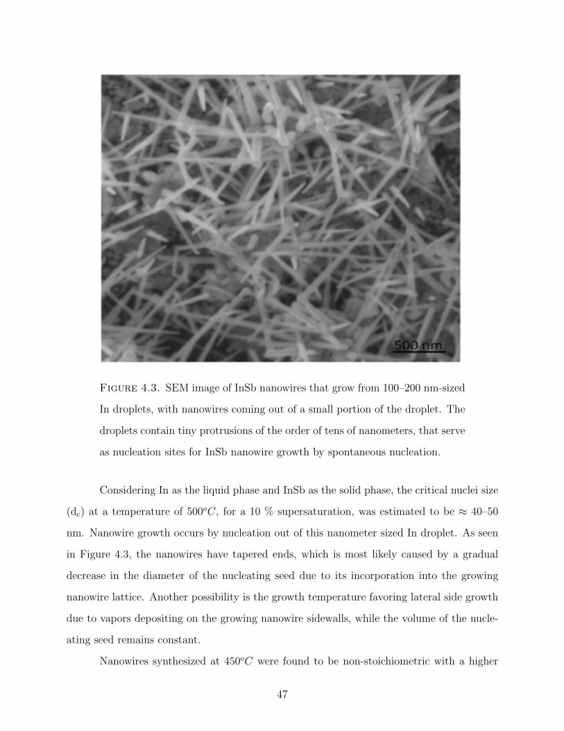
Figure 4.3. SEM image of InSb nanowires that grow from 100–200 nm-sized
In droplets, with nanowires coming out of a small portion of the droplet. The
droplets contain tiny protrusions of the order of tens of nanometers, that serve
as nucleation sites for InSb nanowire growth by spontaneous nucleation.
Considering In as the liquid phase and InSb as the solid phase, the critical nuclei size
(dc) at a temperature of 500oC, for a 10 % supersaturation, was estimated to be ≈ 40–50
nm. Nanowire growth occurs by nucleation out of this nanometer sized In droplet. As seen
in Figure 4.3, the nanowires have tapered ends, which is most likely caused by a gradual
decrease in the diameter of the nucleating seed due to its incorporation into the growing
nanowire lattice. Another possibility is the growth temperature favoring lateral side growth
due to vapors depositing on the growing nanowire sidewalls, while the volume of the nucle-
ating seed remains constant.
Nanowires synthesized at 450oC were found to be non-stoichiometric with a higher
47

concentration of In as compared to Sb. Figure 4.4(a) shows the elemental mapping for a
single In rich InSb nanowire. EDX spectrum (Figure 4.4(b)) confirms the nanowire stoi-
chiometry to favor In with an In:Sb composition ratio of 60:40 at%.
Figure 4.4. (a) SEM image of a 40 nm thick InSb nanowire grown at 450C,
and corresponding elemental maps of In (red) and Sb (green) content in the
nanowire. (b) EDX spectrum of the InSb nanowire with a composition ratio
of 60 at% In:40 at% Sb.
This lack in stoichiometry can be explained on the basis of the defect model (Fig-
ure 4.1 and Figure 4.2). At a growth temperature of 450oC, (source temperature is about
500oC) (P1/2Sb2
)min is ≈ 6 × 10⁻⁶ atm1/2 and the Sb vacancy concentration is of the order of
1019 cm−3. The low Sb2 partial pressure thus accounts for the lack of stoichimetry in InSb
nanowires grown at this temperature.
The InSb nanowire stoichiometry was improved by raising the growth temperature to
48

526oC. Figure 4.5 shows elemental line scans recorded across a 50 nm thick nanowire (from
point A to B, both A and B lying away from the edge of the nanowire). Composition across
the nanowire is uniform with near-stoichiometric ratio of In and Sb. At this temperature,
(P1/2Sb2
)min is estimated to be of the order of 10−5 atm1/2, and from Figure 4.1 and Figure 4.2,
in this region V−In = V+Sb and the net vacancy concentration is independent of Sb partial
pressure and hence appears as a horizontal line.
Figure 4.5. SEM image and elemental mapping showing the stoichiometry
of an InSb nanowire grown at 526C. The line scan extending beyond the
nanowire dimensions and the corresponding EDX spectrum confirms the stoi-
chiometric composition.
indent Figure 4.6 shows the HRTEM image of a single InSb nanowire with the inter-planar
distance between the lattice fringes being 0.67 nm, comparable to to the lattice constant of
0.648 nm for bulk cubic InSb.
49

Figure 4.6. HRTEM image of a single InSb nanowire, with a lattice constant
of about 0.67 nm.
When the growth temperature was raised to 600C, the nanowires comprised of only
In, as shown in the EDX spectrum obtained from these nanowires (Figure 4.7 (a)). The
nanowires were over 20 µm long and had diameters ranging from 30–60 nm, as shown in
the inset. At high temperatures, both the InSb source and the InSb growing crystal lose
Sb, which is swept out of the growth furnace by the carrier gases and this accounts for the
metallic composition of the nanowires at high temperatures. The crystal structure of a single
In nanowire (diameter 50 nm) was investigated using HRTEM and the image of Figure 4.7(b)
shows an inter-planar spacing of about 0.48 nm, comparable to the lattice constant of 0.49
nm for bulk tetragonal In.
These results show that the stoichiometry of InSb nanowires grown by antimonidiza-
tion of In droplets is critically dependent on the growth temperature, with stoichiometric
50

Figure 4.7. (a) SEM image and elemental map of a single 50 nm thick In
nanowire. (b) EDX spectrum obtained from the In nanowire, confirming the
metallic composition of the nanowire. (c) HRTEM image confirming the crys-
talline nature of the 50 nm thick In nanowire with a lattice constant of 0.48
nm.
growth occuring in a very narrow temperature region. The defect model (Figure 4.1) pre-
dicts that the dominant defect species for nanowires grown under stoichiometric conditions
are V−In and V+Sb. The coulomb attraction between these two charged defects suggests that
they are likely to occur as a vacancy pair, a fact that has been confirmed through diffusion
studies for vacancies of In and Sb in InSb [75]. Further studies are required to determine if
the mobility of these vacancy defects could affect the defect concentration as the temperature
is lowered to room temperature.
51

4.6. Electron Transport Measurements
To correlate defect concentration to carrier concentration and to study electron trans-
port in InSb nanowires, two and three-termial transport measurements were made by con-
tacting a single InSb nanowire on a p+ Si substrate covered with a 200 nm thick SiO2 layer.
Metal (Au) source and drain electrodes were fabricated on top of the nanowire. For the
3-terminal measurements, the highly-doped p+ Si-substrate served as the back-gate with a
gate dielectric thickness of 200 nm. Transport measurements were made using Agilent Tech-
nologies B1500A semiconductor device analyzer for determination of carrier concentration
in the nanowires.
Figure 4.8 is a plot of drain current vs. source-drain voltage (Ids–Vds), measured at
room temperature for a single InSb nanowire, grown at 526oC. The contacts were annealed
at 250C in an inert environment to ensure ohmic contacts to the nanowire. Inset of Fig-
ure 4.8 shows the variation in drain current at fixed Vds = 0.2 V, for various gate voltages
ranging from 0 to +10 V.
The current and hence the nanowire conductance was found to increase with increas-
ing gate voltage, attesting to the n-type behavior of the InSb nanowire. The gating is weak
which implies that there is a high electron concentration and only a weak modulation of the
nanowire conductance could be achieved with the applied back-gate voltage. The threshold
voltage VT , which is the gate voltage at which there is a complete suppression of the drain
current, was extrapolated to be -40 V. The electron concentration in the InSb nanowire was
estimated using n0 = C|VT |/(qπR2L) ≈ 2.7 × 1018 cm−3, where q is the electronic charge.
The gate capacitance was estimated from the equation [145]:
(21) C =2πε0εeffL
cosh−1(tox+RR
)where εeff ≈ 2.2 is the effective dielectric constant for the SiO2 back-gate dielectric, tox =
200 nm is the dielectric thickness, R = 25 nm is the nanowire radius, and L = 10 µm is the
distance between the two inner contacts. The value of n0 is comparable to earlier reported
values [156, 22, 51], but is higher than the limit of 1017 cm−3 required for the formation of a
52

Figure 4.8. Variation of drain-source current (Ids) with drain-source voltage (
Vds) at zero gate bias for a single InSb nanowire. The source and drain contacts
to the nanowire were annealed to ensure ohmic contacts to the nanowire. Inset
shows the variation in drain-source current (Ids) with positive gate bias, at Vds
= 200 mV. Ids increases with positive gate bias, attesting to the n-type behavior
of the as-grown InSb nanowires.
degenerate electron system in InSb. Hence the synthesized nanowires are degenerate with the
Fermi level located above the conduction band minimum. The high carrier concentration
has been ascribed to the presence of Sb vacancies in InSb nanowires [22]. The value of
n0 is an order of magnitude lower than our earlier reported value [136], and is attributed
to better control of Sb vapor pressure during the nanowire growth. The experimentally
measured carrier concentration of the order of 1018 cm−3 compares favorably with the vacancy
concentration determined by the defect model, where nanowires grown under stoichiometric
53
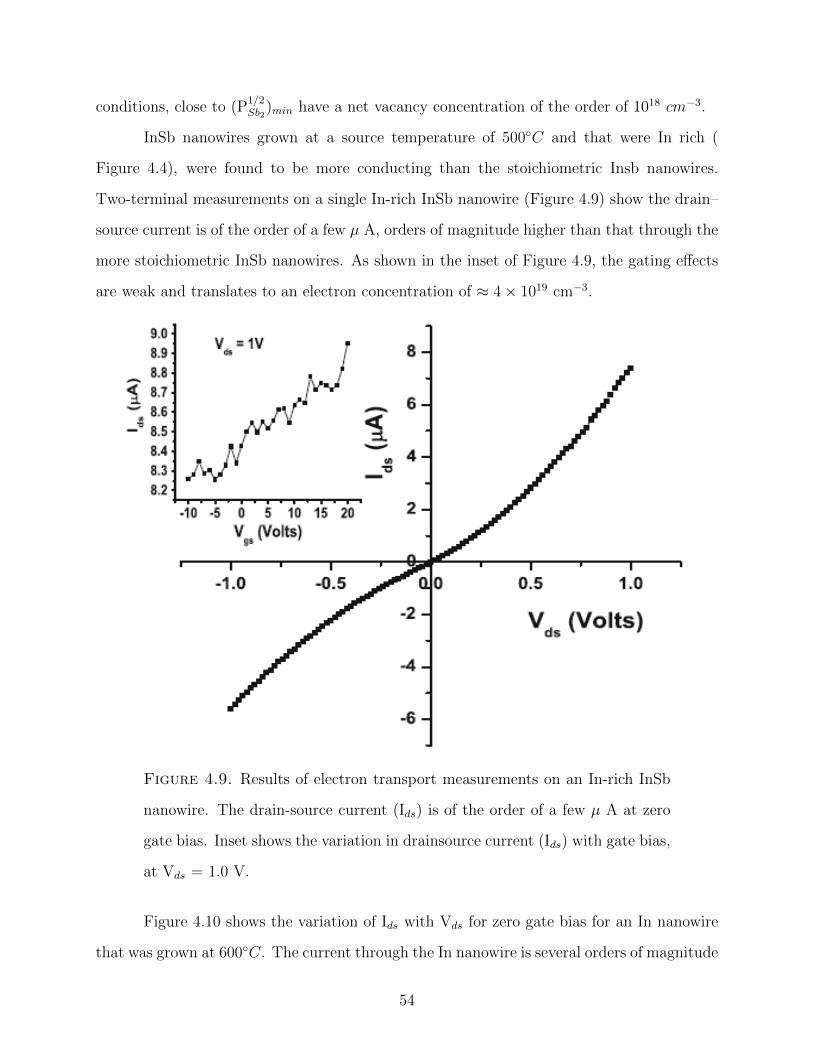
conditions, close to (P1/2Sb2
)min have a net vacancy concentration of the order of 1018 cm−3.
InSb nanowires grown at a source temperature of 500C and that were In rich (
Figure 4.4), were found to be more conducting than the stoichiometric Insb nanowires.
Two-terminal measurements on a single In-rich InSb nanowire (Figure 4.9) show the drain–
source current is of the order of a few µ A, orders of magnitude higher than that through the
more stoichiometric InSb nanowires. As shown in the inset of Figure 4.9, the gating effects
are weak and translates to an electron concentration of ≈ 4× 1019 cm−3.
Figure 4.9. Results of electron transport measurements on an In-rich InSb
nanowire. The drain-source current (Ids) is of the order of a few µ A at zero
gate bias. Inset shows the variation in drainsource current (Ids) with gate bias,
at Vds = 1.0 V.
Figure 4.10 shows the variation of Ids with Vds for zero gate bias for an In nanowire
that was grown at 600C. The current through the In nanowire is several orders of magnitude
54

Figure 4.10. Variation of drain-source current ( Ids) with drain-source volt-
age (Vds) at zero gate bias for a single In nanowire. The linear nature of the
plot attests to ohmic contacts between the Au electrodes and the In nanowire.
The current through the In nanowire is several orders of magnitude higher
than that through the InSb nanowire. Inset shows the variation in drain-
source current (Ids) with negative and positive gate bias, at Vds = 1.0 V. The
weak dependence of Ids on Vgs is evidence of high carrier concentration in the
In nanowires.
higher than the current through the InSb nanowires. Due to the metallic nature of the In
nanowire, the contacts between the In nanowire and the Au electrodes is ohmic as indicated
by the linear nature of the Ids–Vds plot. Inset of Figure 4.10 shows the extremely weak
dependence of Ids on Vgs at fixed Vds = 1.0 V. As seen in the plot, there is very little
dependence of the gate voltage Vgs on Ids. This was tested for different values of Vds and
55
in all cases, the dependence of Ids on Vgs was very weak. The minimal effect of Vgs on Ids
confirms that there is a high carrier concentration of electrons in the as-grown In nanowires,
which is expected of metallic nanowires. Following the same analysis as that used for InSb
nanowires, the carrier concentration in In nanowires is estimated to be ≈ 1.4× 1021 cm−3.
4.7. Conclusion
InSb nanowires were synthesized by direct antimonidization of In droplets. The effect
of growth temperature on the stoichiometry of as-grown InSb nanowires was studied. A
thermodynamic model was used to estimate the defect concentration in InSb nanowires
grown by this mechanism. Results from the defect model are used to qualitatively explain
the difference in stoichiometry of nanowires grown at different temperatures and thus under
varying Sb partial vapor pressure. At 526C, corresponding to the temperature of formation
for stoichiometric InSb, the minimum partial pressure of Sb (P1/2Sb2
)min is estimated to be
≈ 1.2 × 10⁻⁵ atm1/2 and the dominant defect species are identified as V−In and V+Sb with
an approximate defect concentration of 1018 cm−3. The electron concentration in these
nanowires, as estimated from back gated 3–terminal measurements is of the order of 1018
cm−3. InSb nanowires that were grown at lower temperature corresponding to (P1/2Sb2
)min ≈
6 × 10⁻⁶atm1/2, have a higher Sb vacancy concentration, estimated to be of the order of
1019 cm−3. Transport measurements show the In-rich InSb nanowires to have an electron
concentration of ≈ 4 × 1019 cm−3. Nanowires grown at 600C were metallic In with an
estimated carrier concentration of the order of 1021 cm−3.
56
CHAPTER 5
SYNTHESIS OF METALLIC, SEMICONDUCTING, AND SEMIMETALLIC
NANOWIRES THROUGH CONTROL OF INDIUM ANTIMONIDE GROWTH
PARAMETERS1
5.1. Introduction
Development of crystalline metallic and semi-metallic nanowires has attracted much
interest over the last few years, with several reports on template assisted growth tech-
niques [128, 37, 39, 61, 153, 159]. However, this multi-step process requires the nanowires
to be subjected to several chemical treatments for its extraction from the template pores.
Chemical treatments are known to adversely affect nanowire surfaces and hence their prop-
erties [58]. In this work, a simple technique was presented to synthesize metallic In, semicon-
ducting InSb and semi-metallic Sb nanowires by Chemical Vapor Deposition (CVD) method,
using a self-catalyzed growth process. The variables of the experiment were growth temper-
ature and composition of the metal catalyst seeds that initiate nanowire growth. Coupled
with possible size quantization effects, this work extends the functional utilization of nanos-
tructures and raises the possibility of fabricating nanowire heterostructures with metallic
ends, in a single technological process.
The synthesis technique described in this work for the growth of In, InSb and Sb
nanowires is based on a self nucleation mechanism, where the nanowires grow by self-catalysis
from tiny droplets of In or Sb. A significant merit of this work is that the growth of metallic
In and semi-metallic Sb nanowires occurs in the absence of any rigid templates. Nanowires
grown in the pores of alumina membranes often have large diameters and are bundled to-
gether, which requires additional processing steps to remove the alumina membrane and
separate the nanowires. In contrast, the technique described here for the growth of In and
Sb nanowires is relatively straightforward and yields free standing high quality In and Sb
1This entire chapter is reproduced from Gopal Sapkotaand U. Philipose, ”Synthesis of metallic, semicon-ducting, and semi-metallic nanowires through control of InSb growth parameters,” Semicond. Sci. Technol.,29, 035001, 2014 with permission from IOP.
57
nanowires.
The interest in metallic In nanowires is due to their potential use as both inter-
connects and functional units in nanoscale electronic, optoelectronic, and electromechanical
devices [165, 83]. Semi-metallic nanowires made of Sb have great technological relevance as
thermoelectric materials [111] and are also considered suitable for studying quantum con-
finement effects [102]. This is because of their large de Broglie wavelength (40 nm) and mean
free path of a few microns. In bulk, Sb has an overlapped narrow band of ≈ 180 meV at 4.2
K [32, 144] between the L-points of the conduction bands and the T-points of the valence
bands; which makes the study of carrier transport in quantum confined Sb nanowires of
great interest.
5.2. Temperature Dependence of Resistivity(ρ)
The resistivity of a material is given by:
(22) ρ =RA
L
where A is the cross sectional area of the nanowire surface, R is the resistance and L is length
of the nanowire. ρ depends upon the material and characterizes the property of the material.
Thus, temperature dependence of ρ determines whether the material is semiconductor or
metal.
5.2.1. Temperature Dependence of ρ for Semiconductor
For semiconductor, ρ decreases strongly with temperature (exponential decay) and
can be expressed as [163]:
(23) ρ(T ) = ρ0exp(∆E/kT )
In this equation ρ0 depends on the material properties and are not strongly influenced by
temperature. ∆E is the activation energy and depends on temperature. At high tem-
perature, ∆E ≈ Eg
2where Eg is the band gap of the material. At low temperature, ∆E
58

Table 5.1. Experimental conditions used in the synthesis of InSb, In and Sb nanowires.
Composition Source temp.(oC) Sample temp.(oC) Growth substrate
InSb 526 480 In coated Si substrate over InSb source
In 650 600 In coated Si substrate over InSb source
Sb 500 400 Si substrate placed at the downstream end
corresponds to the activation of the impurities. The slope of the semi-log plot verses 1/T
provides the activation energy for thermally activated transport mechanism.
5.2.2. Temperature Dependence of ρ for Metal
According to Matthiessen’s rule, resistivity (ρ) of the material is the combined effect
of resistivity due to lattice vibrations (ρl) and impurities (ρimp) and can be expressed as:
(24) ρ = ρl + ρimp
In metal, electron concentration is temperature independent. Therefore, temperature de-
pendence of resistance is solely determined by mobility dependence of temperature (ρ = 1neµ
where n and µ are electron concentration and mobility respectively). At low temperature, µ
is determined by impurity and defects scattering and for degenerate electron gas, it is tem-
perature independent. But at high temperature, phonon or lattice scattering is important.
As a result, µ decreases with temperature due to increase of number of phonon.
5.3. Experimental Details
Three differnet InSb, In and Sb nanowires were synthesized by CVD system, com-
prisesing of a 1-in quartz tube in a programmable three-zone temperature controlled furnace
and detailes of which were explained in Chapter 2. The experimental conditions used for the
growth of these nanowires is shown in Table 5.1.
5.4. Structural Characterization
In order to obtain morphological and crystallographic information, the nanowires
grown under different growth conditions were investigated using a scanning electron micro-
59
scope (SEM: Hitachi SU1510), a high resolution transmission electron microscope (HRTEM:
FEI Tecnai G2 F20 S-Twin, operated at 200 kV) equipped with energy dispersive X-ray
(EDX) spectrometer. The nanowires were found to be several microns long and had diame-
ters in the range of 40–80 nm. The as-grown nanowires were by also characterized by Raman
Spectroscopy, where the Raman spectrum was recorded at ambient temperature on a Nicolet
Almega XR–Raman spectrometer, using a 532 nm green laser.
5.5. Results and Discussion
5.5.1. Synthesis of InSb Nanowires
A spontaneous nucleation mechanism [24, 44] accounts for the growth of InSb nanowires
and detailed of which was already in chaper 3. Nanowire growth via a spontaneous nucleation
mechanism can be understood on the basis of the critical catalyst seed size that promotes
nucleation. Based on Gibbs’ stability criteria for binary systems, H. Chandrasekaran et
al., [44] estimated a lower limit on the size of the nucleating catalyst seed (dc) and hence
the resulting nanowire diameter:
(25) dc =4Ωσ
RT ln(α)
where α = CC∗ ; C/C∗ is the ratio of Sb concentration at the point of instability to the corre-
sponding equilibrium solubility. This value is determined from the liquidus line of the phase
diagram at a given temperature T. Ω is the molar volume of the catalyst material, σ is the
liquid-solid interfacial energy, R is gas constant and T is the absolute temperature. Using
the surface energies of In and Sb [143, 169], the interface energy of the In-InSb system was
estimated to be ≈ 1.2 Jm−2. For a certain supersaturation, equation (25) imposes a limi-
tation on dc, which then determines the mechanism by which nanowire growth occurs [24].
At a temperature of 500oC, for a 10 % supersaturation, considering In as the liquid phase
and InSb as the solid phase, dc was estimated to be ≈ 40 – 50 nm, which corresponds to the
measured diameter of the InSb and In nanowires that grew out of these droplets.
Figure 5.1(a) is an EDX spectrum of the as-grown InSb nanowires showing stoichio-
60
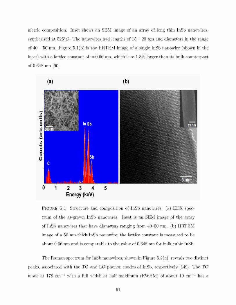
metric composition. Inset shows an SEM image of an array of long thin InSb nanowires,
synthesized at 526oC. The nanowires had lengths of 15 – 20 µm and diameters in the range
of 40 – 50 nm. Figure 5.1(b) is the HRTEM image of a single InSb nanowire (shown in the
inset) with a lattice constant of ≈ 0.66 nm, which is ≈ 1.8% larger than its bulk counterpart
of 0.648 nm [90].
Figure 5.1. Structure and composition of InSb nanowires: (a) EDX spec-
trum of the as-grown InSb nanowires. Inset is an SEM image of the array
of InSb nanowires that have diameters ranging from 40–50 nm. (b) HRTEM
image of a 50 nm thick InSb nanowire; the lattice constant is measured to be
about 0.66 nm and is comparable to the value of 0.648 nm for bulk cubic InSb.
The Raman spectrum for InSb nanowires, shown in Figure 5.2(a), reveals two distinct
peaks, associated with the TO and LO phonon modes of InSb, respectively [149]. The TO
mode at 178 cm−1 with a full width at half maximum (FWHM) of about 10 cm−1 has a
61

very small frequency shift compared to the bulk TO mode [15] at 180 cm−1. Similarly, the
LO mode for the InSb nanowires is at 188 cm−1 with a FWHM of about 6 cm−1, a shift of
about 5 cm−1 compared to the corresponding LO mode [4] in bulk materials at 193 cm−1.
The observation of the two distinct peaks for the TO and LO modes of phonon vibration in
the InSb nanowire sample as well as the fact that the FWHM of the TO and LO lines is ≤
10 cm−1 attests to the high crystalline quality of the InSb nanowires [171].
A small lattice expansion is expected in the InSb nanowire crystal compared to that
of bulk InSb. This is due to the fact that the Bohr radius for InSb is ≈ 60 nm [14] and
the synthesized InSb nanowires had diameters in the range of 40–50 nm. Hence significant
quantum confinement effects are possible, resulting in a minute stress which will result in a
small Raman shift determined by [18]:
(26) ∆ω = −nνωo(a− aoao
)
where n is the dimensionality of the material, ν is the Gruneisen parameter which for InSb
is [106] = 1.3721, and ω0 is the Raman peak position of bulk InSb. Based on equation 26,
the Raman shift caused by stress within the crystal lattice is less than 5 cm−1 for the TO
and LO phonons.
5.5.2. Synthesis of In Nanowires
In nanowires were synthesized using the same experimental set up as that used for
growth of InSb nanowires. However, in this case, the source temperature was raised to 650C,
and the In coated Si substrate was at 600C. After an hour growth, the Si substrate was
found covered with a dense array of nanowires that were over 20 µm long and had diameters
ranging from 40 – 60 nm (shown in inset of Figure 5.3(a)). The EDX spectrum obtained
from these nanowires (Figure 5.3(a)) shows that the process yields metallic In nanowires.
At high temperatures, both the InSb source and the InSb growing crystal loses Sb,
which is driven out of the growth furnace by the carrier gases, resulting in the growth of In
nanowires. The crystal structure of a single 40 nm thick In nanowire was investigated using
62

Figure 5.2. Raman spectrum for InSb, In and Sb nanowires, measured at
room temperature: (a) The deconvoluted Raman spectrum for InSb nanowires
which shows two Raman active modes attributed to TO and LO modes of
phonon vibration in InSb. (b) Raman spectrum for In nanowires which shows
a broad Raman peak at 115 cm−1, attributed to In, while the peak at 521
cm−1 originates from the crystalline Si substrate. (c) Raman spectrum of Sb
nanowires where the characteristic peaks are labeled based on previous studies
on Sb.
HRTEM (Figure 5.3(b)). The inter-planar distance between the lattice fringes is estimated
to be 0.48 nm, comparable to the lattice constant of 0.49 nm for bulk tetragonal In [118].
The Raman spectrum for In nanowires is shown in Figure 5.2(b); the broad Raman peak at
115 cm−1 is most likely attributed to In.
63
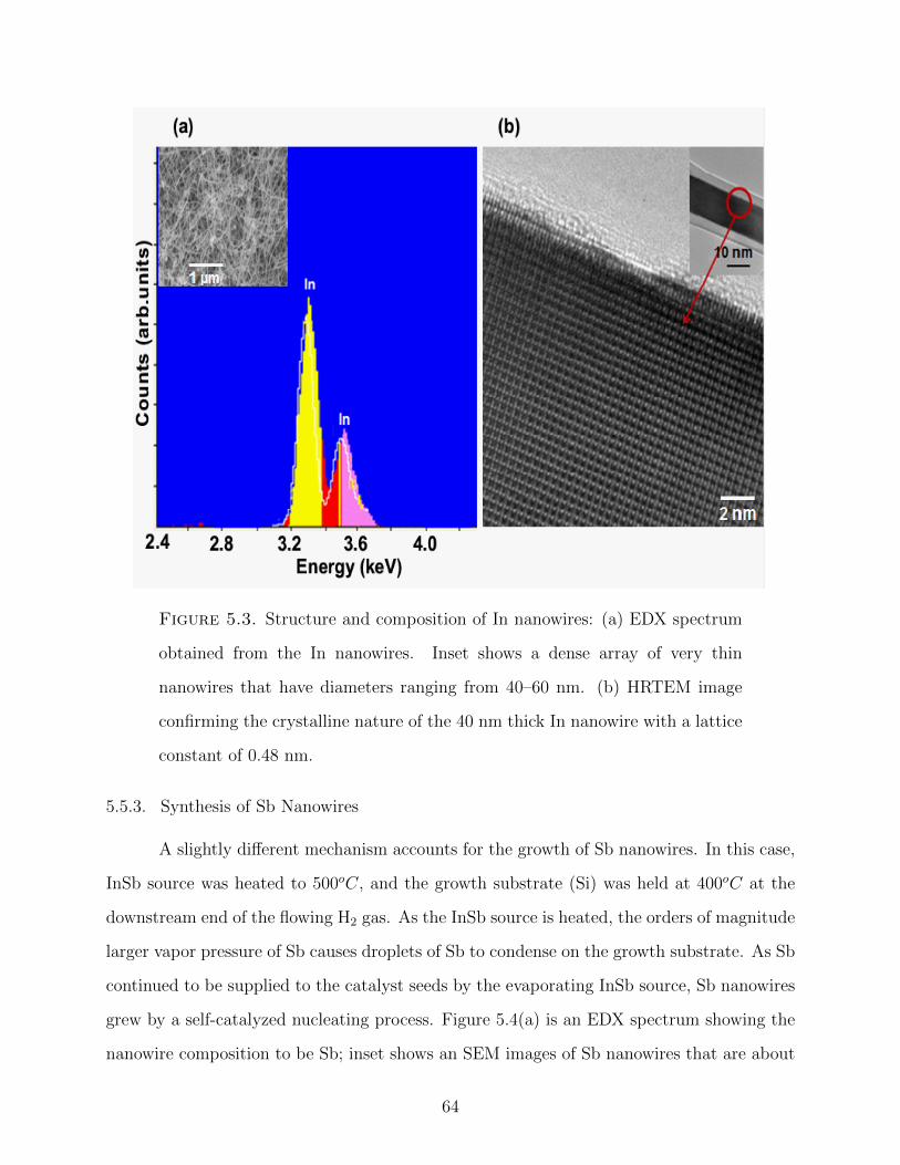
Figure 5.3. Structure and composition of In nanowires: (a) EDX spectrum
obtained from the In nanowires. Inset shows a dense array of very thin
nanowires that have diameters ranging from 40–60 nm. (b) HRTEM image
confirming the crystalline nature of the 40 nm thick In nanowire with a lattice
constant of 0.48 nm.
5.5.3. Synthesis of Sb Nanowires
A slightly different mechanism accounts for the growth of Sb nanowires. In this case,
InSb source was heated to 500oC, and the growth substrate (Si) was held at 400oC at the
downstream end of the flowing H2 gas. As the InSb source is heated, the orders of magnitude
larger vapor pressure of Sb causes droplets of Sb to condense on the growth substrate. As Sb
continued to be supplied to the catalyst seeds by the evaporating InSb source, Sb nanowires
grew by a self-catalyzed nucleating process. Figure 5.4(a) is an EDX spectrum showing the
nanowire composition to be Sb; inset shows an SEM images of Sb nanowires that are about
64

15 µm long and have diameters ranging from 30-50 nm. The corresponding HRTEM image
(Figure 5.4(b)) obtained from a single Sb nanowire shows the lattice fringes corresponding
to crystalline Sb.
Figure 5.4. Structure and composition of Sb nanowires: (a) EDX spectrum
obtained from an array of Sb nanowires; inset shows a dense array of the
as-grown nanowires with diameters ranging from 30–50 nm. (b) Low magnifi-
cation TEM image of a 40 nm thick crystalline Sb nanowire.
The Raman spectrum obtained for Sb nanowires (Figure 5.2(c)) shows characteristic
peaks at 137 and 153 cm−1 and two broad peaks centered at 103 and 271 cm−1. Liu et.
al [109] reported Sb Raman modes at 128 and 158 cm−1, along with a broad weak peak
between 250 and 300 cm−1, attributed to second-order scattering by optical phonon modes.
65

5.6. Electron Transport Measurements
For electrical transport measurements, the nanowires were dispersed on a p+ Si sub-
strate (resistivity of 0.001–0.005 Ωcm) covered with a 200 nm thick SiO2 layer. The location
of the nanowires were identified with respect to pre-patterned markers. Using a patterned
mask two contact pads were established at the nanowire ends, followed by evaporation of
metallic (Au) contacts.
These contacts function as the source and drain electrodes. To facilitate three ter-
minal measurements, the nanowires were used in a field effect transistor type configuration,
with the highly doped p+ Si substrate serving as the back gate. Transport measurements
were performed using a semiconductor parametric analyzer (Agilent Technologies B1500A).
For temperature dependent transport measurements, the samples were placed in a tempera-
ture controlled cryostat (Lakeshore 330), where the temperature was varied from 100 to 450
K.
Current-voltage characteristics of all 3 types of nanowires were obtained by 2-terminal
and 3-terminal measurements. The inset in Figures 5.5 (a) and (b) are SEM image of a single
nanowire contacted by Au electrodes for 2-terminal measurements and a schematic of the de-
vice configuration used for 3-terminal measurements respectively. Temperature dependent 2-
terminal measurements were used to confirm the semiconducting, metallic and semi-metallic
nature of the InSb, In and Sb nanowires. The carrier concentration in these nanowires were
estimated from 3-terminal measurements [145], using the equation: n0=C—VT |/(qπ R2 L);
where the gate capacitance C was estimated from the equation:
(27) C =2πε0εeffL
cosh−1(tox+RR
)εeff ≈ 2.2 is the effective dielectric constant for the SiO2 back-gate dielectric, tox=200 nm
is the dielectric thickness, R is the nanowire radius, and L is the distance between the two
source and drain contacts. Equation 27 describes capacity of a metallic cylinder over a
metallic plane and hence should be adequate if the screening length in the wire rs is much
less than both the wire radius R and the dielectric thickness tox. For metallic In and semi-
66
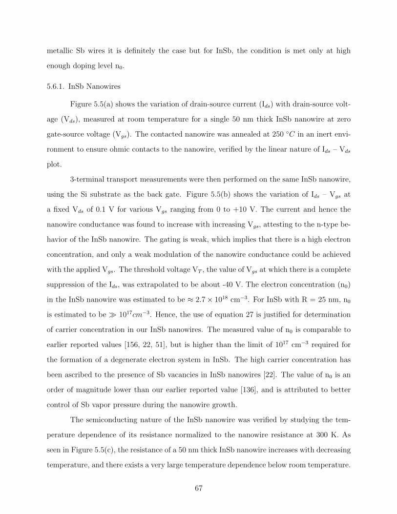
metallic Sb wires it is definitely the case but for InSb, the condition is met only at high
enough doping level n0.
5.6.1. InSb Nanowires
Figure 5.5(a) shows the variation of drain-source current (Ids) with drain-source volt-
age (Vds), measured at room temperature for a single 50 nm thick InSb nanowire at zero
gate-source voltage (Vgs). The contacted nanowire was annealed at 250 C in an inert envi-
ronment to ensure ohmic contacts to the nanowire, verified by the linear nature of Ids – Vds
plot.
3-terminal transport measurements were then performed on the same InSb nanowire,
using the Si substrate as the back gate. Figure 5.5(b) shows the variation of Ids – Vgs at
a fixed Vds of 0.1 V for various Vgs ranging from 0 to +10 V. The current and hence the
nanowire conductance was found to increase with increasing Vgs, attesting to the n-type be-
havior of the InSb nanowire. The gating is weak, which implies that there is a high electron
concentration, and only a weak modulation of the nanowire conductance could be achieved
with the applied Vgs. The threshold voltage VT , the value of Vgs at which there is a complete
suppression of the Ids, was extrapolated to be about -40 V. The electron concentration (n0)
in the InSb nanowire was estimated to be ≈ 2.7× 1018 cm−3. For InSb with R = 25 nm, n0
is estimated to be 1017cm−3. Hence, the use of equation 27 is justified for determination
of carrier concentration in our InSb nanowires. The measured value of n0 is comparable to
earlier reported values [156, 22, 51], but is higher than the limit of 1017 cm−3 required for
the formation of a degenerate electron system in InSb. The high carrier concentration has
been ascribed to the presence of Sb vacancies in InSb nanowires [22]. The value of n0 is an
order of magnitude lower than our earlier reported value [136], and is attributed to better
control of Sb vapor pressure during the nanowire growth.
The semiconducting nature of the InSb nanowire was verified by studying the tem-
perature dependence of its resistance normalized to the nanowire resistance at 300 K. As
seen in Figure 5.5(c), the resistance of a 50 nm thick InSb nanowire increases with decreasing
temperature, and there exists a very large temperature dependence below room temperature.
67

Figure 5.5. Electron transport and temperature dependent resistance mea-
surements on a 50 nm thick InSb nanowire: (a) Variation of drain-source
current (Ids) with drain-source voltage (Vds) at gate bias voltage Vgs = 0 V,
measured after annealing the sample. The linear nature of the Ids–Vds plot
is characteristic of ohmic contacts between the Au electrodes and the InSb
nanowire. Inset shows SEM image of a single nanowire contacted by metal
electrodes. (b) Variation in Ids with positive Vgs, at Vds = 0.1 V. The increase
in Ids with positive Vgs attests to the n-type behavior of the InSb nanowire.
Inset shows a schematic of the 3-terminal device. (c) Temperature dependence
of resistance of InSb nanowires, normalized to nanowire resistance at 300 K.
This dependence is characteristic of semiconductors and is attributed to an
exponential increase in carrier concentration with temperature. (d) Tempera-
ture dependent conductivity measurements (Arrhenius plot) for the extraction
of activation energy from a single InSb nanowire.
68

Such large temperature dependence of resistance has also been observed in InSb thin films [5]
and InSb nanowires [168, 14], and is characteristic of semiconductors where the carrier con-
centration varies exponentially with temperature. An activation energy, characterized by the
linear region in the semi-log plot of conductivity (Figure 5.5(d)), was obtained by fitting the
data to an exponential functional form in the limit of no compensation, using the equation:
(28) σ = σ0exp(−Ea/kBT )
where σ is conductivity of InSb nanowire, σ0 is the pre-exponential factor, kB is the Boltz-
mann’s constant (8.617×10⁻⁵eV K−1) and T is the absolute temperature. From this analysis,
the activation energy Ea is estimated to be 0.11 eV. Due to size quantization, the band gap
of the 50 nm InSb nanowire is estimated to be 0.23 eV. The experimentally determined
Ea matches half the band gap, which is expected for intrinsic charge carriers. For the given
geometry of the nanowire, a resistivity of ≈ 1 Ω.cm was measured; the reason for the high re-
sistivity is most likely due to reduced electron mobility caused by scattering at the nanowire
surface.
5.6.2. In Nanowires
Figure 5.6(a) shows the variation of Ids with Vds at zero Vgs for a single 40 nm diameter
In nanowire contacted by Au electrodes. Compared to the InSb nanowires, the value of Ids
through the In nanowire is several orders of magnitude higher. The linear nature of the Ids–
Vds plot is evidence of ohmic contacts between the In nanowire and the Au electrodes. Using
the p+ Si substrate as a back gate, gate dependent 3-terminal transport measurements were
made on the In nanowire at room temperature. Figure 5.6(b) shows the variation in Ids with
Vgs at fixed Vds = 1.0 V.
As seen in the plot, there is very little dependence of Vgs on Ids. This was tested for
different values of Vds and in all cases, the dependence of Ids on Vgs was very weak. The
slight increase in Ids with positive Vgs attests to the n-type behavior of the In nanowire.
The minimal effect of Vgs on electron transport confirms the presence of a high electron
concentration in the In nanowires, estimated to be ≈ 1.4× 1021 cm−3; which is expected of
69

Figure 5.6. Electron transport and temperature dependence measurements
on a 40 nm thick In nanowire:(a) Variation of drain-source current (Ids) with
drain-source voltage (Vds) at gate bias voltage Vgs = 0 V. The linear nature
of the plot attests to ohmic contacts between the Au electrodes and the In
nanowire. (b) Variation in Ids with Vgs, at Vds = 1.0 V. The weak gating
is due to a high carrier concentration in the In nanowires. (c) Temperature
dependence of resistance of In nanowires, normalized to nanowire resistance
at 300 K. The resistance and hence conductance of the nanowire is almost
independent of temperature below 300 K, but varies significantly at higher
temperature. (d) At the high temperature end, the resistance is found to be
proportional to T3/2 (derived from the slope of ln(R) vs ln(T), which implicates
the involvement of acoustic phonons in electron transport.
70

metallic nanowires.
The normalized temperature dependence of resistance for the In nanowire is shown
in Figure 5.6(c), where the nanowire shows very little change in resistance below 300 K
and a much higher change at higher temperatures. In metals, electron concentration is
temperature-independent and the temperature dependence of resistance is exclusively due
to mobility. At low temperature mobility is determined by impurity and defect scattering and
for metals is temperature-independent. At higher temperatures, phonon scattering becomes
important and mobility drops with temperature due to the increase of the number of phonons,
thus causing an increase in the resistance of the nanowire. The temperature dependence of
resistance for the In nanowire at the high temperature end is plotted in Figure 5.6(d) and
from the straight line fit to this plot, the resistance is found to be proportional to T 3/2, which
confirms that at high temperatures, transport is dominated by acoustic phonon interaction.
5.6.3. Sb Nanowires
2-terminal transport measurements on a single 40 nm diameter Sb nanowire (Fig-
ure 5.7(a)), shows that Ids through the Sb nanowire is an order of magnitude higher than
that through the InSb nanowire, but several orders of magnitude lower than the In nanowire.
Figure 5.7(b) shows the variation in Ids–Vgs at fixed Vds = 0.2 V.
indent The value of current through the Sb nanowire and hence its conductance was found to
decrease with increasing positive Vgs, which implicates the role of holes as majority carriers
in the Sb nanowire. The hole concentration was estimated to be 2.55 × 1019cm−3. Though
semi-metals are characterized by equal concentrations of electrons and holes, even thin films
of Sb show hole-type conductivity, which arises because of the higher mobility of holes com-
pared to that of electrons [100, 71]. The hole dominated conductivity can also be explained
in terms of surface states, which can be either donor or acceptor type, which in the case of
the 40 nm Sb nanowire will noticeably change the free carriers and result in violation of the
n = p rule for semi-metals.
Temperature dependence of resistance for the 40 nm thick Sb nanowire shows an
increase in nanowire resistance with temperature (Figure 5.7(c)). Based on transport mea-
71

Figure 5.7. Electron transport and temperature dependence measurements
on a 40 nm thick Sb nanowire(a) Variation of drain-source current (Ids) with
drain-source voltage (Vds) at gate bias voltage Vgs = 0 V. The magnitude of
Ids is higher than that obtained for InSb nanowires, but much lower than that
for In nanowires. (b) Variation in Ids with positive Vgs, measured at Vds = 0.2
V. The decrease in Ids with incease in Vgs attests to a p-type behavior for the
Sb nanowires. (c) Temperature dependence of resistance of Sb nanowires, nor-
malized to nanowire resistance at 300 K. The dependence is relatively weak at
temperatures below 200 K due to reduced contribution from phonon scattering
at low temperatures.
surements, the Sb nanowires are almost metallic. Due to the overlap between the conduction
and valence bands in Sb, the carrier density is a weak function of temperature and the effect
of temperature on resistance is mainly determined by the temperature dependence of various
72

scattering mechanisms: (i) the hole-phonon scattering which increases with temperature and
(ii) hole-boundary scattering which is not significantly affected by temperature. At temper-
atures above 200 K, phonon scattering dominates and as shown in Figure 5.7(c), there is a
significant increase in resistance with temperature. However, as the temperature is reduced,
the contribution from phonon scattering is not significant and boundary scattering becomes
dominant. This accounts for the relatively low dependence of resistance on temperatures
below 200 K.
5.7. Conclusion
Semiconducting InSb, metallic In and semi-metallic Sb nanowires were synthesized by
chemical vapor deposition. The unique properties of the as-grown crystalline nanowires were
determined through electron transport measurements and temperature dependent resistance
measurements. The estimated electron concentration in semiconducting InSb nanowires
(1018 cm−3) was found to be orders of magnitude lower than that in metallic In nanowires,
which had an electron concentration of the order of 1021 cm−3.
Temperature dependent resistance measurements on InSb nanowires showed typical
semiconducting behavior with a negative temperature coefficient of resistance below room
temperature, attributed to the exponential increase in carrier concentration with tempera-
ture. In contrast, the resistance of metallic In nanowires showed very little change below
room temperature and a strong increase at higher temperatures. This phenomena is ex-
plained on the basis of carrier mobility affecting the temperature dependence of resistance in
metals. Below room temperature mobility is determined by impurity and defect scattering,
which is temperature-independent. However, at higher temperatures mobility decreases due
to electron-phonon scattering, thus causing an increase in the resistance of the nanowire. At
the high temperature end, the resistance of In nanowires were found to be proportional to
T3/2, confirming the role of acoustic phonons in electron transport. The Sb nanowires showed
hole dominated conductivity which could be due to higher mobility of holes compared to
that of electrons or due to the presence of surface states. Further experiments are required
to investigate the nature and role of surface states in Sb nanowires. Temperature dependent
73

resistance measurements showed hole-phonon scattering dominating at higher temperatures,
following a trend similar to that observed in metallic In nanowires.
74
CHAPTER 6
INDIUM OXIDE NANOWIRES FOR GAS SENSING APPLICATION1
6.1. Introduction
A gas sensor is a device that can be used to detect various gases such as CO2, CO,
O2, and NH3. In the past decade, gas sensors based on various metal oxide semiconductors
(MOS) have been extensively studied for wide application such as environmental monitoring,
indoor air quality, workplace health and safety and homeland security. Various attempts
have been made to develop sensing devices with high sensitivity, stability, and rapid re-
sponse [77, 141, 99].
The first generation of MOS gas sensors was reported by Taguchi [35]. They were
based on thick SnO2 film and have various advantages such as small size, low-power-consumption [35],
simple construction, good sensing properties [12], and high compatibility with microelec-
tronic processing [34].
The sensitivity of the sensors strongly depend on the morphology of MOS in spite of
the same basic gas sensing mechanism (adsorption and desorption of gas molecules). Com-
pared to the sensors based on thin films, the nanowire gas sensors exhibit many interesting
characteristics such as ultra-sensitivity and fast response time. Due to their high surface-
to-volume ratio of the nanowire sensors, a few gas molecules are sufficient to change the
electrical properties of the sensing elements. Thus it is possible to detect very low concen-
tration of gas within several seconds. Very small amounts of gas can change the electrical
characteristics of nanowires which enable nanowire sensors to respond at lower-operating
temperature.
6.2. Experimental Details
In2O3 nanowires were synthesized using using CVD method shown in Figure 1.3
(Chaper1).Pure InSb powder (Alpha Aesar, 99.99 % purity) was used as the source material
1Parts of this capter are reproduced from Pradeep Gali, Gopal Sapkota, A.J. Syllaios, Chris littler,and U. Philipose, ”Stoichiometry dependent electron transpor and gas sensing properties of indium oxidenanowires,” Nanotechnology,, 24, 225704, 2013 with permission from IOP.
75

and placed in an alumina boat at the center of the quartz tube. Si substrates were cleaned
by sonicating first with acetone and then with alcohol for about 10 minutes, followed by
deionised water rinse before thermal evaporation of catalyst seed layer. Then, Si substrate
coated with 300 nm thick In film was placed ‘face down’ right above the source. The source
and substrate temperature were maintained at ≈ 625C. Under the constant flow of 50 sccm
of oxygen, In2O3 nanowires were grown for 1-2 hours.
6.3. Structural Characterization
In order to obtain morphological information, the nanowires grown under different
growth conditions were investigated using a scanning electron microscope (SEM: Hitachi
SU1510), equipped with energy dispersive X-ray (EDX) spectrometer. The nanowires were
found to be several microns long and had diameters in the range of 40–80 nm as shown in
Figure 6.1 (a). The EDX spectrum obtained from these nanowires (Figure 6.1(b)) confirmed
that grown nanowires were In2O3 nanowires.
6.4. Results and Discussion
A single In2O3 nanowire was contacted by two Au electrodes after dispersed on a
p+ Si substrate covered with a 200 nm thick SiO2. For study of its gas sensing properties,
that device was kept in a sealed enclosure provided with electrical feed-throughs. Gas sens-
ing properties of the device were studied by measuring the change in conductivity of the
nanowire as a result of gas adsorption at zero gate bias using Agilent Technologies B1500A
semiconductor device analyzer.Transport measurements were also made on In2O3 nanowires
that were annealed at 600C in wet oxygen ambient, post-growth, to confirm that oxygen
vacancies are responsible for the relatively high electron carrier concentration in the as-grown
In2O3 nanowires.
The gas sensing properties of two separate devices were studied. Device A is com-
prised of an as-grown single In2O3 nanowire, contacted by annealed Au electrodes; while
device B was an In2O3 nanowire that was annealed in O2 post-growth to reduce the num-
ber of oxygen vacancies in the crystal lattice. The performance of any nanowire-based gas
76
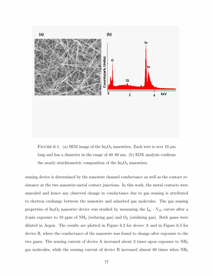
( a ) ( b )
Figure 6.1. (a) SEM image of the In2O3 nanowires. Each wire is over 10 µm
long and has a diameter in the range of 40–80 nm. (b) EDX analysis confirms
the nearly stoichiometric composition of the In2O3 nanowires.
sensing device is determined by the nanowire channel conductance as well as the contact re-
sistance at the two nanowire-metal contact junctions. In this work, the metal contacts were
annealed and hence any observed change in conductance due to gas sensing is attributed
to electron exchange between the nanowire and adsorbed gas molecules. The gas sensing
properties of In2O3 nanowire device was studied by measuring the Ids - Vds curves after a
2-min exposure to 10 ppm of NH3 (reducing gas) and O2 (oxidizing gas). Both gases were
diluted in Argon. The results are plotted in Figure 6.2 for device A and in Figure 6.3 for
device B, where the conductance of the nanowire was found to change after exposure to the
two gases. The sensing current of device A increased about 3 times upon exposure to NH3
gas molecules, while the sensing current of device B increased almost 60 times when NH3
77
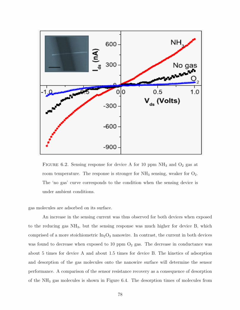
Figure 6.2. Sensing response for device A for 10 ppm NH3 and O2 gas at
room temperature. The response is stronger for NH3 sensing, weaker for O2.
The ‘no gas’ curve corresponds to the condition when the sensing device is
under ambient conditions.
gas molecules are adsorbed on its surface.
An increase in the sensing current was thus observed for both devices when exposed
to the reducing gas NH3, but the sensing response was much higher for device B, which
comprised of a more stoichiometric In2O3 nanowire. In contrast, the current in both devices
was found to decrease when exposed to 10 ppm O2 gas. The decrease in conductance was
about 5 times for device A and about 1.5 times for device B. The kinetics of adsorption
and desorption of the gas molecules onto the nanowire surface will determine the sensor
performance. A comparison of the sensor resistance recovery as a consequence of desorption
of the NH3 gas molecules is shown in Figure 6.4. The desorption times of molecules from
78

Figure 6.3. (a) Sensing response for device B for 10 ppm NH3 gas at room
temperature. The sensing current increased about 60 times when NH3 gas
molecules are adsorbed on the nanowire surface. The sensing current under
‘no gas’ condition (nanowire is under ambient conditions) is shown enhanced
10 times for comparison. (b) Sensing response for device B for 10 ppm O2 gas
at room temperature. There is a weak response (decrease) in sensing current.
device B is shorter than that for device A; thus confirming that the stoichiometry of In2O3
nanowires plays a significant role in its gas sensing properties.
The enhanced gas sensing performance of mechanism of device B in comparison to
device A, for the reducing gases can be explained on the basis of an energy band diagram,
in terms of the chemisorption of gas molecules on the nanowire surface [104] and the corre-
sponding effect on electron transport. Since the In2O3 nanowire is determined to be n-type,
EF is shifted closer to Ec, compared to its intrinsic position in the band gap, but it is still
79

Figure 6.4. In2O3 nanowire gas sensor response as NH3 molecules are des-
orbed from the nanowire surface.
several kT away from the conduction band edge. Despite the ohmic nature of the contacts, a
short barrier φMS exists at the Au- In2O3 interface, as shown in the schematic band diagram
of Figure 6.5. The height of this barrier is dependent on the stoichiometry of the nanowire
and is determined by the Debye length LD (where LD ∝ 1√n
where n is the charge carrier
density [46, 93]). Device A (LD ≈ 3 nm) has a lower φMS, when compared to device B (LD
is about 10 times higher) which has a larger φMS. When molecules of reducing gases like
NH3 are adsorbed on the nanowire surface, its electron donating nature and the difference
in chemical potentials of In2O3 and NH3 [30] causes electrons to transfer into the nanowire,
thus increasing the conductivity of the n-type semiconductor channel device. This effect is
significantly enhanced in device B as compared to device A. This is because φMS is much
larger in device B and there is a significant lowering of barrier height when NH3 molecules
80

adsorb on the nanowire surface. The enhanced sensor response is attributed to a change in
the nanowire channel conductance as a consequence of a large decrease in φMS during the
sensing of NH3 gas.
Figure 6.5. Schematic of gas sensing mechanism explained in terms of en-
ergy band diagram for: (a) Device A comprising of a single as-grown In2O3
nanowire, with poor stoichiometry; (b) Device B comprising of a single In2O3
nanowire, that was annealed in O2 leading to improved stoichiometry.
On the other hand, when O2, which is an oxidizing gas is adsorbed on the nanowire
surface, its electron withdrawing nature reduces the nanowire channel conductivity for both
devices. The adsorbed oxygen on the nanowire surface further depletes its conduction chan-
nel, thus resulting in an increase in φMS and a decrease in conductance. The decrease in
channel conductance for the oxidizing gases is more significant in device A than in device B.
The improved sensor performance of device A is again attributed to an increase in φMS when
81

O2 gas molecules are adsorbed on the nanowire surface. This effect is not as pronounced in
device B which had a significantly higher initial φMS.
Device A, comprising of a single In2O3 nanowire with poor stoichiometry and high
carrier concentration was found to be about 3 times more efficient at sensing oxidizing gases
than device B, which comprised of a single In2O3 nanowire with good stoichiometry and
lower carrier concentration. On the other hand device B was found to be about 20 times
more efficient than device A at sensing reducing gases. These results are promising because
it shows that nanowire stoichiometry and the type of gas molecules can be used for gating
effects to modulate the nanowire conductance.
6.5. Conclusions
In2O3 nanowires were successively synthesized using CVD system.Gas sensing prop-
erties of the device were studied by measuring the change in conductivity of the nanowire
as a result of gas adsorption at zero gate bias. An increase in conductance was observed
when reducing gas molecules of NH3 are adsorbed on the nanowire surface, while a decrease
in conductance was observed for the oxidizing molecules of O2. The stoichiometric In2O3
nanowires was a more efficient gas sensor of reducing gases, while the non-stoichiometric
nanowires were more efficient for the oxidizing gases.
82

CHAPTER 7
LOW TEMPERATURE SYNTHESIS OF IRON DOPED ZINC OXIDE NANOWIRES
AND NANOTUBES1
7.1. Introduction
Zinc oxide (ZnO), a direct wide band gap semiconductor, has been studied extensively
since the 1930s [19]. ZnO has been shown to produce a rich family of different nanostructures
with wurtzite structure with total of 13 different facet growth directions [96, 142]. Due to
the ionic character of the polar surfaces, ZnO can be synthesized in a variety of morpho-
logically different nanostructures such as: nanorods, nanobelts, nanocombs, nanosprings,
nanorings, nanobows, nanojunction arrays, and nano-propeller arrays [40]. Currently ZnO
nanostructures attract intense global interest due to the possibility of making low energy
and environmentally friendly light emitting devices and laser diodes operating above room
temperature. Of the different morphologies of nanostructures, nanotubes are considered
promising for applications such as in dye-sensitized solar cells and sensors with improved
performance and higher sensitivity. This is because, in contrast to nanowires and nanorods,
the pores in nanotubes can be filled with nanoparticles or dyes, enabling tuning of the spec-
tral response. These properties make ZnO nanotube arrays suitable for diverse application
such as in measurements of intracellular biochemical species within single living cells, in
photocatalysis, solar cells, chemical sensors, and optoelectronics. The possibility of synthe-
sizing ferromagnetic ZnO nanotubes is particularly promising since this will allow for several
promising applications in the field of spintronic and opto-electronics [36, 59, 152, 131]. To
this end, the focus of this work was directed towards developing a simple synthesis route
for the development of a dilute magnetic semiconductor, using a time efficient process, in a
morphology that would enable tuning of band gap and hence spectral response.
The Fe-doped ZnO nanotubes were synthesized by simple electrochemical process
1This entire capter is reproduced from Gopal Sapkota, Karol Gryczynsky, Roy Mcdougald, Arup Neogi,and U. Philipose, ’Low-temperature synthesis of Fe-doped ZnO nanotubes,” J. Electronic Materials, 41, 8,2012 with permission from Springer.
83

at 75C using ZnCl2 and KCl mixed with Fe as an electrolyte. The growth process was
optimized for obtaining high quality ZnO nanotubes through critical control of the growth
parameters, such as the electrolyte concentration and the growth time. Our growth technique
is a single step process in which metastable polar plane (0001) of ZnO is exploited for the
formation of nanotubes. We observed that Fe contained in the solution accelerates the etching
process, thus effectively reducing the growth time, in comparison with earlier reported works
on undoped ZnO nanotubes [2, 78, 162, 73, 101, 119, 151, 27, 68, 150, 86, 52, 147, 113, 161,
85, 7].
7.2. Experimental Details
Synthesis of ZnO nanotubes was done in a three electrode standard electrochemical
cell with a Si (111) substrate coated with 300 nm Au film as the cathode and the working
electrode. The counter electrode was made of Pt. All the reagents (Alfa Aesar) used were
analytical grade and used without further purification. Prior to Au evaporation, the sub-
strates were cleaned by sonicating them first in acetone and then in alcohol for about 10
minutes, followed by a deionized water rinse. Two concentrations of electrolytes were used in
this experiment: electrolyte A, comprising of a mixture of [FeCl3 (0.1 mM) + ZnCl2 (6 mM)
+ KCl (0.2 M)]; and electrolyte B, comprising of a mixture of [ FeCl3 (0.1 mM) + ZnCl2 (5
mM) + KCl (0.1 M)]. Homogeneous electrolyte solutions were prepared by sonicating the
mixture in a warmed ultrasonic bath. Synthesis was carried out in a temperature controlled
water bath maintained at 75C. Oxygen (20 sccm) was continuously bubbled through the
electrolyte during the growth process. A constant bias of -1 V was maintained between the
working and reference electrodes during the growth process.
Post-growth, the nanostructures were characterized by scanning electron microscope
(SEM) (NOVA dual beam SEM/FIB, FEI Nova 200 Nano-Lab), a high resolution trans-
mission electron microscope (HRTEM) (FEI Tecnai G2 F20 S-Twin 200 keV) and selected
area electron microscopy (SAED) pattern analysis. Composition and structural analysis
were further done by energy-dispersive X-ray spectroscopy (EDX) and an X-ray diffraction
(XRD) (Rigaku Ultima III). Following structural characterization, the nanostructures were
84
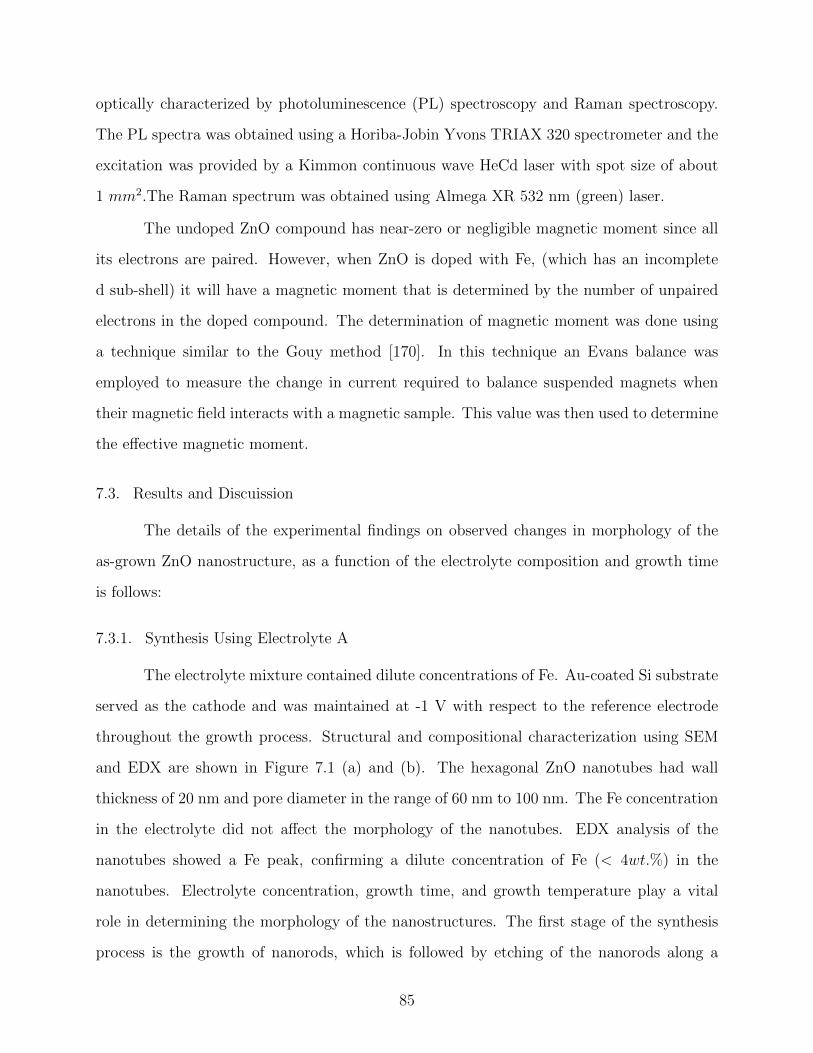
optically characterized by photoluminescence (PL) spectroscopy and Raman spectroscopy.
The PL spectra was obtained using a Horiba-Jobin Yvons TRIAX 320 spectrometer and the
excitation was provided by a Kimmon continuous wave HeCd laser with spot size of about
1 mm2.The Raman spectrum was obtained using Almega XR 532 nm (green) laser.
The undoped ZnO compound has near-zero or negligible magnetic moment since all
its electrons are paired. However, when ZnO is doped with Fe, (which has an incomplete
d sub-shell) it will have a magnetic moment that is determined by the number of unpaired
electrons in the doped compound. The determination of magnetic moment was done using
a technique similar to the Gouy method [170]. In this technique an Evans balance was
employed to measure the change in current required to balance suspended magnets when
their magnetic field interacts with a magnetic sample. This value was then used to determine
the effective magnetic moment.
7.3. Results and Discuission
The details of the experimental findings on observed changes in morphology of the
as-grown ZnO nanostructure, as a function of the electrolyte composition and growth time
is follows:
7.3.1. Synthesis Using Electrolyte A
The electrolyte mixture contained dilute concentrations of Fe. Au-coated Si substrate
served as the cathode and was maintained at -1 V with respect to the reference electrode
throughout the growth process. Structural and compositional characterization using SEM
and EDX are shown in Figure 7.1 (a) and (b). The hexagonal ZnO nanotubes had wall
thickness of 20 nm and pore diameter in the range of 60 nm to 100 nm. The Fe concentration
in the electrolyte did not affect the morphology of the nanotubes. EDX analysis of the
nanotubes showed a Fe peak, confirming a dilute concentration of Fe (< 4wt.%) in the
nanotubes. Electrolyte concentration, growth time, and growth temperature play a vital
role in determining the morphology of the nanostructures. The first stage of the synthesis
process is the growth of nanorods, which is followed by etching of the nanorods along a
85

Figure 7.1. SEM image of nanotubes grown using electrolyte A for 90 min-
utes: (a) Fe doped ZnO nanotubes with wall thickness of about 20 nm and
pore diameter of about 60-100 nm. Inset shows a magnified SEM image of a
single Fe-doped ZnO nanotube. (b) EDX spectrum confirming the presence of
Fe, Zn and O. The Fe concentration is estimated to be about 3-4 wt%.
specific plane. The etching process is facilitated by the high concentration of KCl in the
electrolyte. Study of the nanotube formation process showed that, during the first period of
45 min, ZnO nanorods were formed, as shown in the SEM image of Figure 7.2. However, after
1 h, the nanowire growth process was terminated due to reduced concentration of Zn 2+ ions
in the electrolyte. Subsequently, KCl etches through the nanowires to form nanotubes. This
is evident in the structure of the nanotubes formed after 90 min of growth time (Figure 7.1
(a)).
86
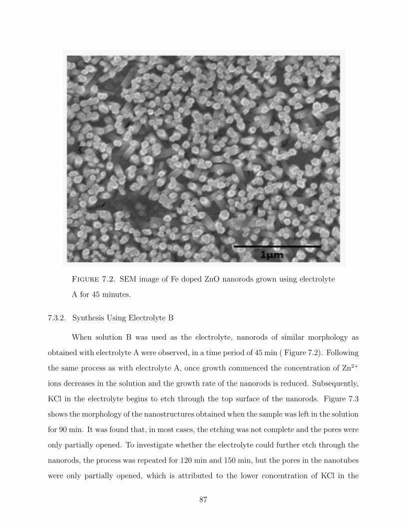
Figure 7.2. SEM image of Fe doped ZnO nanorods grown using electrolyte
A for 45 minutes.
7.3.2. Synthesis Using Electrolyte B
When solution B was used as the electrolyte, nanorods of similar morphology as
obtained with electrolyte A were observed, in a time period of 45 min ( Figure 7.2). Following
the same process as with electrolyte A, once growth commenced the concentration of Zn2+
ions decreases in the solution and the growth rate of the nanorods is reduced. Subsequently,
KCl in the electrolyte begins to etch through the top surface of the nanorods. Figure 7.3
shows the morphology of the nanostructures obtained when the sample was left in the solution
for 90 min. It was found that, in most cases, the etching was not complete and the pores were
only partially opened. To investigate whether the electrolyte could further etch through the
nanorods, the process was repeated for 120 min and 150 min, but the pores in the nanotubes
were only partially opened, which is attributed to the lower concentration of KCl in the
87

electrolyte.
Figure 7.3. SEM image of Fe doped ZnO nanorods grown using electrolyte
B for 90 minutes. Inset shows a single nanotube with partially etched pore.
7.3.3. Growth Mechanism of Nanotubes
Electrochemical growth of ZnO nanorods occurs by O2 reduction in a solution of
ZnCl2 as zinc precursor and KCl as electrolyte according to the reaction (1) and (2) as
follows:
(29) O2 + 2H2O + 4e− → 4OH−
and
(30) Zn2+ + 2OH− → ZnO +H2O
88

The mechanism of formation of the nanotubes following the growth of the nanorods is ex-
plained as; during the growth process, the concentration of Zn2+ in the electrolyte continu-
ously decreases; then, after a critical time period that is dependent on the concentration of
the electrolyte, no further growth is possible. The next step in the electrochemical process
is the role played by the supporting electrolyte KCl. The Cl− ions in KCl are responsible for
the dissolution of the core of the ZnO nanorods. A dependence of the nanotubes pore depth
on the concentration of KCl was observed. With electrolyte A, where the KCl concentration
is 0.2 M, it was possible to obtain nanotubes with fully opened pores. This was not possible
with electrolyte B, where the KCl concentration is lower (0.1 M). The effect of a higher Cl−
ion concentration in electrolyte A, on the etching process can be explained on the basis of
the ZnO crystal structure. ZnO crystal has two polar surfaces perpendicular to the [0001]
growth direction. These surfaces which are either Zn2+ (or Fe2+) or O2− terminated on the
(0001) and (0001) surface respectively, induce a net electrostatic dipole moment parallel to
the c-axis [60]. In addition to the two polar basal planes (0001)/ (0001), ZnO also has six
non-polar planes, (1010), parallel to the c-axis [101]. The non-polar planes have lower surface
energy compared to polar planes so that these planes are more stable than the polar planes
which are metastable [36]. Thus the etching rate is different in polar and non-polar planes
which accounts for the formation of nanotubes. The Cl− ions are preferentially adsorbed
onto the (0001) polar surface and in the Zn2+ or Fe2+ terminated surface; this will lead to
the formation of water soluble chlorides like ZnCl2 or FeCl3. A higher concentration of Cl−
in the electrolyte will ensure that the core of the nanowire is completely etched to form the
nanotubes (Figure 7.1 (a)). Our results show that with electrolyte B, the concentration of
Cl− ions is not sufficient to cause complete dissolution of the nanorods core (Figure 7.3).
The above described mechanism for the formation of nanotubes is very similar to earlier
reported works [2, 78, 162, 73, 101, 119, 151, 27, 68, 150, 86, 52, 147, 113, 161, 85, 7]; the
difference being that contrary to a two-step process involving growth and etching, the pro-
cess we report on is a one step process that is performed in the presence of Fe ions in the
electrolyte. Research is underway to determine whether Fe concentration in the electrolyte
89
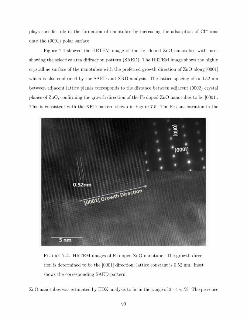
plays specific role in the formation of nanotubes by increasing the adsorption of Cl− ions
onto the (0001) polar surface.
Figure 7.4 showed the HRTEM image of the Fe- doped ZnO nanotubes with inset
showing the selective area diffraction pattern (SAED). The HRTEM image shows the highly
crystalline surface of the nanotubes with the preferred growth direction of ZnO along [0001]
which is also confirmed by the SAED and XRD analysis. The lattice spacing of ≈ 0.52 nm
between adjacent lattice planes corresponds to the distance between adjacent (0002) crystal
planes of ZnO, confirming the growth direction of the Fe doped ZnO nanotubes to be [0001].
This is consistent with the XRD pattern shown in Figure 7.5. The Fe concentration in the
Figure 7.4. HRTEM images of Fe doped ZnO nanotube. The growth direc-
tion is determined to be the [0001] direction; lattice constant is 0.52 nm. Inset
shows the corresponding SAED pattern.
ZnO nanotubes was estimated by EDX analysis to be in the range of 3 - 4 wt%. The presence
90

of Fe was also detected in single nanotubes; where Fe most likely replaces Zn in the ZnO
lattice. HRTEM analysis was done on several Fe doped nanotubes and no trace of secondary
phases or precipitates was observed on the nanotubes. Evidence of the incorporation of Fe
as a substitutional dopant in the ZnO lattice was obtained through XRD measurement and
PL as well as Raman spectroscopy.
Figure 7.5 showed results of an XRD measurement on undoped and doped nanotubes.
The diffraction peaks have been indexed to the hexagonal ZnO wurtzite structure. The
strong peak at 2 = 34.340 corresponds to the (0002) c-axis of ZnO which indicates that the
nanotubes preferentially grow along (0001) direction. No additional peak attributed to Fe
or its oxide could be detected in the XRD spectrum of Fe doped ZnO nanotubes, though
a small shift of the (0002) peak was observed. This shift of the (0002) peak position for
the Fe doped ZnO indicates that there is an increase in the c-axis lattice parameter for the
Fe doped sample, indicative of the fact that Fe ions substitute for Zn as 2+ ions in the
ZnO lattice, without changing its wurtzite crystal structure. Similar results were observed
in Co doped, V doped and Fe doped ZnO thin films [76, 65, 66]. Dependence of the c-axis
lattice constant on Fe content in ZnO has been studied by Fenga et al. [114]. The ionic
radius of Fe2+ is larger than that of Zn2+ by about 5 % [172] and hence if Fe2+ ions occupy
the Zn2+ sites of ZnO, the in-plane atomic arrangement with closed atomic packing will be
strained due to the substitution of Zn with a larger Fe atom. This cause an increase in the
c-lattice constant and a shift of the (0002) peak to a smaller angle in the XRD pattern of the
Fe doped ZnO nanotubes. It is also possible that Fe2+ and Fe3+ ions are both present and
occur as substitutional as well as interstitial dopants. In this case, the atomic arrangement is
disturbed and the number of interstitials will increase, which will result in lattice disorder and
strain. A comparison of the XRD spectrum of the undoped and doped nanotubes (inset of
Figure 7.5) shows that the full-width at half maximum (FWHM) of the (002) diffraction peak
is broadened (about 3% to 4%) and its intensity decreased in the Fe-doped ZnO nanotubes.
This indicates that the dilute (< 4wt.%) Fe doping influences the crystalline quality of the
nanotubes by causing lattice defects. This result was further validated by comparison of the
91
PL spectra before and after doping.
Figure 7.5. XRD spectrum of undoped (solid line) and Fe doped (dotted
line) ZnO nanotubes. Inset shows the broadening of (0002) peak for Fe doped
nanotubes.
Figure 7.6 showed the room temperature PL spectra for the undoped Fe doped ZnO
nanotubes. The curves with solid lines and symbols represent the experimentally obtained
curves for the undoped and Fe doped ZnO nanotubes. The broad defect peak in the Fe doped
sample was de-convoluted using a Gaussian distribution (shown by dashed curves). The PL
spectra for undoped ZnO tubes showed strong band edge emission at 370.5 nm (3.35eV)
and no other peaks, attesting to the high crystalline quality of the undoped nanotubes.
However, when doped with Fe, the PL spectrum showed a UV emission peak at ≈ 381 nm
(red shifted) and a broad emission peak in the visible region. The red-shift of the band edge in
transition-metal- doped II-VI semiconductors has been attributed to the sp-d spin-exchange
92

interactions between the band electrons and localized d electrons of the Fe ion substituting
the group II ion. A Fe2+ cation is in 3d6 configuration. The s-p and p-d exchange interactions
between ZnO as host and Fe as dopant gives rise to a negative and positive correction to
conduction and valence bad edge, leading to narrowing of the band gap [38]. Thus, the red
shift and quenching of the UV emission peak in the doped sample is further evidence of the
fact that Fe substitutes for Zn in the ZnO crystal [8]. The broad defect-related emission
peak is de-convoluted into Gaussian peaks at 474 nm, 489 nm, 499 nm, 551 nm and 563 nm.
The peak observed at 474 nm is attributed to interstitials of Zn and oxygen [9]. The peaks
at 489 nm and 499 nm are attributed to singly ionized oxygen vacancies [157] whereas peaks
at 551 nm and 563 nm are attributed to oxygen interstitial [31].
Figure 7.7 a and b compare the Raman spectrum for the undoped and Fe-doped ZnO
nanotubes. Both samples showed a Raman shift at 521 cm−1 corresponding to the Si sub-
strate used for the growth of ZnO nanotubes. The undoped sample showed a characteristic
Raman peak at 438 cm−1, related to the hexagonal wurtzite phase of ZnO. The Fe-doped
sample shows additional peaks at 336 cm−1, 384 cm−1, and 644 cm−1. The peaks at 336
cm−1 and 384 cm−1 are attributed to intrinsic defects in ZnO such as oxygen vacancies and
zinc interstitials [16]. The additional vibrational mode at 644 cm−1 in the Fe-doped ZnO
nanotubes is also related to intrinsic ZnO lattice defects, which either become activated as
vibrating complexes upon addition of Fe, or their concentration increases upon Fe incorpora-
tion into the ZnO lattice. Such additional modes have been observed in Fe-doped ZnO thin
films and nanostructures [16, 20]. Further evidence of the successful incorporation of Fe into
ZnO was obtained through determination of effective magnetic moment (µeff ) for undoped
and Fe doped ZnO nanotubes. This was done using a magnetic susceptibility balance (Evans
balance), which measures the force experienced by a substance when it is placed in a mag-
netic field. The nanotubes were placed in a cylindrical tube, which was placed in a uniform
magnetic field. The effective magnetic moment was measured in units of Bohr magnetron
(µB) using the expression:
(31) µeff = 2.828(χAT )1/2
93
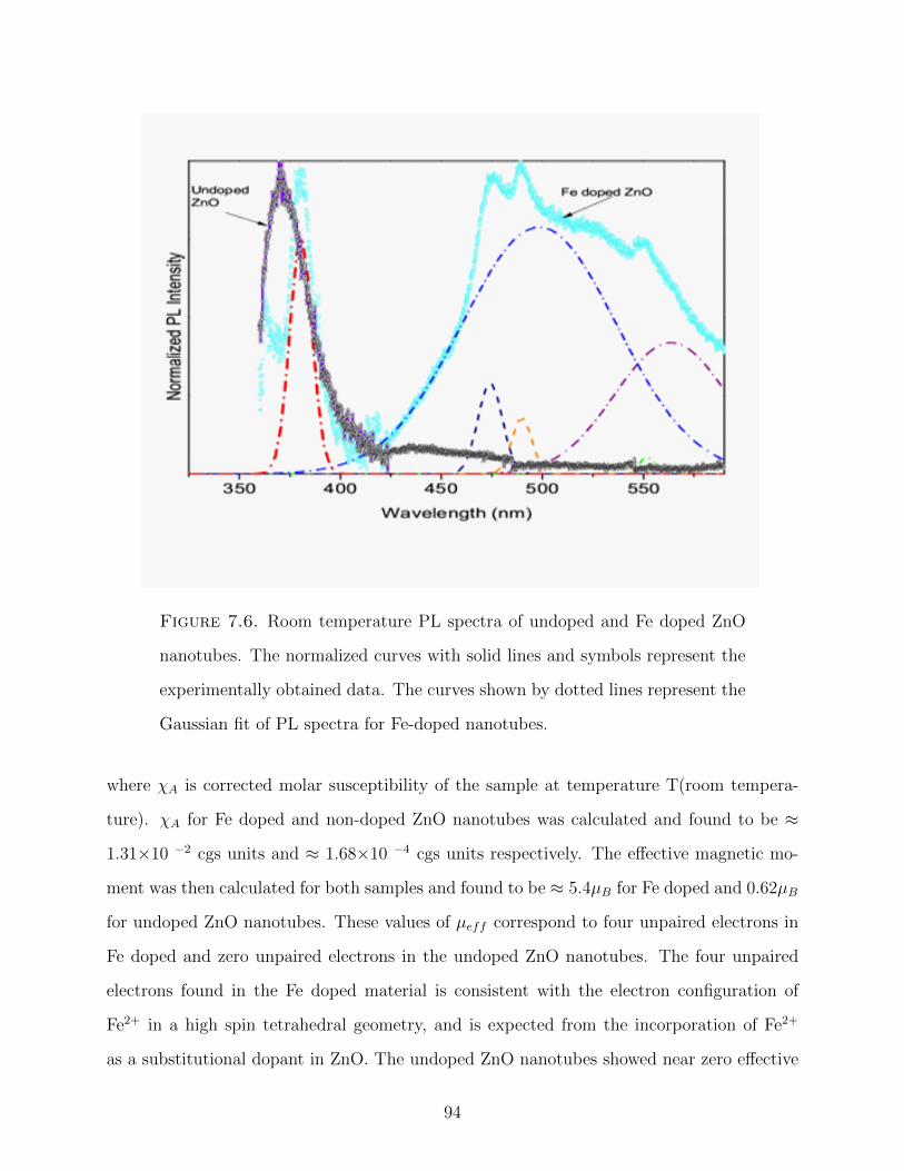
Figure 7.6. Room temperature PL spectra of undoped and Fe doped ZnO
nanotubes. The normalized curves with solid lines and symbols represent the
experimentally obtained data. The curves shown by dotted lines represent the
Gaussian fit of PL spectra for Fe-doped nanotubes.
where χA is corrected molar susceptibility of the sample at temperature T(room tempera-
ture). χA for Fe doped and non-doped ZnO nanotubes was calculated and found to be ≈
1.31×10 −2 cgs units and ≈ 1.68×10 −4 cgs units respectively. The effective magnetic mo-
ment was then calculated for both samples and found to be ≈ 5.4µB for Fe doped and 0.62µB
for undoped ZnO nanotubes. These values of µeff correspond to four unpaired electrons in
Fe doped and zero unpaired electrons in the undoped ZnO nanotubes. The four unpaired
electrons found in the Fe doped material is consistent with the electron configuration of
Fe2+ in a high spin tetrahedral geometry, and is expected from the incorporation of Fe2+
as a substitutional dopant in ZnO. The undoped ZnO nanotubes showed near zero effective
94
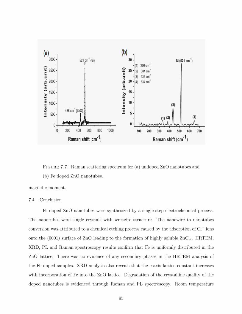
Figure 7.7. Raman scattering spectrum for (a) undoped ZnO nanotubes and
(b) Fe doped ZnO nanotubes.
magnetic moment.
7.4. Conclusion
Fe doped ZnO nanotubes were synthesized by a single step electrochemical process.
The nanotubes were single crystals with wurtzite structure. The nanowire to nanotubes
conversion was attributed to a chemical etching process caused by the adsorption of Cl− ions
onto the (0001) surface of ZnO leading to the formation of highly soluble ZnCl2. HRTEM,
XRD, PL and Raman spectroscopy results confirm that Fe is uniformly distributed in the
ZnO lattice. There was no evidence of any secondary phases in the HRTEM analysis of
the Fe doped samples. XRD analysis also reveals that the c-axis lattice constant increases
with incorporation of Fe into the ZnO lattice. Degradation of the crystalline quality of the
doped nanotubes is evidenced through Raman and PL spectroscopy. Room temperature
95

PL spectra show strong UV emission for undoped ZnO nanotubes. This emission is red
shifted for Fe doped ZnO nanotubes and is attributed to spd spin- exchange interactions
between the band electrons and the localized d electrons of Fe2+ substituting for Zn2+ in the
ZnO lattice. Determination of the effective magnetic moment using a magnetic susceptibility
balance shows the presence of four unpaired electrons found in Fe-doped ZnO and no unpaired
electrons in undoped ZnO nanotubes.
96

CHAPTER 8
CONCLUSION AND FUTURE WORKS
8.1. Conclusion
The primary objective of this thesis was to synthesize metallic, semiconducting or
semi-metallic nanowires and wide band gap In2O3 nanowires and Fe-doped ZnO nanowires
and nanotubes with controlled properties such as stoichiometric composition and physical
dimensions. All these objectives were successfully achieved by synthesizing stoichiometric
InSb, In, Sb and In2O3 nanowires by chemical vapor deposition using vapor-liquid-solid
(VLS) growth mechanism. Metallic In, semiconducting InSb, and semi-metallic Sb nanowires
were successfully synthesized by controlling temperature and hence Sb vapor pressure in the
higher eutectic region of the InSb phase diagram. Fe-doped ZnO nanowires and nanotubes
was synthesized by by solution based low temperature electrochemical deposition method.
In chapter 3, we studied the influence of growth parameters on the stoichiometry
of indium antimonide nanowires. Using electron microscopy and composition analysis, we
showed that there is an optimum growth temperature window for growing stoichiometric
InSb nanowires. The choice of the metal catalyst, evaporation and growth temperature are
all critical parameters affecting the morphology and stoichiometry of the growing crystal.
Electrical transport measurements of single nanowires with two ohmic contacts demonstrate
the n-type conduction behaviour for InSb nanowires.
In chaper 4, we studied the point defects that exist as a result of non-stoichiometry
in InSb nanowires.Using thermodynamics, equilibrium defect concentrations are estimated
as a function of antimony vapor pressure. The point defects under study are indium and
antimony mono-vacancies and charged versions of these. The magnitude of the defect con-
centrations are determined by estimating the equilibrium constant for each of the reaction
equations, and their values are in agreement with experimental data. At 526C, correspond-
ing to the temperature of formation of stoichiometric InSb crystals, the approximate defect
concentration is estimated to be of the order of 1018 cm−3.
97

To validate the defect model InSb nanowires that were ≈ 10µm long and had diam-
eters in the range of 40–80 nm were synthesized by direct antimonidization of In droplets.
The nanowire stoichiometry was studied as a function of growth temperature and antimony
partial pressure. The experimental results showed that it was essential to maintain an
overpressure of Sb-rich vapor for the growth of stoichiometric InSb nanowires. Transport
measurements on a single near-stoichiometric InSb nanowire show a high carrier concentra-
tion of ≈ 2.7 × 1018cm−3. However, at higher temperature of 600C,the nanowires were
found to be metallic In and the carrier concentration was estimated to be ≈ 1.4×1021 cm−3.
In chapter 5, we studied a simple route to grow metallic, semiconducting or semi-
metallic nanowires. Semiconducting InSb nanowires were synthesized by direct antimoni-
dization of In droplets at a temperature of 480oC in an Sb-rich environment. I-V measure-
ments on a single 50 nm thick InSb nanowire field-effect transistor show electrons to be
the majority carriers with an electron concentration of ≈ 1018cm−3. Thermally activated
Arrhenius conduction was observed in the temperature range from 200 - 325 K, yielding an
activation energy of 0.11 eV. Metallic In nanowires were grown at 600oC, using a process
similar to that for the growth of InSb nanowires. However, the higher growth tempera-
ture resulted in Sb re-evaporating from the growing nanowire crystal, leading to growth
of In nanowires. The In nanowires were found to have an extremely high (≈ 1021cm−3)
electron concentration. Temperature dependent conductivity measurements shows that at
high temperatures the In nanowire conductivity varies as T−3/2, suggesting that acoustic
phonons controlled electron transport. Antimony nanowire growth occurred at 400oC by a
self-catalyzed growth mechanism. Electron transport measurements on a single Sb nanowire
reveals p-type conduction, with a hole concentration of ≈ 1019cm−3. A higher hole mobility
compared to electron mobility and the presence of surface states is the most likely cause of
the hole-dominated conductivity in the Sb nanowires.
In chaper 6, we studied the effect of stoichiometry of single crystalline In2O3 nanowires
on gas sensing application. Significant changes in the electrical conductance of individ-
ual In2O3 nanowires were observed within several seconds of exposure to NH3 and O2 gas
98
molecules at room temperature. Less stoichiometric nanowires were found to be more sen-
sitive to oxidizing gases while more stoichiometric nanowires showed significantly enhanced
response to reducing gases.
In Chaper 7, we studied the synthesis mechanism of Fe-doped ZnO nanowires and
nanotubes The nanotubes were synthesized by a low-temperature electrochemical process,
and their morphology was found to be sensitive to the electrolyte concentration and growth
time. The maximum Fe doping achieved by this process was estimated to be approximately
< 4wt.%. High-resolution transmission electron microscopy and x-ray diffraction showed
good crystalline quality of the doped and undoped nanotubes with preferential growth along
the wurtzite c-axis. The Fe-doped nanotubes exhibit wurtzite crystal structure with an
increase in the c-axis lattice constant when compared with the undoped nanotubes, indicative
of the fact that Fe ions substitute for Zn as 2+ ions in the ZnO crystal lattice. Further
evidence of Fe as a substitutional dopant is provided by Raman and photoluminescence
spectroscopy. A comparison of the effective magnetic moment in the undoped and doped
nanotubes reveals the presence of four unpaired electrons in the Fe-doped sample and zero
unpaired electrons for the undoped sample.
8.2. Future Work
In this thesis, growth of metallic, semiconducting and semi-metalic nanowires were
discussed. Future work could include diameter dependence transport measurement of InSb,
In and Sb nanowires. In2O3 nanowires showed the promising sensing application for NH3
and O2 gas. We can further test In2O3 nanowire for other toxic gages sensing applications.
We got the promising result from magnetic moment measurement for Fe doped ZnO
nanotubes by using a simple magnetic susceptibility balance. We need to do further measure-
ment to find the feromagnetic properties of the Fe-doped ZnO nanotutes for their prospective
spintronic device applications.
99

100
APPENDIX
LIST OF PUBLICATIONS

101
Gopal Sapkota, and Usha Philipose; Synthesis of metallic, semiconducting, and semimetallic nanowires through control of InSb growth parameters; Semicond. Sci. Technol., 29, 035001 (2014).
Usha Philipose and Gopal Sapkota; Defect formation in InSb nanowires and its effect on stoichiometry and carrier transport, Journal of Nanoparticle Research, 15, 2129 (2013).
Pradeep Gali, Gopal Sapkota, A.J. Syllaios, Chris Littler, and U. Philipose; Stoichiometry dependent electron transport and gas sensing properties of Indium Oxide nanowires; Nan- otechnology, 24, 225704 (2013).
Gopal Sapkota, Karol Gryczynski, Roy McDougald, Arup Neogi, and U. Philipose; Iron (Fe) doped ZnO nanotubes synthesized by low temperature electrochemical process; Journal of Electronic Materials, 41[8]; p.2155 (2012).
Prathyusha Nukala, Gopal Sapkota, Pradeep Gali and U. Philipose; Transport properties of Sb doped Silicon nanowires; Journal of Crystal Growth, 353; p. 140 (2012).
Suman Dhayal, Gopal Sapkota, U.Philipose, and Yuri Rostovtsev; Photovoltaics based on nanotubes fi with nanoparticles: generalized Mie theory approach; Journal of Modern Optics, 60, 1 (2012).
Usha Philipose, Gopal Sapkota; Ferromagnetic ZnO nanowires for spintronic applications; Book Chapter, Intech, 10.5772/52825, (2012).
U.Philipose, Gopal Sapkota, Pradeep Gali and Prathyusha Nulkala; A Study of point defects and cause of nonstoichiometry in InSb nanowires; Materials Research Society, 1302 (2011).
U.Philipose, Gopal Sapkota, J. Salfi and Harry E. Ruda; Influence of growth temperature on the stoichiometry of InSb nanowires grown by vapor phase transport; Semiconductor Science and Technology, 25; p. 075004 (2010).

BIBLIOGRAPHY
[1] Y.L. Chueh Y.C. Tseng Z. Fan J. Guo J. Bokor A. C. Ford, J. C. Ho and A. Javey,
Nano Lett. 9 (2009), 1.
[2] M. Riaz G. Amin O. Nur A. Fulati, S.M. Usan Ali and M. Willander, Sensors 9 (2009),
8911.
[3] M.G. Thelid B. Johansson A. Hoglund, C.W.M. Castleton and S. Mirb, Phys. Rev. B
74 (2006), 075332.
[4] Y.P. Chen T.D. Sands A. Mohammad, S.R. Das and D.B. Janes, Proc. 18th University
Government Industry Micro/Nano Symp. 186 (2010), 9.
[5] T. Akaogi I. Shibasaki A. Okamoto, A. Ashihara, J. Cryst. Growth 227 (2001), 619.
[6] T. Nobis G. Zimmermann M. Grundmann B. Fuhrmann F. Syrowatka A. Rahm,
M. Lorenz, Appl. Phys. A 88 (2007), 31.
[7] C.X. Xu M.B. Yu A. Wei, X.W. Sun and W. Huang, Appl. Phys. Lett. 88 (2006),
213102.
[8] Z.D. Sha L.T. Zhuge A.J. Chen, X.M. Wu and Y.D. Merg, J. Phys. D Appl. Phys 39
(2006), 4762.
[9] V. Viswanath A.K. Singh and V.C. Vanu, J. Lumin. 129 (2009), 874.
[10] T.V. Abaeva A.N. Morozov and V.T. Bublik, Cryst. Res. Technol. 21 (1986), 613.
[11] E.O. Arregui, PhD Thesis: University of the Basque Country (2004), 174.
[12] K. Arshak and I. Gaidan, Mat. Sci. Eng. B 118 (2005), 44.
[13] R. Roy A.S. Gupta, S.V. Naidu and P. Sen, Sol. St. Comm. 58 (1986), 219.
[14] J.V. Wittemann S.L. Mensah P. Werner A.T. Vogel, J.D. Boor and V. Schmidt, Cryst.
Growth Des 11 (2011), 1896.
[15] M. Becker J.V. Wittemann S.L. Mensah P. Werner A.T. Vogel, J.D. Boor and
V. Schmidt, Nanotech. 22 (2011), 015605.
[16] H. Wang B. Zhang, S. Zhou and Z. Du, Chin. Sci. Bull. 53 (2008), 1639.
[17] C.W.J. Beenakker and H. van Houten, Sol. St. Phys. 44 (1991), 228.
102
[18] P. Bruesch, Berlin: Springer (1982).
[19] C.W. Bunn, Proc. Phys. Soc. Lond. 47 (1935), 835.
[20] N. Ashkenov C. Bundesmann and et al. M. Schubert, Appl. Phys. Lett. 83 (2003),
1974.
[21] J. Neugebauer C. G. Van de Walle, J. Appl. Phys. 95 (2004), 3851.
[22] J-M. Wu C-H. Kuo and S-J. Lin, Nanoscale Res. Lett. 8 (2013), 69.
[23] J.H Kim J. Jacinski Z. Chen C. Pendyala, S. Vaddiraju and M.K Sunkara, Semicond.
Sci. Technol. 25 (2010), 024014.
[24] J.H. Kim J. Jacinski Z. Chen C. Pendyala, S. Vaddiraju and M.K. Sunkara, Semicond.
Sci. Technol. 25 (2010), 024014.
[25] M.C. Lin Y.T. Wu C.C. Hu, K.H. Chang, Nano Lett. 6 (2006), 2690.
[26] D. J. Chadi, Annu. Rev. Mater Sci. 24 (1994), 45.
[27] J.S. Lin C.L. Cheng and Y.F. Chen, J. Alloy Compd. 476 (2009), 903.
[28] A. Li S. Roddaro V. Grillo G. Salviati F. Beltram D. Ercolani, F. Rossi and L. Sorba,
Appl. Phys. Lett. 20 (2009), 505605.
[29] A. Wasiela C. Bourgognon S. Tatarenko G. Fishman T. T. Andrearczyk J. Jaroszynski
S. Kolesnik T. Dietl B. Barbara D. Ferrand, J. Cibert and D. Dufeu, Phys. Rev. B 63
(2001), 085201.
[30] X. Liu S. Han T. Tang D. Zhang, C. Li and C. Zhoua, Appl. Phys. Lett. 83 (2003),
1845.
[31] A.B. Djurisic and Y.H. Leung, Small 2 (2006), 944.
[32] M.S. Dresselhaus, j. Phys. Chem. Solids 32 (1971), 3.
[33] D.G. Avery D.W. Goodwin and A.E. Rennie, J. Sci. Instr. 34 (1957), 394.
[34] G. Faglia E. Comini and G. Sberveglieri, Springer Science+Business Media, LLC, New
York 47 (2009).
[35] G. Sberveglieri P. Zhengwei E. Comini, G. Faglia and Z. L. Wang, Appl. Phys. Lett.
81 (2002), 1869.
[36] G.W.She et al., Appl. Phys. Lett. 92 (2008), 053111.
103
[37] A.H. Kitai F. Chen, J. Nanosci. Nanotechnol. 8 (2008), 4488.
[38] J.K. Furdyna, J. Appl. Phys. 64 (1988), 29.
[39] K. Maex G. Hautier, J. Dhaen and P.M. Vereeckena, Electrochem. Solid-State Lett.
11 (2008), 4.
[40] P.X. Gao and Z.L. Wang, Small 1 (2005), 945.
[41] E.I. Givargizov, J. Cryst. Gr. 31 (1975), 20.
[42] D.W. Goodwin, J. of Scientific Instru. 34 (1957), 367.
[43] W. Van. Gool, Academic Press, New York (1966).
[44] G.U. Sumanasekara H. Chandrasekaran and M.K. Sunkara, J. Phys. Chem. 110 (2006),
18351.
[45] S. von Molnar A. Segmaller L. L. Chang H. Munekata, H. Ohno and L. Esaki, Phys.
Rev. Lett. 63 (1989), 1849.
[46] M. Nishikawa H. Ogawa and A. Abe, J. Appl. Phys. 53 (1982), 4448.
[47] F. Matsukura A. Oiwa A. Endo S. Katsumoto H. Ohno, A. Shen and Y. Iye, Appl.
Phys. Lett. 69 (1996), 363.
[48] T. Penney S. von Molnar H. Ohno, H. Munekata and L. L. Chang, Phys. Rev. Lett.
68 (1992), 2664.
[49] H.E. Ruda H. Wan, J Mater Sci: Mater Electron 21 (2010), 1014.
[50] X. Zhang A.L. Rosa H. Xu, R.Q. Zhang and T. Frauenheim, Nanotech. 18 (2007),
485713.
[51] C. Blomers K. Weis J. Chi J.G. Lu J. Liu D. Grtzmacher H. Yao, H.Y. Gunel and
T. Schapers, Appl. Phys. Lett. 101 (2012), 082103.
[52] J. Yang Y. Liu H. Zhai, J. Zheng and M. Gao, Cryst. Res.Technol. 45 (2010), 647.
[53] M.E. Twigg Y. Ding H.D. Park, S.M. Prokes and Z.L. Wang, J. Cryst. Growth 304
(2007), 399.
[54] G.C. Yi H.J. Choi, Nano Sci. and Tech. 642 (2012), 51.
[55] R.E. Honig, RCA Rev. 12 (1962), 567.
[56] D.T.J. Hurle, J.Appl. Phys. 107 (2010), 121301.
104

[57] C.G. Granqvist I. Hamburg, J. Appl. Phys. 60 (1986), R123.
[58] A. Othonos I. Leontis and A.G. Nassiopoulou, Nanosci.Res. Lett. 8 (2013), 383.
[59] et al. I. Soumahoro, Thin sol.film 518 (2010), 4593.
[60] G. Wang J. Elias, R. Tena-Zaera and C. Levy-Clement, Chem. Mater. 20 (2008), 6633.
[61] Y.M. Lin S. Cronin Z. Zhang M.S. Dresselhaus J. Heremans, C.M. Thrush, Phy. Rev.
B 61 (2000), 4.
[62] G. Berera J. S. Moodera J. Philip, N. Theodoropolou and B. Satpati, Appl. Phys.
Lett. 85 (2004), 777.
[63] C.F. de Souza S. Aouba J. Salfi, U. Philipose and H.E. Ruda, Appl. Phys. Lett. 89
(2006), 261112.
[64] S.K. Saha F. Zhou L. Shia Q.L. Ye R.Scheffler N. Mingo J.H. Seol, A.L. Moore and
T. Yamada, J. Appl. Phys. 101 (2007), 023706.
[65] B.F. Zeng J.T. Luo, X.Y. Zhu and F. Pan, J. Phys. D 42 (2009), 115109.
[66] X.Y. Zhu G. Chen F. Zeng J.T. Luo, Y.C. Yang and F. Pan, Phys. Rev. B 82 (2010),
014116.
[67] R.A.J. Janssen J.W. Stouwdam, J. Mater. Chem. 18 (2008), 1889.
[68] Y. Yang J.X. Wang, X.W. Sun and C.M.L. Wu, Nanotech. 20 (2009), 465501.
[69] A. C. Jones P. J. King J. L. Roberts K. Black, P. R. Chalker and P. N. Heys, Chem.
Vap. Deposi. 16 (2010), 106.
[70] I. Yagi K. Yui I. Souma J. X. Shen K. Takabayashi, N. Takahashi and Y. Oka, J.
Lumine. 87 (2000), 347.
[71] S.K. Suri K. Tanaka and A.L. Jain, Phys. Rev. 170 (1968), 664.
[72] H. Tabata K. Ueda and T. Kawai, Appl. Phys. Lett. 79 (2001), 988.
[73] L. Xiaolin K. Xianghua, S. Xiaoming and L. Yadong, mater. Chem. Phys. 82 (2003),
997.
[74] L.S. Karlsson L.R. Wallenberg L. Samuelson W. Seifert K.A. Dick, K. Deppert, Adv.
Funct. Matt. 15 (2005), 1603.
[75] D.L. Kendall and R.A. Huggins, J.Appl. Phys. 40 (1969), 2750.
105

[76] K.J. Kim and Y.R. Park, Appl. Phys. Lett. 81 (2002), 1420.
[77] R.K. Bedi K.K. Khun, A. Mahajan, J. Appl. Phys. 106 (2009), 124509.
[78] C. Klingshirn, Phys. Stat. sol. B 244 (2007), 3027.
[79] S.W. Kurnick and R.W. Zitter, J. Appl. Phys. 27 (1956), 278.
[80] F. V. Kyrychenko and J. Kossut, Physica E 10 (2001), 378.
[81] N. Talijan D. Manasijevic V. Cosovic A. Grujic L. Gomidzelovic, D. Zivkovic, J. of
Optoele. and Adv. Mater. 10 (2008), 455.
[82] L. Sorba N. V. Sibirev M. A. Timofeeva L. Lugani, D. Ercolani and V. G. Dubrovskii,
Nanotech. 23 (2012), 095602.
[83] B. Joseph L. Miao, V.R. Bhethanabotla, Phy. Rev. B 72 (2005), 134109.
[84] O. Portugall M. von Ortenberg K. Uchidab H. Kunimatsub L. Parthief, S. Luthef and
N. Miurab, J. Cryst. Gr. 184 (1998), 339.
[85] B. Liu and H.C. Zeng, Nano Res. 2 (2009), 201.
[86] J. Liu and X. Huang, J. Solid State Chem. 179 (2006), 843.
[87] W.E. Liu and S.E. Mohney, Mater. Sci. Eng. B 103 (2003), 189.
[88] R.M. Logan and D.T.J. Hurle, J.Phys. Chem. Solids 32 (1971), 1739.
[89] T. Li B.X. Gu Y.W. Du Y.N. Lu S.Z. Shi L.S. Huang, S.G. Yang, J. of Crys. Gr. 260
(2004), 130.
[90] B. Fimland M. Breivik, T.A. Nilsen, J. Cryst. Growth 381 (2013), 165.
[91] K. N. Bozhilov M. Ibrahim Khan, X. Wang and C. S. Ozkan, J. of Nanomat. 698759
(2008), 1.
[92] T. Fukunaka M. Isai and M. Ohshita, J. Mater. Res. 1 (1986), 547.
[93] V.N. Singh R. Chatterjee S. Milikisiyants K.V. Lakshmi M. Kumar, B.R. Mehta and
J.P. Singh, Appl. Phys. Lett. 96 (2010), 123114.
[94] J. Wang M. S. Gudiksen and C. M. Lieber, J. Phys. Chem. B 106 (2002), 4036.
[95] D. Mangalaraj M. Seetha and Y. Masuda, Advan. Scien. Eng. and Medi. 3 (2011), 1.
[96] J.R. Sadaf M.I. Qadir S. Zaman A. Zainelabdin N. Bano M. Willander, O. Nur and
I. Hussain, Materials 3 (2010), 2643.
106
[97] H. Feick H.Q. Yan Y.Y. Wu H. Kind E. Weber R. Russo P.D. Yang M.H. Huang,
S. Mao, Science 292 (2001), 1897.
[98] H. Feick N. Tran E. Weber P. Yang M.H. Huang, Y. Wu, Adv. Mat. 13 (2001), 113.
[99] A.S. Akbar M.A Haseeb M.M. Arafat, B. Dinan, Sensorsl 12 (2012), 7207.
[100] K. Mojejko-Kotlinska and M. Subotowicz, Thin Solid Films 111 (1984), 235.
[101] L.L. Yang O. Nur M. Willander J. Palisaitis M.Q. Israr, J.R. Sadaf and P.O.A. Persson,
Appl. Phys. Lett. 95 (2009), 073114.
[102] S.B. Cronin O. Rabin M.R. Black, Y.M. Lin and M.S. Dresselhaus, Phy. Rev. B 65
(2002), 195417.
[103] J. Wang M.S. Gudiksen and C.M. Lieber, J. Phys. Chem. B 106 (2002), 4036.
[104] C. Yan N. Singh and P.S. Lee, Sens. Actut. B 150 (2010), 19.
[105] Y. Yang N. Wang and G. Yang, Nano. Res. Lett. 6 (2011), 388.
[106] M. Schulz O. Madelung and H. Weiss, Berlin: Springer 22 (1987).
[107] B.M. Borg K.A. Dick K. Deppert P. Caroff, M.E. Messing and L.E. Wernersson, Nan-
otech. 20 (2009), 495606.
[108] K.A. Dick H.A. Nilsson M. Jeppsson K. Deppert L. Samuelson L. R. Wallenberg
P. Caroff, J.B. Wagner and L.E. Wernersson, Small 4 (2008), 878.
[109] C. Liang Q. Yang Y. Tong G. Li P. Liu, K. Zhong and G.A. Hope, Chem. Mater 20
(2008), 7532.
[110] M.J. Lowe P.D.C. King, T.D. Veal and C.F. McConville, J. Appl. Phys. 104 (2008),
083709.
[111] T.M. Donald M.C. Wu P.H. Joseph, M.T. Christopher, Phys. Rev. Lett. 88 (2002),
216801.
[112] H. Liu R. Scheffler N. Mingo Q. Laura Ye, T. Yamada and R. Leverenz, Mater. Res.
Soc. Symp. Proc. 940 (2006).
[113] Y. Li H. Zhang T.J. Marks Q. Li, V. Kumar and R.P.H. Chang, Chem.Matter. 17
(2005), 1001.
107
[114] J.Y. Zhang B.H. Li Z.Z. Zhang Y.M. Lu Q.J. Feng, D.Z. Shen and X.W. Fan, Mater.
Chem. Phys. 112 (2008), 1106.
[115] M. Hio Y. Tsuji R. Matsumoni, T. Mochizuki and T. Okamoto, Physica E 40 (2008),
1030.
[116] T.L. Nagai R.C. Sharma and Y.A. Chang, Bull. Alloy Phase Diagrams 10 (1989), 657.
[117] T.M. Schmidt R.H. Miwa and A. Fazzio, Appl. Phys. Lett. 75 (2007), 165324.
[118] N. Ridley, J. Less-Common Metal 8 (1965), 354.
[119] J. Xu R.M. Wang, Y.J. Xing and D.P. Yu, New J. Phys. 5 (2003), 115.
[120] J. P. Buban S. E. Lofland S. R. Shinde S. N. Kale V. N. Kulkarni J. Higgins C. Lanci
J. R. Simpson N. D. Browning S. Das Sarma H.D. Drew R. L. Greene S. B. Ogale, R.
J. Choudhary and T. Venkatesan, Phys. Rev. Lett. 91 (2003), 077205.
[121] S. B. Ogale S. N. Kale, V. N. Kulkarni R. L. Greene S. R. Shinde, M. Sahasrabuddhe,
and T. Venkatesan, Appl. Phys. Lett. 82 (2003), 2100.
[122] A.H. Chin C.Z. Ning G.R. Dholakia S. Vaddiraju, M.K. Sunkara and M. Meyyappan,
J. Phys. Chem. 111 (2007), 7339.
[123] W.C. Ellis S. Wagner, Appl. Phys. Lett. 4 (1964), 89.
[124] Y. Kwon S. Cho S. C. Hong S. Y. Yun, G.B. Cha, J. of Magnetism and Magnetic Mat.
272 (2004), 1563.
[125] J. Yamazaki N. Kaiwa S. Yamaguchi, T. Matsumoto and A. Yamamoto, Appl. Phys.
Lett. 87 (2005), 201902.
[126] L. Schmidt-Mende and J. L. MacManus-Driscoll, Mate. today 10 (2007), 5.
[127] T. Scott, Anonymous CRC Press (2007).
[128] Y. Zhang X.F. Li Z. Jin L. D. Zhang S.H. Xu, G.T. Fei, Phys. Lett. A 375 (2011),
1746.
[129] L. Sun and P. C. Searson, Phy. Rev. B 61 (2000), 10.
[130] Y.A. Firsov S.V. Zaitsev-Zotov, Y.A Kumzerov and P. Monceau, J. Phys. 12 (2000),
303.
108

[131] S.H. Kim B.H. Kim C.I. Park S.H. Park S.Y. Seo, C.H. Kwak and S.W. Han, J. Cryst.
Growth 312 (2010), 2093.
[132] S.M. Sze, John Wiley, New York 79 (1981).
[133] J. Masek J. Kucera T. Jungwirth, J. Sinova and A. H. MacDonald, Rev. Mod. Phys.
78 (2006), 809.
[134] R. Calarco T. Richter H. Lth T. Stoica, R. Meijers, J. of Crys. Gr. 290 (2006), 241.
[135] K. Takayanagi, JSAP Inter. 3 (2001).
[136] J. Salfi U. Philipose, Gopal Sapkota and Harry E. Ruda, Semicond. Sci. Technol. 25
(2010), 075004.
[137] S. Senz U. Gosele V. Schmidt, J.V. Wittemann, Adv. Mat. 21 (2009), 2681.
[138] L.E. Velikovski M.Y. Scherbakova V.G. Mokerov, Y.V. Fedorov, Nanotech. 12 (2001),
552.
[139] A.R. Kovsh S.S. Mikhrin N.A. Maleev B.V. Volovik Y.G. Musikhin Y.M. Shernyakov
E.Y. Kondat’eva M.V. Maximov A.F. Tsatsul’nikov N. Ledentsov Z. Alfero J. A. Lott
V.M. Ustinov, A.E. Zhukov and D. Bimberg, Nanotech. 11 (2000), 397.
[140] Kim G.B. Kolekar Y.E. Sung S.H. Han W. Lee, S.H. Kang J.Y., Nanotech. 20 (2009),
335706.
[141] Y. Okabayashi T. Ito R. Shimazaki T. Maekawa K. Suzuki H. Ishikawa S. Honda H.
Mori et al. W. Wongwiriyapan, S. Inoue, Appl. Phys. Express 2 (2009), 095008.
[142] Z.L. Wang, J. Phys. Condens. Mater 16 (2004), 829.
[143] D.W.G. White, Metall. Trans. 3 (1972), 1933.
[144] L.R. Windmiller, Phys. Rev. 149 (1966), 472.
[145] O. Wunnicke, Appl. Phys. Lett. 89 (2006), 083102.
[146] C.M. Lieber X. Duan, J. Wang, Appl. Phys. Lett. 76 (2000), 1116.
[147] J. Zheng H. Xu X. Ma, M. Gao and G. Li, Phys. E 42 (2010), 2237.
[148] S. Thomas J. Davey S. Gottesfeld X. Ren, P. Zelenay, J. Power Sources 86 (2000), 111.
[149] G. Meng X. Zhang, Y. Hao and L. Zhang, J. Electrochem. Soc. 152 (2005), C994.
109

[150] J. Xu Z. Wang X. Chen X. Zhang, Y. Zhang and D. Yu, Appl. Phys. Lett. 87 (2005),
123111.
[151] T.K. Sham F. Heigl A. Jurgensen X.H. Sun, S. Lam and N.B. Wong, J. Phys. Chem.
B 109 (2005), 3120.
[152] L. Xu and X. Li, J. Cryst. Growth 312 (2010), 851.
[153] X. Chen F. Liu T. Xie Y. Chen, Y. Yang, Mater. Chem. Phys. 126 (2011), 386.
[154] T. J. Shono T. Hasegawa T. Fukumura M. Kawasaki P. Ahmet T. Chikyow S. Y. Koshi-
hara Y. J. Matsumoto, M. Murakami and H. Koinuma, Science 291 (2001), 854.
[155] M. Murakami T. Koida X.-J. Fan T. Hasegawa T. Fukumura M. Kawasaki S.-Y. Koshi-
hara Y. Matsumoto, R. Takahashi and H. Koinuma, Jpn. J. Appl. Phys. 40 (2001),
1204.
[156] K. Banerjee D. Grtzmacher T. Schapers Y. Wang, J. Chi and J.G. Lu, J. Mater. Chem.
21 (2011), 2459.
[157] B.K. Tay G.F. You S.T. Tan Y. Yang, X.W. Sun and K.L. Teo, Appl. Phys. Lett. 93
(2008), 253107.
[158] X. Huang M. Ye Y. Wu G. Li Y. Yang, L. Li, Mat. Lett. 60 (2006), 569.
[159] G.H. Li Y. Zhang, L. Li and L.D. Zhang, Phy. Rev. B 73 (2006), 113403.
[160] E. Yamaguchi, Phys. Rev. B 32 (1985), 5280.
[161] D.H. Lee K.S. Son G. Liu D.K. Yi U. Paik Y.B. Pyum, J. Yi and W.I. Park, J. Mater.
Chem. 20 (2010), 5136.
[162] B. Zhang W. Fang Y.C. Kong, D.P. Yu and S.Q. Feng, Appl. Phys. Lett. 78 (2001),
407.
[163] F. Zhou L. Lu A. Jin Y.J. Ma, Z. Zhang and C. Gu, Nanotech. 16 (2005), 746.
[164] C. Galloy H. Park Y.M. Zuev, J.S. Lee and P. Kim, Nano Lett. 10 (2010), 3037.
[165] Y.G. Sun Y.Y. Wu B. Mayers B. Gates Y.D. Yin F. Kim H.Q. Yan Y.N. Xia, P.D. Yang,
Adv. Mater. 15 (2003), 353.
[166] T. Brown A. Brown Y.Q. Wang, Z.L Wanga and G. May, J. Cryst. Growth. 242 (2002),
5.
110

[167] D.K. Hwang Y.S. Choi, J.W. Kang and S.J. Park, IEEE Trans. on Elect. Dev. 57
(2010), 1.
[168] X.H. Huang M. Ye Y.C. Wu Y.W. Yang, L. Li and G.H. Li, Appl. Phys. A 84 (2006),
7.
[169] A. Debski Z. Moser, W. Gasior, Data Sci. J. 4 (2005), 195.
[170] R.M. Pike Z. Szafran and M.M. Singh, Micro-Scale Inorganic Chemistry 49 (1991).
[171] T.S. Rao J.B. Webb Z.C. Feng, S. Perkowitz, J. Appl. Phys. 68 (1990), 10.
[172] M. Kawasaki K. Ando H. Saito T. Sekiguchi Y.Z. Yoo M. Murakami Y. Matsumoto-
T. Hasegawa Z.W. Jin, T. Fukumura and H. Koinuma, Appl. Phys. Lett. 78 (2001),
3824.
111