sylvania lc195sl8 lcd tv sm
TRANSCRIPT
7/21/2019 Sylvania Lc195sl8 Lcd Tv Sm
http://slidepdf.com/reader/full/sylvania-lc195sl8-lcd-tv-sm 1/60
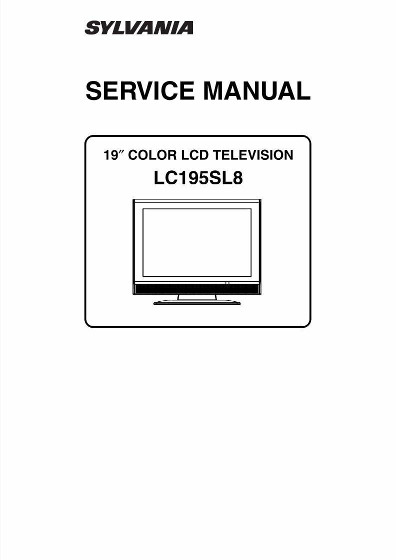
SERVICE MANUAL
19 ″ COLOR LCD TELEVISION
LC195SL8
7/21/2019 Sylvania Lc195sl8 Lcd Tv Sm
http://slidepdf.com/reader/full/sylvania-lc195sl8-lcd-tv-sm 2/60
IMPORTANT SAFETY NOTICE
Proper service and repair is important to the safe, reliable operation of allFunai Equipment. The service procedures recommended by Funai anddescribed in this service manual are effective methods of performingservice operations. Some of these service special tools should be used
when and as recommended.It is important to note that this service manual contains various CAUTIONSand NOTICES which should be carefully read in order to minimize the riskof personal injury to service personnel. The possibility exists that improperservice methods may damage the equipment. It also is important tounderstand that these CAUTIONS and NOTICES ARE NOT EXHAUSTIVE.Funai could not possibly know, evaluate and advice the service trade of allconceivable ways in which service might be done or of the possiblehazardous consequences of each way. Consequently, Funai has notundertaken any such broad evaluation. Accordingly, a servicer who uses aservice procedure or tool which is not recommended by Funai must firstuse all precautions thoroughly so that neither his safety nor the safeoperation of the equipment will be jeopardized by the service methodselected.
TABLE OF CONTENTSSpecifications . . . . . . . . . . . . . . . . . . . . . . . . . . . . . . . . . . . . . . . . . . . . . . . . . . . . . . . . . . . . . . . . . . . . . . . . . . . 1-1
Important Safety Precautions . . . . . . . . . . . . . . . . . . . . . . . . . . . . . . . . . . . . . . . . . . . . . . . . . . . . . . . . . . . . . . . 2-1Standard Notes for Servicing . . . . . . . . . . . . . . . . . . . . . . . . . . . . . . . . . . . . . . . . . . . . . . . . . . . . . . . . . . . . . . . 3-1Cabinet Disassembly Instructions. . . . . . . . . . . . . . . . . . . . . . . . . . . . . . . . . . . . . . . . . . . . . . . . . . . . . . . . . . . . 4-1Electrical Adjustment Instructions . . . . . . . . . . . . . . . . . . . . . . . . . . . . . . . . . . . . . . . . . . . . . . . . . . . . . . . . . . . . 5-1How to initialize the LCD Television . . . . . . . . . . . . . . . . . . . . . . . . . . . . . . . . . . . . . . . . . . . . . . . . . . . . . . . . . . 6-1Block Diagrams. . . . . . . . . . . . . . . . . . . . . . . . . . . . . . . . . . . . . . . . . . . . . . . . . . . . . . . . . . . . . . . . . . . . . . . . . . 7-1Schematic Diagrams / CBA’s and Test Points. . . . . . . . . . . . . . . . . . . . . . . . . . . . . . . . . . . . . . . . . . . . . . . . . . . 8-1Waveforms . . . . . . . . . . . . . . . . . . . . . . . . . . . . . . . . . . . . . . . . . . . . . . . . . . . . . . . . . . . . . . . . . . . . . . . . . . . . . 9-1Wiring Diagram . . . . . . . . . . . . . . . . . . . . . . . . . . . . . . . . . . . . . . . . . . . . . . . . . . . . . . . . . . . . . . . . . . . . . . . . . 10-1Exploded Views. . . . . . . . . . . . . . . . . . . . . . . . . . . . . . . . . . . . . . . . . . . . . . . . . . . . . . . . . . . . . . . . . . . . . . . . . 11-1Mechanical Parts List . . . . . . . . . . . . . . . . . . . . . . . . . . . . . . . . . . . . . . . . . . . . . . . . . . . . . . . . . . . . . . . . . . . . 12-1
Electrical Parts List . . . . . . . . . . . . . . . . . . . . . . . . . . . . . . . . . . . . . . . . . . . . . . . . . . . . . . . . . . . . . . . . . . . . . . 13-1
The LCD panel is manufactured to provide many years of useful life.Occasionally a few non active pixels may appear as a tiny spec of color.This is not to be considered a defect in the LCD screen.
7/21/2019 Sylvania Lc195sl8 Lcd Tv Sm
http://slidepdf.com/reader/full/sylvania-lc195sl8-lcd-tv-sm 3/601-1 A81N0SP
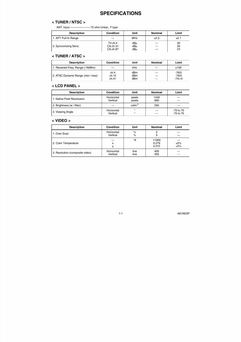
SPECIFICATIONS
< TUNER / NTSC >ANT. Input ---------------------- 75 ohm Unbal., F type
< TUNER / ATSC >
< LCD PANEL >
< VIDEO >
Description Condition Unit Nominal Limit
1. AFT Pull-In Range --- MHz ±2.3 ±2.1
2. Syncronizing Sens.TV.ch.4
CA.ch.31CA.ch.87
dBµdBµdBµ
---------
202023
Description Condition Unit Nominal Limit
1. Received Freq. Range (-28dBm) --- kHz --- ±100
2. ATSC Dynamic Range (min / max)ch.4ch.10ch.41
dBmdBmdBm
---------
-76/0-76/0-74/+4
Description Condition Unit Nominal Limit
1. Native Pixel Resolusion HorizontalVertical
pixelspixels
1440900
------
2. Brightness (w / filter) --- cd/m2 250 ---
3. Viewing Angle HorizontalVertical
°°
------
-75 to 75-70 to 70
Description Condition Unit Nominal Limit
1. Over Scan HorizontalVertical
%%
55
------
2. Color Temperature---xy
°K 110000.2790.272
---±5%±5%
3. Resolution (composite video) HorizontalVertical
lineline
400350
------
7/21/2019 Sylvania Lc195sl8 Lcd Tv Sm
http://slidepdf.com/reader/full/sylvania-lc195sl8-lcd-tv-sm 4/601-2 A81N0SP
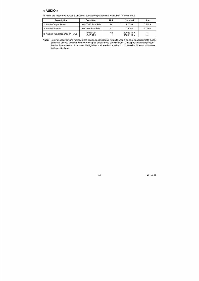
< AUDIO >All items are measured across 8Ω load at speaker output terminal with L.P.F. / Video1 Input.
Note: Nominal specifications represent the design specifications. All units should be able to approximate these.Some will exceed and some may drop slightly below these specifications. Limit specifications representthe absolute worst condition that still might be considered acceptable. In no case should a unit fail to meetlimit specifications.
Description Condition Unit Nominal Limit
1. Audio Output Power 10% THD: Lch/Rch W 1.0/1.0 0.9/0.92. Audio Distortion 500mW: Lch/Rch % 0.5/0.5 2.0/2.0
3. Audio Freq. Response (NTSC) -6dB: Lch
-6dB: RchHzHz
100 to 11 k100 to 11 k
------
7/21/2019 Sylvania Lc195sl8 Lcd Tv Sm
http://slidepdf.com/reader/full/sylvania-lc195sl8-lcd-tv-sm 5/602-1 LTVN_ISP
IMPORTANT SAFETY PRECAUTIONSPrior to shipment from the factory, our products are strictly inspected for recognized product safety and electricalcodes of the countries in which they are to be sold. However, in order to maintain such compliance, it is equallyimportant to implement the following precautions when a set is being serviced.
Safety Precautions for LCD TVCircuit1. Before returning an instrument to the
customer, always make a safety check of theentire instrument, including, but not limited to, thefollowing items:a. Be sure that no built-in protective devices are
defective and have been defeated duringservicing. (1) Protective shields are providedon this chassis to protect both the technicianand the customer. Correctly replace all missingprotective shields, including any removed forservicing convenience. (2) When reinstallingthe chassis and/or other assembly in thecabinet, be sure to put back in place allprotective devices, including but not limited to,nonmetallic control knobs, insulatingfishpapers, adjustment and compartmentcovers/shields, and isolation resistor/capacitornetworks.Do not operate this instrument orpermit it to be operated without allprotective devices correctly installed andfunctioning. Servicers who defeat safetyfeatures or fail to perform safety checksmay be liable for any resulting damage.
b. Be sure that there are no cabinet openings
through which an adult or child might be able toinsert their fingers and contact a hazardousvoltage. Such openings include, but are notlimited to, (1) spacing between the LiquidCrystal Panel and the cabinet mask, (2)excessively wide cabinet ventilation slots, and(3) an improperly fitted and/or incorrectlysecured cabinet back cover.
c. Antenna Cold Check - With the instrument ACplug removed from any AC source, connect anelectrical jumper across the two AC plugprongs. Place the instrument AC switch in theon position. Connect one lead of an ohmmeterto the AC plug prongs tied together and touchthe other ohmmeter lead in turn to each tunerantenna input exposed terminal screw and, ifapplicable, to the coaxial connector. If themeasured resistance is less than 1.0 megohmor greater than 5.2 megohm, an abnormalityexists that must be corrected before theinstrument is returned to the customer. Repeatthis test with the instrument AC switch in the offposition.
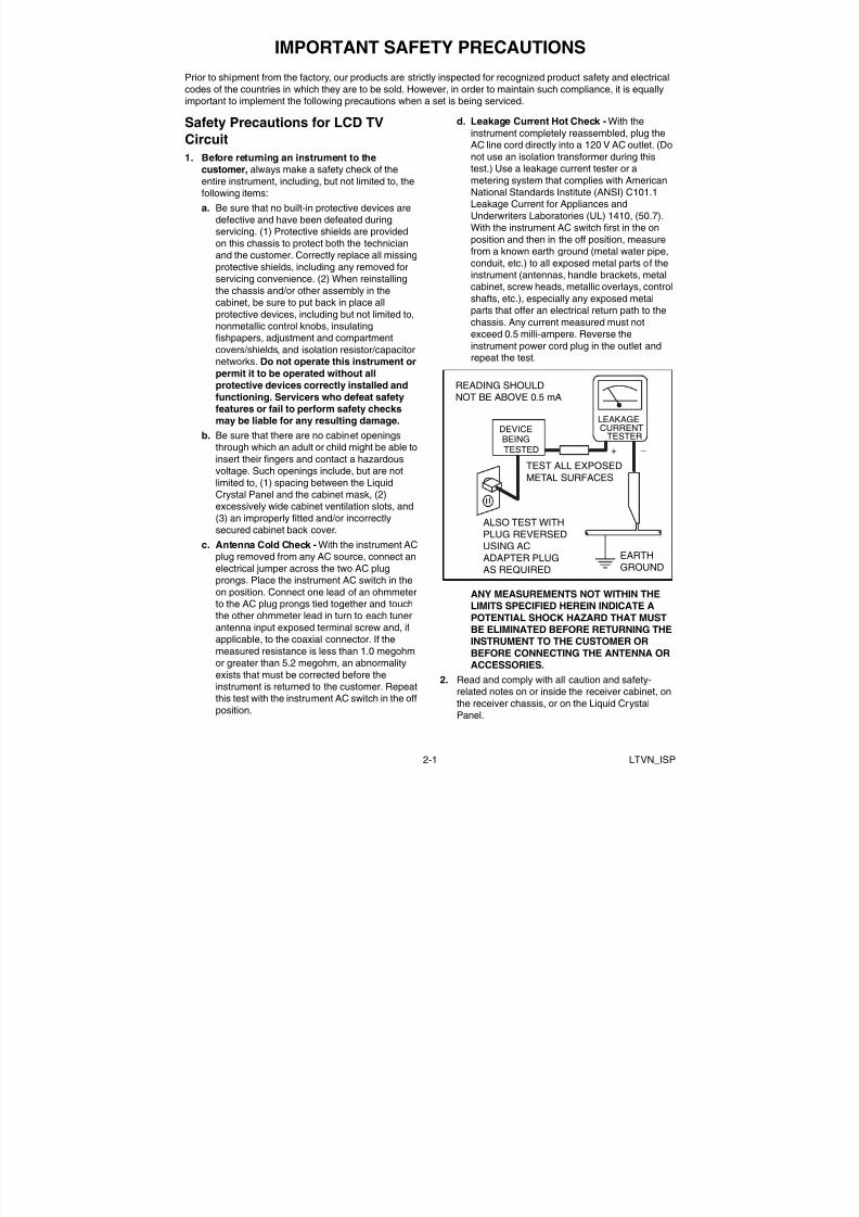
d. Leakage Current Hot Check - With theinstrument completely reassembled, plug the
AC line cord directly into a 120 V AC outlet. (Donot use an isolation transformer during thistest.) Use a leakage current tester or ametering system that complies with AmericanNational Standards Institute (ANSI) C101.1Leakage Current for Appliances andUnderwriters Laboratories (UL) 1410, (50.7).With the instrument AC switch first in the onposition and then in the off position, measurefrom a known earth ground (metal water pipe,conduit, etc.) to all exposed metal parts of theinstrument (antennas, handle brackets, metalcabinet, screw heads, metallic overlays, control
shafts, etc.), especially any exposed metalparts that offer an electrical return path to thechassis. Any current measured must notexceed 0.5 milli-ampere. Reverse theinstrument power cord plug in the outlet andrepeat the test.
ANY MEASUREMENTS NOT WITHIN THELIMITS SPECIFIED HEREIN INDICATE APOTENTIAL SHOCK HAZARD THAT MUSTBE ELIMINATED BEFORE RETURNING THEINSTRUMENT TO THE CUSTOMER ORBEFORE CONNECTING THE ANTENNA ORACCESSORIES.
2. Read and comply with all caution and safety-related notes on or inside the receiver cabinet, onthe receiver chassis, or on the Liquid CrystalPanel.
ALSO TEST WITHPLUG REVERSEDUSING ACADAPTER PLUGAS REQUIRED
TEST ALL EXPOSEDMETAL SURFACES
READING SHOULDNOT BE ABOVE 0.5 mA
EARTHGROUND
_
DEVICELEAKAGECURRENT
TESTER
+BEING
TESTED
7/21/2019 Sylvania Lc195sl8 Lcd Tv Sm
http://slidepdf.com/reader/full/sylvania-lc195sl8-lcd-tv-sm 6/602-2 LTVN_ISP
3. Design Alteration Warning - Do not alter or addto the mechanical or electrical design of this TVreceiver. Design alterations and additions,including, but not limited to circuit modificationsand the addition of items such as auxiliary audioand/or video output connections, might alter thesafety characteristics of this receiver and create ahazard to the user. Any design alterations oradditions will void the manufacturer's warranty andmay make you, the servicer, responsible forpersonal injury or property damage resultingtherefrom.
4. Hot Chassis Warning -a. Some TV receiver chassis are electrically
connected directly to one conductor of the ACpower cord and maybe safety-serviced withoutan isolation transformer only if the AC powerplug is inserted so that the chassis isconnected to the ground side of the AC powersource. To confirm that the AC power plug isinserted correctly, with an AC voltmeter,
measure between the chassis and a knownearth ground. If a voltage reading in excess of1.0 V is obtained, remove and reinsert the ACpower plug in the opposite polarity and againmeasure the voltage potential between thechassis and a known earth ground.
b. Some TV receiver chassis normally have 85VAC(RMS) between chassis and earth groundregardless of the AC plug polarity. This chassiscan be safety-serviced only with an isolationtransformer inserted in the power line betweenthe receiver and the AC power source, for bothpersonnel and test equipment protection.
c. Some TV receiver chassis have a secondaryground system in addition to the main chassisground. This secondary ground system is notisolated from the AC power line. The twoground systems are electrically separated byinsulation material that must not be defeated oraltered.
5. Observe original lead dress. Take extra care toassure correct lead dress in the following areas: a.near sharp edges, b. near thermally hot parts-besure that leads and components do not touchthermally hot parts, c. the AC supply, d. highvoltage, and, e. antenna wiring. Always inspect inall areas for pinched, out of place, or frayed wiring.Check AC power cord for damage.
6. Components, parts, and/or wiring that appear tohave overheated or are otherwise damagedshould be replaced with components, parts, orwiring that meet original specifications.Additionally, determine the cause of overheatingand/or damage and, if necessary, take correctiveaction to remove any potential safety hazard.
7. Product Safety Notice - Some electrical andmechanical parts have special safety-relatedcharacteristics which are often not evident fromvisual inspection, nor can the protection they givenecessarily be obtained by replacing them withcomponents rated for higher voltage, wattage, etc.Parts that have special safety characteristics areidentified by a# on schematics and in parts lists.Use of a substitute replacement that does nothave the same safety characteristics as therecommended replacement part might createshock, fire, and/or other hazards. The product'ssafety is under review continuously and newinstructions are issued whenever appropriate.Prior to shipment from the factory, our productsare strictly inspected to confirm they comply withthe recognized product safety and electrical codesof the countries in which they are to be sold.However, in order to maintain such compliance, itis equally important to implement the followingprecautions when a set is being serviced.
7/21/2019 Sylvania Lc195sl8 Lcd Tv Sm
http://slidepdf.com/reader/full/sylvania-lc195sl8-lcd-tv-sm 7/602-3 LTVN_ISP
Precautions during ServicingA. Parts identified by the# symbol are critical for
safety.Replace only with part number specified.
B. In addition to safety, other parts and assembliesare specified for conformance with regulationsapplying to spurious radiation. These must also bereplaced only with specified replacements.Examples: RF converters, RF cables, noiseblocking capacitors, and noise blocking filters, etc.
C. Use specified internal wiring. Note especially:1) Wires covered with PVC tubing2) Double insulated wires3) High voltage leads
D. Use specified insulating materials for hazardouslive parts. Note especially:1) Insulation Tape2) PVC tubing3) Spacers4) Insulators for transistors.
E. When replacing AC primary side components(transformers, power cord, etc.), wrap ends ofwires securely about the terminals beforesoldering.
F. Observe that the wires do not contact heatproducing parts (heat sinks, oxide metal filmresistors, fusible resistors, etc.)
G. Check that replaced wires do not contact sharpedged or pointed parts.
H. When a power cord has been replaced, check that
5~6 kg of force in any direction will not loosen it.I. Also check areas surrounding repaired locations.J. Use care that foreign objects (screws, solder
droplets, etc.) do not remain inside the set.K. When connecting or disconnecting the internal
connectors, first, disconnect the AC plug from theAC supply outlet.
L. When installing parts or assembling the cabinetparts, be sure to use the proper screws andtighten certainly.
7/21/2019 Sylvania Lc195sl8 Lcd Tv Sm
http://slidepdf.com/reader/full/sylvania-lc195sl8-lcd-tv-sm 8/602-4 LTVN_ISP
Safety Check after ServicingExamine the area surrounding the repaired location for damage or deterioration. Observe that screws, parts andwires have been returned to original positions. Afterwards, perform the following tests and confirm the specifiedvalues in order to verify compliance with safety standards.
1. Clearance DistanceWhen replacing primary circuit components, confirmspecified clearance distance (d) and (d') betweensoldered terminals, and between terminals andsurrounding metallic parts. (See Fig. 1)Table 1: Ratings for selected area
Note: This table is unofficial and for reference only. Besure to confirm the precise values.
2. Leakage Current TestConfirm the specified (or lower) leakage currentbetween B (earth ground, power cord plug prongs) andexternally exposed accessible parts (RF terminals,antenna terminals, video and audio input and outputterminals, microphone jacks, earphone jacks, etc.) islower than or equal to the specified value in the tablebelow.
Measuring Method: (Power ON)
Insert load Z between B (earth ground, power cord plugprongs) and exposed accessible parts. Use an ACvoltmeter to measure across both terminals of load Z.See Fig. 2 and following table.
Table 2: Leakage current ratings for selected areas
Note: This table is unofficial and for reference only. Be sure to confirm the precise values.
AC Line Voltage Region ClearanceDistance (d), (d’)
110 to 130 V U.S.A. orCanada
≥ 3.2 mm(0.126 inches)
AC Line Voltage Region Load Z Leakage Current (i) Earth Ground (B) to:
110 to 130 V U.S.A. orCanada
0.15 µF CAP. & 1.5 kΩ RES. Connected in parallel i ≤ 0.5 mA rms Exposed accessible
parts
Chassis or Secondary Conductor
Primary Circuit
Fig. 1
d' d
AC Voltmeter(High Impedance)
Exposed Accessible Part
B Earth GroundPower Cord Plug Prongs
Z
Fig. 2
7/21/2019 Sylvania Lc195sl8 Lcd Tv Sm
http://slidepdf.com/reader/full/sylvania-lc195sl8-lcd-tv-sm 9/603-1 TVN_SN
STANDARD NOTES FOR SERVICING
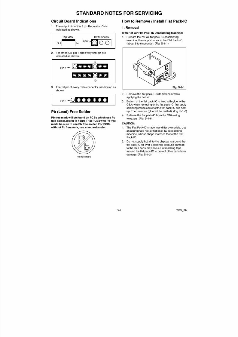
Circuit Board Indications1. The output pin of the 3 pin Regulator ICs is
indicated as shown.
2. For other ICs, pin 1 and every fifth pin areindicated as shown.
3. The 1st pin of every male connector is indicated asshown.
Pb (Lead) Free SolderPb free mark will be found on PCBs which use Pbfree solder. (Refer to figure.) For PCBs with Pb free
mark, be sure to use Pb free solder. For PCBswithout Pb free mark, use standard solder.
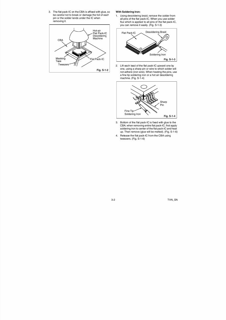
How to Remove / Install Flat Pack-IC
1. Removal
With Hot-Air Flat Pack-IC Desoldering Machine:1. Prepare the hot-air flat pack-IC desoldering
machine, then apply hot air to the Flat Pack-IC(about 5 to 6 seconds). (Fig. S-1-1)
2. Remove the flat pack-IC with tweezers whileapplying the hot air.
3. Bottom of the flat pack-IC is fixed with glue to theCBA; when removing entire flat pack-IC, first applysoldering iron to center of the flat pack-IC and heatup. Then remove (glue will be melted). (Fig. S-1-6)
4. Release the flat pack-IC from the CBA usingtweezers. (Fig. S-1-6)
CAUTION:1. The Flat Pack-IC shape may differ by models. Usean appropriate hot-air flat pack-IC desolderingmachine, whose shape matches that of the FlatPack-IC.
2. Do not supply hot air to the chip parts around theflat pack-IC for over 6 seconds because damageto the chip parts may occur. Put masking tapearound the flat pack-IC to protect other parts fromdamage. (Fig. S-1-2)
Top View
Out In
Bottom View
Input
5
10
Pin 1
Pin 1
Pb free mark
Fig. S-1-1
7/21/2019 Sylvania Lc195sl8 Lcd Tv Sm
http://slidepdf.com/reader/full/sylvania-lc195sl8-lcd-tv-sm 10/603-2 TVN_SN
3. The flat pack-IC on the CBA is affixed with glue, sobe careful not to break or damage the foil of eachpin or the solder lands under the IC whenremoving it.
With Soldering Iron:1. Using desoldering braid, remove the solder from
all pins of the flat pack-IC. When you use solderflux which is applied to all pins of the flat pack-IC,you can remove it easily. (Fig. S-1-3)
2. Lift each lead of the flat pack-IC upward one byone, using a sharp pin or wire to which solder willnot adhere (iron wire). When heating the pins, usea fine tip soldering iron or a hot air desoldering
machine. (Fig. S-1-4)
3. Bottom of the flat pack-IC is fixed with glue to theCBA; when removing entire flat pack-IC, first applysoldering iron to center of the flat pack-IC and heatup. Then remove (glue will be melted). (Fig. S-1-6)
4. Release the flat pack-IC from the CBA usingtweezers. (Fig. S-1-6)
Hot-airFlat Pack-ICDesoldering
MachineCBA
Flat Pack-IC
Tweezers
MaskingTape
Fig. S-1-2
Flat Pack-IC Desoldering Braid
Soldering Iron
Fig. S-1-3
Fine TipSoldering Iron
SharpPin
Fig. S-1-4
7/21/2019 Sylvania Lc195sl8 Lcd Tv Sm
http://slidepdf.com/reader/full/sylvania-lc195sl8-lcd-tv-sm 11/603-3 TVN_SN
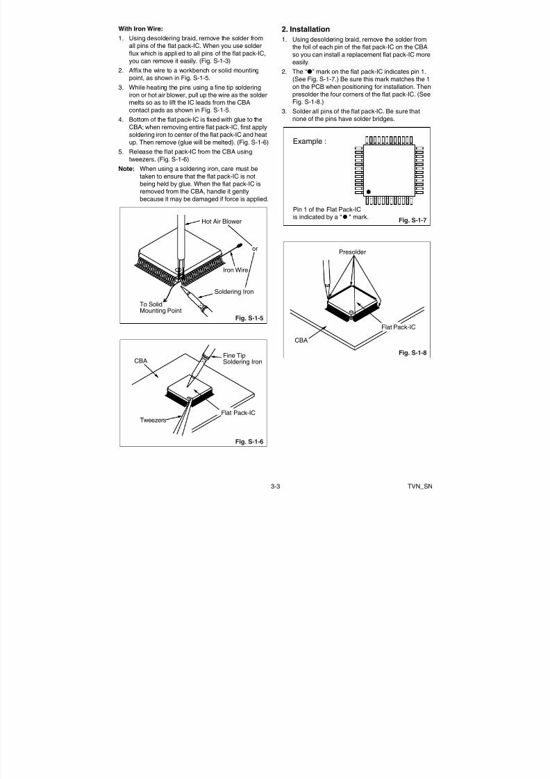
With Iron Wire:1. Using desoldering braid, remove the solder from
all pins of the flat pack-IC. When you use solderflux which is applied to all pins of the flat pack-IC,you can remove it easily. (Fig. S-1-3)
2. Affix the wire to a workbench or solid mountingpoint, as shown in Fig. S-1-5.
3. While heating the pins using a fine tip soldering
iron or hot air blower, pull up the wire as the soldermelts so as to lift the IC leads from the CBAcontact pads as shown in Fig. S-1-5.
4. Bottom of the flat pack-IC is fixed with glue to theCBA; when removing entire flat pack-IC, first applysoldering iron to center of the flat pack-IC and heatup. Then remove (glue will be melted). (Fig. S-1-6)
5. Release the flat pack-IC from the CBA usingtweezers. (Fig. S-1-6)
Note: When using a soldering iron, care must betaken to ensure that the flat pack-IC is notbeing held by glue. When the flat pack-IC is
removed from the CBA, handle it gentlybecause it may be damaged if force is applied.
2. Installation1. Using desoldering braid, remove the solder from
the foil of each pin of the flat pack-IC on the CBAso you can install a replacement flat pack-IC moreeasily.
2. The “ ” mark on the flat pack-IC indicates pin 1.(See Fig. S-1-7.) Be sure this mark matches the 1on the PCB when positioning for installation. Then
presolder the four corners of the flat pack-IC. (SeeFig. S-1-8.)3. Solder all pins of the flat pack-IC. Be sure that
none of the pins have solder bridges.
To SolidMounting Point
Soldering Iron
Iron Wire
or
Hot Air Blower
Fig. S-1-5
Fine TipSoldering IronCBA
Flat Pack-ICTweezers
Fig. S-1-6
Example :
Pin 1 of the Flat Pack-ICis indicated by a " " mark. Fig. S-1-7
Presolder
CBA
Flat Pack-IC
Fig. S-1-8
7/21/2019 Sylvania Lc195sl8 Lcd Tv Sm
http://slidepdf.com/reader/full/sylvania-lc195sl8-lcd-tv-sm 12/603-4 TVN_SN
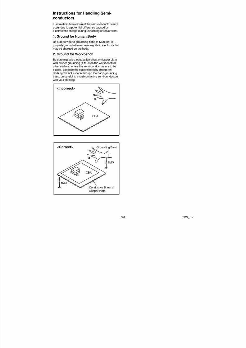
Instructions for Handling Semi-conductorsElectrostatic breakdown of the semi-conductors mayoccur due to a potential difference caused byelectrostatic charge during unpacking or repair work.
1. Ground for Human Body
Be sure to wear a grounding band (1 MΩ) that isproperly grounded to remove any static electricity thatmay be charged on the body.
2. Ground for WorkbenchBe sure to place a conductive sheet or copper platewith proper grounding (1 MΩ) on the workbench orother surface, where the semi-conductors are to beplaced. Because the static electricity charge onclothing will not escape through the body groundingband, be careful to avoid contacting semi-conductorswith your clothing.
<Incorrect>
CBA
Grounding Band
Conductive Sheet orCopper Plate
1MΩ
1MΩ
<Correct>
CBA
7/21/2019 Sylvania Lc195sl8 Lcd Tv Sm
http://slidepdf.com/reader/full/sylvania-lc195sl8-lcd-tv-sm 13/604-1 A81N2DC
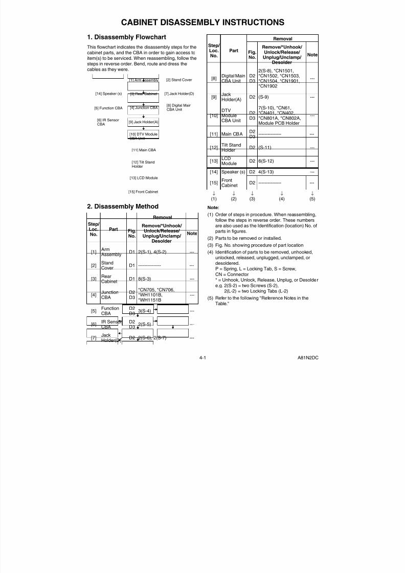
CABINET DISASSEMBLY INSTRUCTIONS
1. Disassembly FlowchartThis flowchart indicates the disassembly steps for thecabinet parts, and the CBA in order to gain access toitem(s) to be serviced. When reassembling, follow thesteps in reverse order. Bend, route and dress the
cables as they were.
2. Disassembly Method Note:
(1) Order of steps in procedure. When reassembling,follow the steps in reverse order. These numbersare also used as the Identification (location) No. ofparts in figures.
(2) Parts to be removed or installed.(3) Fig. No. showing procedure of part location(4) Identification of parts to be removed, unhooked,
unlocked, released, unplugged, unclamped, ordesoldered.P = Spring, L = Locking Tab, S = Screw,CN = Connector* = Unhook, Unlock, Release, Unplug, or Desoldere.g. 2(S-2) = two Screws (S-2), 2(L-2) = two Locking Tabs (L-2)
(5) Refer to the following "Reference Notes in theTable."
Step/ Loc.No.
Part
Removal
Fig.No.
Remove/*Unhook/ Unlock/Release/
Unplug/Unclamp/ Desolder
Note
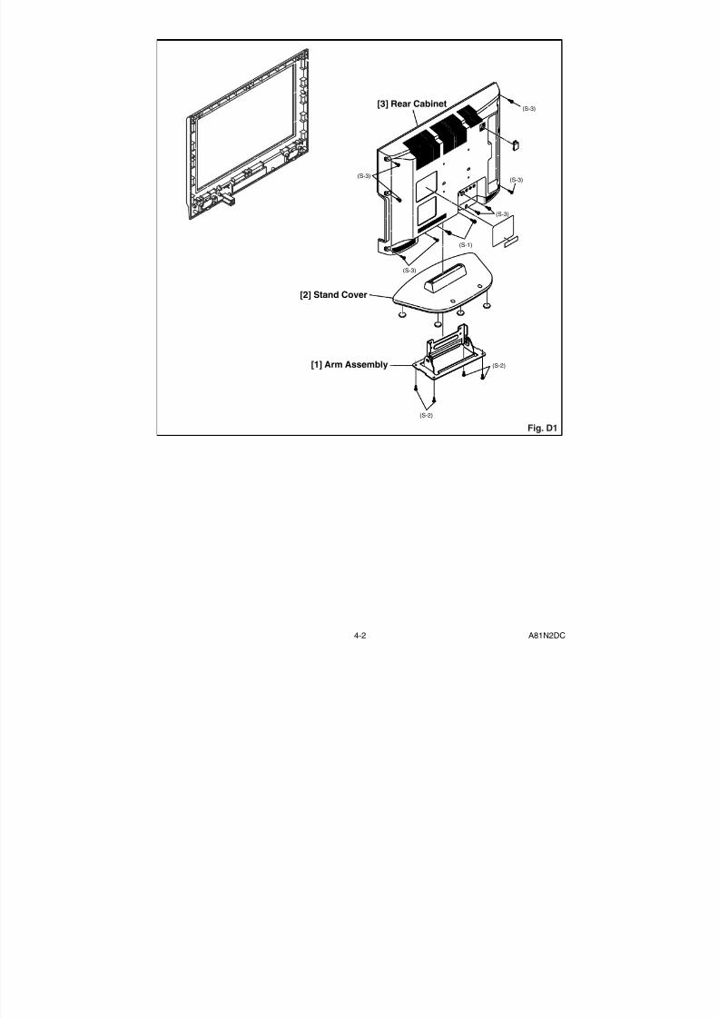
[1] ArmAssembly D1 2(S-1), 4(S-2) ---
[2] StandCover D1 --------------- ---
[3] Rear
CabinetD1 8(S-3) ---
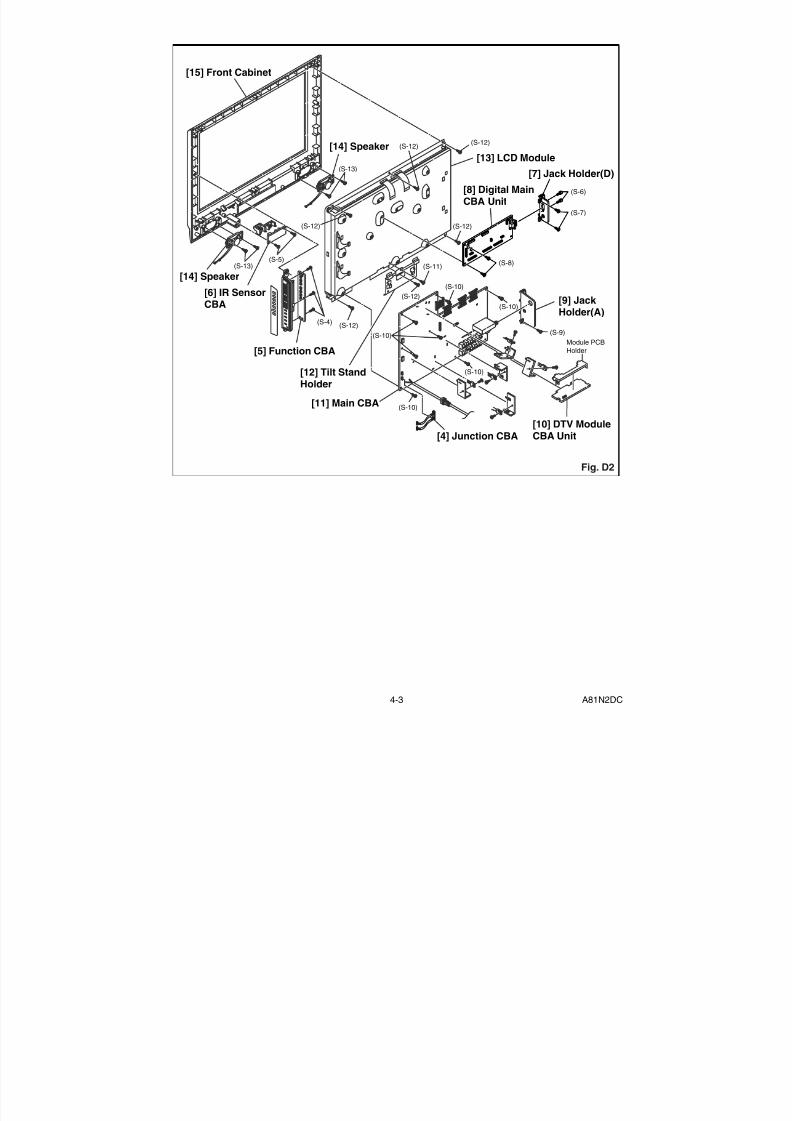
[4] JunctionCBA
D2D3
*CN705, *CN706,*WH1101B,*WH1151B
---
[5] FunctionCBA
D2D3 3(S-4) ---
[6] IR SensorCBA
D2D3 2(S-5) ---
[7] JackHolder(D) D2 2(S-6), 2(S-7) ---
[2] Stand Cover
[7] Jack Holder(D)[3] Rear Cabinet
[1] Arm Assembly
[14] Speaker (s)
[4] Junction CBA
[9] Jack Holder(A)
[10] DTV ModuleCBA Unit
[6] IR SensorCBA
[5] Function CBA
[11] Main CBA
[12] Tilt StandHolder
[8] Digital MainCBA Unit
[13] LCD Module
[15] Front Cabinet
[8] Digital MainCBA Unit
D2D3
2(S-8), *CN1501,*CN1502, *CN1503,*CN1504, *CN1901,*CN1902
---
[9] JackHolder(A) D2 (S-9) ---
[10]DTVModuleCBA Unit
D2D3
7(S-10), *CN61,*CN401, *CN402,*CN801A, *CN802A,Module PCB Holder
---
[11] Main CBA D2D3 --------------- ---
[12] Tilt StandHolder D2 (S-11) ---
[13] LCDModule D2 6(S-12) ---
[14] Speaker (s) D2 4(S-13) ---
[15] FrontCabinet D2 --------------- ---
↓(1)
↓(2)
↓(3)
↓(4)
↓(5)
Step/ Loc.No.
Part
Removal
Fig.No.
Remove/*Unhook/ Unlock/Release/
Unplug/Unclamp/ Desolder
Note
7/21/2019 Sylvania Lc195sl8 Lcd Tv Sm
http://slidepdf.com/reader/full/sylvania-lc195sl8-lcd-tv-sm 14/604-2 A81N2DC
Fig. D1
[3] Rear Cabinet
(S-1)
(S-3)
[1] Arm Assembly
[2] Stand Cover
(S-2)
(S-3)
(S-3)
(S-3)
(S-3)
(S-2)
7/21/2019 Sylvania Lc195sl8 Lcd Tv Sm
http://slidepdf.com/reader/full/sylvania-lc195sl8-lcd-tv-sm 15/604-3 A81N2DC
[9] Jack Holder(A)
[7] Jack Holder(D)
[5] Function CBA
[6] IR SensorCBA
[15] Front Cabinet
[14] Speaker
[14] Speaker
[12] Tilt StandHolder
(S-9)
(S-11)
[11] Main CBA
(S-7)
(S-6)
[10] DTV ModuleCBA Unit
Module PCBHolder
[13] LCD Module
(S-12)
(S-8)
(S-10)
(S-10)
(S-10)
(S-12)
(S-12)(S-12)
(S-12)
(S-12)
(S-4)
(S-10)
(S-10)
[8] Digital MainCBA Unit
(S-5)(S-13)
(S-13)
[4] Junction CBA
Fig. D2
7/21/2019 Sylvania Lc195sl8 Lcd Tv Sm
http://slidepdf.com/reader/full/sylvania-lc195sl8-lcd-tv-sm 16/604-4 A81N2DC
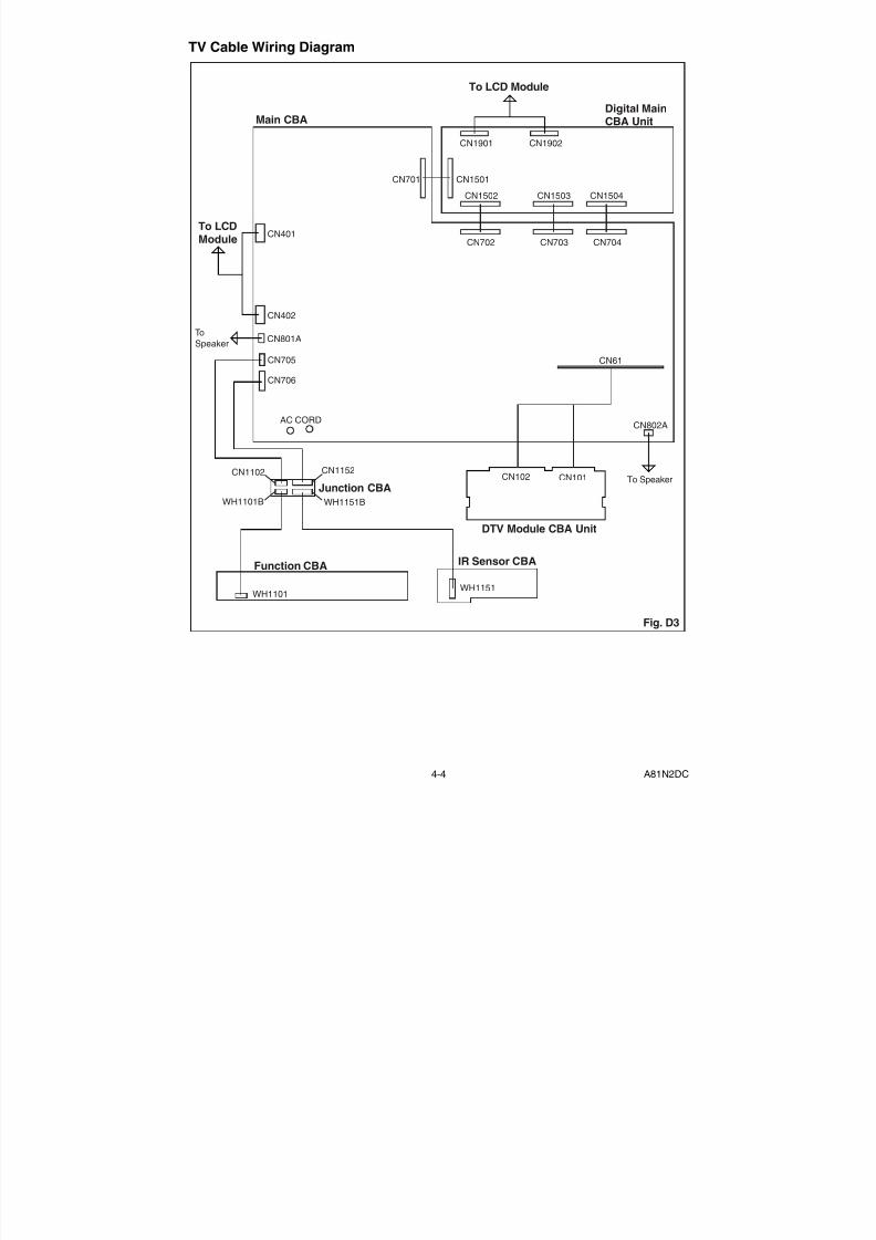
TV Cable Wiring Diagram
Main CBA
CN701 CN1501
CN702 CN703 CN704
CN1502 CN1503 CN1504
CN1901 CN1902
Digital MainCBA Unit
To LCD Module
CN61
To Speaker
DTV Module CBA Unit
CN101CN102
CN802AAC CORD
CN401
CN402
To LCDModule
ToSpeaker CN801A
CN705
CN706
CN1102 CN1152
WH1101B WH1151BJunction CBA
WH1101
Function CBA
WH1151
IR Sensor CBA
Fig. D3
7/21/2019 Sylvania Lc195sl8 Lcd Tv Sm
http://slidepdf.com/reader/full/sylvania-lc195sl8-lcd-tv-sm 17/605-1 A81N2EA
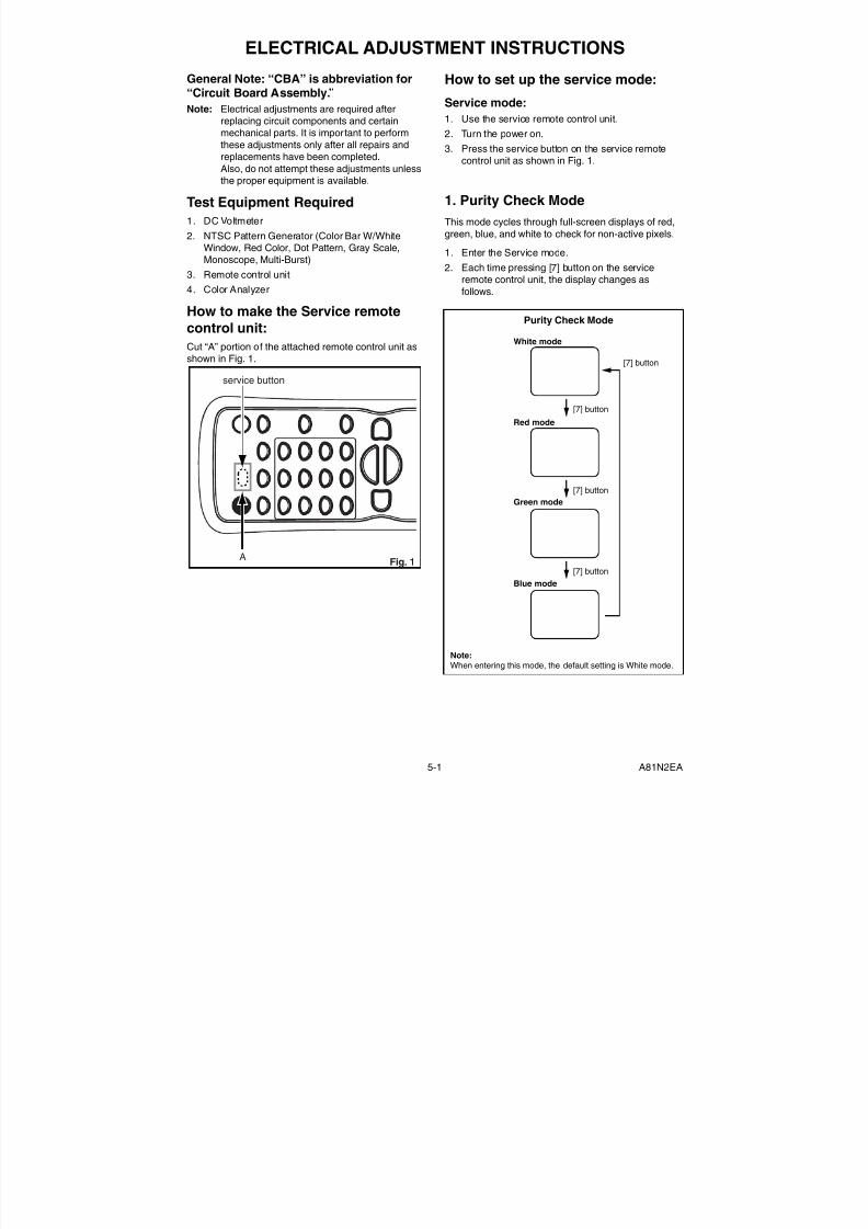
ELECTRICAL ADJUSTMENT INSTRUCTIONS
General Note: “CBA” is abbreviation for“Circuit Board Assembly.”Note: Electrical adjustments are required after
replacing circuit components and certainmechanical parts. It is important to performthese adjustments only after all repairs andreplacements have been completed.Also, do not attempt these adjustments unlessthe proper equipment is available.
Test Equipment Required1. DC Voltmeter2. NTSC Pattern Generator (Color Bar W/White
Window, Red Color, Dot Pattern, Gray Scale,Monoscope, Multi-Burst)
3. Remote control unit4. Color Analyzer
How to make the Service remotecontrol unit:Cut “A” portion of the attached remote control unit asshown in Fig. 1.
How to set up the service mode:
Service mode:1. Use the service remote control unit.2. Turn the power on.
3. Press the service button on the service remotecontrol unit as shown in Fig. 1.
1. Purity Check ModeThis mode cycles through full-screen displays of red,green, blue, and white to check for non-active pixels.
1. Enter the Service mode.2. Each time pressing [7] button on the service
remote control unit, the display changes asfollows.
Fig. 1
service button
A
[7] button
Note:When entering this mode, the default setting is White mode.
Purity Check Mode
[7] buttonRed mode
Green mode
Blue mode
White mode
[7] button
[7] button
7/21/2019 Sylvania Lc195sl8 Lcd Tv Sm
http://slidepdf.com/reader/full/sylvania-lc195sl8-lcd-tv-sm 18/605-2 A81N2EA
2. Auto Calibration [Component]Purpose: To bring the color adjustment of eachcomponent into standard alignment.Symptom of Misadjustment: If this adjustment isincorrect, component signals do not reproduce thecorresponding color.1. Input 1080i 100% Color Bar signal.2. Enter the service mode.3. To enter the Auto Calibration adjustment mode,
press [6] button on service the remote control unit.4. To start auto adjustment, press [1] button on the
service remote control unit.- In the auto adjustment mode, “Please wait”
appears on the screen.- Upon completion, “OK” appears on the screen.
3. Auto Calibration [DTV]Purpose: To bring the color adjustment of DTV intostandard alignment.Symptom of Misadjustment: If this adjustment isincorrect, DTV signals do not reproduce thecorresponding color.1. Enter the service mode.2. To enter the Auto Calibration adjustment mode,
press [6] button on the service remote control unit.3. To start auto adjustment, press [2] button on the
service remote control unit.- In the auto adjustment mode, “Please wait”
appears on the screen.- Upon completion, “OK” appears on the screen.
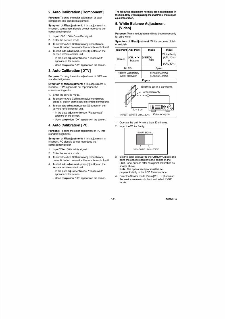
4. Auto Calibration [PC]Purpose: To bring the color adjustment of PC intostandard alignment.Symptom of Misadjustment: If this adjustment isincorrect, PC signals do not reproduce thecorresponding color.1. Input XGA 100% White signal.2. Enter the service mode.
3. To enter the Auto Calibration adjustment mode,press [6] button on service the remote control unit.4. To start auto adjustment, press [3] button on the
service remote control unit.- In the auto adjustment mode, “Please wait”
appears on the screen.- Upon completion, “OK” appears on the screen.
The following adjustment normally are not attempted inthe field. Only when replacing the LCD Panel then adjustas a preparation.
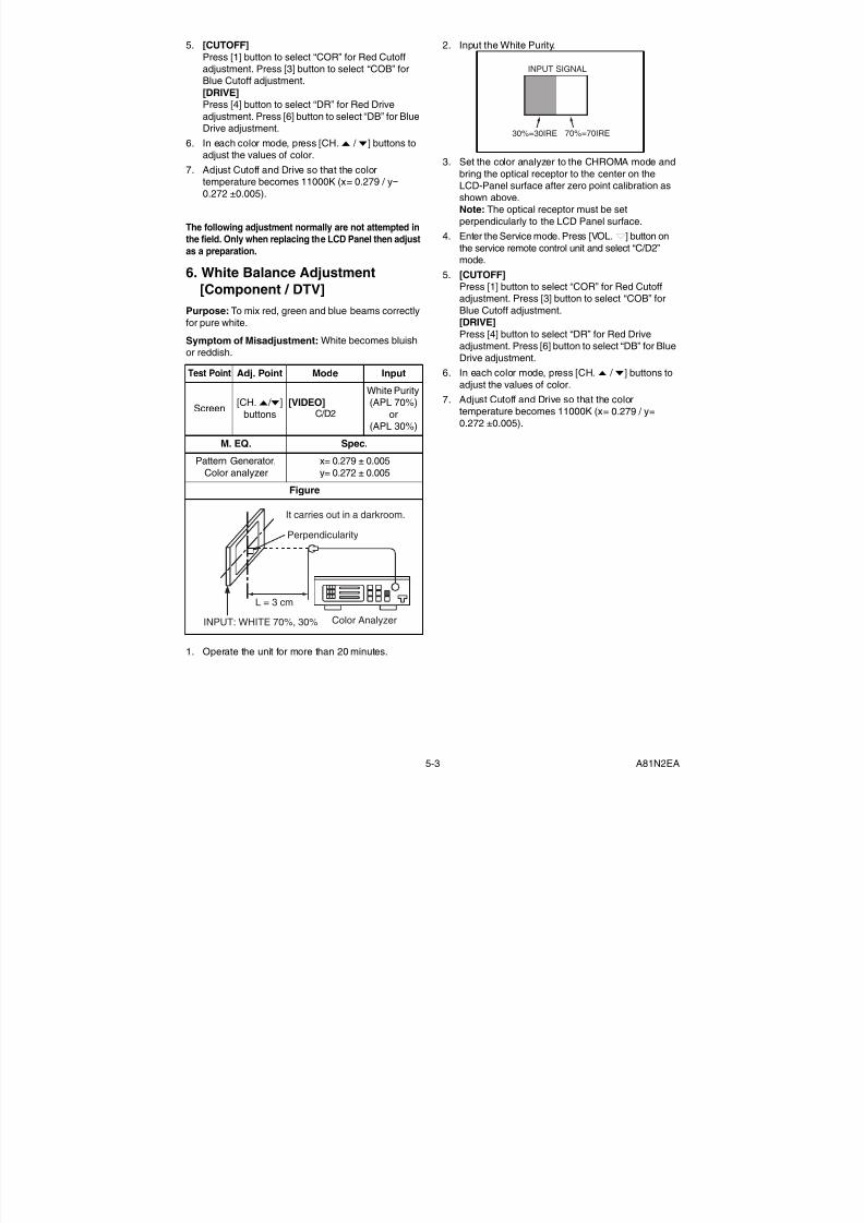
5. White Balance Adjustment[Video]
Purpose: To mix red, green and blue beams correctlyfor pure white.Symptom of Misadjustment: White becomes bluishor reddish.
1. Operate the unit for more than 20 minutes.2. Input the White Purity.
3. Set the color analyzer to the CHROMA mode andbring the optical receptor to the center on theLCD-Panel surface after zero point calibration asshown above.Note: The optical receptor must be setperpendicularly to the LCD Panel surface.
4. Enter the Service mode. Press [VOL. n ] button onthe service remote control unit and select “C/D1”mode.
Test Point Adj. Point Mode Input
Screen [CH.o / p ]buttons
[VIDEO]C/D1
White Purity(APL 70%)
or(APL 30%)
M. EQ. Spec.
Pattern Generator,Color analyzer
x= 0.279 ± 0.005y= 0.272 ± 0.005
Figure
Color Analyzer
It carries out in a darkroom.
L = 3 cm
Perpendicularity
INPUT: WHITE 70%, 30%
30%=30IRE 70%=70IRE
INPUT SIGNAL
7/21/2019 Sylvania Lc195sl8 Lcd Tv Sm
http://slidepdf.com/reader/full/sylvania-lc195sl8-lcd-tv-sm 19/605-3 A81N2EA
5. [CUTOFF]Press [1] button to select “COR” for Red Cutoffadjustment. Press [3] button to select “COB” forBlue Cutoff adjustment.[DRIVE]Press [4] button to select “DR” for Red Driveadjustment. Press [6] button to select “DB” for BlueDrive adjustment.
6. In each color mode, press [CH.o / p ] buttons toadjust the values of color.
7. Adjust Cutoff and Drive so that the colortemperature becomes 11000K (x= 0.279 / y=0.272 ±0.005).
The following adjustment normally are not attempted inthe field. Only when replacing the LCD Panel then adjustas a preparation.
6. White Balance Adjustment[Component / DTV]
Purpose: To mix red, green and blue beams correctlyfor pure white.Symptom of Misadjustment: White becomes bluishor reddish.
1. Operate the unit for more than 20 minutes.
2. Input the White Purity.
3. Set the color analyzer to the CHROMA mode andbring the optical receptor to the center on theLCD-Panel surface after zero point calibration asshown above.Note: The optical receptor must be setperpendicularly to the LCD Panel surface.
4. Enter the Service mode. Press [VOL. n ] button onthe service remote control unit and select “C/D2”mode.
5. [CUTOFF]Press [1] button to select “COR” for Red Cutoff
adjustment. Press [3] button to select “COB” forBlue Cutoff adjustment.[DRIVE]Press [4] button to select “DR” for Red Driveadjustment. Press [6] button to select “DB” for BlueDrive adjustment.
6. In each color mode, press [CH.o / p ] buttons toadjust the values of color.
7. Adjust Cutoff and Drive so that the colortemperature becomes 11000K (x= 0.279 / y=0.272 ±0.005).
Test Point Adj. Point Mode Input
Screen [CH.o / p ]buttons
[VIDEO]C/D2
White Purity(APL 70%)
or(APL 30%)
M. EQ. Spec.
Pattern Generator,Color analyzer
x= 0.279 ± 0.005y= 0.272 ± 0.005
Figure
Color Analyzer
It carries out in a darkroom.
L = 3 cm
Perpendicularity
INPUT: WHITE 70%, 30%
30%=30IRE 70%=70IRE
INPUT SIGNAL

7/21/2019 Sylvania Lc195sl8 Lcd Tv Sm
http://slidepdf.com/reader/full/sylvania-lc195sl8-lcd-tv-sm 20/606-1 A81N0INT
HOW TO INITIALIZE THE LCD TELEVISION
How to initialize the LCD television:1. Turn the power on.2. To enter the service mode, press the service
button on the service remote control unit. (Refer topage 5-1.)
- To cancel the service mode, press [POWER]button on the service remote control unit.
3. Press [DISPLAY] button on the service remotecontrol unit to initialize the LCD television.
4. "FF" will appear in the upper left of the screen."FF" color will change to red from white wheninitialzing is complete.
7/21/2019 Sylvania Lc195sl8 Lcd Tv Sm
http://slidepdf.com/reader/full/sylvania-lc195sl8-lcd-tv-sm 21/60
7/21/2019 Sylvania Lc195sl8 Lcd Tv Sm
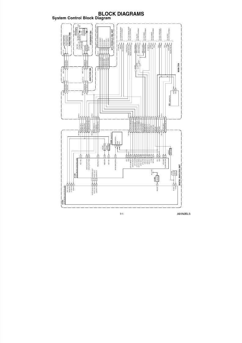
http://slidepdf.com/reader/full/sylvania-lc195sl8-lcd-tv-sm 22/607-2 A81N2BLIF
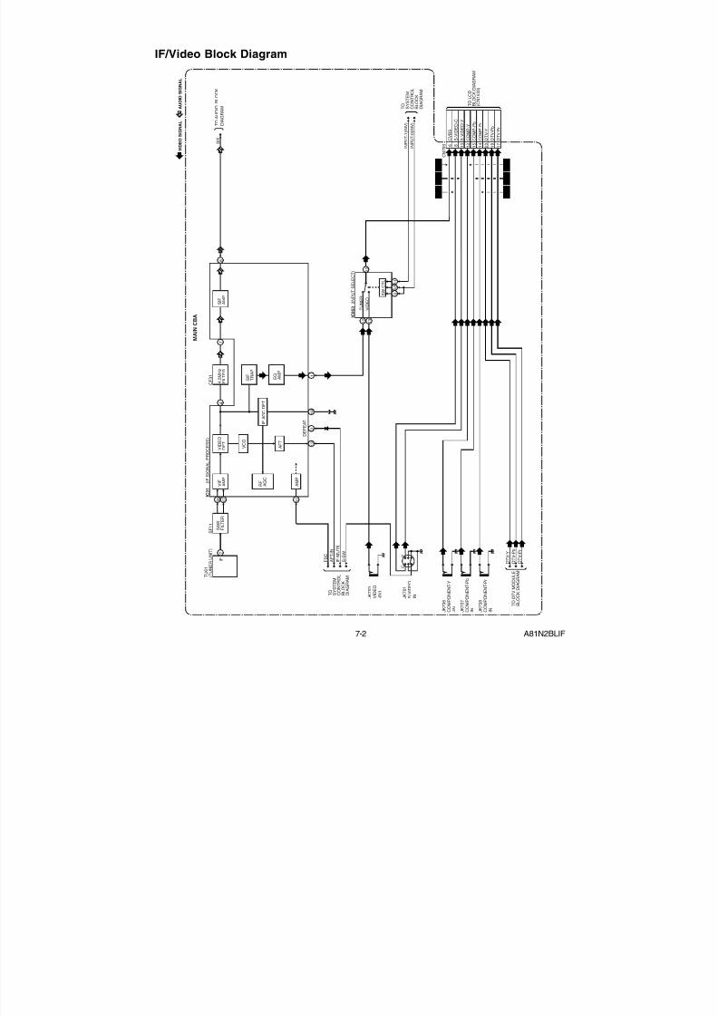
IF/Video Block Diagram
S A W
F I L T E R
T U 6 1
S F 1 1
I F 7
S I F
M A I N C B A
T O A U D I O B L O C K
D
I A G R A M
J K 7 0 6
C O M P O N E N T - Y
- I N J K 7 0 7
C O M P O N E N T - P b
I N J K 7 0 8
C O M P O N E N T - P r
I N
J K 7 0 3
V I D E O
- I N 1
J K 7 0 1
S - V
I D E O
I N T O S Y S T E M
C O N T R O L
B L O C K
D I A G R A M
S - S
W
I F - M U T E
A F T - I N
C
Y
( T U N E R U N I T )
C F 3 1
I C 3 1
( I F S I G N A L P R O C E S S )
V I F
A M P
V I D E O
D E T
V C O
4 . 5 M
H z
F I L T E R
R F
A G C
A M P
S I F
A M P
1 6
1 3
1 8
1 7
4
7
8
1 S I F T R A P
1 1
F S C
D T V - Y
T O D T V M O D U L E
B L O C K D I A G R A M
I F A G C D E T
A F T
E Q A M
P
2 D E F E A T
C N 7 0 3
T O L C D
B L O C K D I A G R A M
( C N 1 5 0 3 )
V I D E O S I G N A L
A U D I O S I G N A L
C V B S
6 S - V
I D E O - C
8 S - V
I D E O - Y
1 0 C O M P - Y
1 2 C O M P - P b
1 5 C O M P - P r
1 4 D T V - Y
2 0 D T V - P b
1 8 D T V - P r
1 7
D T V - P b
D T V - P r
W F 1
W F 2
W F 3
W F 4
W F 5
W F 6
I C 8 5 3 ( I N P U T S E L E C T )
S W
C T L
1 2
9 1 0 1 1
T U N E R
1 4
V I D E O
1 3
I N P U T - 1 ( I N V )
I N P U T - 0 ( I N V )
T O S Y S T E M
C O N T R O L
B L O C K
D I A G R A M
7/21/2019 Sylvania Lc195sl8 Lcd Tv Sm
http://slidepdf.com/reader/full/sylvania-lc195sl8-lcd-tv-sm 23/60
7/21/2019 Sylvania Lc195sl8 Lcd Tv Sm
http://slidepdf.com/reader/full/sylvania-lc195sl8-lcd-tv-sm 24/607-4
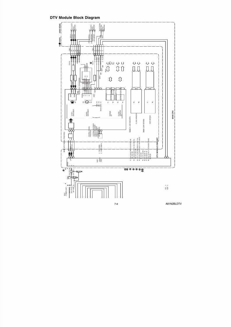
DTV Module Block Diagram
A81N2BLDTV
I C 1 0 1 ( D T V S I G N A L P R O C E S S )
I C 2 5 2
( A U D I O D / A C O N V E R T E R )
I C 2 0 2 ( F L A S H M E M O R Y )
A D C
/ A G C I / F
D I G I T A L S I G N A L
P R O C E S S
S Y S T E M D E C O D E R
/ V I D E O D E C O D E R
/ V I D E O F O R M A T
C O N V E R T E R
/ 2 D G R A P H I C S
T U 6 1
( T U N E R U N I T )
D I F - O U T 1
C N 6 1
C N 1 0 2
L P F
D I F - O U T 2
D I F - A G C
S D A
S C L
D T V M O D U L E C B A U N I T
M A I N C B A
V I D E O S I G N A L
2 6
1 1
D I F - O
U T 1
2 7
1 2
D I F - O
U T 2
2 4
9
D I F - A
G C
1 8
3 3
D T V - Y
1 9
3 4
D T V - P r
2 0
3 5
D T V - P b
1 5
3 0
D T V - A U D I O ( L )
1 6
3 1
D T V - A U D I O ( R )
1 0 1 1 8
1 7 4
1 7 8
1 8 2
1 8 7
1 8 6
1 5 9
1 5 8
1 6 2
1 6 1
6 5
1 5 1 4
7 8
1 5 6
1 4 4
1 4 3
1 4 0
4 1
X I N - 2 5 M
H z
X O U T - 2 5 M H z
2 5 M H z
O
S C
X 2 8 1
4 5
V I D E O
E N C O D E R
A U D I O
D E C O D E R
A U D I O
D / A
C O N V E R T E R
S D R A M
I / F F L A S H
M E M O R Y
I / F
I C 2 0 1 ( D D R S D R A M )
2
2
D T V - S P D I F
1 4
1 4
S D A
1 5
1 5
S C L
4 5
5
5
T U - S
D A
4
4
T U - S
C L
C N 6 1
L - C
H
R - C
H
S D A
S C L
B U S - C
O N T
* 1
* 1 7 9 ~ 8 1 , 8 5 , 8 7 , 8 9 ~ 9 1 , 9 2 , 9 4 , 9 6 ~ 9 8 ,
1 0 2 , 1 0 4 , 1 0 6
* 2
* 2 5 5 , 5 6 , 5 8 , 6 0 , 6 1 , 1 1 6 , 1 1 9 , 1 2 0 , 1 2 4 ,
1 2 5 , 1 2 7 , 1 2 9 , 1 3 0
* 3
* 3 1 , 2 , 7 ~ 1 2 , 2 0 , 2 0 6 , 2 0 9 , 2 1 1 , 2 1 3 ~ 2 1 6 ,
* 4
* 4 2 3 ~ 2 5 , 2 7 , 2 9 , 3 2 ~ 3 6 , 4 1 ~ 4 4 , 4 7 , 4 8 , 5 0 ,
5 2 ~ 5 4 , 2 0 5
* 5
* 5 1 ~ 9 , 1 6 ~ 2 5 , 4 8
* 6
* 6 2 9 ~ 3 6 , 3 8 ~ 4 5
* 7
* 7 2 8 ~ 3 2 , 3 5 ~ 4 2
* 8
* 8 2 , 4 , 5 , 7 , 8 , 1 0 , 1 1 , 1 3 , 5 4 , 5 6 , 5 7 , 5 9 , 6 0 ,
6 2 , 6 3 , 6 5
T O I F / V I D E O
B L O C K
D I A G R A M
T O A U D I O
B L O C K
D I A G R A M
T O S Y S T E M
C O N T R O L
B L O C K
D I A G R A M
C N 6 1
C N 1 0 1
B U F F E R
Q 2 4 3
B U F F E R
Q 2 4 5
B U F F E R
Q 2 4 4
B U F F E R
Q 2 5 1
S D A
S C L
D A T A B U S ( 0 - 1 5 )
A D D R E S S B U S ( 0 - 1 2 )
D A T A B U S ( 0 - 1 5 )
A D D R E S S B U S ( 1 - 2 0 )
C N 1 0 2
D D R S D R A M
F L A S
H M E M O R Y
S W
S W
D T V - S P D I F
D T V - A U D I O ( L )
D T V - A U D I O ( R )
D T V - P b
D T V - P r
D T V - Y
Q 2 1 1
Q 2 1 2
Q 2 1 3
Q 2 1 4
A U D I O S I G N A L
7/21/2019 Sylvania Lc195sl8 Lcd Tv Sm
http://slidepdf.com/reader/full/sylvania-lc195sl8-lcd-tv-sm 25/60
7/21/2019 Sylvania Lc195sl8 Lcd Tv Sm
http://slidepdf.com/reader/full/sylvania-lc195sl8-lcd-tv-sm 26/60
7/21/2019 Sylvania Lc195sl8 Lcd Tv Sm
http://slidepdf.com/reader/full/sylvania-lc195sl8-lcd-tv-sm 27/607-7
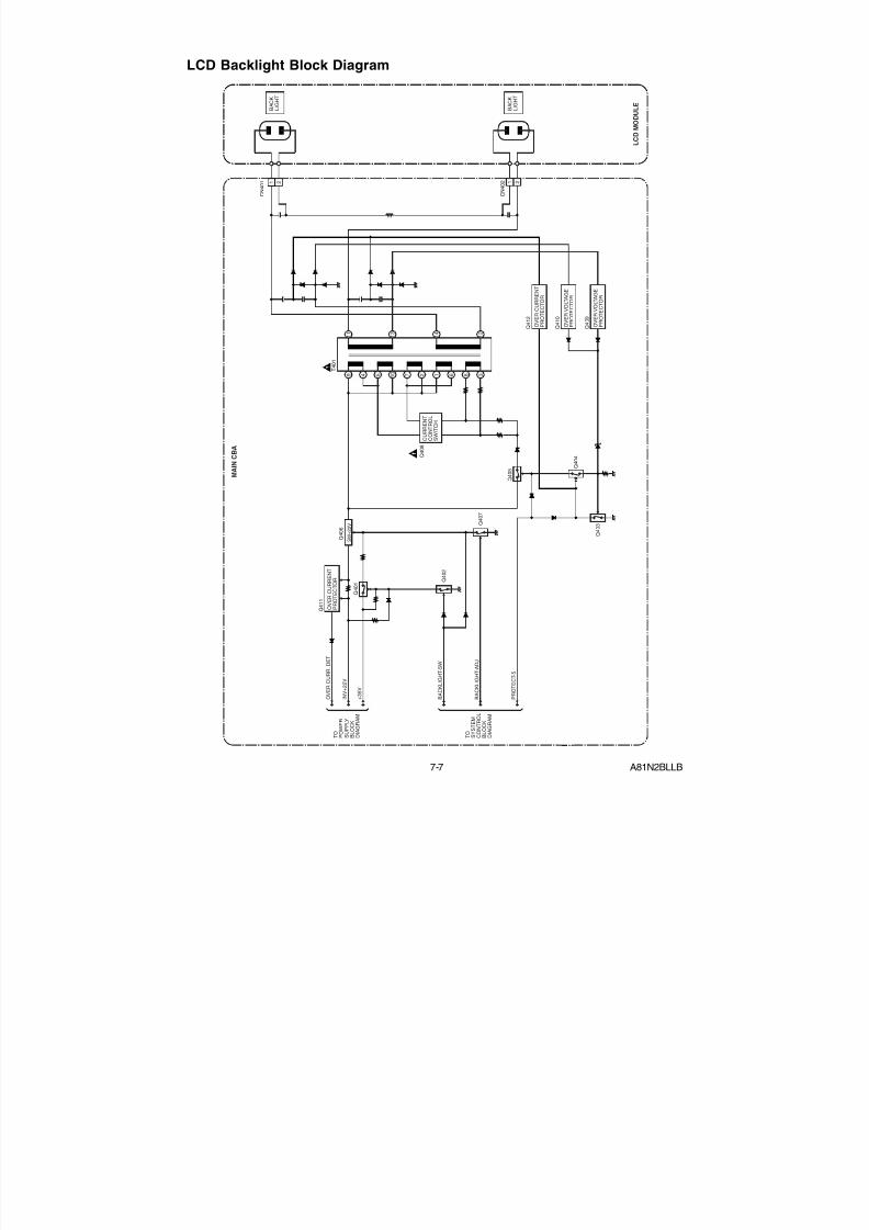
LCD Backlight Block Diagram
A81N2BLLB
C U R R E N T
C O N T R O L
S W I T C H
Q 4 0 8
Q 4 1 0
Q 4 0 9
Q 4 0 7
Q 4 0 2
Q 4 0 6
Q 4 0 5 Q
4 0 4
Q 4 0 3
Q 4 0 1
Q 4 1 1
C N 4 0 1
L C D M O D U L E
B A C K
L I G H T
B A C K
L I G H T
1 2
C N 4 0 2 1 2
I N V + 2 2 V
O V E R C U R R
. D E T
T O P O W E R
S U P P L Y
B L O C K
D I A G R A M
T O S Y S T E M
C O N T R O L
B L O C K
D I A G R A M
M A I N C B A
O V E R V O L T A G E
P R O T E C T O R
O V E R C U R R E N T
P R O T E C T O R
T 4 0 1
1 2 1 4 1 3 1 1
9 4 5 1 0 7 2 1 6 8 3
+ 3 5 V
B A C K L I G H T - A D J
S W + 2 2 V
B A C K L I G H T - S W
P R O T E C T - 5
O V E R V O L T A G E
P R O T E C T O R
Q 4 1 2
O V E R C U R R E N T
P R O T E C T O R
7/21/2019 Sylvania Lc195sl8 Lcd Tv Sm
http://slidepdf.com/reader/full/sylvania-lc195sl8-lcd-tv-sm 28/608-1 LC6N_SC
SCHEMATIC DIAGRAMS / CBA’S AND TEST POINTS
Standard Notes
WARNINGMany electrical and mechanical parts in this chassishave special characteristics. These characteristicsoften pass unnoticed and the protection afforded bythem cannot necessarily be obtained by usingreplacement components rated for higher voltage,wattage, etc. Replacement parts that have thesespecial safety characteristics are identified in thismanual and its supplements; electrical componentshaving such features are identified by the mark “# ” inthe schematic diagram and the parts list. Beforereplacing any of these components, read the parts listin this manual carefully. The use of substitutereplacement parts that do not have the same safetycharacteristics as specified in the parts list may createshock, fire, or other hazards.
Notes:1. Do not use the part number shown on these
drawings for ordering. The correct part number isshown in the parts list, and may be slightlydifferent or amended since these drawings wereprepared.
2. All resistance values are indicated in ohms(K = 103, M = 106).
3. Resistor wattages are 1/4W or 1/6W unlessotherwise specified.
4. All capacitance values are indicated inµF
(P = 10-6
µF).5. All voltages are DC voltages unless otherwisespecified.
7/21/2019 Sylvania Lc195sl8 Lcd Tv Sm
http://slidepdf.com/reader/full/sylvania-lc195sl8-lcd-tv-sm 29/608-2 LC6N_SC
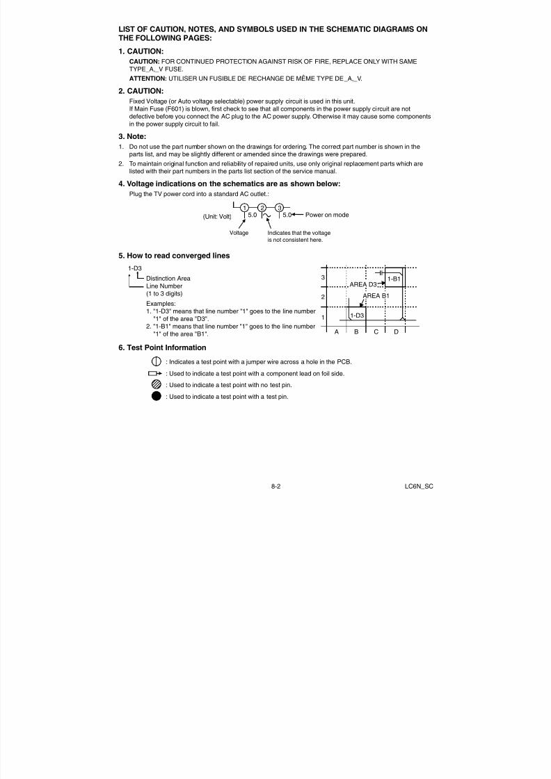
LIST OF CAUTION, NOTES, AND SYMBOLS USED IN THE SCHEMATIC DIAGRAMS ONTHE FOLLOWING PAGES:
1. CAUTION:CAUTION: FOR CONTINUED PROTECTION AGAINST RISK OF FIRE, REPLACE ONLY WITH SAMETYPE_A,_V FUSE.ATTENTION: UTILISER UN FUSIBLE DE RECHANGE DE MÊME TYPE DE_A,_V.
2. CAUTION:Fixed Voltage (or Auto voltage selectable) power supply circuit is used in this unit.If Main Fuse (F601) is blown, first check to see that all components in the power supply circuit are notdefective before you connect the AC plug to the AC power supply. Otherwise it may cause some componentsin the power supply circuit to fail.
3. Note:1. Do not use the part number shown on the drawings for ordering. The correct part number is shown in the
parts list, and may be slightly different or amended since the drawings were prepared.2. To maintain original function and reliability of repaired units, use only original replacement parts which are
listed with their part numbers in the parts list section of the service manual.
4. Voltage indications on the schematics are as shown below:
Plug the TV power cord into a standard AC outlet.:
5. How to read converged lines
6. Test Point Information
2 315.0 5.0
Voltage Indicates that the voltageis not consistent here.
Power on mode(Unit: Volt)
3
2
1
A B C D
1-B1
1-D3
AREA D3AREA B1
1-D3 Distinction Area
Line Number(1 to 3 digits)Examples:1. "1-D3" means that line number "1" goes to the line number "1" of the area "D3".2. "1-B1" means that line number "1" goes to the line number "1" of the area "B1".
: Indicates a test point with a jumper wire across a hole in the PCB.
: Used to indicate a test point with a component lead on foil side.
: Used to indicate a test point with no test pin.: Used to indicate a test point with a test pin.
7/21/2019 Sylvania Lc195sl8 Lcd Tv Sm
http://slidepdf.com/reader/full/sylvania-lc195sl8-lcd-tv-sm 30/60
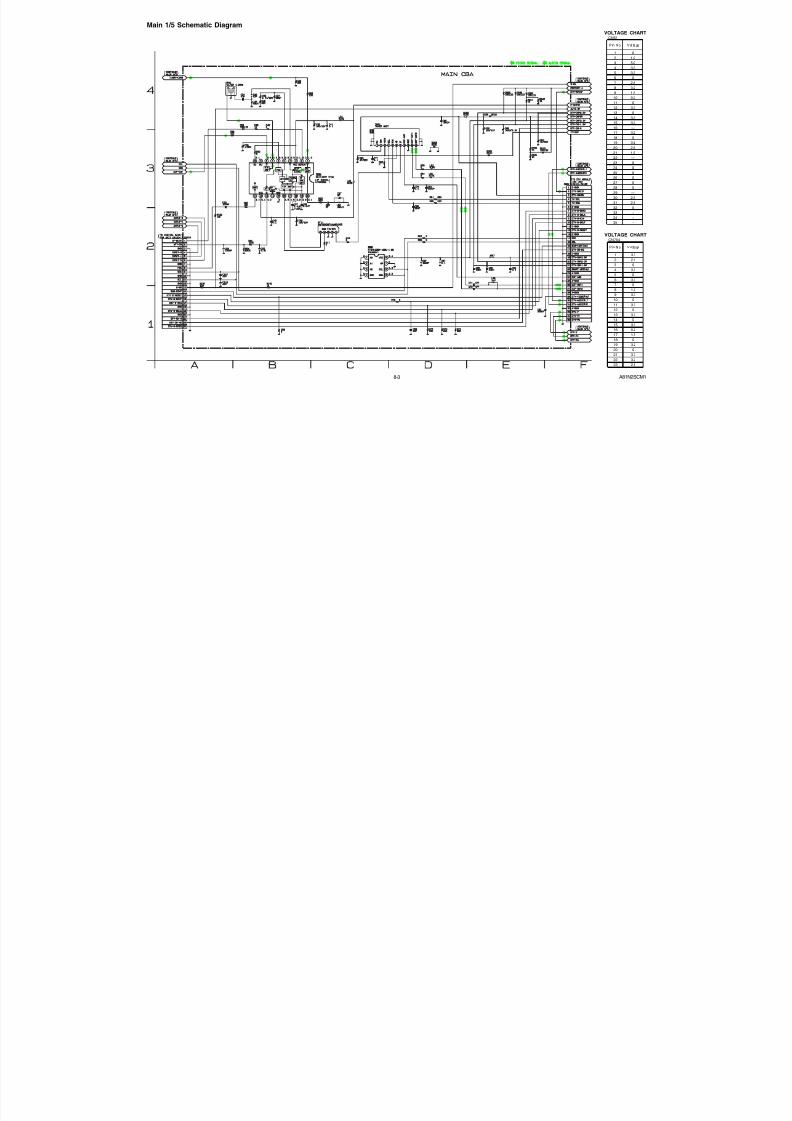
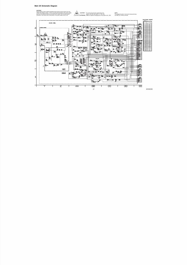
8-3 A81N2SCM
Main 1/5 Schematic Diagram
CN61
1 02 1.03 5.04 3.35 3.36 07 2.88 3.29 1.5
10 0.211 012 3.313 014 3.315 3.316 ---17 3.2
18 019 3.420 2.621 1.922 ---23 024 025 026 027 028 029 ---30 2.531 2.532 033 ~34 ~35 ~
VOLTAGE CHAR
P in N o. Vol ta ge
CN704
1 3.32 2.13 04 3.3
5 06 3.37 08 1.09 3.3
10 011 3.312 013 3.314 015 3.316 0.217 1.518 019 3.220 021 3.322 3.223 2.8
VOLTAGE CHAR
P in N o. Vol ta ge
7/21/2019 Sylvania Lc195sl8 Lcd Tv Sm
http://slidepdf.com/reader/full/sylvania-lc195sl8-lcd-tv-sm 31/60
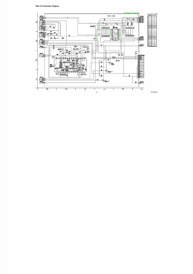
8-4 A81N2SCM
Main 2/5 Schematic Diagram
CN702
1 3.12 2.43 1.84 3.35 06 ---7 ---8 ---9 ---
10 ---11 012 ---
13 ---14 ---15 ---16 017 ---18 019 3.320 021 ---22 3.323 ---
VOLTAGE CHAR
P in N o. Vol ta ge
7/21/2019 Sylvania Lc195sl8 Lcd Tv Sm
http://slidepdf.com/reader/full/sylvania-lc195sl8-lcd-tv-sm 32/60
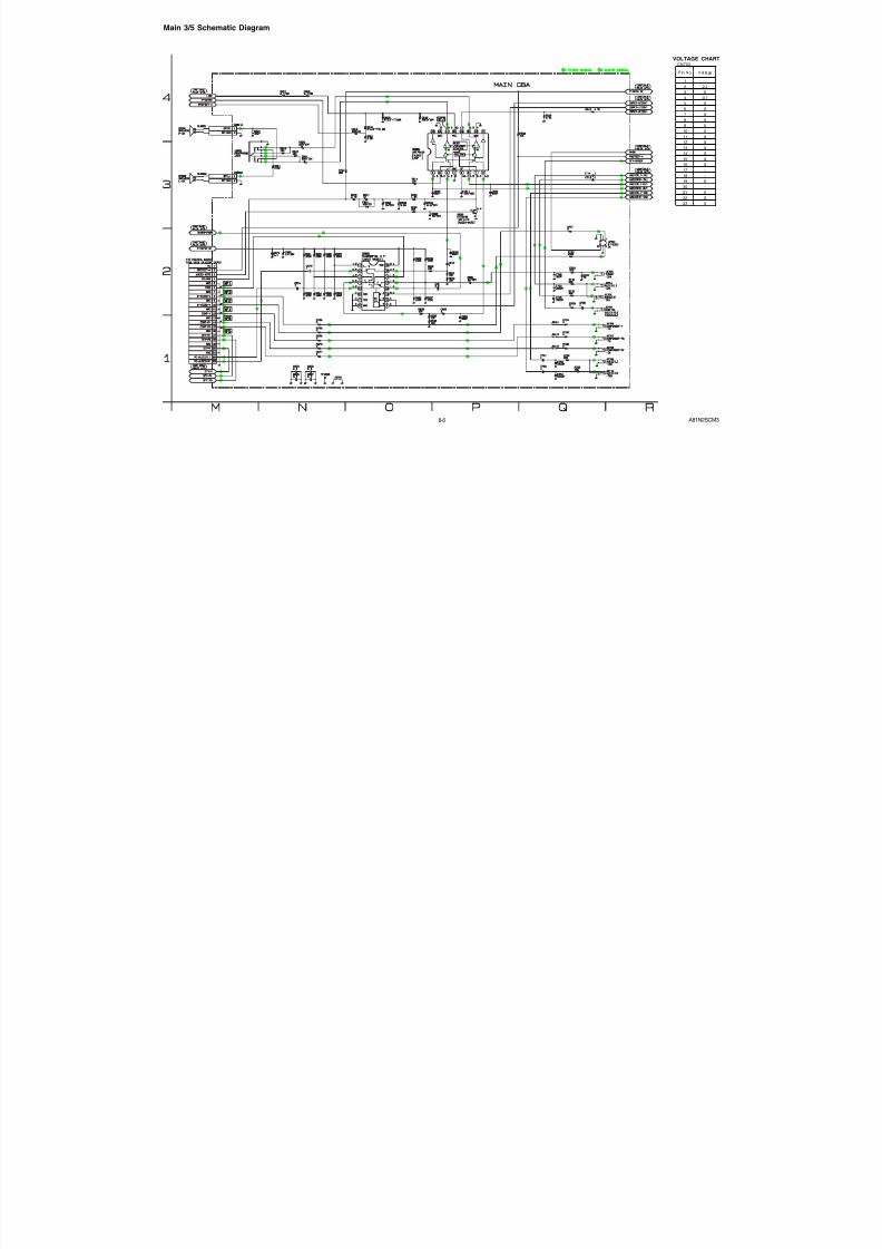
8-5 A81N2SCM
Main 3/5 Schematic Diagram
CN703
1 ---2 2.23 04 0.75 06 07 08 09 0
10 011 012 013 0
14 015 016 017 ~18 ~19 020 ~21 022 023 0
VOLTAGE CHAR
P in N o. Vol ta ge
7/21/2019 Sylvania Lc195sl8 Lcd Tv Sm
http://slidepdf.com/reader/full/sylvania-lc195sl8-lcd-tv-sm 33/60
8-6 A81N2SCM
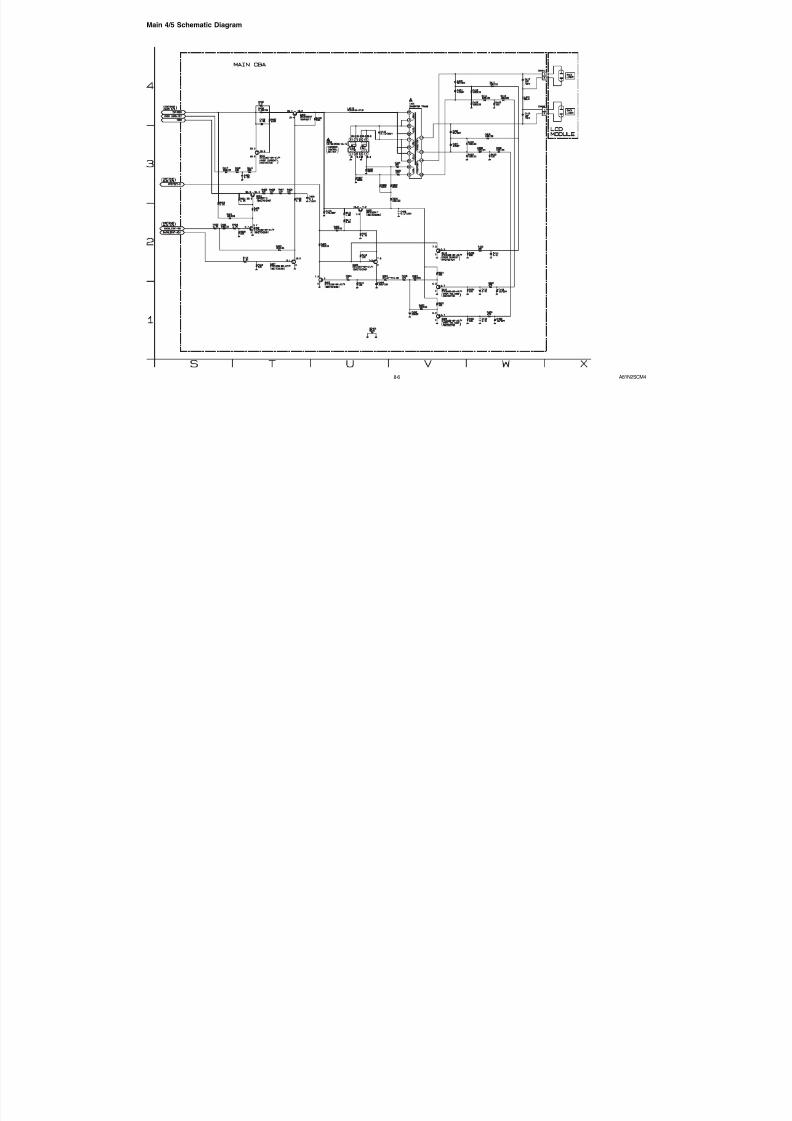
Main 4/5 Schematic Diagram
7/21/2019 Sylvania Lc195sl8 Lcd Tv Sm
http://slidepdf.com/reader/full/sylvania-lc195sl8-lcd-tv-sm 34/60
8-7
For continued protection against risk of fire,replace only with same type 4 A, 125V fuse.
CAUTION ! :
ATTENTION : Utiliser un fusible de rechange de m ê me type de 4A, 125V.4A/125V
CAUTION !Fixed voltage (or Auto voltage selectable) power supply circuit is used in this unit.If Main Fuse (F601) is blown , check to see that all components in the power supplycircuit are not defective before you connect the AC plug to the AC power supply.Otherwise it may cause some components in the power supply circuit to fail.
NOTE:
The voltage for parts in hot circuit is measured usinghot GND as a common terminal.
A81N2SCM
Main 5/5 Schematic Diagram
CN701
1 3.42 3.43 0.44 3.35 2.16 5.17 0
8 3.49 3.4
10 011 012 1.513 1.514 3.415 016 13.117 3.318 -7.019 3.320 24.421 022 023 3.3
VOLTAGE CHAR
P in N o. Vol ta ge
7/21/2019 Sylvania Lc195sl8 Lcd Tv Sm
http://slidepdf.com/reader/full/sylvania-lc195sl8-lcd-tv-sm 35/60
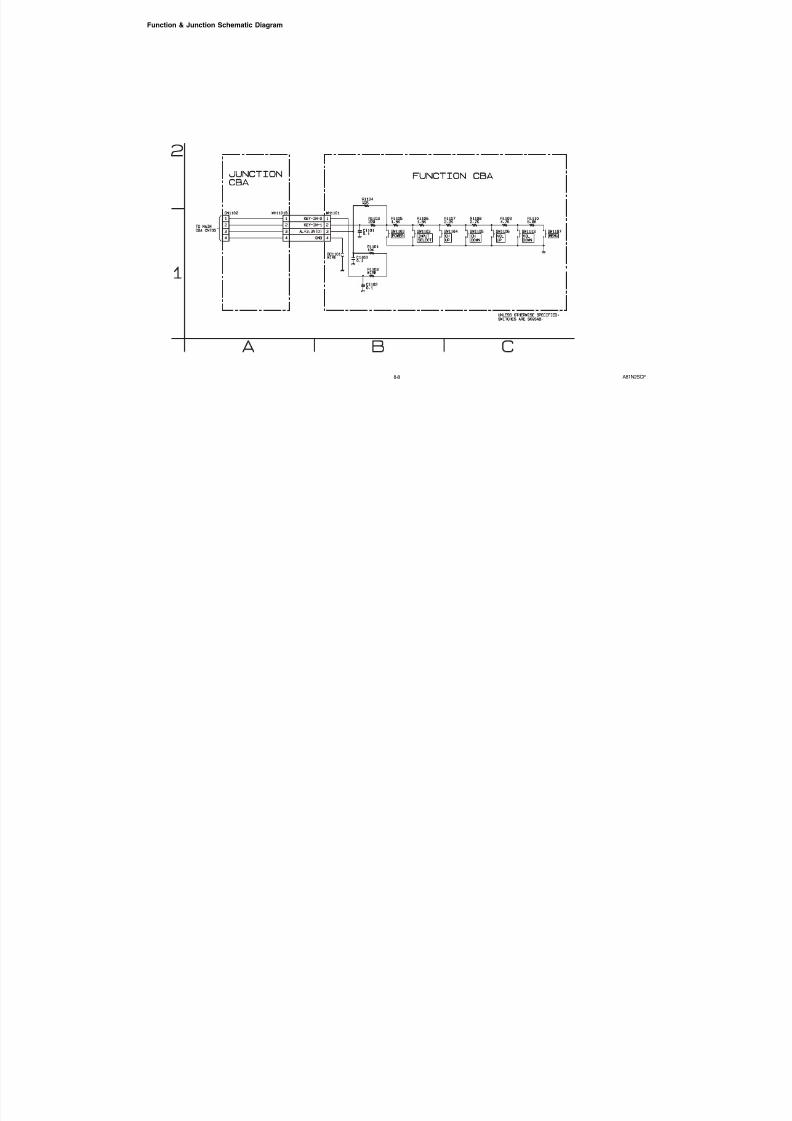
8-8 A81N2SC
Function & Junction Schematic Diagram
7/21/2019 Sylvania Lc195sl8 Lcd Tv Sm
http://slidepdf.com/reader/full/sylvania-lc195sl8-lcd-tv-sm 36/60
8-9 A81N2SC
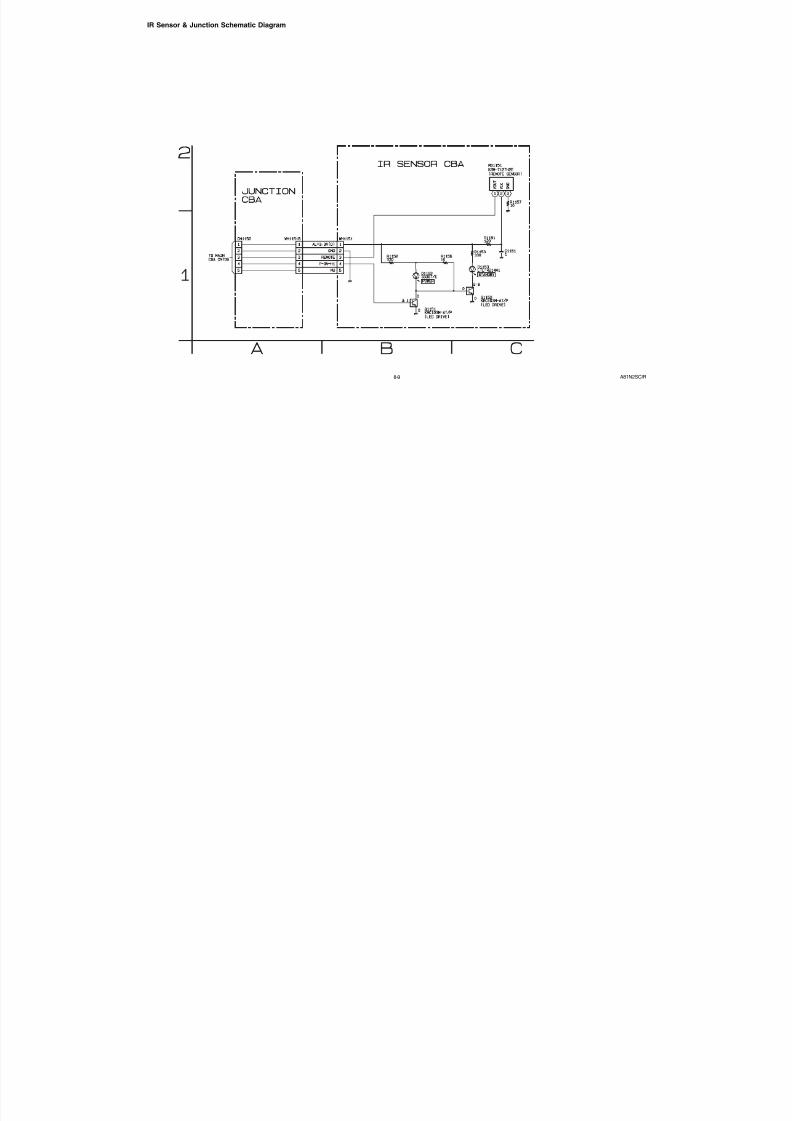
IR Sensor & Junction Schematic Diagram
7/21/2019 Sylvania Lc195sl8 Lcd Tv Sm
http://slidepdf.com/reader/full/sylvania-lc195sl8-lcd-tv-sm 37/60
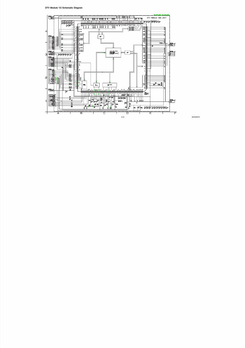
8-10 A81N2SCD
DTV Module 1/2 Schematic Diagram
7/21/2019 Sylvania Lc195sl8 Lcd Tv Sm
http://slidepdf.com/reader/full/sylvania-lc195sl8-lcd-tv-sm 38/60
8-11 A81N2SCD
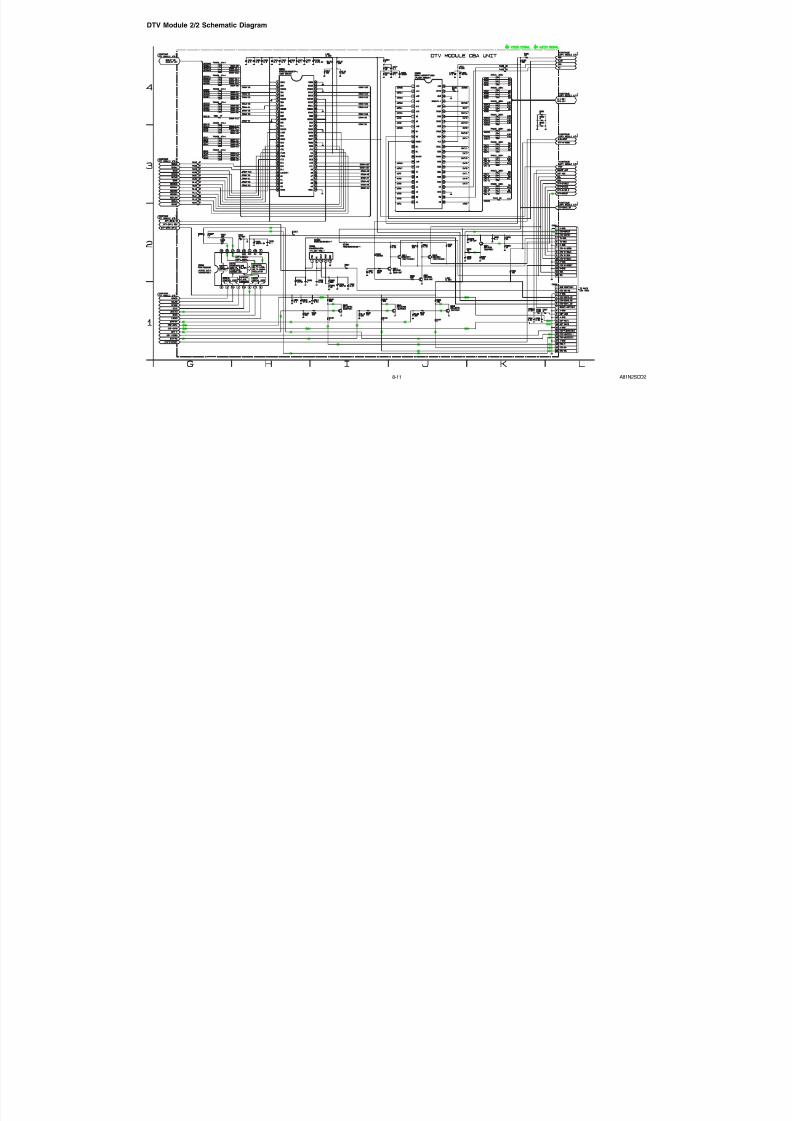
DTV Module 2/2 Schematic Diagram
7/21/2019 Sylvania Lc195sl8 Lcd Tv Sm
http://slidepdf.com/reader/full/sylvania-lc195sl8-lcd-tv-sm 39/60
8-12 A81N2SCDM
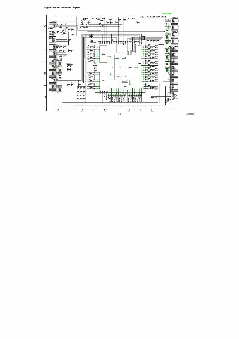
Digital Main 1/6 Schematic Diagram
7/21/2019 Sylvania Lc195sl8 Lcd Tv Sm
http://slidepdf.com/reader/full/sylvania-lc195sl8-lcd-tv-sm 40/60
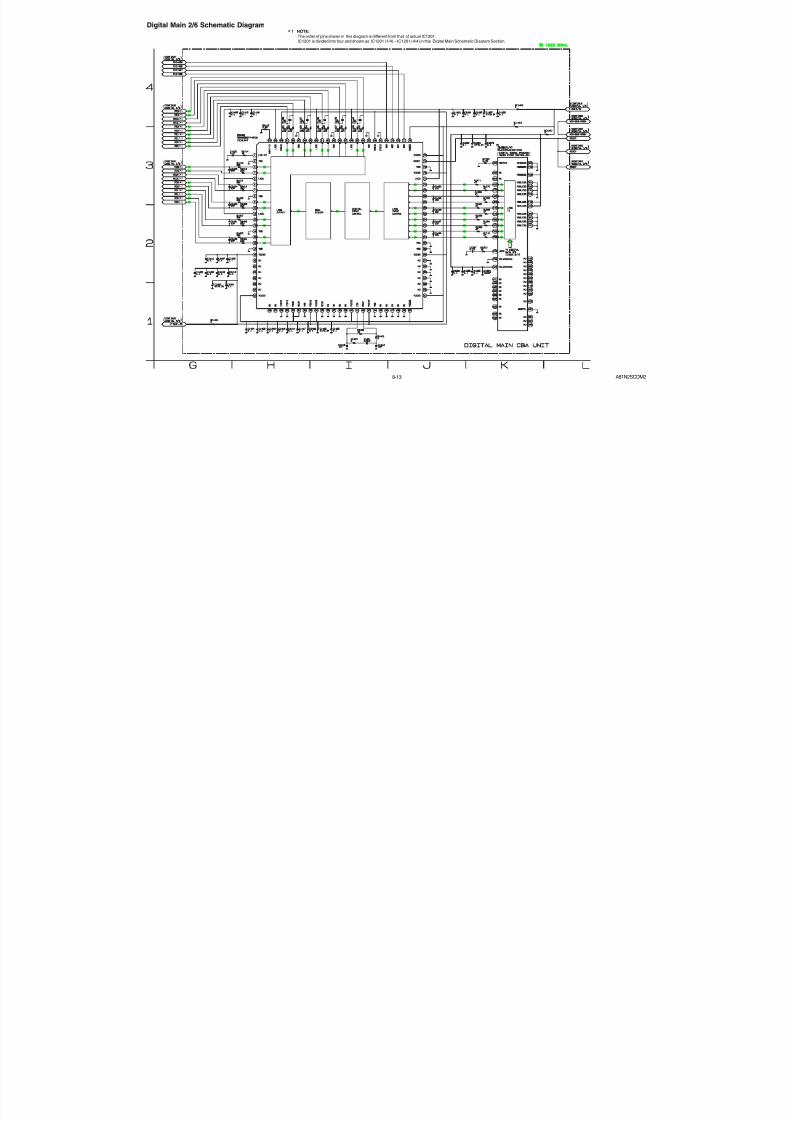
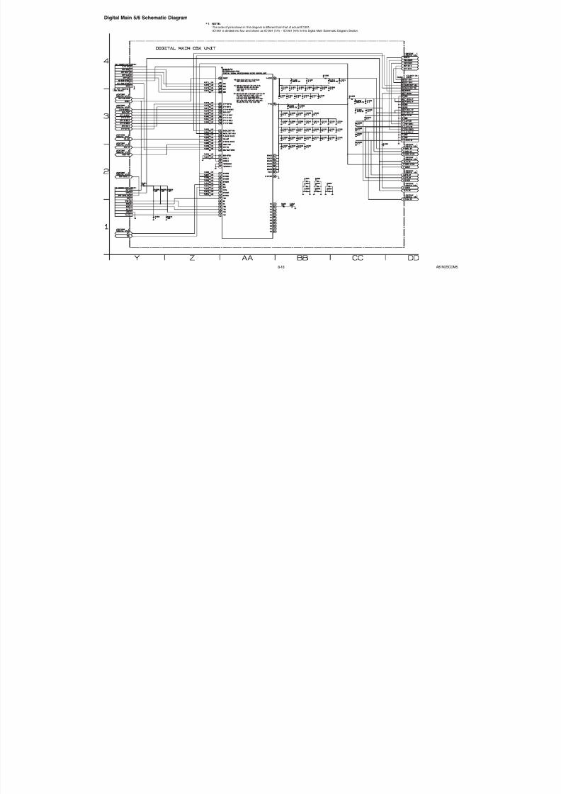
8-13 A81N2SCDM
Digital Main 2/6 Schematic DiagramThe order of pins shown in this diagram is different from that of actual IC1201.IC1201 is divided into four and shown as IC1201 (1/4) ~ IC1201 (4/4) in this Digital Main Schematic Diagram Section.
1 NOTE:
7/21/2019 Sylvania Lc195sl8 Lcd Tv Sm
http://slidepdf.com/reader/full/sylvania-lc195sl8-lcd-tv-sm 41/60
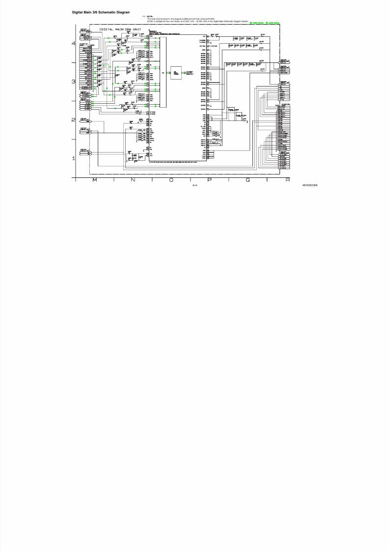
8-14 A81N2SCDM
Digital Main 3/6 Schematic Diagram
The order of pins shown in this diagram is different from that of actual IC1201.IC1201 is divided into four and shown as IC1201 (1/4) ~ IC1201 (4/4) in this Digital Main Schematic Diagram Section.
1 NOTE:

7/21/2019 Sylvania Lc195sl8 Lcd Tv Sm
http://slidepdf.com/reader/full/sylvania-lc195sl8-lcd-tv-sm 42/60
8-15 A81N2SCDM
Digital Main 4/6 Schematic Diagram
The order of pins shown in this diagram is different from that of actual IC1201.IC1201 is divided into four and shown as IC1201 (1/4) ~ IC1201 (4/4) in this Digital Main Schematic Diagram Section.
1 NOTE:
7/21/2019 Sylvania Lc195sl8 Lcd Tv Sm
http://slidepdf.com/reader/full/sylvania-lc195sl8-lcd-tv-sm 43/60
8-16 A81N2SCDM
Digital Main 5/6 Schematic Diagram
The order of pins shown in this diagram is different from that of actual IC1201.IC1201 is divided into four and shown as IC1201 (1/4) ~ IC1201 (4/4) in this Digital Main Schematic Diagram Section.
1 NOTE:
7/21/2019 Sylvania Lc195sl8 Lcd Tv Sm
http://slidepdf.com/reader/full/sylvania-lc195sl8-lcd-tv-sm 44/60
8-17 A81N2SCDM
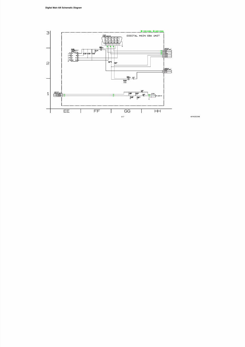
Digital Main 6/6 Schematic Diagram
7/21/2019 Sylvania Lc195sl8 Lcd Tv Sm
http://slidepdf.com/reader/full/sylvania-lc195sl8-lcd-tv-sm 45/60
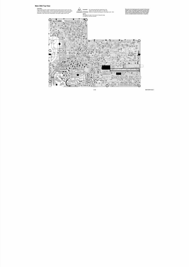
8-18 BA81N0F01022-
Main CBA Top View
Because a hot chassis ground is present in the powersupply circuit, an isolation transformer must be used.Also, in order to have the ability to increase the inputslowly,when troubleshooting this type power supplycircuit, a variable isolation transformer is required.
For continued protection against risk of fire,replace only with same type 4 A, 125V fuse.
CAUTION ! :
ATTENTION : Utiliser un fusible de rechange de m ême type de 4A, 125V.4A/125V
CAUTION !Fixed voltage (or Auto voltage selectable) power supply circuit is used in this unit.If Main Fuse (F601) is blown , check to see that all components in the power supplycircuit are not defective before you connect the AC plug to the AC power supply.Otherwise it may cause some components in the power supply circuit to fail.
NOTE:The voltage for parts in hot circuit is measured usinghot GND as a common terminal.
7/21/2019 Sylvania Lc195sl8 Lcd Tv Sm
http://slidepdf.com/reader/full/sylvania-lc195sl8-lcd-tv-sm 46/60
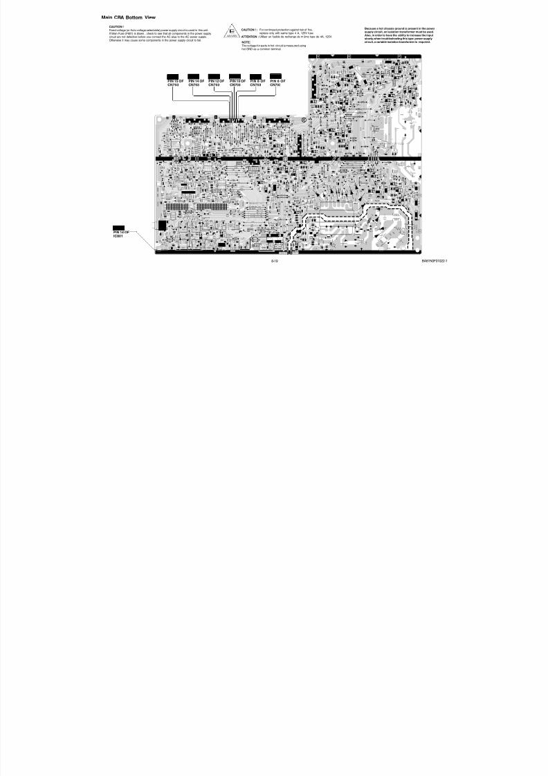
8-19
PIN 10 OFCN703
WF2PIN 12 OFCN703
WF4PIN 6 OFCN703
WF1PIN 14 OFCN703
WF6PIN 8 OFCN703
WF3PIN 15 OFCN703
WF5
PIN 14 OFIC801
WF7
Main CBA Bottom View
BA81N0F01022
Because a hot chassis ground is present in the powersupply circuit, an isolation transformer must be used.Also, in order to have the ability to increase the inputslowly,when troubleshooting this type power supplycircuit, a variable isolation transformer is required.
For continued protection against risk of fire,replace only with same type 4 A, 125V fuse.
CAUTION ! :
ATTENTION : Utiliser un fusible de rechange de m ême type de 4A, 125V.4A/125V
CAUTION !Fixed voltage (or Auto voltage selectable) power supply circuit is used in this unit.If Main Fuse (F601) is blown , check to see that all components in the power supplycircuit are not defective before you connect the AC plug to the AC power supply.Otherwise it may cause some components in the power supply circuit to fail.
NOTE:The voltage for parts in hot circuit is measured usinghot GND as a common terminal.
7/21/2019 Sylvania Lc195sl8 Lcd Tv Sm
http://slidepdf.com/reader/full/sylvania-lc195sl8-lcd-tv-sm 47/60
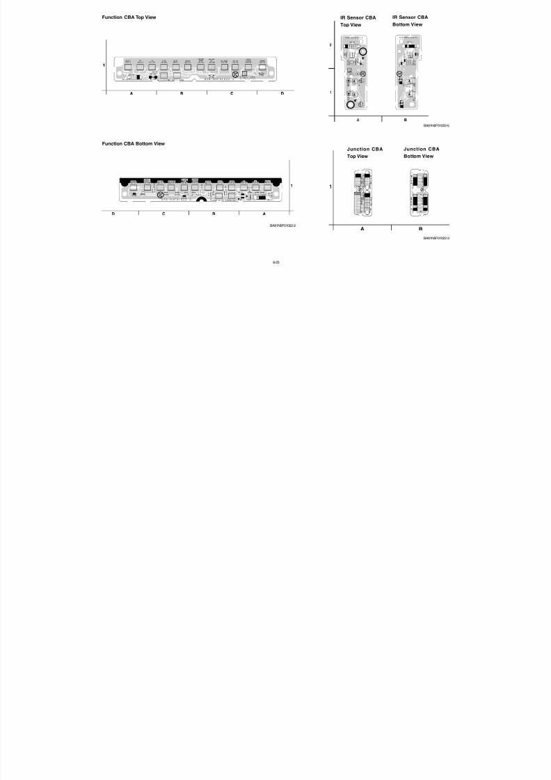
8-20
Function CBA Top View
Function CBA Bottom View
BA81N0F01022-2
IR Sensor CBATop View
IR Sensor CBABottom View
BA81N0F01022-
BA81N0F01022-
Junction CBATop View
Junction CBABottom View
7/21/2019 Sylvania Lc195sl8 Lcd Tv Sm
http://slidepdf.com/reader/full/sylvania-lc195sl8-lcd-tv-sm 48/60
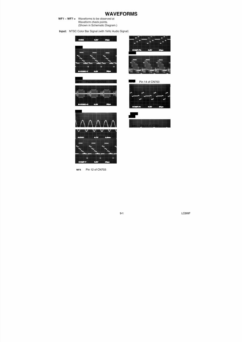
WAVEFORMS
LC6WF9-1
Input: NTSC Color Bar Signal (with 1kHz Audio Signal)
WF1 ~ WF7 = Waveforms to be observed atWaveform check points.(Shown in Schematic Diagram.)
C VBS 0.2V 20 s
WF1 Pin 6 of CN703
S V IDE O Y 0.2V
WF2 Pin 10 of CN703
20 s
S V IDE O C 0.2V
WF3 Pin 8 of CN703
20 s AUD IO 0.1V 0.5m s
WF7 Pin 14 of IC801
CO M P Pr 0.2V 20 s
Pin 14 of CN703WF6
CO M P Pb 0.2V 20 s
Pin 15 of CN703WF5
C O M P Y 0.2V 20 s
Pin 12 of CN703WF4
7/21/2019 Sylvania Lc195sl8 Lcd Tv Sm
http://slidepdf.com/reader/full/sylvania-lc195sl8-lcd-tv-sm 49/60

7/21/2019 Sylvania Lc195sl8 Lcd Tv Sm
http://slidepdf.com/reader/full/sylvania-lc195sl8-lcd-tv-sm 50/60
11-1
EXPLODED VIEWS
Cabinet
A13
A1
A23
L1L1
L1
L3
L3
L3
B5
L3
L3
L3
L4
L2
B3
B3
L1
L1
L1
L1
A7A3
L1SP801
SP802
See Electrical Parts Listfor parts with this mark. Main CBA
AC601
Function CBA
IR Sensor CBA
B11
B11
B11
B10
B2 L1
L1
L3
L1
L4
L4
L4
B6
B9
DTV CBA
A
LCD1A11
L1
L3
Digital Main CBA Unit
Junction CBA
CLN802
CL1901CL1902
L3
L19
CLN801
7/21/2019 Sylvania Lc195sl8 Lcd Tv Sm
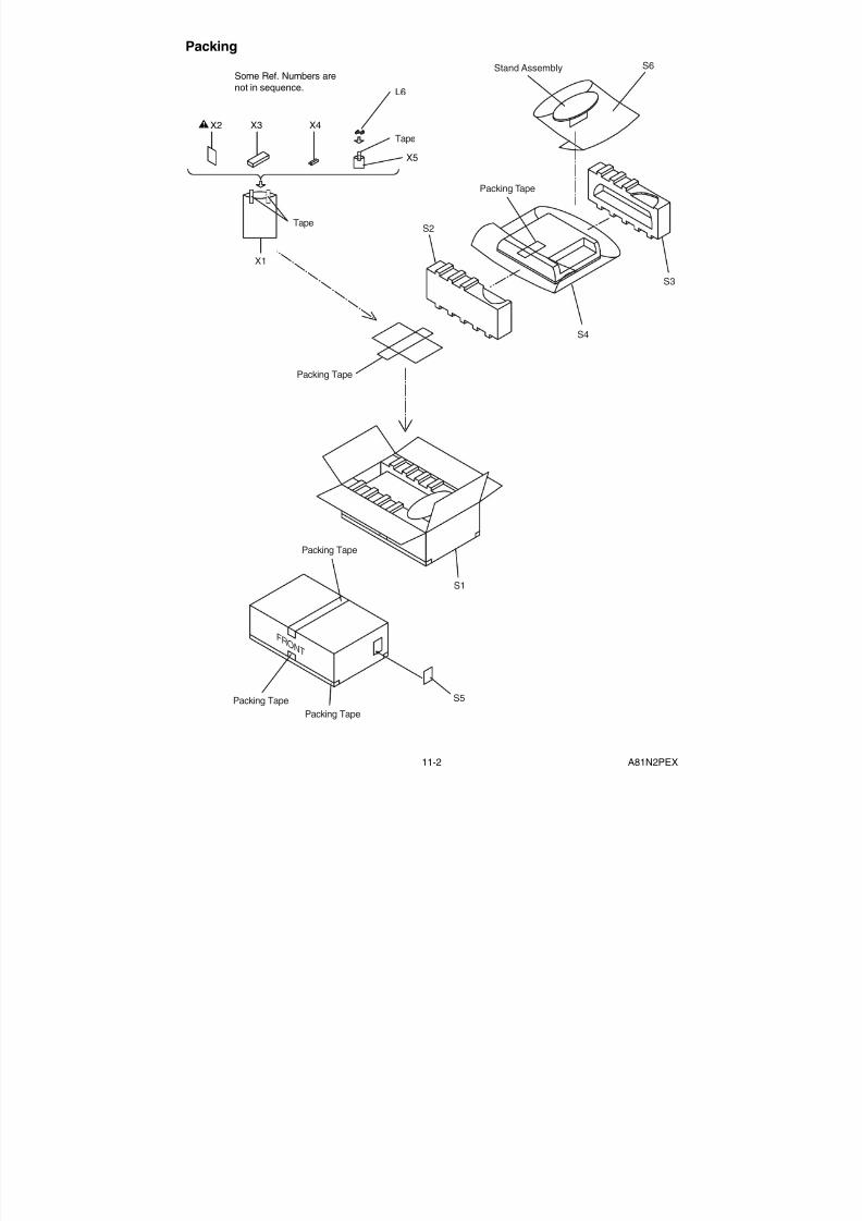
http://slidepdf.com/reader/full/sylvania-lc195sl8-lcd-tv-sm 51/6011-2 A81N2PEX
Packing
S1
FRONT
S3
S6
S4
Tape
Tape
Packing TapePacking Tape
Packing Tape
S2
X1
Some Ref. Numbers arenot in sequence.
X4
X5
L6
X3X2
Packing Tape
Stand Assembly
Packing Tape
S5

7/21/2019 Sylvania Lc195sl8 Lcd Tv Sm
http://slidepdf.com/reader/full/sylvania-lc195sl8-lcd-tv-sm 52/6020071001 12-1 A81N2CA
MECHANICAL PARTS LISTPRODUCT SAFETY NOTE: Products marked with a# have special characteristics important to safety.Before replacing any of these components, readcarefully the product safety notice in this servicemanual. Don't degrade the safety of the productthrough improper servicing.NOTE: Parts that are not assigned part numbers(---------) are not available.
Ref. No. Description Part No.
A1 FRONT CABINET A81N2UH 1EM122053A3 CONTROL PLATE A81H0UH 1EM322723A4 REAR CABIET A81N2UH 1EM021845A6# RATING LABEL A81N2UH ----------A7 FUNCTION KNOB A81H0UH 1EM121947A9 STAND COVER A81N2UH 1EM221703A10 REAR COVER A7260JH 1EM322484A11 LED LENS A81N0UH 1EM322707
A12 STAND RUBBER FOOT L5001CB 1EM423855A13 SENSOR LENS A81N0UH 1EM322708A23 ENERGY STAR LABEL A81H0UH ----------B2 TILT STAND HOLDER A81N0UH 1EM322710B3 STAND HOLDER A81N0UH 1EM322709B5 JACK HOLDER(D) A81N0UH 1EM322706B6 JACK HOLDER(A) A81N0UH 1EM322705B7 ARM ASSEMBLY A72N0JH 1EM221634B9 MODULE PCB HOLDER P7150UT 1EM322373ACL1901 WIRE ASSEMBLY FFC FFC 40PIN WX1A81N0-01ACL1902 WIRE ASSEMBLY FFC FFC 40PIN WX1A81N0-01ACLN801 WIRE ASSEMBLY SPEAKER 2PIN AWG24 WX1A81N0-05ACLN802 WIRE ASSEMBLY SPEAKER 2PIN AWG24 WX1A81N0-05AL1 SCREW P-TIGHT M3X10 BIND HEAD+ GBJP3100
L2 SCREW P-TIGHT 3X10 BIND HEAD+ GBHP3100L3 SCREW S-TIGHT M3X6 BIND HEAD+ GBJS3060L6 DOUBLE SEMS SCREW M4X14 + BLK FPH34140L19 HEX SCREW #4-40 7MM 1EM422042LCD1 LCD MODULE 19INCH WIDE SVA 19INCH
WXGAUG190XB
SP801 SPEAKER MAGNETIC S0306N01 DSD0806XQ001SP802 SPEAKER MAGNETIC S0306N01 DSD0806XQ001
PACKINGS1 CARTON A81N2UH 1EM322977S2 STYROFOAM BOTTOM A81N0UH 1EM021790S3 STYROFOAM TOP A81N0UH 1EM021789S4 SET BAG A81N0UH 1EM322872AS5 SERIAL NO. LABEL L9750UA ----------
S6 STAND BAG A81N0UH 1EM424597ACCESSORIES
X1 BAG POLYETHYLENE 235X365XT0.03 0EM408420AX2# OWNERS MANUAL A81N2UH 1EMN22419X3 REMOTE CONTROL NF604UD NF604UD NF604UDX4 DRY BATTERY(SUNRISE) R6SSE/2S XB0M451MS002X5 SCREW BAG A81N0UH 1EM424596A
7/21/2019 Sylvania Lc195sl8 Lcd Tv Sm
http://slidepdf.com/reader/full/sylvania-lc195sl8-lcd-tv-sm 53/6020071001 13-1 A81N2EL
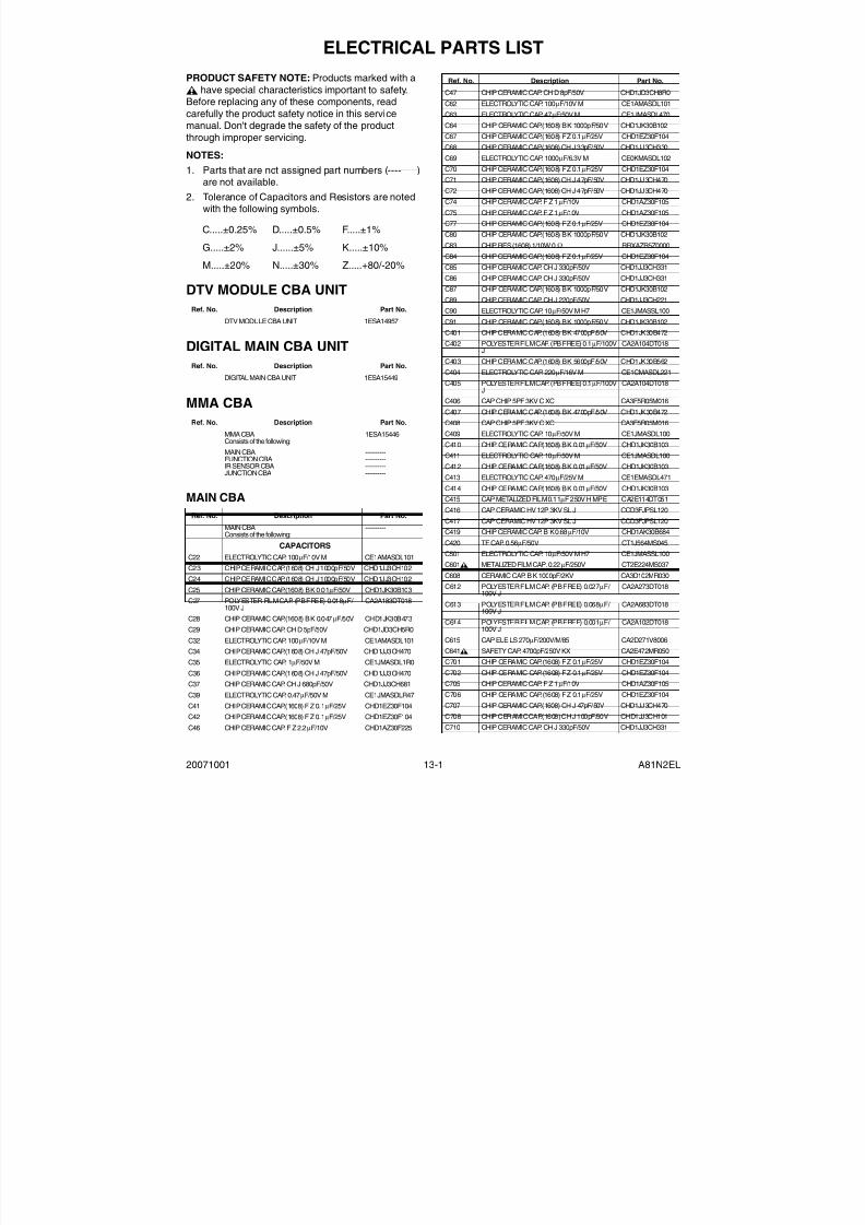
ELECTRICAL PARTS LISTPRODUCT SAFETY NOTE: Products marked with a# have special characteristics important to safety.Before replacing any of these components, readcarefully the product safety notice in this servicemanual. Don't degrade the safety of the productthrough improper servicing.
NOTES:1. Parts that are not assigned part numbers (---------)
are not available.2. Tolerance of Capacitors and Resistors are noted
with the following symbols.
DTV MODULE CBA UNIT
DIGITAL MAIN CBA UNIT
MMA CBA
MAIN CBA
C.....±0.25% D.....±0.5% F.....±1%
G.....±2% J......±5% K.....±10%
M.....±20% N.....±30% Z.....+80/-20%
Ref. No. Description Part No.
DTV MODULE CBA UNIT 1ESA14957
Ref. No. Description Part No.
DIGITAL MAIN CBA UNIT 1ESA15449
Ref. No. Description Part No.
MMA CBAConsists of the following:
1ESA15446
MAIN CBAFUNCTION CBAIR SENSOR CBAJUNCTION CBA
----------------------------------------
Ref. No. Description Part No.
MAIN CBAConsists of the following:
----------
CAPACITORSC22 ELECTROLYTIC CAP. 100 µF/10V M CE1AMASDL101C23 CHIP CERAMIC CAP.(1608) CH J 1000pF/50V CHD1JJ3CH102
C24 CHIP CERAMIC CAP.(1608) CH J 1000pF/50V CHD1JJ3CH102
C25 CHIP CERAMIC CAP.(1608) B K 0.01 µF/50V CHD1JK30B103C27 POLYESTER FILM CAP. (PB FREE) 0.018 µF/
100V JCA2A183DT018
C28 CHIP CERAMIC CAP.(1608) B K 0.047 µF/50V CHD1JK30B473
C29 CHIP CERAMIC CAP. CH D 5pF/50V CHD1JD3CH5R0
C32 ELECTROLYTIC CAP. 100 µF/10V M CE1AMASDL101C34 CHIP CERAMIC CAP.(1608) CH J 47pF/50V CHD1JJ3CH470
C35 ELECTROLYTIC CAP. 1 µF/50V M CE1JMASDL1R0
C36 CHIP CERAMIC CAP.(1608) CH J 47pF/50V CHD1JJ3CH470C37 CHIP CERAMIC CAP. CH J 680pF/50V CHD1JJ3CH681
C39 ELECTROLYTIC CAP. 0.47 µF/50V M CE1JMASDLR47
C41 CHIP CERAMIC CAP.(1608) F Z 0.1 µF/25V CHD1EZ30F104C42 CHIP CERAMIC CAP.(1608) F Z 0.1 µF/25V CHD1EZ30F104
C46 CHIP CERAMIC CAP. F Z 2.2 µF/10V CHD1AZ30F225
C47 CHIP CERAMIC CAP. CH D 8pF/50V CHD1JD3CH8R0
C62 ELECTROLYTIC CAP. 100 µF/10V M CE1AMASDL101
C63 ELECTROLYTIC CAP. 47 µF/50V M CE1JMASDL470
C64 CHIP CERAMIC CAP.(1608) B K 1000pF/50V CHD1JK30B102
C67 CHIP CERAMIC CAP.(1608) F Z 0.1 µF/25V CHD1EZ30F104
C68 CHIP CERAMIC CAP.(1608) CH J 33pF/50V CHD1JJ3CH330
C69 ELECTROLYTIC CAP. 1000 µF/6.3V M CE0KMASDL102
C70 CHIP CERAMIC CAP.(1608) F Z 0.1 µF/25V CHD1EZ30F104
C71 CHIP CERAMIC CAP.(1608) CH J 47pF/50V CHD1JJ3CH470
C72 CHIP CERAMIC CAP.(1608) CH J 47pF/50V CHD1JJ3CH470
C74 CHIP CERAMIC CAP. F Z 1 µF/10V CHD1AZ30F105
C75 CHIP CERAMIC CAP. F Z 1 µF/10V CHD1AZ30F105C77 CHIP CERAMIC CAP.(1608) F Z 0.1 µF/25V CHD1EZ30F104
C80 CHIP CERAMIC CAP.(1608) B K 1000pF/50V CHD1JK30B102
C83 CHIP RES.(1608) 1/10W 0 Ω RRXAZR5Z0000
C84 CHIP CERAMIC CAP.(1608) F Z 0.1 µF/25V CHD1EZ30F104
C85 CHIP CERAMIC CAP. CH J 330pF/50V CHD1JJ3CH331
C86 CHIP CERAMIC CAP. CH J 330pF/50V CHD1JJ3CH331
C87 CHIP CERAMIC CAP.(1608) B K 1000pF/50V CHD1JK30B102
C89 CHIP CERAMIC CAP. CH J 220pF/50V CHD1JJ3CH221C90 ELECTROLYTIC CAP. 10 µF/50V M H7 CE1JMASSL100
C91 CHIP CERAMIC CAP.(1608) B K 1000pF/50V CHD1JK30B102C401 CHIP CERAMIC CAP.(1608) B K 4700pF/50V CHD1JK30B472
C402 POLYESTER FILM CAP. (PB FREE) 0.1 µF/100VJ
CA2A104DT018
C403 CHIP CERAMIC CAP.(1608) B K 5600pF/50V CHD1JK30B562
C404 ELECTROLYTIC CAP. 220 µF/16V M CE1CMASDL221
C405 POLYESTER FILM CAP. (PB FREE) 0.1 µF/100VJ
CA2A104DT018
C406 CAP CHIP 5PF 3KV C XC CA3F5R05M016
C407 CHIP CERAMIC CAP.(1608) B K 4700pF/50V CHD1JK30B472
C408 CAP CHIP 5PF 3KV C XC CA3F5R05M016
C409 ELECTROLYTIC CAP. 10 µF/50V M CE1JMASDL100
C410 CHIP CERAMIC CAP.(1608) B K 0.01 µF/50V CHD1JK30B103
C411 ELECTROLYTIC CAP. 10 µF/50V M CE1JMASDL100C412 CHIP CERAMIC CAP.(1608) B K 0.01 µF/50V CHD1JK30B103
C413 ELECTROLYTIC CAP. 470 µF/25V M CE1EMASDL471
C414 CHIP CERAMIC CAP.(1608) B K 0.01 µF/50V CHD1JK30B103C415 CAP METALIZED FILM 0.11 µF 250V H MPE CA2E114DT051
C416 CAP CERAMIC HV 12P 3KV SL J CCD3FJPSL120
C417 CAP CERAMIC HV 12P 3KV SL J CCD3FJPSL120C419 CHIP CERAMIC CAP. B K 0.68 µF/10V CHD1AK30B684
C420 TF CAP. 0.56 µF/50V CT1J564MS045
C501 ELECTROLYTIC CAP. 10 µF/50V M H7 CE1JMASSL100C601 # METALIZED FILM CAP. 0.22 µF/250V CT2E224MS037
C608 CERAMIC CAP. B K 1000pF/2KV CA3D102MR030
C612 POLYESTER FILM CAP. (PB FREE) 0.027 µF/ 100V J
CA2A273DT018
C613 POLYESTER FILM CAP. (PB FREE) 0.068 µF/ 100V J CA2A683DT018
C614 POLYESTER FILM CAP. (PB FREE) 0.001 µF/ 100V J
CA2A102DT018
C615 CAP ELE LS 270 µF/200V/M/85 CA2D271V8006
C641 # SAFETY CAP. 4700pF/250V KX CA2E472MR050
C701 CHIP CERAMIC CAP.(1608) F Z 0.1 µF/25V CHD1EZ30F104
C702 CHIP CERAMIC CAP.(1608) F Z 0.1 µF/25V CHD1EZ30F104
C705 CHIP CERAMIC CAP. F Z 1 µF/10V CHD1AZ30F105
C706 CHIP CERAMIC CAP.(1608) F Z 0.1 µF/25V CHD1EZ30F104
C707 CHIP CERAMIC CAP.(1608) CH J 47pF/50V CHD1JJ3CH470
C708 CHIP CERAMIC CAP.(1608) CH J 100pF/50V CHD1JJ3CH101
C710 CHIP CERAMIC CAP. CH J 330pF/50V CHD1JJ3CH331
Ref. No. Description Part No.
7/21/2019 Sylvania Lc195sl8 Lcd Tv Sm
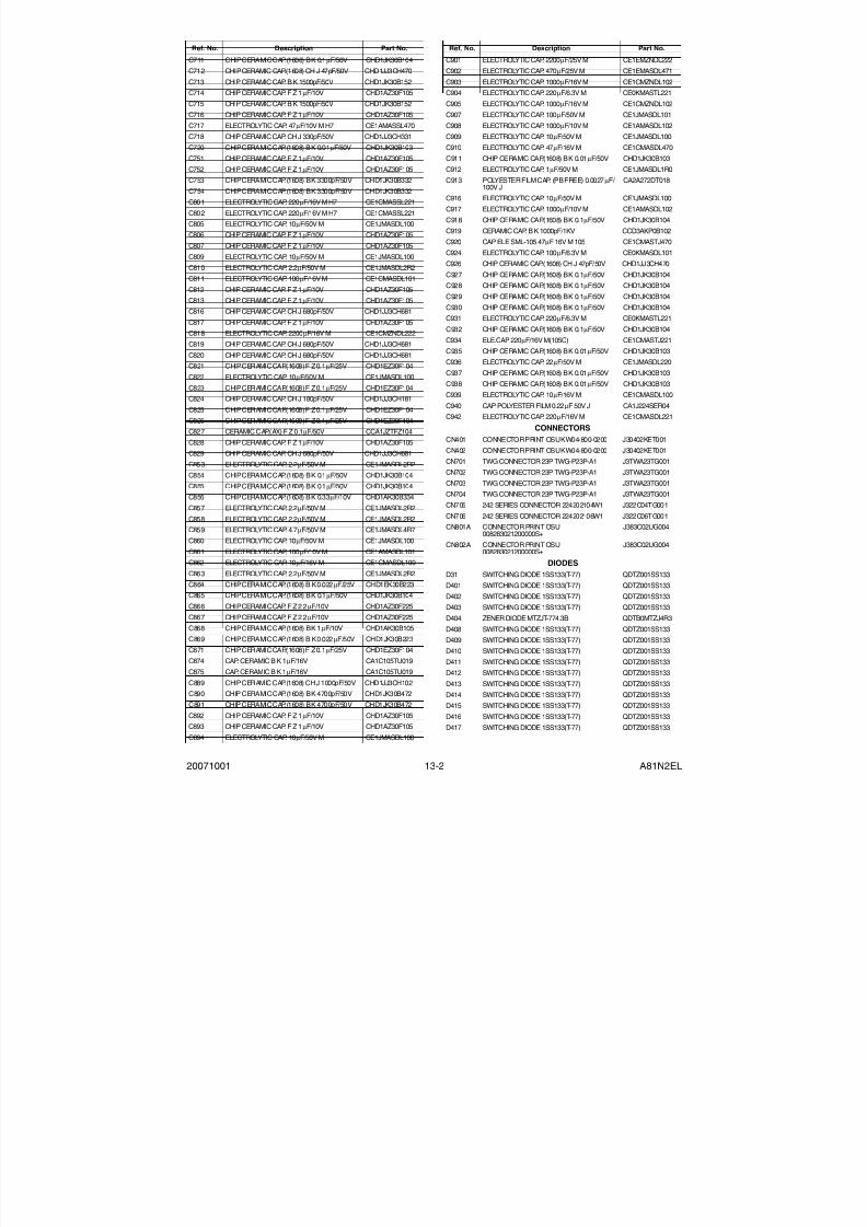
http://slidepdf.com/reader/full/sylvania-lc195sl8-lcd-tv-sm 54/6020071001 13-2 A81N2EL
C711 CHIP CERAMIC CAP.(1608) B K 0.1 µF/50V CHD1JK30B104
C712 CHIP CERAMIC CAP.(1608) CH J 47pF/50V CHD1JJ3CH470
C713 CHIP CERAMIC CAP. B K 1500pF/50V CHD1JK30B152C714 CHIP CERAMIC CAP. F Z 1 µF/10V CHD1AZ30F105
C715 CHIP CERAMIC CAP. B K 1500pF/50V CHD1JK30B152
C716 CHIP CERAMIC CAP. F Z 1 µF/10V CHD1AZ30F105
C717 ELECTROLYTIC CAP. 47 µF/10V M H7 CE1AMASSL470
C718 CHIP CERAMIC CAP. CH J 330pF/50V CHD1JJ3CH331
C720 CHIP CERAMIC CAP.(1608) B K 0.01 µF/50V CHD1JK30B103
C751 CHIP CERAMIC CAP. F Z 1 µF/10V CHD1AZ30F105
C752 CHIP CERAMIC CAP. F Z 1 µF/10V CHD1AZ30F105
C753 CHIP CERAMIC CAP.(1608) B K 3300pF/50V CHD1JK30B332
C754 CHIP CERAMIC CAP.(1608) B K 3300pF/50V CHD1JK30B332
C801 ELECTROLYTIC CAP. 220 µF/16V M H7 CE1CMASSL221
C802 ELECTROLYTIC CAP. 220 µF/16V M H7 CE1CMASSL221C805 ELECTROLYTIC CAP. 10 µF/50V M CE1JMASDL100
C806 CHIP CERAMIC CAP. F Z 1 µF/10V CHD1AZ30F105
C807 CHIP CERAMIC CAP. F Z 1 µF/10V CHD1AZ30F105
C809 ELECTROLYTIC CAP. 10 µF/50V M CE1JMASDL100
C810 ELECTROLYTIC CAP. 2.2 µF/50V M CE1JMASDL2R2
C811 ELECTROLYTIC CAP. 100 µF/16V M CE1CMASDL101
C812 CHIP CERAMIC CAP. F Z 1 µF/10V CHD1AZ30F105
C813 CHIP CERAMIC CAP. F Z 1 µF/10V CHD1AZ30F105C816 CHIP CERAMIC CAP. CH J 680pF/50V CHD1JJ3CH681
C817 CHIP CERAMIC CAP. F Z 1 µF/10V CHD1AZ30F105C818 ELECTROLYTIC CAP. 2200 µF/16V M CE1CMZNDL222
C819 CHIP CERAMIC CAP. CH J 680pF/50V CHD1JJ3CH681
C820 CHIP CERAMIC CAP. CH J 680pF/50V CHD1JJ3CH681C821 CHIP CERAMIC CAP.(1608) F Z 0.1 µF/25V CHD1EZ30F104
C822 ELECTROLYTIC CAP. 10 µF/50V M CE1JMASDL100
C823 CHIP CERAMIC CAP.(1608) F Z 0.1 µF/25V CHD1EZ30F104C824 CHIP CERAMIC CAP. CH J 180pF/50V CHD1JJ3CH181
C825 CHIP CERAMIC CAP.(1608) F Z 0.1 µF/25V CHD1EZ30F104
C826 CHIP CERAMIC CAP.(1608) F Z 0.1 µF/25V CHD1EZ30F104
C827 CERAMIC CAP.(AX) F Z 0.1 µF/50V CCA1JZTFZ104
C828 CHIP CERAMIC CAP. F Z 1 µF/10V CHD1AZ30F105
C829 CHIP CERAMIC CAP. CH J 680pF/50V CHD1JJ3CH681C853 ELECTROLYTIC CAP. 2.2 µF/50V M CE1JMASDL2R2
C854 CHIP CERAMIC CAP.(1608) B K 0.1 µF/50V CHD1JK30B104
C855 CHIP CERAMIC CAP.(1608) B K 0.1 µF/50V CHD1JK30B104
C856 CHIP CERAMIC CAP.(1608) B K 0.33 µF/10V CHD1AK30B334
C857 ELECTROLYTIC CAP. 2.2 µF/50V M CE1JMASDL2R2
C858 ELECTROLYTIC CAP. 2.2 µF/50V M CE1JMASDL2R2C859 ELECTROLYTIC CAP. 4.7 µF/50V M CE1JMASDL4R7
C860 ELECTROLYTIC CAP. 10 µF/50V M CE1JMASDL100
C861 ELECTROLYTIC CAP. 100 µF/10V M CE1AMASDL101C862 ELECTROLYTIC CAP. 10 µF/16V M CE1CMASDL100
C863 ELECTROLYTIC CAP. 2.2 µF/50V M CE1JMASDL2R2
C864 CHIP CERAMIC CAP.(1608) B K 0.022 µF/25V CHD1EK30B223C865 CHIP CERAMIC CAP.(1608) B K 0.1 µF/50V CHD1JK30B104
C866 CHIP CERAMIC CAP. F Z 2.2 µF/10V CHD1AZ30F225C867 CHIP CERAMIC CAP. F Z 2.2 µF/10V CHD1AZ30F225
C868 CHIP CERAMIC CAP.(1608) B K 1 µF/10V CHD1AK30B105
C869 CHIP CERAMIC CAP.(1608) B K 0.022 µF/50V CHD1JK30B223
C871 CHIP CERAMIC CAP.(1608) F Z 0.1 µF/25V CHD1EZ30F104
C874 CAP. CERAMIC B K 1 µF/16V CA1C105TU019
C875 CAP. CERAMIC B K 1 µF/16V CA1C105TU019
C889 CHIP CERAMIC CAP.(1608) CH J 1000pF/50V CHD1JJ3CH102C890 CHIP CERAMIC CAP.(1608) B K 4700pF/50V CHD1JK30B472
C891 CHIP CERAMIC CAP.(1608) B K 4700pF/50V CHD1JK30B472
C892 CHIP CERAMIC CAP. F Z 1 µF/10V CHD1AZ30F105C893 CHIP CERAMIC CAP. F Z 1 µF/10V CHD1AZ30F105
C894 ELECTROLYTIC CAP. 10 µF/50V M CE1JMASDL100
Ref. No. Description Part No.
C901 ELECTROLYTIC CAP. 2200 µF/25V M CE1EMZNDL222
C902 ELECTROLYTIC CAP. 470 µF/25V M CE1EMASDL471
C903 ELECTROLYTIC CAP. 1000 µF/16V M CE1CMZNDL102C904 ELECTROLYTIC CAP. 220 µF/6.3V M CE0KMASTL221
C905 ELECTROLYTIC CAP. 1000 µF/16V M CE1CMZNDL102
C907 ELECTROLYTIC CAP. 100 µF/50V M CE1JMASDL101
C908 ELECTROLYTIC CAP. 1000 µF/10V M CE1AMASDL102
C909 ELECTROLYTIC CAP. 10 µF/50V M CE1JMASDL100
C910 ELECTROLYTIC CAP. 47 µF/16V M CE1CMASDL470
C911 CHIP CERAMIC CAP.(1608) B K 0.01 µF/50V CHD1JK30B103
C912 ELECTROLYTIC CAP. 1 µF/50V M CE1JMASDL1R0
C913 POLYESTER FILM CAP. (PB FREE) 0.0027 µF/ 100V J
CA2A272DT018
C916 ELECTROLYTIC CAP. 10 µF/50V M CE1JMASDL100
C917 ELECTROLYTIC CAP. 1000 µF/10V M CE1AMASDL102
C918 CHIP CERAMIC CAP.(1608) B K 0.1 µF/50V CHD1JK30B104
C919 CERAMIC CAP. B K 1000pF/1KV CCD3AKP0B102
C920 CAP ELE SML-105 47 µF 16V M 105 CE1CMASTJ470
C924 ELECTROLYTIC CAP. 100 µF/6.3V M CE0KMASDL101
C926 CHIP CERAMIC CAP.(1608) CH J 47pF/50V CHD1JJ3CH470
C927 CHIP CERAMIC CAP.(1608) B K 0.1 µF/50V CHD1JK30B104C928 CHIP CERAMIC CAP.(1608) B K 0.1 µF/50V CHD1JK30B104
C929 CHIP CERAMIC CAP.(1608) B K 0.1 µF/50V CHD1JK30B104
C930 CHIP CERAMIC CAP.(1608) B K 0.1 µF/50V CHD1JK30B104C931 ELECTROLYTIC CAP. 220 µF/6.3V M CE0KMASTL221
C932 CHIP CERAMIC CAP.(1608) B K 0.1 µF/50V CHD1JK30B104
C934 ELE.CAP 220 µF/16V M(105C) CE1CMASTJ221
C935 CHIP CERAMIC CAP.(1608) B K 0.01 µF/50V CHD1JK30B103
C936 ELECTROLYTIC CAP. 22 µF/50V M CE1JMASDL220
C937 CHIP CERAMIC CAP.(1608) B K 0.01 µF/50V CHD1JK30B103
C938 CHIP CERAMIC CAP.(1608) B K 0.01 µF/50V CHD1JK30B103
C939 ELECTROLYTIC CAP. 10 µF/16V M CE1CMASDL100
C940 CAP POLYESTER FILM 0.22 µF 50V J CA1J224SER04C942 ELECTROLYTIC CAP. 220 µF/16V M CE1CMASDL221
CONNECTORSCN401 CONNECTOR PRINT OSU KW04-800-0200 J30402KET001
CN402 CONNECTOR PRINT OSU KW04-800-0200 J30402KET001
CN701 TWG CONNECTOR 23P TWG-P23P-A1 J3TWA23TG001
CN702 TWG CONNECTOR 23P TWG-P23P-A1 J3TWA23TG001
CN703 TWG CONNECTOR 23P TWG-P23P-A1 J3TWA23TG001
CN704 TWG CONNECTOR 23P TWG-P23P-A1 J3TWA23TG001
CN705 242 SERIES CONNECTOR 224202104W1 J322C04TG001
CN706 242 SERIES CONNECTOR 224202106W1 J322C06TG001CN801A CONNECTOR PRINT OSU
008283021200000S+J383C02UG004
CN802A CONNECTOR PRINT OSU008283021200000S+
J383C02UG004
DIODESD31 SWITCHING DIODE 1SS133(T-77) QDTZ001SS133
D401 SWITCHING DIODE 1SS133(T-77) QDTZ001SS133
D402 SWITCHING DIODE 1SS133(T-77) QDTZ001SS133
D403 SWITCHING DIODE 1SS133(T-77) QDTZ001SS133D404 ZENER DIODE MTZJT-774.3B QDTB0MTZJ4R3
D408 SWITCHING DIODE 1SS133(T-77) QDTZ001SS133D409 SWITCHING DIODE 1SS133(T-77) QDTZ001SS133
D410 SWITCHING DIODE 1SS133(T-77) QDTZ001SS133
D411 SWITCHING DIODE 1SS133(T-77) QDTZ001SS133D412 SWITCHING DIODE 1SS133(T-77) QDTZ001SS133
D413 SWITCHING DIODE 1SS133(T-77) QDTZ001SS133
D414 SWITCHING DIODE 1SS133(T-77) QDTZ001SS133D415 SWITCHING DIODE 1SS133(T-77) QDTZ001SS133
D416 SWITCHING DIODE 1SS133(T-77) QDTZ001SS133
D417 SWITCHING DIODE 1SS133(T-77) QDTZ001SS133
Ref. No. Description Part No.

7/21/2019 Sylvania Lc195sl8 Lcd Tv Sm
http://slidepdf.com/reader/full/sylvania-lc195sl8-lcd-tv-sm 55/6020071001 13-3 A81N2EL
D418 SWITCHING DIODE 1SS133(T-77) QDTZ001SS133
D419 SWITCHING DIODE 1SS133(T-77) QDTZ001SS133
D420 SWITCHING DIODE 1SS133(T-77) QDTZ001SS133D421 SWITCHING DIODE 1SS133(T-77) QDTZ001SS133
D422 SWITCHING DIODE 1SS133(T-77) QDTZ001SS133
D423 SWITCHING DIODE 1SS133(T-77) QDTZ001SS133
D501 SWITCHING DIODE 1SS133(T-77) QDTZ001SS133
D502 SWITCHING DIODE 1SS133(T-77) QDTZ001SS133
D503 SWITCHING DIODE 1SS133(T-77) QDTZ001SS133
D504 SWITCHING DIODE 1SS133(T-77) QDTZ001SS133
D507 SWITCHING DIODE 1SS133(T-77) QDTZ001SS133
D509 SWITCHING DIODE 1SS133(T-77) QDTZ001SS133
D510 SWITCHING DIODE 1SS133(T-77) QDTZ001SS133
D511 ZENER DIODE MTZJT-7739B QDTB00MTZJ39
D512 SWITCHING DIODE 1SS133(T-77) QDTZ001SS133D513 SWITCHING DIODE 1SS133(T-77) QDTZ001SS133
D516 SWITCHING DIODE 1SS133(T-77) QDTZ001SS133
D518 ZENER DIODE MTZJT-776.2B QDTB0MTZJ6R2
D519 SWITCHING DIODE 1SS133(T-77) QDTZ001SS133
D523 SWITCHING DIODE 1SS133(T-77) QDTZ001SS133
D524 SWITCHING DIODE 1SS133(T-77) QDTZ001SS133
D562 SWITCHING DIODE 1SS133(T-77) QDTZ001SS133
D563 SWITCHING DIODE 1SS133(T-77) QDTZ001SS133D568 SWITCHING DIODE 1SS133(T-77) QDTZ001SS133
D569 SWITCHING DIODE 1SS133(T-77) QDTZ001SS133D570 SWITCHING DIODE 1SS133(T-77) QDTZ001SS133
D605 # DIODE 1N5397-B NDLZ001N5397
D606 # DIODE 1N5397-B NDLZ001N5397D607 # DIODE 1N5397-B NDLZ001N5397
D608 # DIODE 1N5397-B NDLZ001N5397
D609 ZENER DIODE MTZJT-775.6B QDTB0MTZJ5R6D611 # ZENER DIODE MTZJT-7722B QDTB00MTZJ22
D612 SWITCHING DIODE 1SS133(T-77) QDTZ001SS133
D613 SWITCHING DIODE 1SS133(T-77) QDTZ001SS133
D614 SWITCHING DIODE 1SS133(T-77) QDTZ001SS133
D616 # ZENER DIODE MTZJT-7733B QDTB00MTZJ33
D624 # ZENER DIODE MTZJT-7739B QDTB00MTZJ39D702 ZENER DIODE MTZJT-773.9B QDTB0MTZJ3R9
D801 SWITCHING DIODE 1SS133(T-77) QDTZ001SS133
D802 ZENER DIODE MTZJT-7712B QDTB00MTZJ12
D901 SCHOTTKY BARRIER DIODE ERC84-009 QDLZERC84009
D902 RECTIFIER DIODE FR202-B/P NDQZ000FR202
D903 SCHOTTKY BARRIER DIODE ERC81-004 QDPZERC81004D904 ZENER DIODE MTZJT-7724B QDTB00MTZJ24
D906 SCHOTTKY BARRIER DIODE ERA81-004Q QDLZRA81004Q
D909 DIODE FR154 NDLZ000FR154D910 DIODE 1ZC43(Q) QDLZ001ZC43Q
D911 SCHOTTKY BARRIER DIODE ERC81-004 QDPZERC81004
D914 DIODE FR104-B NDLZ000FR104D915 PCB JUMPER D0.6-P5.0 JW5.0T
D916 SWITCHING DIODE 1SS133(T-77) QDTZ001SS133D917 SCHOTTKY BARRIER DIODE ERA81-004Q QDLZRA81004Q
D918 PCB JUMPER D0.6-P10.0 JW10.0T
D919 SWITCHING DIODE 1SS133(T-77) QDTZ001SS133
D922 ZENER DIODE MTZJT-775.6B QDTB0MTZJ5R6
D925 ZENER DIODE MTZJT-7724B QDTB00MTZJ24
D926 ZENER DIODE MTZJT-776.2B QDTB0MTZJ6R2
D927 SWITCHING DIODE 1SS133(T-77) QDTZ001SS133D928 ZENER DIODE MTZJT-7733B QDTB00MTZJ33
D929 SWITCHING DIODE 1SS133(T-77) QDTZ001SS133
D930 ZENER DIODE MTZJT-775.6B QDTB0MTZJ5R6D932 DIODE FR154 NDLZ000FR154
D933 ZENER DIODE MTZJT-775.6B QDTB0MTZJ5R6
Ref. No. Description Part No.
D934 SWITCHING DIODE 1SS133(T-77) QDTZ001SS133
D940 ZENER DIODE MTZJT-7710B QDTB00MTZJ10
D942 SWITCHING DIODE 1SS133(T-77) QDTZ001SS133D947 PCB JUMPER D0.6-P5.0 JW5.0T
D948 PCB JUMPER D0.6-P5.0 JW5.0T
D951 SWITCHING DIODE 1SS133(T-77) QDTZ001SS133
D952 SWITCHING DIODE 1SS133(T-77) QDTZ001SS133
D956 ZENER DIODE MTZJT-7712B QDTB00MTZJ12
D957 ZENER DIODE MTZJT-773.9B QDTB0MTZJ3R9
D962 SWITCHING DIODE 1SS133(T-77) QDTZ001SS133
D963 SWITCHING DIODE 1SS133(T-77) QDTZ001SS133
ICSIC31 IC VIF/SIF M61116FP TF0G QSZBA0SHT034IC61 IC EEPROM AT24C128N-10SU-1.8 S NSZBA0TAZ083
IC601 # PHOTO COUPLER LTV817MCF NPECLTV817MF
IC801 IC AN17812A QSZBA0SMS017
IC851 IC MTS DECORDER AN5832SA-E1V QSZBA0TMS003
IC852 IC SWITCHING TC4052BF(ELNF) QSZBA0TTS162
IC853 IC SWITCH TC4053BF(EL N F) QSZBA0TTS163
IC904 VOLTAGE REGULATOR PQ070XF01SZH QSZBA0SSH054IC905 IC VOLTAGE REGULATOR 5V KIA7805API/P NSZBA0SJY041
IC908 SHUNT REGULATOR KIA2431AP-AT/P NSZBA0TJY054
IC909 IC SHUNT REGULATOR KIA431-AT/P NSZBA0TJY036IC910 IC SHUNT REGULATOR KIA431-AT/P NSZBA0TJY036
IC911 IC SHUNT REGULATOR KIA431-AT/P NSZBA0TJY036
IC912 IC SHUNT REGULATOR KIA431-AT/P NSZBA0TJY036IC913 IC SHUNT REGULATOR KIA431-AT/P NSZBA0TJY036
COILSL21 PCB JUMPER D0.6-P5.0 JW5.0T
L22 INDUCTOR 100 µH-J-26T LLAXJATTU101L31 PCB JUMPER D0.6-P5.0 JW5.0T
L32 INDUCTOR 18 µH-J-26T LLAXJATTU180
L61 PCB JUMPER D0.6-P5.0 JW5.0TL63 PCB JUMPER D0.6-P5.0 JW5.0T
L66 INDUCTOR CHIP LK16081R0K-T 1.0 µH LLACKB3TU1R0
L401B POWER INDUCTER RCR1616-471K LLC471KSF009
L403 CHOKE COIL 22 µH-K LLBD00PKV021L601 # LINE FILTER 5.0MH 6Y075 LLBG00ZKT004
L701 PCB JUMPER D0.6-P5.0 JW5.0T
L702 INDUCTOR 22 µH-J-26T LLAXJATTU220
L851 PCB JUMPER D0.6-P5.0 JW5.0T
TRANSISTORSQ401 TRANSISTOR 2SA950-O (TE2 F T) QQS002SA950FQ402 TRANSISTOR KTC3199-GR-AT/P NQS4KTC3199P
Q403 TRANSISTOR KTC3199-GR-AT/P NQS4KTC3199P
Q404 TRANSISTOR KTA1267-GR-AT/P NQS1KTA1267PQ405 TRANSISTOR 2SC2120-Y(TE2 F T) QQSY2SC2120F
Q406 NPN TRANSISTOR POWER 2SC4881F HFEMAX320
QQWZ2SC4881F
Q407 TRANSISTOR KTC3199-GR-AT/P NQS4KTC3199P
Q408 # FET MOS SMD HAT2215R01-EL-E QF2ZHAT2215RQ409 TRANSISTOR KTC3199-GR-AT/P NQS4KTC3199P
Q410 TRANSISTOR KTC3199-GR-AT/P NQS4KTC3199P
Q411 TRANSISTOR KTA1267-GR-AT/P NQS1KTA1267PQ412 TRANSISTOR KTC3199-GR-AT/P NQS4KTC3199P
Q501 TRANSISTOR KTC3199-GR-AT/P NQS4KTC3199P
Q601 # FET MOS 2SK3563(Q) QFWZ2SK3563Q
Q603 # TRANSISTOR 2SC2120-Y(TE2 F T) QQSY2SC2120F
Q707 TRANSISTOR KTC3199-GR-AT/P NQS4KTC3199P
Q708 TRANSISTOR KTC3199-GR-AT/P NQS4KTC3199P
Q709 TRANSISTOR KTC3199-GR-AT/P NQS4KTC3199P
Q802 TRANSISTOR KTC3199-GR-AT/P NQS4KTC3199P
Q901 TRANSISTOR 2SC2120-Y(TE2 F T) QQSY2SC2120F
Ref. No. Description Part No.
7/21/2019 Sylvania Lc195sl8 Lcd Tv Sm
http://slidepdf.com/reader/full/sylvania-lc195sl8-lcd-tv-sm 56/6020071001 13-4 A81N2EL
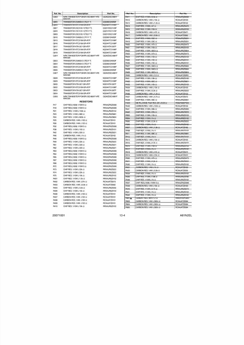
Q902 NPN TRANSISTOR POWER 2SC4881F HFEMAX320
QQWZ2SC4881F
Q905 TRANSISTOR 2SA950-O (TE2 F T) QQS002SA950F
Q906 TRANSISTOR KTC3199-GR-AT/P NQS4KTC3199P
Q907 TRANSISTOR 2SC2120-Y(TE2 F T) QQSY2SC2120FQ908 TRANSISTOR 2SC2120-Y(TE2 F T) QQSY2SC2120F
Q909 TRANSISTOR 2SC2120-Y(TE2 F T) QQSY2SC2120F
Q910 TRANSISTOR 2SA950-O (TE2 F T) QQS002SA950FQ913 TRANSISTOR KTC3199-GR-AT/P NQS4KTC3199P
Q916 TRANSISTOR KTC3199-GR-AT/P NQS4KTC3199P
Q917 TRANSISTOR KTA1267-GR-AT/P NQS1KTA1267PQ918 TRANSISTOR KTC3199-GR-AT/P NQS4KTC3199P
Q919 TRANSISTOR KTC3199-GR-AT/P NQS4KTC3199P
Q922 NPN TRANSISTOR POWER 2SC4881F HFEMAX320
QQWZ2SC4881F
Q923 TRANSISTOR 2SA950-O (TE2 F T) QQS002SA950FQ924 TRANSISTOR 2SA950-O (TE2 F T) QQS002SA950F
Q925 TRANSISTOR KTC3199-GR-AT/P NQS4KTC3199P
Q926 TRANSISTOR 2SA950-O (TE2 F T) QQS002SA950F
Q927 NPN TRANSISTOR POWER 2SC4881F HFEMAX320
QQWZ2SC4881F
Q928 TRANSISTOR KTC3199-GR-AT/P NQS4KTC3199PQ929 TRANSISTOR KTC3199-GR-AT/P NQS4KTC3199P
Q930 TRANSISTOR KTA1267-GR-AT/P NQS1KTA1267PQ932 TRANSISTOR KTC3199-GR-AT/P NQS4KTC3199P
Q933 TRANSISTOR KTA1267-GR-AT/P NQS1KTA1267P
Q934 TRANSISTOR KTC3199-GR-AT/P NQS4KTC3199P
Q935 NPN TRANSISTOR POWER 2SC4881F HFEMAX320
QQWZ2SC4881F
RESISTORSR17 CHIP RES.(1608) 1/10W 0 Ω RRXAZR5Z0000
R18 CHIP RES.(1608) 1/10W 0 Ω RRXAZR5Z0000
R21 CHIP RES. 1/10W J 150k Ω RRXAJR5Z0154
R23 CHIP RES. 1/10W J 680 Ω RRXAJR5Z0681R24 CHIP RES. 1/10W J 820k Ω RRXAJR5Z0824
R25 CARBON RES. 1/4W J 100 Ω RCX4JATZ0101
R26 CARBON RES. 1/4W J 100 Ω RCX4JATZ0101R32 CHIP RES.(1608) 1/10W 0 Ω RRXAZR5Z0000
R38 CHIP RES. 1/10W J 100 Ω RRXAJR5Z0101
R42 CHIP RES. 1/10W J 220 Ω RRXAJR5Z0221R46 CARBON RES. 1/4W J 1k Ω RCX4JATZ0102
R48 CHIP RES.(1608) 1/10W 0 Ω RRXAZR5Z0000
R49 CHIP RES. 1/10W J 22k Ω RRXAJR5Z0223
R61 CHIP RES. 1/10W J 220 Ω RRXAJR5Z0221
R62 CHIP RES. 1/10W J 220 Ω RRXAJR5Z0221
R63 CHIP RES.(1608) 1/10W 0 Ω RRXAZR5Z0000
R64 CHIP RES.(1608) 1/10W 0 Ω RRXAZR5Z0000
R65 CHIP RES.(1608) 1/10W 0 Ω RRXAZR5Z0000
R67 CHIP RES.(1608) 1/10W 0 Ω RRXAZR5Z0000
R68 CHIP RES.(1608) 1/10W 0 Ω RRXAZR5Z0000
R72 CHIP RES.(1608) 1/10W 0 Ω RRXAZR5Z0000
R73 CHIP RES. 1/10W J 22k Ω RRXAJR5Z0223R74 CHIP RES. 1/10W J 22k Ω RRXAJR5Z0223
R75 CHIP RES. 1/10W J 10k Ω RRXAJR5Z0103
R401 CHIP RES. 1/10W J 1.5k Ω RRXAJR5Z0152R402 CARBON RES. 1/4W J 27k Ω RCX4JATZ0273
R403 CARBON RES. 1/4W J 5.6k Ω RCX4JATZ0562
R404 CHIP RES. 1/10W J 3.3k Ω RRXAJR5Z0332
R405 CHIP RES. 1/10W J 10k Ω RRXAJR5Z0103
R406 CARBON RES. 1/4W J 100 Ω RCX4JATZ0101
R407 CARBON RES. 1/4W J 100 Ω RCX4JATZ0101
R408 CARBON RES. 1/4W J 100 Ω RCX4JATZ0101
R409 CARBON RES. 1/4W J 100 Ω RCX4JATZ0101
R410 CHIP RES. 1/10W J 10k Ω RRXAJR5Z0103
Ref. No. Description Part No.
R411 CHIP RES. 1/10W J 3.3k Ω RRXAJR5Z0332
R412 CARBON RES. 1/4W J 10k Ω RCX4JATZ0103
R413 CARBON RES. 1/4W J 1.2k Ω RCX4JATZ0122R414 CHIP RES. 1/10W J 47 Ω RRXAJR5Z0470
R415 CHIP RES. 1/10W J 10k Ω RRXAJR5Z0103
R416 CARBON RES. 1/4W J 470 Ω RCX4JATZ0471
R417 CARBON RES. 1/4W J 5.6k Ω RCX4JATZ0562
R418 CHIP RES. 1/10W J 330 Ω RRXAJR5Z0331
R419 CHIP RES. 1/10W J 330 Ω RRXAJR5Z0331
R420 CHIP RES. 1/10W J 47k Ω RRXAJR5Z0473
R421 CHIP RES. 1/10W J 10k Ω RRXAJR5Z0103
R422 CHIP RES. 1/10W J 820k Ω RRXAJR5Z0824
R423 CHIP RES. 1/10W J 47k Ω RRXAJR5Z0473
R424 CHIP RES. 1/10W J 10k Ω RRXAJR5Z0103
R425 CHIP RES. 1/10W J 100 Ω RRXAJR5Z0101R426 CHIP RES. 1/10W J 100 Ω RRXAJR5Z0101
R427 CHIP RES. 1/10W J 560k Ω RRXAJR5Z0564
R428 CHIP RES. 1/10W J 560k Ω RRXAJR5Z0564
R429 CHIP RES. 1/10W J 820k Ω RRXAJR5Z0824
R430 CARBON RES. 1/4W J 3.3 Ω RCX4JATZ03R3
R431 CHIP RES. 1/10W J 18k Ω RRXAJR5Z0183
R432 CHIP RES. 1/10W J 820 Ω RRXAJR5Z0821
R433 CHIP RES. 1/10W J 10k Ω RRXAJR5Z0103R434 CARBON RES. 1/4W J 10k Ω RCX4JATZ0103
R435 CHIP RES. 1/10W J 2.2k Ω RRXAJR5Z0222R436 CARBON RES. 1/4W J 1.2k Ω RCX4JATZ0122
R437 CARBON RES. 1/4W J 4.7k Ω RCX4JATZ0472
R438 CHIP RES. 1/10W J 560 Ω RRXAJR5Z0561R439 METAL OXIDE FILM RES. 2W J 0.68 Ω RN02R68DP004
R440 CARBON RES. 1/4W J 100k Ω RCX4JATZ0104
R441 CHIP RES. 1/10W J 39k Ω RRXAJR5Z0393R442 CHIP RES. 1/10W J 22k Ω RRXAJR5Z0223
R503 CHIP RES. 1/10W J 10k Ω RRXAJR5Z0103
R504 CHIP RES. 1/10W J 1k Ω RRXAJR5Z0102
R505 CHIP RES. 1/10W J 2.2k Ω RRXAJR5Z0222
R506 CHIP RES. 1/10W J 1k Ω RRXAJR5Z0102
R507 CARBON RES. 1/4W J 1.8k Ω RCX4JATZ0182R508 CHIP RES. 1/10W J 1k Ω RRXAJR5Z0102
R511 CHIP RES. 1/10W J 680 Ω RRXAJR5Z0681
R512 CHIP RES. 1/10W J 1k Ω RRXAJR5Z0102
R513 CARBON RES. 1/4W J 10k Ω RCX4JATZ0103
R515 CHIP RES. 1/10W J 2.7k Ω RRXAJR5Z0272
R516 CHIP RES. 1/10W J 15k Ω RRXAJR5Z0153R517 CHIP RES. 1/10W J 1k Ω RRXAJR5Z0102
R518 CARBON RES. 1/4W J 47k Ω RCX4JATZ0473
R519 CARBON RES. 1/4W J 22k Ω RCX4JATZ0223R520 CHIP RES. 1/10W J 47k Ω RRXAJR5Z0473
R521 CHIP RES. 1/10W J 2.2k Ω RRXAJR5Z0222
R530 CHIP RES. 1/10W J 1k Ω RRXAJR5Z0102R531 CARBON RES. 1/4W J 1k Ω RCX4JATZ0102
R533 CARBON RES. 1/4W J 3.3k Ω RCX4JATZ0332R534 CHIP RES. 1/10W J 1k Ω RRXAJR5Z0102
R535 CHIP RES. 1/10W J 1.8k Ω RRXAJR5Z0182
R536 CHIP RES. 1/10W J 1k Ω RRXAJR5Z0102
R537 CHIP RES.(1608) 1/10W 0 Ω RRXAZR5Z0000
R539 CARBON RES. 1/4W J 18k Ω RCX4JATZ0183
R540 CHIP RES. 1/10W J 2.7k Ω RRXAJR5Z0272
R541 CHIP RES. 1/10W J 1k Ω RRXAJR5Z0102R542 CHIP RES. 1/10W J 1k Ω RRXAJR5Z0102
R601 # CEMENT RES. 3W K 1.2 Ω RW031R2PG007
R603 CARBON RES. 1/4W J 390k Ω RCX4JATZ0394R604 CARBON RES. 1/4W J 390k Ω RCX4JATZ0394
R605 CARBON RES. 1/4W J 390k Ω RCX4JATZ0394
Ref. No. Description Part No.
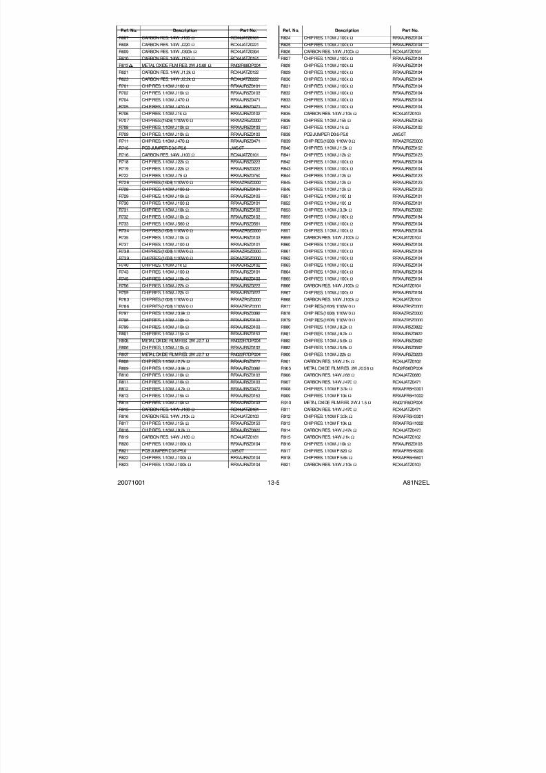
7/21/2019 Sylvania Lc195sl8 Lcd Tv Sm
http://slidepdf.com/reader/full/sylvania-lc195sl8-lcd-tv-sm 57/6020071001 13-5 A81N2EL
R607 CARBON RES. 1/4W J 180 Ω RCX4JATZ0181
R608 CARBON RES. 1/4W J 220 Ω RCX4JATZ0221
R609 CARBON RES. 1/4W J 390k Ω RCX4JATZ0394R610 CARBON RES. 1/4W J 150 Ω RCX4JATZ0151
R613 # METAL OXIDE FILM RES. 2W J 0.68 Ω RN02R68DP004
R621 CARBON RES. 1/4W J 1.2k Ω RCX4JATZ0122
R623 CARBON RES. 1/4W J 2.2k Ω RCX4JATZ0222
R701 CHIP RES. 1/10W J 100 Ω RRXAJR5Z0101
R702 CHIP RES. 1/10W J 10k Ω RRXAJR5Z0103
R704 CHIP RES. 1/10W J 470 Ω RRXAJR5Z0471
R705 CHIP RES. 1/10W J 470 Ω RRXAJR5Z0471
R706 CHIP RES. 1/10W J 1k Ω RRXAJR5Z0102
R707 CHIP RES.(1608) 1/10W 0 Ω RRXAZR5Z0000
R708 CHIP RES. 1/10W J 10k Ω RRXAJR5Z0103
R709 CHIP RES. 1/10W J 10k Ω RRXAJR5Z0103R711 CHIP RES. 1/10W J 470 Ω RRXAJR5Z0471
R715 PCB JUMPER D0.6-P5.0 JW5.0T
R716 CARBON RES. 1/4W J 100 Ω RCX4JATZ0101
R718 CHIP RES. 1/10W J 22k Ω RRXAJR5Z0223
R719 CHIP RES. 1/10W J 22k Ω RRXAJR5Z0223
R722 CHIP RES. 1/10W J 75 Ω RRXAJR5Z0750
R726 CHIP RES.(1608) 1/10W 0 Ω RRXAZR5Z0000
R728 CHIP RES. 1/10W J 100 Ω RRXAJR5Z0101R729 CHIP RES. 1/10W J 10k Ω RRXAJR5Z0103
R730 CHIP RES. 1/10W J 100 Ω RRXAJR5Z0101R731 CHIP RES. 1/10W J 10k Ω RRXAJR5Z0103
R732 CHIP RES. 1/10W J 10k Ω RRXAJR5Z0103
R733 CHIP RES. 1/10W J 560 Ω RRXAJR5Z0561R734 CHIP RES.(1608) 1/10W 0 Ω RRXAZR5Z0000
R735 CHIP RES. 1/10W J 10k Ω RRXAJR5Z0103
R737 CHIP RES. 1/10W J 100 Ω RRXAJR5Z0101R738 CHIP RES.(1608) 1/10W 0 Ω RRXAZR5Z0000
R739 CHIP RES.(1608) 1/10W 0 Ω RRXAZR5Z0000
R740 CHIP RES. 1/10W J 1k Ω RRXAJR5Z0102
R743 CHIP RES. 1/10W J 100 Ω RRXAJR5Z0101
R745 CHIP RES. 1/10W J 10k Ω RRXAJR5Z0103
R756 CHIP RES. 1/10W J 22k Ω RRXAJR5Z0223R759 CHIP RES. 1/10W J 22k Ω RRXAJR5Z0223
R783 CHIP RES.(1608) 1/10W 0 Ω RRXAZR5Z0000
R786 CHIP RES.(1608) 1/10W 0 Ω RRXAZR5Z0000
R797 CHIP RES. 1/10W J 3.9k Ω RRXAJR5Z0392
R798 CHIP RES. 1/10W J 10k Ω RRXAJR5Z0103
R799 CHIP RES. 1/10W J 10k Ω RRXAJR5Z0103R801 CHIP RES. 1/10W J 15k Ω RRXAJR5Z0153
R805 METAL OXIDE FILM RES. 2W J 2.7 Ω RN022R7DP004
R806 CHIP RES. 1/10W J 10k Ω RRXAJR5Z0103R807 METAL OXIDE FILM RES. 2W J 2.7 Ω RN022R7DP004
R808 CHIP RES. 1/10W J 2.7k Ω RRXAJR5Z0272
R809 CHIP RES. 1/10W J 3.9k Ω RRXAJR5Z0392R810 CHIP RES. 1/10W J 10k Ω RRXAJR5Z0103
R811 CHIP RES. 1/10W J 10k Ω RRXAJR5Z0103R812 CHIP RES. 1/10W J 4.7k Ω RRXAJR5Z0472
R813 CHIP RES. 1/10W J 15k Ω RRXAJR5Z0153
R814 CHIP RES. 1/10W J 10k Ω RRXAJR5Z0103
R815 CARBON RES. 1/4W J 180 Ω RCX4JATZ0181
R816 CARBON RES. 1/4W J 10k Ω RCX4JATZ0103
R817 CHIP RES. 1/10W J 15k Ω RRXAJR5Z0153
R818 CHIP RES. 1/10W J 8.2k Ω RRXAJR5Z0822R819 CARBON RES. 1/4W J 180 Ω RCX4JATZ0181
R820 CHIP RES. 1/10W J 100k Ω RRXAJR5Z0104
R821 PCB JUMPER D0.6-P5.0 JW5.0TR822 CHIP RES. 1/10W J 100k Ω RRXAJR5Z0104
R823 CHIP RES. 1/10W J 100k Ω RRXAJR5Z0104
Ref. No. Description Part No.
R824 CHIP RES. 1/10W J 100k Ω RRXAJR5Z0104
R825 CHIP RES. 1/10W J 100k Ω RRXAJR5Z0104
R826 CARBON RES. 1/4W J 100k Ω RCX4JATZ0104R827 CHIP RES. 1/10W J 100k Ω RRXAJR5Z0104
R828 CHIP RES. 1/10W J 100k Ω RRXAJR5Z0104
R829 CHIP RES. 1/10W J 100k Ω RRXAJR5Z0104
R830 CHIP RES. 1/10W J 100k Ω RRXAJR5Z0104
R831 CHIP RES. 1/10W J 100k Ω RRXAJR5Z0104
R832 CHIP RES. 1/10W J 100k Ω RRXAJR5Z0104
R833 CHIP RES. 1/10W J 100k Ω RRXAJR5Z0104
R834 CHIP RES. 1/10W J 100k Ω RRXAJR5Z0104
R835 CARBON RES. 1/4W J 10k Ω RCX4JATZ0103
R836 CHIP RES. 1/10W J 15k Ω RRXAJR5Z0153
R837 CHIP RES. 1/10W J 1k Ω RRXAJR5Z0102
R838 PCB JUMPER D0.6-P5.0 JW5.0TR839 CHIP RES.(1608) 1/10W 0 Ω RRXAZR5Z0000
R840 CHIP RES. 1/10W J 1.5k Ω RRXAJR5Z0152
R841 CHIP RES. 1/10W J 12k Ω RRXAJR5Z0123
R842 CHIP RES. 1/10W J 100k Ω RRXAJR5Z0104
R843 CHIP RES. 1/10W J 100k Ω RRXAJR5Z0104
R844 CHIP RES. 1/10W J 12k Ω RRXAJR5Z0123
R845 CHIP RES. 1/10W J 12k Ω RRXAJR5Z0123
R846 CHIP RES. 1/10W J 12k Ω RRXAJR5Z0123R851 CHIP RES. 1/10W J 100 Ω RRXAJR5Z0101
R852 CHIP RES. 1/10W J 100 Ω RRXAJR5Z0101R853 CHIP RES. 1/10W J 3.3k Ω RRXAJR5Z0332
R855 CHIP RES. 1/10W J 180k Ω RRXAJR5Z0184
R856 CHIP RES. 1/10W J 100k Ω RRXAJR5Z0104R857 CHIP RES. 1/10W J 100k Ω RRXAJR5Z0104
R859 CARBON RES. 1/4W J 100k Ω RCX4JATZ0104
R860 CHIP RES. 1/10W J 100k Ω RRXAJR5Z0104R861 CHIP RES. 1/10W J 100k Ω RRXAJR5Z0104
R862 CHIP RES. 1/10W J 100k Ω RRXAJR5Z0104
R863 CHIP RES. 1/10W J 100k Ω RRXAJR5Z0104
R864 CHIP RES. 1/10W J 100k Ω RRXAJR5Z0104
R865 CHIP RES. 1/10W J 100k Ω RRXAJR5Z0104
R866 CARBON RES. 1/4W J 100k Ω RCX4JATZ0104R867 CHIP RES. 1/10W J 100k Ω RRXAJR5Z0104
R868 CARBON RES. 1/4W J 100k Ω RCX4JATZ0104
R877 CHIP RES.(1608) 1/10W 0 Ω RRXAZR5Z0000
R878 CHIP RES.(1608) 1/10W 0 Ω RRXAZR5Z0000
R879 CHIP RES.(1608) 1/10W 0 Ω RRXAZR5Z0000
R880 CHIP RES. 1/10W J 8.2k Ω RRXAJR5Z0822R881 CHIP RES. 1/10W J 8.2k Ω RRXAJR5Z0822
R882 CHIP RES. 1/10W J 5.6k Ω RRXAJR5Z0562
R883 CHIP RES. 1/10W J 5.6k Ω RRXAJR5Z0562R900 CHIP RES. 1/10W J 22k Ω RRXAJR5Z0223
R901 CARBON RES. 1/4W J 1k Ω RCX4JATZ0102
R905 METAL OXIDE FILM RES. 2W J 0.56 Ω RN02R56DP004R906 CARBON RES. 1/4W J 68 Ω RCX4JATZ0680
R907 CARBON RES. 1/4W J 470 Ω RCX4JATZ0471R908 CHIP RES. 1/10W F 3.3k Ω RRXAFR5H3301
R909 CHIP RES. 1/10W F 10k Ω RRXAFR5H1002
R910 METAL OXIDE FILM RES. 2W J 1.5 Ω RN021R5DP004
R911 CARBON RES. 1/4W J 470 Ω RCX4JATZ0471
R912 CHIP RES. 1/10W F 3.3k Ω RRXAFR5H3301
R913 CHIP RES. 1/10W F 10k Ω RRXAFR5H1002
R914 CARBON RES. 1/4W J 47k Ω RCX4JATZ0473R915 CARBON RES. 1/4W J 1k Ω RCX4JATZ0102
R916 CHIP RES. 1/10W J 10k Ω RRXAJR5Z0103
R917 CHIP RES. 1/10W F 820 Ω RRXAFR5H8200R918 CHIP RES. 1/10W F 5.6k Ω RRXAFR5H5601
R921 CARBON RES. 1/4W J 10k Ω RCX4JATZ0103
Ref. No. Description Part No.
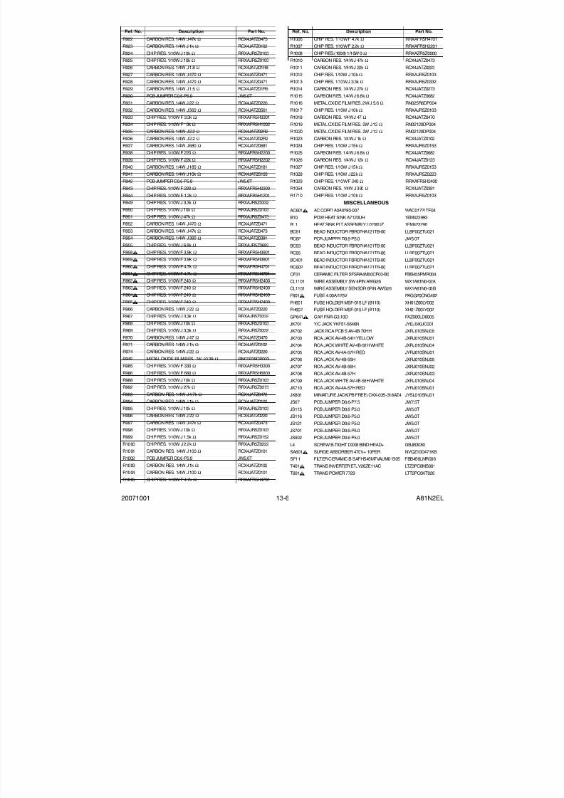
7/21/2019 Sylvania Lc195sl8 Lcd Tv Sm
http://slidepdf.com/reader/full/sylvania-lc195sl8-lcd-tv-sm 58/6020071001 13-6 A81N2EL
R922 CARBON RES. 1/4W J 47k Ω RCX4JATZ0473
R923 CARBON RES. 1/4W J 1k Ω RCX4JATZ0102
R924 CHIP RES. 1/10W J 10k Ω RRXAJR5Z0103R925 CHIP RES. 1/10W J 10k Ω RRXAJR5Z0103
R926 CARBON RES. 1/4W J 1.8 Ω RCX4JATZ01R8
R927 CARBON RES. 1/4W J 470 Ω RCX4JATZ0471
R928 CARBON RES. 1/4W J 470 Ω RCX4JATZ0471
R929 CARBON RES. 1/4W J 1.5 Ω RCX4JATZ01R5
R930 PCB JUMPER D0.6-P5.0 JW5.0T
R931 CARBON RES. 1/4W J 22 Ω RCX4JATZ0220
R932 CARBON RES. 1/4W J 560 Ω RCX4JATZ0561
R933 CHIP RES. 1/10W F 3.3k Ω RRXAFR5H3301
R934 CHIP RES. 1/10W F 10k Ω RRXAFR5H1002
R935 CARBON RES. 1/4W J 2.2 Ω RCX4JATZ02R2
R936 CARBON RES. 1/4W J 2.2 Ω RCX4JATZ02R2R937 CARBON RES. 1/4W J 680 Ω RCX4JATZ0681
R938 CHIP RES. 1/10W F 220 Ω RRXAFR5H2200
R939 CHIP RES. 1/10W F 22k Ω RRXAFR5H2202
R940 CARBON RES. 1/4W J 180 Ω RCX4JATZ0181
R941 CARBON RES. 1/4W J 10k Ω RCX4JATZ0103
R942 PCB JUMPER D0.6-P5.0 JW5.0T
R943 CHIP RES. 1/10W F 220 Ω RRXAFR5H2200
R944 CHIP RES. 1/10W F 1.2k Ω RRXAFR5H1201R949 CHIP RES. 1/10W J 3.3k Ω RRXAJR5Z0332
R950 CHIP RES. 1/10W J 10k Ω RRXAJR5Z0103R951 CHIP RES. 1/10W J 47k Ω RRXAJR5Z0473
R952 CARBON RES. 1/4W J 470 Ω RCX4JATZ0471
R953 CARBON RES. 1/4W J 47k Ω RCX4JATZ0473R954 CARBON RES. 1/4W J 390 Ω RCX4JATZ0391
R955 CHIP RES. 1/10W J 6.8k Ω RRXAJR5Z0682
R958 # CHIP RES. 1/10W F 3.9k Ω RRXAFR5H3901R959 # CHIP RES. 1/10W F 3.9k Ω RRXAFR5H3901
R960 # CHIP RES. 1/10W F 4.7k Ω RRXAFR5H4701
R961 # CHIP RES. 1/10W F 4.7k Ω RRXAFR5H4701
R962 # CHIP RES. 1/10W F 240 Ω RRXAFR5H2400
R963 # CHIP RES. 1/10W F 240 Ω RRXAFR5H2400
R964 # CHIP RES. 1/10W F 240 Ω RRXAFR5H2400R965 # CHIP RES. 1/10W F 240 Ω RRXAFR5H2400
R966 CARBON RES. 1/4W J 22 Ω RCX4JATZ0220
R967 CHIP RES. 1/10W J 3.3k Ω RRXAJR5Z0332
R968 CHIP RES. 1/10W J 10k Ω RRXAJR5Z0103
R969 CHIP RES. 1/10W J 3.3k Ω RRXAJR5Z0332
R970 CARBON RES. 1/4W J 47 Ω RCX4JATZ0470R971 CARBON RES. 1/4W J 1k Ω RCX4JATZ0102
R974 CARBON RES. 1/4W J 22 Ω RCX4JATZ0220
R982 METAL OXIDE FILM RES. 1W J 0.39 Ω RN01R39DP003R985 CHIP RES. 1/10W F 330 Ω RRXAFR5H3300
R986 CHIP RES. 1/10W F 680 Ω RRXAFR5H6800
R988 CHIP RES. 1/10W J 10k Ω RRXAJR5Z0103R992 CHIP RES. 1/10W J 27k Ω RRXAJR5Z0273
R993 CARBON RES. 1/4W J 4.7k Ω RCX4JATZ0472R994 CARBON RES. 1/4W J 1k Ω RCX4JATZ0102
R995 CHIP RES. 1/10W J 10k Ω RRXAJR5Z0103
R996 CARBON RES. 1/4W J 22 Ω RCX4JATZ0220
R997 CARBON RES. 1/4W J 47k Ω RCX4JATZ0473
R998 CHIP RES. 1/10W J 10k Ω RRXAJR5Z0103
R999 CHIP RES. 1/10W J 1.5k Ω RRXAJR5Z0152
R1000 CHIP RES. 1/10W J 2.2k Ω RRXAJR5Z0222R1001 CARBON RES. 1/4W J 100 Ω RCX4JATZ0101
R1002 PCB JUMPER D0.6-P5.0 JW5.0T
R1003 CARBON RES. 1/4W J 1k Ω RCX4JATZ0102R1004 CARBON RES. 1/4W J 100 Ω RCX4JATZ0101
R1005 CHIP RES. 1/10W F 4.7k Ω RRXAFR5H4701
Ref. No. Description Part No.
R1006 CHIP RES. 1/10W F 4.7k Ω RRXAFR5H4701
R1007 CHIP RES. 1/10W F 2.2k Ω RRXAFR5H2201
R1008 CHIP RES.(1608) 1/10W 0 Ω RRXAZR5Z0000R1010 CARBON RES. 1/4W J 47k Ω RCX4JATZ0473
R1011 CARBON RES. 1/4W J 22k Ω RCX4JATZ0223
R1012 CHIP RES. 1/10W J 10k Ω RRXAJR5Z0103
R1013 CHIP RES. 1/10W J 3.3k Ω RRXAJR5Z0332
R1014 CARBON RES. 1/4W J 27k Ω RCX4JATZ0273
R1015 CARBON RES. 1/4W J 6.8k Ω RCX4JATZ0682
R1016 METAL OXIDE FILM RES. 2W J 5.6 Ω RN025R6DP004
R1017 CHIP RES. 1/10W J 10k Ω RRXAJR5Z0103
R1018 CARBON RES. 1/4W J 47 Ω RCX4JATZ0470
R1019 METAL OXIDE FILM RES. 2W J 12 Ω RN02120DP004
R1020 METAL OXIDE FILM RES. 2W J 12 Ω RN02120DP004
R1023 CARBON RES. 1/4W J 1k Ω RCX4JATZ0102R1024 CHIP RES. 1/10W J 15k Ω RRXAJR5Z0153
R1025 CARBON RES. 1/4W J 6.8k Ω RCX4JATZ0682
R1026 CARBON RES. 1/4W J 12k Ω RCX4JATZ0123
R1027 CHIP RES. 1/10W J 15k Ω RRXAJR5Z0153
R1028 CHIP RES. 1/10W J 22k Ω RRXAJR5Z0223
R1029 CHIP RES. 1/10W F 240 Ω RRXAFR5H2400
R1054 CARBON RES. 1/4W J 390 Ω RCX4JATZ0391
R1710 CHIP RES. 1/10W J 10k Ω RRXAJR5Z0103MISCELLANEOUS
AC601 # AC CORD A0A0280-007 WAC0172LTE04
B10 POW HEAT SINK A7120UH 1EM423993B11 HEAT SINK PLT ASSEMBLY L0700UZ 1EM423290
BC61 BEAD INDUCTOR FBR07HA121TB-00 LLBF00ZTU021
BC62 PCB JUMPER D0.6-P5.0 JW5.0T
BC63 BEAD INDUCTOR FBR07HA121TB-00 LLBF00ZTU021
BC65 BEAD INDUCTOR FBR07HA121TB-00 LLBF00ZTU021
BC401 BEAD INDUCTOR FBR07HA121TB-00 LLBF00ZTU021
BC602 BEAD INDUCTOR FBR07HA121TB-00 LLBF00ZTU021
CF31 CERAMIC FILTER SFSRA4M50CF00-B0 FBB455PMR004
CL1101 WIRE ASSEMBLY SW 4PIN AWG26 WX1A81N0-02ACL1151 WIRE ASSEMBLY SENSOR 6PIN AWG26 WX1A81N0-03B
F601 # FUSE 4.00A/125V PAGG20CNG402FH601 FUSE HOLDER MSF-015 LF (B110) XH01Z00LY002FH602 FUSE HOLDER MSF-015 LF (B110) XH01Z00LY002
GP641 # GAP. FNR-G3.10D FAZ000LD6005
JK701 Y/C JACK YKF51-5646N JYEJ040JC001JK702 JACK RCA PCB S AV-4B-70HH JXRJ010SNJ06
JK703 RCA JACK AV-4B-54H YELLOW JXRJ010SNJ01
JK704 RCA JACK WHITE AV-4B-58H WHITE JXRJ010SNJ04
JK705 RCA JACK AV-4A-57H RED JYRJ010SNJ01
JK706 RCA JACK AV-4B-55H JXRJ010SNJ05
JK707 RCA JACK AV-4B-56H JXRJ010SNJ02
JK708 RCA JACK AV-4B-57H JXRJ010SNJ03
JK709 RCA JACK WHITE AV-4B-58H WHITE JXRJ010SNJ04
JK710 RCA JACK AV-4A-57H RED JYRJ010SNJ01
JK801 MINIATURE JACK(PB FREE) CKX-035-318AZ4 JYSL010SNJ01JS67 PCB JUMPER D0.6-P7.5 JW7.5T
JS115 PCB JUMPER D0.6-P5.0 JW5.0TJS116 PCB JUMPER D0.6-P5.0 JW5.0T
JS121 PCB JUMPER D0.6-P5.0 JW5.0T
JS701 PCB JUMPER D0.6-P5.0 JW5.0TJS902 PCB JUMPER D0.6-P5.0 JW5.0T
L4 SCREW B-TIGHT D3X8 BIND HEAD+ GBJB3080
SA601 # SURGE ABSORBER 470V+-10PER NVQZ10D471KBSF11 FILTER CERAMIC B SAFHS45M7VAUM01B05 FBB456LMR006
T401 # TRANS INVERTER ETJV26ZE11AC LTZ3PC0MS001
T601 # TRANS POWER 7729 LTT2PC0KT026
Ref. No. Description Part No.
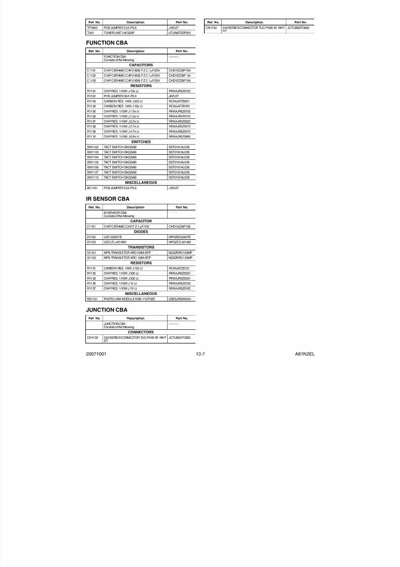
7/21/2019 Sylvania Lc195sl8 Lcd Tv Sm
http://slidepdf.com/reader/full/sylvania-lc195sl8-lcd-tv-sm 59/6020071001 13-7 A81N2EL
FUNCTION CBA
IR SENSOR CBA
JUNCTION CBA
TP1803 PCB JUMPER D0.6-P5.0 JW5.0T
TU61 TUNER UNIT U4002AF UTUNATSSP001
Ref. No. Description Part No.
FUNCTION CBAConsists of the following:
----------
CAPACITORS
C1101 CHIP CERAMIC CAP.(1608) F Z 0.1 µF/25V CHD1EZ30F104C1102 CHIP CERAMIC CAP.(1608) F Z 0.1 µF/25V CHD1EZ30F104
C1103 CHIP CERAMIC CAP.(1608) F Z 0.1 µF/25V CHD1EZ30F104
RESISTORSR1101 CHIP RES. 1/10W J 10k Ω RRXAJR5Z0103
R1102 PCB JUMPER D0.6-P5.0 JW5.0T
R1103 CARBON RES. 1/4W J 220 Ω RCX4JATZ0221R1104 CARBON RES. 1/4W J 10k Ω RCX4JATZ0103
R1105 CHIP RES. 1/10W J 1.5k Ω RRXAJR5Z0152
R1106 CHIP RES. 1/10W J 1.5k Ω RRXAJR5Z0152
R1107 CHIP RES. 1/10W J 2.2k Ω RRXAJR5Z0222
R1108 CHIP RES. 1/10W J 2.7k Ω RRXAJR5Z0272
R1109 CHIP RES. 1/10W J 4.7k Ω RRXAJR5Z0472
R1110 CHIP RES. 1/10W J 6.8k Ω RRXAJR5Z0682
SWITCHESSW1102 TACT SWITCH SKQSAB SST0101AL038
SW1103 TACT SWITCH SKQSAB SST0101AL038
SW1104 TACT SWITCH SKQSAB SST0101AL038
SW1105 TACT SWITCH SKQSAB SST0101AL038
SW1106 TACT SWITCH SKQSAB SST0101AL038
SW1107 TACT SWITCH SKQSAB SST0101AL038
SW1113 TACT SWITCH SKQSAB SST0101AL038
MISCELLANEOUSBC1101 PCB JUMPER D0.6-P5.0 JW5.0T
Ref. No. Description Part No.
IR SENSOR CBAConsists of the following:
----------
CAPACITORC1151 CHIP CERAMIC CAP. F Z 1 µF/10V CHD1AZ30F105
DIODESD1152 LED 333GT/E NPHZ00333GTE
D1153 LED LTL-4214M1 NPQZLTL4214M
TRANSISTORSQ1151 NPN TRANSISTOR KRC103M-AT/P NQSZKRC103MP
Q1152 NPN TRANSISTOR KRC103M-AT/P NQSZKRC103MP
RESISTORSR1151 CARBON RES. 1/4W J 120 Ω RCX4JATZ0121
R1152 CHIP RES. 1/10W J 330 Ω RRXAJR5Z0331
R1153 CHIP RES. 1/10W J 330 Ω RRXAJR5Z0331R1156 CHIP RES. 1/10W J 1k Ω RRXAJR5Z0102
R1157 CHIP RES. 1/10W J 10 Ω RRXAJR5Z0100
MISCELLANEOUSRS1151 PHOTO LINK MODULE KSM-712TH2E USESJRSKK044
Ref. No. Description Part No.
JUNCTION CBAConsists of the following:
----------
CONNECTORSCN1102 242 SERIES CONNECTOR TUC-P04X-B1 WHT
STJCTUB04TG002
Ref. No. Description Part No.
CN1152 242 SERIES CONNECTOR TUC-P06X-B1 WHTST
JCTUB06TG002
Ref. No. Description Part No.
7/21/2019 Sylvania Lc195sl8 Lcd Tv Sm
http://slidepdf.com/reader/full/sylvania-lc195sl8-lcd-tv-sm 60/60
© 2007 Funai Electric Co., Ltd.
All rights reserved. No part of this manual may be reproduced, copied, transmitted, disseminated, transcribed,downloaded or stored in any storage medium, in any form or for any purpose without the express prior writtenconsent of Funai. Furthermore, any unauthorized commercial distribution of this manual or any revision heretois strictly prohibited.
Information in this document is subject to change without notice. Funai reserves the right to change the contentherein without the obligation to notify any person or organization of such changes.
with the design is a registered trademark of Funai Electric Co., Ltd and may not be used in any way