switching algebra and combinational logic y
TRANSCRIPT

• •
• •
• •
• •
• •
• •
• •
• •
• •
• •
• •
• •
• •
• •
• •
• •
• •
• •
• •
• •
• •
• •
• •
• •
• •
• •
• •
• •
• •
• •
• •
• •
• •
• •
• •
• •
89
c h a p t e r 3Switching Algebra and Combinational Logic
ou have undoubtedly already used various logic expressions whenforming conditional statements in a programming language.There, variables and relations are combined in a somewhat ad-hocmanner in parenthesized expressions to make decisions and tocontrol actions.
Digital logic design employs logic expressions that are often muchmore complex than those found in a typical program. Moreover, in logicdesign such expressions usually lead to a corresponding hardware imple-mentation, a logic circuit whose output is the value obtained by evaluatingand combining the inputs as specified by the expression.
Logic expressions are therefore often manipulated—by a human ormore typically nowadays by an EDA tool—to achieve various circuit-designgoals. Such goals may include adapting an expression to an available circuitstructure or optimizing a circuit’s size or its performance in metrics likespeed and power consumption. To create, understand, and manipulate logicexpressions and circuits, digital hardware designers use switching algebraas a fundamental tool.
Logic circuits are classified into two types, “combinational” and“sequential.” A combinational logic circuit is one whose outputs dependonly on its current inputs. The fan-speed selection knob in an older car is likea combinational circuit. Its “output” selects a speed based only on its current“input”—the position of the knob.
Y
DDPP5.book Page 89 Tuesday, March 28, 2017 5:33 PM

90 Chapter 3 Switching Algebra and Combinational Logic
The outputs of a sequential logic circuit depend not only on the currentinputs but also on the past sequence of inputs, possibly arbitrarily far back intime. The fan-speed circuit controlled by up and down buttons in a newer car is asequential circuit—the current speed depends on an arbitrarily long sequence ofup/down pushes, beginning when you first turned on the fan.
This chapter focuses on combinational logic circuits, exploring switchingalgebra, logic expressions, and the analysis and synthesis of combinational logiccircuits at the gate level. Sequential circuits will be discussed in later chapters.
A combinational circuit may contain an arbitrary number of logic gatesand inverters but no feedback loops. A feedback loop is a signal path of a circuitthat allows the output of a gate to propagate back to the input of that same gate.Such a loop generally creates memory and results in sequential circuit behavior,as we’ll show in the later chapters.
In combinational circuit analysis, we start with a gate-level logic diagramand proceed to a formal description of the function performed by that circuit,like a truth table or a logic expression. In synthesis, we do the reverse, startingwith a formal description and proceeding to a logic diagram or other descriptionthat will allow us to build the circuit using available components.
Combinational circuits may have one or more outputs. In this chapter,we’ll discuss methods that apply to single-output circuits. Most analysis andsynthesis techniques can be extended in an obvious way from single-output tomultiple-output circuits (e.g., “Repeat these steps for each output”). Sometechniques can be extended to improve effectiveness for multiple outputs.
The purpose of this chapter is to give you a solid theoretical foundation forthe analysis and synthesis of combinational logic circuits, a foundation that willbe doubly important later when we move on to sequential circuits. Althoughmost analysis and synthesis procedures are automated nowadays by EDA tools,a basic understanding of the fundamentals can help you use the tools as well asunderstand what’s gone wrong when they give you undesirable results.
WHAT ISSYNTHESIS?
In Chapter 1, we introduced the concept of HDL-based digital design using EDAtools. In that approach, we can write an HDL model to precisely specify a combina-tional logic function in any of a variety of ways, and then use an EDA synthesis toolto realize the function in a selected implementation technology, as we'll describe inmore detail in Section 4.3.
In the present chapter, synthesis has a narrower meaning. We again start witha precise specification of a combinational logic function, but only in the form of alogic equation, truth table, or equivalent. And we target only one implementationtechnology, a gate-level circuit that realizes the logic function. This is traditionallogic design, where minimizing the number of gates needed to perform the functionis the key goal. For most other implementation technologies, experience has proventhat’s still a good starting point for subsequent technology-specific optimization.
synthesis
feedback loop
DDPP5.book Page 90 Tuesday, March 28, 2017 5:33 PM

3.1 Switching Algebra 91
Before launching into a discussion of combinational logic circuits, we’llintroduce switching algebra, the fundamental mathematical tool for analyzingand synthesizing logic circuits of all types.
3.1 Switching AlgebraFormal analysis techniques for digital circuits have their roots in the work of anEnglish mathematician, George Boole. In 1854, he invented a two-valuedalgebraic system, now called Boolean algebra, to “give expression … to thefundamental laws of reasoning in the symbolic language of a Calculus.” Usingthis system, a philosopher, logician, or inhabitant of the planet Vulcan canformulate propositions that are true or false, combine them to make newpropositions, and determine the truth or falsehood of the new propositions. Forexample, if we agree that “People who haven’t studied this material are eitherfailures or not nerds,” and “No computer designer is a failure,” then we cananswer questions like “If you’re a nerdy computer designer, then have youalready studied this?”
Long after Boole, in 1938, Bell Labs researcher Claude E. Shannonshowed how to adapt Boolean algebra to analyze and describe the behavior ofcircuits built from relays, the most commonly used digital logic elements of thattime. In Shannon’s switching algebra, the condition of a relay contact, open or
DESIGN VS.SYNTHESIS
Digital logic design is a superset of synthesis, since in a real design problem we startout with an informal description of the circuit’s function, typically using natural lan-guage and perhaps pseudo-code to describe its behavior. For a combinational circuit,an informal description must at least name all of the circuit’s inputs and outputs, andindicate how each output is affected by the inputs.
To formalize the circuit description, we need something that precisely definesthe circuit’s behavior for all situations; for a combinational circuit, this means theoutput values produced for all possible input combinations. Formal descriptions forcombinational circuits include truth tables, logic equations, and models created usingan HDL.
Once we have a formal circuit description, we can follow a “turn-the-crank”synthesis procedure to obtain a circuit with the specified functional behavior. Thecircuit may be described in a logic diagram that shows its elements (such as gates)and their interconnections, in a net list which is a text file conveying the same infor-mation as the latter, or in one of a myriad of formats which specify a circuit’selements and interconnections in a particular implementation technology such as anASIC or FPGA.
The material in the first three sections of this chapter is the basis for “turn-the-crank” synthesis procedures for creating combinational logic circuits using discretegates, whether the crank is turned by hand or by a computer.
Boolean algebra
switching algebra
DDPP5.book Page 91 Tuesday, March 28, 2017 5:33 PM

92 Chapter 3 Switching Algebra and Combinational Logic
closed, is represented by a variable X that can have one of two possible values,0 or 1. In today’s logic technologies, these values correspond to a wide variety ofphysical conditions—voltage HIGH or LOW, light off or on, capacitor dischargedor charged, electrons trapped or released, and so on.
In the remainder of this section, we will develop switching algebra directly,using “first principles” and what you may already know about the behavior oflogic elements (gates and inverters). For more historical and/or mathematicaltreatments of this material, consult the References section of this chapter.
3.1.1 AxiomsIn switching algebra we use a symbolic variable, such as X, to represent thecondition of a logic signal. A logic signal is in one of two possible conditions—low or high, off or on, and so on, depending on the technology. We say that Xhas the value “0” for one of these conditions and “1” for the other.
For example, with CMOS and most other logic circuits the positive-logicconvention dictates that we associate the value “0” with a LOW voltage and “1”with a HIGH voltage. The negative-logic convention, which is rarely used, makesthe opposite association: 0 = HIGH and 1 = LOW. However, the choice of positiveor negative logic has no effect on our ability to develop a consistent algebraicdescription of circuit behavior; it only affects details of the physical-to-algebraicabstraction. Thus, we may generally ignore the physical realities of logic circuitsand pretend that they operate directly on the logic symbols 0 and 1.
The axioms (or postulates) of a mathematical system are a minimal set ofbasic definitions that we assume to be true, from which all other informationabout the system can be derived. The first two axioms of switching algebraembody the “digital abstraction” by formally stating that a variable X can take ononly one of two values:
Notice that we stated these axioms as a pair, the only difference between A1 andA1D being the interchange of the symbols 0 and 1. This is a characteristic of allthe axioms of switching algebra and is the basis of the “duality” principle thatwe’ll study later.
An inverter is a logic circuit whose output signal level is the opposite (orcomplement) of its input signal level. We use a prime ( ) to denote an inverter’sfunction. That is, if a variable X denotes an inverter’s input signal, then Xdenotes the value of a signal on the inverter’s output. This notation is formallyspecified in the second pair of axioms:
Figure 3-1 shows the logic symbol for an inverter. with its input on the leftand its output on the right. The input and output signals may have arbitrarynames, say X and Y. Algebraically, however, we write Y = X to say “signal Y has
(A1) X = 0 if X ≠ 1 (A1D) X = 1 if X ≠ 0
(A2) If X = 0, then X = 1 (A2D) If X = 1, then X = 0
positive-logic convention
negative-logic convention
axiompostulate
invertercomplementprime ( )
DDPP5.book Page 92 Tuesday, March 28, 2017 5:33 PM

3.1 Switching Algebra 93
the opposite value as signal X.” The prime ( ) is an algebraic operator, and X isan expression, which you can read as “X prime” or “NOT X.” This usage is anal-ogous to what you’ve learned in programming languages, where if J is an integervariable, then −J is an expression whose value is 0 − J. Although this may seemlike a small point, you’ll learn that the distinction between signal names (X, Y),expressions (X ), and equations (Y = X ) is very important when we study docu-mentation standards and software tools for logic design. In the logic diagrams inthis book, we maintain this distinction by writing signal names in black andexpressions in color.
A 2-input AND gate is a circuit whose output is 1 if both of its inputs are 1,and it has the symbol in Figure 3-2(a). The function of a 2-input AND gate issometimes called logical multiplication and is symbolized algebraically by amultiplication dot ( ). That is, an AND gate with inputs X and Y has an output sig-nal whose value is X ⋅ Y, as shown in Figure 3-2(a). Some authors, especiallymathematicians and logicians, denote logical multiplication with a wedge(X ∧ Y). We follow standard engineering practice here by using the dot (X ⋅ Y).Verilog uses an ampersand (&) to denote the same thing.
A 2-input OR gate is a circuit whose output is 1 if either of its inputs is 1and has the symbol in Figure 3-2(b). The function of a 2-input OR gate is some-times called logical addition and is symbolized algebraically by a plus sign (+).An OR gate with inputs X and Y has an output signal whose value is X + Y, asshown in the figure. Some authors denote logical addition with a vee (X ∨ Y), butwe follow the typical engineering practice of using the plus sign (X + Y). Onceagain, other notations are used in HDLs, like “|” in Verilog.
X Y = X′Figure 3-1Signal naming and algebraic notation for an inverter.
algebraic operatorexpressionNOT operation
Figure 3-2 Signal naming and algebraic notation: (a) AND gate; (b) OR gate.
X
YZ = X · Y
X
YZ = X + Y
(a) (b)
logical multiplication
NOTE ONNOTATION
The notations X, ~X, and ¬X are also used by some authors to denote the complementof X. The overbar notation (X) is probably the most widely used and the best lookingtypographically. However, we use the prime notation to get you used to writing logicexpressions on a single text line without the more graphical overbar, and to force youto parenthesize complex complemented subexpressions—because that’s what you’llhave to do when you use HDLs like Verilog and other tools.
multiplication dot ( )
logical addition
DDPP5.book Page 93 Tuesday, March 28, 2017 5:33 PM

94 Chapter 3 Switching Algebra and Combinational Logic
By convention in this and most texts, as well as by definition in Verilog,multiplication has a higher precedence than addition in logical expressions, justas in arithmetic expressions in conventional programming languages. That is,the expression W ⋅ X + Y ⋅ Z is equivalent to (W ⋅ X) + (Y ⋅ Z). But be careful ifyou ever use VHDL. There, “and” and “or” have the same precedence and areevaluated from left to right. So, “W and X or Y and Z” has the same meaning as“((W and X) or Y) and Z”, not “(W and X) or (Y and Z)”.
The last three pairs of axioms state the formal definitions of the AND andOR operations by listing the output produced by each gate for each possibleinput combination:
The five pairs of axioms, A1–A5 and A1D–A5D, completely define switchingalgebra. All other facts about the system can be proved using these axioms as astarting point.
3.1.2 Single-Variable TheoremsDuring the analysis or synthesis of logic circuits, we can write algebraic expres-sions that characterize a circuit’s actual or desired behavior. Switching-algebratheorems are statements, known to be always true, that allow us to manipulatealgebraic expressions for simpler analysis or more efficient synthesis of thecorresponding circuits. For example, the theorem X + 0 = X allows us to substi-tute every occurrence of X + 0 in an expression with X.
Table 3-1 lists switching-algebra theorems involving a single variable X.How do we know that these theorems are true? We can either prove themourselves or take the word of someone who has. OK, we’re in college now, let’slearn how to prove them.
Most theorems in switching algebra are exceedingly simple to prove usinga technique called perfect induction. Axiom A1 is the key to this technique—
(A3) 0 ⋅ 0 = 0 (A3D) 1 + 1 = 1
(A4) 1 ⋅ 1 = 1 (A4D) 0 + 0 = 0
(A5) 0 ⋅ 1 = 1 ⋅ 0 = 0 (A5D) 1 + 0 = 0 + 1 = 1
precedence
JUXT A MINUTE… Older texts use simple juxtaposition (XY) to denote logical multiplication, but wedon’t. In general, juxtaposition is a clear notation only when signal names are limitedto a single character. Otherwise, is XY a logical product or a two-character signalname? One-character variable names are common in algebra, but in real digitaldesign problems we prefer to use multicharacter signal names that mean something.Thus, we need a separator between names, and the separator might just as well be amultiplication dot rather than a space. The HDL equivalent of the multiplication dot(like “&” in Verilog) is absolutely required when logic formulas are written in ahardware description language.
AND operationOR operation
theorem
perfect induction
DDPP5.book Page 94 Tuesday, March 28, 2017 5:33 PM

3.1 Switching Algebra 95
since a switching variable can take on only two different values, 0 and 1, we canprove a theorem involving a single variable X by proving that it is true for bothX = 0 and X = 1. For example, to prove theorem T1, we make two substitutions:
All of the theorems in Table 3-1 can be proved using perfect induction, as you’reasked to do in Drills 3.2 and 3.3.
3.1.3 Two- and Three-Variable TheoremsSwitching-algebra theorems with two or three variables are listed in Table 3-2.Each of these theorems is easily proved by perfect induction, by evaluating thetheorem statement for the four possible combinations of X and Y, or the eightpossible combinations of X, Y, and Z.
The first two theorem pairs concern commutativity and associativity oflogical addition and multiplication and are identical to the commutative andassociative laws you already know for addition and multiplication of integer andreal numbers. Taken together, they indicate that the parenthesization or order ofterms in a logical sum or logical product is irrelevant. For example, from a strict-ly algebraic point of view, an expression such as W ⋅ X ⋅ Y ⋅ Z is ambiguous; itshould be written as (W ⋅ (X ⋅ (Y ⋅ Z))) or (((W ⋅ X) ⋅ Y) ⋅ Z) or (W ⋅ X) ⋅ (Y ⋅ Z)(see Exercise 3.22). But the theorems tell us that the ambiguous form of theexpression is OK because we get the same results in any case. We even could
[X = 0] 0 + 0 = 0 true, according to axiom A4D
[X = 1] 1 + 0 = 1 true, according to axiom A5D
(T1) X + 0 = X (T1D) X 1 = X (Identities)Table 3-1Switching-algebra theorems with one variable.
(T2) X + 1 = 1 (T2D) X 0 = 0 (Null elements)
(T3) X + X = X (T3D X X = X (Idempotency)
(T4) (X ) = X (Involution)
(T5) X + X = 1 (T5 D) X ⋅ X = 0 (Complements)
Table 3-2 Switching-algebra theorems with two or three variables.
(T6) X + Y = Y + X (T6D) X ⋅ Y = Y ⋅ X (Commutativity)
(T7) (X + Y) + Z = X + (Y + Z) (T7D) (X ⋅ Y) ⋅ Z = X ⋅ (Y ⋅ Z) (Associativity)
(T8) X ⋅ Y + X ⋅ Z = X ⋅ (Y + Z) (T8D) (X + Y) ⋅ (X + Z) = X + Y ⋅ Z (Distributivity)
(T9) X + X ⋅ Y = X (T9D) X ⋅ (X + Y) = X (Covering)
(T10) X ⋅ Y + X ⋅ Y = X (T10D) (X + Y) ⋅ (X + Y ) = X (Combining)
(T11) X ⋅ Y + X ⋅ Z + Y ⋅ Z = X ⋅ Y + X′ ⋅ Z (Consensus)
(T11′) (X + Y) ⋅ (X + Z) ⋅ (Y + Z) = (X + Y) ⋅ (X + Z)
DDPP5.book Page 95 Tuesday, March 28, 2017 5:33 PM

96 Chapter 3 Switching Algebra and Combinational Logic
have rearranged the order of the variables (e.g., X ⋅ Z ⋅ Y ⋅ W) and gotten thesame results.
As trivial as this discussion may seem, it is very important, because itforms the mathematical basis for using logic gates with more than two inputs.We defined ⋅ and + as binary operators—operators that combine two variables.Yet we use 3-input and larger AND and OR gates in practice. The theorems tell uswe can connect gate inputs in any order; in fact, printed-circuit-board and ASIClayout programs take advantage of this principle to optimize wiring. Also, wecan use either one n-input gate or (n −1) 2-input gates interchangeably, thoughcost and timing delay are likely to be higher with multiple 2 input gates.
Theorem T8 is identical to the distributive law for integers and reals—thatis, logical multiplication distributes over logical addition. As a result, we can“multiply out” an expression to convert it to a sum-of-products form, as in theexample below:
V ⋅ (W + X) ⋅ (Y + Z) = V ⋅ W ⋅ Y + V ⋅ W ⋅ Z + V ⋅ X ⋅ Y + V ⋅ X ⋅ Z
However, switching algebra also has the unfamiliar property that the reverse istrue—logical addition distributes over logical multiplication—as demonstratedby theorem T8D. Thus, we can also “add out” an expression to obtain a product-of-sums form:
(V ⋅ W ⋅ X) + (Y ⋅ Z) = (V + Y) ⋅ (V + Z) ⋅ (W + Y) ⋅ (W + Z) ⋅ (X + Y) ⋅ (X + Z)
Theorems T9 and T10 are used extensively to minimize the number ofterms in logic expressions, which minimizes the number of gates or gate inputsin the corresponding logic circuits. For example, if the subexpression X + X ⋅ Yappears in a logic expression, the covering theorem T9 says that we need onlyinclude X in the expression; X is said to cover X ⋅ Y. The combining theorem T10says if the subexpression X ⋅ Y + X ⋅ Y′ appears in an expression, we can replaceit with X. Since Y must be 0 or 1, either way the original subexpression is 1 if andonly if X is 1.
Although we could easily prove T9 by perfect induction, the truth of T9may be more obvious if we prove it using the other theorems that we’ve provedso far:
Likewise, the other theorems can be used to prove T10, where the key step is touse T8 to rewrite the lefthand side as X ⋅ (Y + Y′).
Theorem T11 is known as the consensus theorem. The Y ⋅ Z term is calledthe consensus of X ⋅ Y and X′ ⋅ Z. The idea is that if Y ⋅ Z is 1, then either X ⋅ Y orX′ ⋅ Z must also be 1, since Y and Z are both 1 and either X or X′ must be 1. Thus,the Y ⋅ Z term is redundant and may be dropped from the righthand side of T11.
X + X ⋅ Y = X ⋅ 1 + X ⋅ Y (according to T1D)
= X ⋅ (1 + Y) (according to T8)
= X ⋅ 1 (according to T2)
= X (according to T1D)
binary operator
covering theoremcovercombining theorem
consensus theoremconsensus
DDPP5.book Page 96 Tuesday, March 28, 2017 5:33 PM

3.1 Switching Algebra 97
The consensus theorem has two important applications. It can be used toeliminate certain timing hazards in combinational logic circuits, as we’ll see inSection 3.4. And it also forms the basis of the iterative-consensus method usedin logic-minimization programs to find “prime implicants” (see References).
In all of the theorems, it is possible to replace each variable with anarbitrary logic expression. A simple replacement is to complement one or morevariables:
But more complex expressions may be substituted as well:
3.1.4 n-Variable TheoremsSeveral important theorems, listed in Table 3-3, are true for an arbitrary numberof variables, n. Most of these theorems can be proved using a two-step methodcalled finite induction—first proving that the theorem is true for n = 2 (the basisstep), and then proving that if the theorem is true for n = i, then it is also true forn = i + 1 (the induction step). For example, consider the generalized idempotencytheorem T12. For n = 2, T12 is equivalent to T3 and is therefore true. If it is truefor a logical sum of i X’s, then it is also true for a sum of i + 1 X’s, according tothe following reasoning:
Thus, the theorem is true for all finite values of n. DeMorgan’s theorems (T13 and T13D) are probably the most commonly
used of all the theorems of switching algebra. Theorem T13 says that an n-inputAND gate whose output is complemented is equivalent to an n-input OR gatewhose inputs are complemented. That is, the circuits of Figure 3-3(a) and (b) areequivalent.
(X + Y ) + Z X + (Y + Z ) (based on T7)
(V X) ⋅ (W ⋅ (Y Z)) + (V X) ⋅ (W ⋅ (Y Z)) V + X (based on T10)
X + X + X + … + X = X + (X + X + … + X) (i + 1 X’s on either side)
= X + (X) (if T12 is true for n = i)
= X (according to T3)
Table 3-3 Switching-algebra theorems with n variables.
(T12)(T12D)
X + X + … + X = XX ⋅ X ⋅ … ⋅ X = X
(Generalized idempotency)
(T13)(T13D
(X1 ⋅ X2 ⋅ … ⋅ Xn) = X1 + X2 … + Xn
(X1 + X2 + … + Xn) = X1 X2 … ⋅ Xn
(DeMorgan’s theorems)
(T14) [F(X1, X2, …, Xn, +, ⋅ )] = F(X1 , X2 , …, Xn , ⋅ , +) (Generalized DeMorgan’s theorem)
(T15)(T15D)
F(X1, X2, …, Xn) = X1 ⋅ F(1, X2, …, Xn) + X1 F(0, X2, …, Xn)
F(X1, X2, …, Xn) = [X1 + F(0,X2,…,Xn)] ⋅ [X1 F(1, X2, …, Xn)]
(Shannon’s expansion theorems)
finite inductionbasis stepinduction step
DeMorgan’s theorems
DDPP5.book Page 97 Tuesday, March 28, 2017 5:33 PM

98 Chapter 3 Switching Algebra and Combinational Logic
A NAND gate is like an AND gate, but with its output complemented, andthus can have the logic symbol in Figure 3-3(c). However, a typical CMOSNAND-gate circuit typically is not designed at the transistor level as an AND gatefollowed by a transistor inverter (NOT gate); it’s just a collection of transistorsthat happens to perform the AND-NOT function. In fact, theorem T13 tells usthat the logic symbol in Figure 3-3(d) denotes the same logic function (bubbleson the OR-gate inputs indicate logical inversion). That is, a NAND gate may beconsidered to perform a NOT-OR function.
By observing the inputs and output of a NAND gate, it is impossible todetermine whether it has been built internally as an AND gate followed by aninverter, as inverters followed by an OR gate, or as a direct CMOS realization,because all NAND gates perform precisely the same logic function. Although thechoice of symbol has no bearing on a gate’s functionality, the proper symbolchoice in documentation for a larger circuit incorporating the gate can make thelarger circuit easier to understand, as we’ll see in later chapters.
Another symbolic equivalence can be inferred from theorem T13D. Asshown in Figure 3-4, a NOR gate may be realized as an OR gate followed by aninverter, or as inverters followed by an AND gate. Once again, the choice of oneor the other of the equivalent logic symbols can make a big difference in theunderstandability of a larger circuit.
Theorems T13 and T13D happen to be just special cases of a generalizedDeMorgan’s theorem, T14, that applies to an arbitrary logic expression F. By
X
Y
X
Y
X
Y
Z = (X · Y)′ Z = (X · Y)′
X′
Y′
X
Y
Z = X′ + Y′
(a) (c)
(b) Z = X′ + Y′(d)
X · Y
Figure 3-3 Equivalent circuits according to DeMorgan’s theorem T13: (a) AND-NOT; (b) NOT-OR; (c) logic symbol for a NAND gate; (d) equivalent symbol for a NAND gate.
X
Y
X
Y
X
Y
Z = (X + Y)′ Z = (X + Y)′
X′
Y′
X
Y
Z = X′ · Y′
(a) (c)
(b) Z = X′ · Y′(d)
X + Y
Figure 3-4 Equivalent circuits according to DeMorgan’s theorem T13D: (a) OR-NOT; (b) NOT-AND; (c) logic symbol for a NOR gate; (d) equivalent symbol for a NOR gate.
generalized DeMorgan’s theorem
DDPP5.book Page 98 Tuesday, March 28, 2017 5:33 PM

3.1 Switching Algebra 99
definition, the complement of a logic expression, written as (F)′, is an expressionwhose value is the opposite of F’s for all possible input combinations. TheoremT14 is very important because it gives us a way to manipulate and simplify thecomplement of an expression.
Theorem T14 states that, given any n-variable logic expression, its comple-ment can be obtained by swapping the + and ⋅ operators and complementing allvariables. For example, suppose that we have
In the second line, we have enclosed complemented variables in parentheses toremind you that the ′ is an operator, not part of the variable name. By applyingtheorem T14, we obtain
Using theorem T4, this can be simplified to
In general, we can use theorem T14 to complement a parenthesized expressionby swapping + and ⋅ , complementing all uncomplemented variables, anduncomplementing all complemented ones.
The generalized DeMorgan’s theorem T14 can be proved by showing thatall logic functions can be written as either a sum or a product of subfunctions,and then applying T13 and T13D recursively. Also, an enlightening and satisfy-ing proof is presented in previous editions of this book, based on the principle ofduality which we explain in the next subsection.
Shannon’s expansion theorems T15 and T15D are very important for theiruse in FPGAs to implement arbitrary combinational logic functions. An FPGAcontains many instances of a basic resource called a lookup table (LUT) that canrealize any combinational logic function of up to a certain number of inputs, onthe order of 6. What if you need a 7-input function? Shannon’s theorems tell youhow to combine the outputs of two 6-input LUTs to realize any 7-input function.Similarly, 8-input functions can be implemented by combining 7-input functionsrealized this way (with 4 LUTs total), and so on. Logic synthesizers for FPGAsdo this automatically, as discussed in Section 6.1.3 on page 244.
3.1.5 DualityWe stated all of the axioms of switching algebra in pairs. The dual of each axiom(e.g., A5D) is obtained from the base axiom (e.g., A5) by simply swapping 0and 1 and, if present, ⋅ and +. As a result, we can state the following metatheorem(a metatheorem is a theorem about theorems):
Principle of Duality Any theorem or identity in switching algebra is also true if0 and 1 are swapped and ⋅ and + are swapped throughout.
F(W, X, Y, Z) = (W′ ⋅ X) + (X ⋅ Y) + (W ⋅ (X′ + Z′))= ((W)′ ⋅ X) + (X ⋅ Y) + (W ⋅ ((X)′ + (Z)′))
[F(W, X, Y, Z)]′ = ((W′)′ + X′) ⋅ (X′ + Y′) ⋅ (W′ + ((X′)′ ⋅ (Z′)′))
[F(W, X, Y, Z)]′ = (W + X′) ⋅ (X′ + Y′) ⋅ (W′ + (X ⋅ Z))
complement of a logic expression
dual
metatheorem
DDPP5.book Page 99 Tuesday, March 28, 2017 5:33 PM
100 Chapter 3 Switching Algebra and Combinational Logic
The metatheorem is true because the duals of all the axioms are true, so duals ofall switching-algebra theorems can be proved using duals of the axioms.
After all, what’s in a name, or in a symbol for that matter? If the softwarethat was used to format this book had a bug, one that swapped 0 ↔ 1 and ⋅ ↔ +throughout this chapter, you still would have learned exactly the same switchingalgebra; only the nomenclature would have been a little weird, using words like“product” to describe an operation that uses the symbol “+”.
Duality is important because it doubles the usefulness of almost everythingthat you know about switching algebra and manipulation of switching functions.This statement applies not only to you, but also to automated tools that manipu-late logic functions and synthesize circuits that perform them. For example, if asoftware tool can derive a sum-of-products expression from an arbitrarycombinational logic function defined in an HDL model, and synthesize a corre-sponding two-stage AND-OR logic circuit from that expression, then withrelatively little effort, it can be adapted also to derive a product-of-sums expres-sion and synthesize a corresponding OR-AND circuit for the same logicfunction. We explore this idea in Exercise 3.41.
There is just one convention in switching algebra where we did not treat ⋅and + identically, so duality does not necessarily hold true—can you rememberwhat it is before reading the answer below? Consider the following statement oftheorem T9 and its clearly absurd “dual”:
Obviously the last line above is false—where did we go wrong? The problem isin operator precedence. We were able to write the lefthand side of the first linewithout parentheses because of our convention that ⋅ has precedence. However,once we applied the principle of duality, we should have given precedence to +instead, or written the second line as X ⋅ (X + Y) = X. The best way to avoidproblems like this is to parenthesize an expression fully before taking its dual.
3.1.6 Standard Representations of Logic FunctionsBefore moving on to analysis and synthesis of combinational logic functions,we’ll introduce some needed nomenclature and notation.
The most basic representation of a logic function is the truth table. Similarin approach to the perfect-induction proof method, this brute-force representa-tion simply lists the output of the circuit for every possible input combination.Traditionally, the input combinations are arranged in rows in ascending binarycounting order, and the corresponding output values are written in a column nextto the rows. For example, the general structure of a 3-variable truth table is
X + X ⋅ Y = X (theorem T9)
X ⋅ X + Y = X (after applying the principle of duality)
X + Y = X (after applying theorem T3D)
truth table
DDPP5.book Page 100 Tuesday, March 28, 2017 5:33 PM

3.1 Switching Algebra 101
shown in Table 3-4. The rows of the table are numbered 0–7, corresponding tothe binary input combinations, but this numbering is not a necessary part of thetruth table.
The truth table for a particular 3-variable logic function is shown inTable 3-5. Each distinct pattern of eight 0s and 1s in the output column yields adifferent logic function; there are 28 such patterns. Thus, the logic function inTable 3-5 is one of 28 different logic functions of three variables.
The truth table for an n-variable logic function has 2n rows. Obviously,truth tables are practical to write only for logic functions with a small number ofvariables, say, 10 for students and about 4–5 for everyone else.
The information contained in a truth table can also be conveyed algebra-ically. To do so, we first need some definitions:
• A literal is a variable or the complement of a variable. Examples: X, Y, X′,Y′.
• A product term is a single literal or a logical product of two or moreliterals. Examples: Z′, W ⋅ X ⋅ Y, X ⋅ Y′ ⋅ Z, W′ ⋅ Y′ ⋅ Z.
Row X Y Z F
Table 3-4General truth table structure for a 3-variable logic function, F(X,Y, Z).
0 0 0 0 F(0,0,0)
1 0 0 1 F(0,0,1)
2 0 1 0 F(0,1,0)
3 0 1 1 F(0,1,1)
4 1 0 0 F(1,0,0)
5 1 0 1 F(1,0,1)
6 1 1 0 F(1,1,0)
7 1 1 1 F(1,1,1)
Row X Y Z F
Table 3-5Truth table for a particular 3-variable logic function, F(X,Y, Z).
0 0 0 0 1
1 0 0 1 0
2 0 1 0 0
3 0 1 1 1
4 1 0 0 1
5 1 0 1 0
6 1 1 0 1
7 1 1 1 1
literal
product term
DDPP5.book Page 101 Tuesday, March 28, 2017 5:33 PM
102 Chapter 3 Switching Algebra and Combinational Logic
• A sum-of-products expression is a logical sum of product terms. Example:Z + W ⋅ X ⋅ Y + X ⋅ Y Z + W Y Z.
• A sum term is a single literal or a logical sum of two or more literals.Examples: Z , W + X + Y, X + Y Z, W Y Z.
• A product-of-sums expression is a logical product of sum terms. Example:Z ⋅ (W + X + Y) ⋅ (X + Y Z) ⋅ (W Y Z).
• A normal term is a product or sum term in which no variable appears morethan once. A nonnormal term can always be simplified to a constant or anormal term using one of theorems T3, T3 , T5, or T5 . Examples of non-normal terms: W ⋅ X ⋅ X ⋅ Y , W + W + X + Y, X ⋅ X Y. Examples ofnormal terms: W ⋅ X ⋅ Y , W + X Y.
• An n-variable minterm is a normal product term with n literals. Thereare 2n such product terms. Some examples of 4-variable minterms:W′ ⋅ X Y Z , W ⋅ X ⋅ Y Z, W X Y ⋅ Z .
• An n-variable maxterm is a normal sum term with n literals. There are 2n
such sum terms. Examples of 4-variable maxterms: W + X + Y + Z ,W + X + Y + Z, W + X + Y + Z .
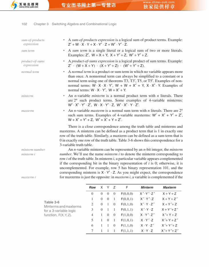
There is a close correspondence among the truth table and minterms andmaxterms. A minterm can be defined as a product term that is 1 in exactly onerow of the truth table. Similarly, a maxterm can be defined as a sum term that is0 in exactly one row of the truth table. Table 3-6 shows this correspondence for a3-variable truth table.
An n-variable minterm can be represented by an n-bit integer, the mintermnumber. We’ll use the name minterm i to denote the minterm corresponding torow i of the truth table. In minterm i, a particular variable appears complementedif the corresponding bit in the binary representation of i is 0; otherwise, it isuncomplemented. For example, row 5 has binary representation 101, and thecorresponding minterm is X ⋅ Y Z. As you might expect, the correspondencefor maxterms is just the opposite: in maxterm i, a variable is complemented if the
sum-of-products expression
sum term
product-of-sums expression
normal term
minterm
maxterm
Table 3-6Minterms and maxterms for a 3-variable logic function, F(X,Y, Z).
Row X Y Z F Minterm Maxterm
minterm numberminterm i
maxterm i
DDPP5.book Page 102 Tuesday, March 28, 2017 5:33 PM

3.1 Switching Algebra 103
corresponding bit in the binary representation of i is 1. Thus, maxterm 5 (101)is X′ + Y + Z′. Note that all of this makes sense only if we have stated the numberof variables, three in the examples.
Based on the correspondence between the truth table and minterms, we caneasily create an algebraic representation of a logic function from its truth table.The canonical sum of a logic function is a sum of the minterms corresponding totruth-table rows (input combinations) for which the function produces a 1output. For example, the canonical sum for the logic function in Table 3-5 onpage 101 is
Here, the notation ΣX,Y,Z(0, 3, 4, 6, 7) is a minterm list and means “the sum ofminterms 0, 3, 4, 6, and 7 with variables X, Y, and Z.” The minterm list is alsoknown as the on-set for the logic function. You can visualize that each minterm“turns on” the output for exactly one input combination. Any logic function canbe written as a canonical sum.
The canonical product of a logic function is a product of the maxtermscorresponding to input combinations for which the function produces a 0 output.For example, the canonical product for the logic function in Table 3-5 is
Here, the notation ∏X,Y,Z(1, 2, 5) is a maxterm list and means “the product ofmaxterms 1, 2, and 5 with variables X, Y, and Z.” The maxterm list is also knownas the off-set for the logic function. You can visualize that each maxterm “turnsoff” the output for exactly one input combination. Any logic function can bewritten as a canonical product.
It’s easy to convert between a minterm list and a maxterm list. For afunction of n variables, the possible minterm and maxterm numbers are in the set{0, 1, … , 2n − 1}; a minterm or maxterm list contains a subset of these numbers.To switch between list types, take the set complement, for example:
A combinational logic function can also be described in many differentways by statements in an HDL. In Verilog, a case statement can be written thatcorresponds directly to the minterm list or maxterm list of a function. For theexample logic function that we’ve been using, from Table 3-5 on page 101, wecould write the following Verilog statement corresponding to the minterm list:
F = ΣX,Y,Z(0, 3, 4, 6, 7)
= X′ ⋅ Y′ ⋅ Z′ + X′ ⋅ Y ⋅ Z + X ⋅ Y′ ⋅ Z′ + X ⋅ Y ⋅ Z′ + X ⋅ Y ⋅ Z
F = ∏X,Y,Z(1, 2, 5)
= (X + Y + Z′) ⋅ (X + Y′ + Z) ⋅ (X′ + Y + Z′)
ΣA,B,C(0,1,2,3) = ∏A,B,C(4,5,6,7)
ΣX,Y(1) = ∏X,Y(0,2,3)
ΣW,X,Y,Z(0,1,2,3,5,7,11,13) = ∏W,X,Y,Z(4,6,8,9,10,12,14,15)
canonical sum
minterm list
on-set
canonical product
maxterm list
off-set
DDPP5.book Page 103 Tuesday, March 28, 2017 5:33 PM

104 Chapter 3 Switching Algebra and Combinational Logic
case ({X,Y,Z}) 0,3,4,6,7: F = 1; default: F = 0;endcase
Here, the braces {} convert the three 1-bit inputs into a 3-bit value used to selecta case; the minterm numbers are listed for the cases where the function’s valueis 1; and the default value for unlisted cases is specified to be 0. We could alsowrite Verilog for the corresponding maxterm list as follows:
case ({X,Y,Z}) 1,2,5: F = 0; default: F = 1;endcase
The Verilog statements above are of course just code fragments, but we’ll givedetails of the language in Chapter 5.
We have now learned six equivalent representations for a combinationallogic function:
1. A truth table.
2. An algebraic sum of minterms, the canonical sum.
3. A minterm list using the Σ notation.
4. An algebraic product of maxterms, the canonical product.
5. A maxterm list using the Π notation.
6. A Verilog case statement.
Each one of these representations specifies exactly the same information; givenany one of them, we can derive any of the others using a simple process of selec-tion and/or substitution. For example, to go from a minterm list to a canonicalproduct, we create a truth table with a 1 in each row corresponding to a listedminterm number, and then write the algebraic product of the maxterms corre-sponding to each truth-table row that does not have a 1 in it.
3.2 Combinational-Circuit AnalysisWe can analyze a combinational logic circuit by obtaining a formal descriptionof its logic function. Once we have a description of the logic function, we canperform a number of other operations:
• Determine the behavior of the logic circuit for various input combinations.We can do this with paper and pencil, or use an EDA tool—a simulator.
• Manipulate an algebraic or equivalent graphical description to suggest dif-ferent circuit elements or structures for the logic function. Some suchmanipulations are very straightforward and may make the circuit’s func-tion easier to understand.
DDPP5.book Page 104 Tuesday, March 28, 2017 5:33 PM

3.2 Combinational-Circuit Analysis 105
• Transform an algebraic description into a standard form corresponding toan available circuit structure; such an operation could be used by a soft-ware tool to “realize” (make real) a circuit that performs the logic function.For example, a truth table corresponds to the function “lookup-table”(LUT) memory used in FPGAs (field programmable gate arrays), and asum-of-products expression corresponds directly to the circuit structureused in PLDs (programmable logic devices).
• Use an algebraic description of the circuit’s functional behavior in the anal-ysis of a larger system that contains the circuit.
In this subsection we’ll focus on operations that you can carry out by hand forsmall circuits, but we’ll also point out how equivalent operations can be done bylogic-design software tools.
Given a logic diagram for a combinational circuit, like Figure 3-5, there areseveral ways to obtain a formal description of the circuit’s function. The mostbasic functional description is the truth table.
Using only the basic axioms of switching algebra, we can obtain the truthtable of an n-input circuit by working our way through all 2n input combinations.For each input combination, we determine all of the gate outputs produced bythat input, propagating information from the circuit inputs to the circuit outputs.Figure 3-6 applies this “exhaustive” technique to our example circuit. Writtenon each signal line in the circuit is a sequence of eight logic values, the values
Figure 3-5A 3-input,1-output logic circuit.
F
X
Y
Z
YN
XN
ZN
XYN
XYNZ
XNYZN
01100101
01000101
00100000
11001111
01010101
11110000
01010101
00110011 11001100
00110011
10101010
0000111100001111
F
X
Y
ZYN
XN
ZN
XYN
XYNZ
XNYZN
Figure 3-6 Gate outputs created by all input combinations.
DDPP5.book Page 105 Tuesday, March 28, 2017 5:33 PM

106 Chapter 3 Switching Algebra and Combinational Logic
present on that line when the circuit inputs X Y Z are 000, 001, …, 111. Theoutput column F of the truth table can be filled in by transcribing the outputsequence of the final OR gate, as shown in Table 3-7. Once we have the truthtable for the circuit, we can also directly write a logic expression—the canonicalsum or product—for F if we wish.
Table 3-7Truth table for the logic circuit of Figure 3-5.
Row X Y Z F
0 0 0 0 0
1 0 0 1 1
2 0 1 0 1
3 0 1 1 0
4 1 0 0 0
5 1 0 1 1
6 1 1 0 0
7 1 1 1 1
Figure 3-7 Simulator timing diagram for logic circuit.
A LESSEXHAUSTING
WAY TO GO
You can easily obtain the results in Figure 3-6 with typical EDA tools that include alogic simulator. First, you draw the logic diagram or create an equivalent “structural”HDL model. Then, in the simulator, you apply 3-bit combinations to the circuit’s X,Y, and Z inputs in binary counting order as in the figure. (Many simulators havecounters built in for just this sort of exercise.) The simulator allows you to create atiming diagram of the resulting signal values at any point in the schematic, includingthe intermediate points as well as the output.
Figure 3-7 is a timing diagram produced by the simulator when a 3-bit counterwas provided to step through the input combinations, one every 10 ns. The simulatedoutput values on the signal lines correspond exactly to those shown in Figure 3-6.
DDPP5.book Page 106 Tuesday, March 28, 2017 5:33 PM

3.2 Combinational-Circuit Analysis 107
The number of input combinations of a logic circuit grows exponentiallywith the number of inputs, so the exhaustive approach can quickly becomeexhausting. For many analysis problems, it may be better to use an algebraicapproach whose complexity is more linearly proportional to the size of the cir-cuit. The method is simple—we build up a parenthesized logic expressioncorresponding to the logic operators and structure of the circuit. We start at thecircuit inputs and propagate expressions through gates toward the output. Usingthe theorems of switching algebra, we may simplify the expressions as we go, orwe may defer all algebraic manipulations until an output expression is obtained.
Figure 3-8 applies the algebraic technique to our example circuit. The out-put function is given on the output of the final OR gate:
No switching-algebra theorems were used to obtain this expression. However,we can use theorems to transform this expression into another form. Forexample, a sum of products can be obtained by “multiplying out”:
The new expression leads to a different circuit for the same logic function, asshown in Figure 3-9.
F = ((X+Y′) ⋅ Z) + (X′ ⋅ Y ⋅ Z′)
F = X ⋅ Z + Y′ ⋅ Z + X′ ⋅ Y ⋅ Z′
F
X
YY′
X + Y′
(X + Y′ ) · Z
X′
Z′
Z
= ((X + Y′) · Z) + (X′ · Y · Z′)
X′ · Y · Z′
Figure 3-8 Logic expressions for signal lines.
F = X · Z + Y′ · Z + X′ · Y · Z′
X
Y
Z
Y′Y′ · Z
X · Z
X′ · Y · Z′
X′
Z′
Figure 3-9 Two-level AND-OR circuit.
DDPP5.book Page 107 Tuesday, March 28, 2017 5:33 PM

108 Chapter 3 Switching Algebra and Combinational Logic
Similarly, we can “add out” the original expression to obtain a product ofsums corresponding to the logic circuit in Figure 3-10:
Our next example of algebraic analysis uses a circuit with NAND and NORgates, shown in Figure 3-11. This analysis is a little messier than the previousexample, because each gate produces a complemented subexpression, not just asimple sum or product. However, the output expression can be simplified byrepeated application of the generalized DeMorgan’s theorem:
F = ((X + Y′) ⋅ Z) + (X′ ⋅ Y ⋅ Z′)= (X + Y′ + X′) ⋅ (X + Y′ + Y) ⋅ (X + Y′ + Z′) ⋅ (Z + X′) ⋅ (Z + Y) ⋅ (Z + Z′)= 1 ⋅ 1 ⋅ (X + Y′ + Z′) ⋅ (X′ + Z) ⋅ (Y + Z) ⋅ 1
= (X + Y′ + Z′) ⋅ (X′ + Z) ⋅ (Y + Z)
F = [((W ⋅ X′)′ ⋅ Y)′ + (W′ + X + Y′)′ + (W + Z)′]′= ((W′ + X)′ + Y′)′ ⋅ (W ⋅ X′ ⋅ Y)′ ⋅ (W′ ⋅ Z′)′= ((W ⋅ X′)′ ⋅ Y) ⋅ (W′ + X + Y′) ⋅ (W + Z)
= ((W′ + X) ⋅ Y) ⋅ (W′ + X + Y′) ⋅ (W + Z)
X
Y
Z
Y′
Y + Z
X′ + Z
X + Y′ + Z′
X′
Z′
F = (X + Y′ + Z′) · (X′ + Z) · (Y + Z)
Figure 3-10 Two-level OR-AND circuit.
F
X
W
Y
Z
= [((W · X′)′ · Y)′ + (W′ + X + Y′)′+ (W + Z)′]′
X′(W · X′)′
((W · X′)′ · Y)′
(W′ + X + Y′)′
(W + Z)′
W′
Y′
Figure 3-11 Algebraic analysis of a logic circuit with NAND and NOR gates.
DDPP5.book Page 108 Tuesday, March 28, 2017 5:33 PM

3.2 Combinational-Circuit Analysis 109
Quite often, DeMorgan’s theorem can be applied graphically to simplifyalgebraic analysis. Recall from Figures 3-3 and 3-4 that NAND and NOR gateseach have two equivalent symbols. By judiciously redrawing Figure 3-11, wemake it possible to cancel out some of the inversions during the analysis by usingtheorem T4 [(X′)′ = X], as shown in Figure 3-12. This manipulation leads usdirectly to a simplified output expression:
Figures 3-11 and 3-12 were just two different ways of drawing the samephysical logic circuit. However, when we simplify a logic expression using thetheorems of switching algebra, we get an expression corresponding to a differentphysical circuit. For example, the simplified expression above corresponds tothe circuit of Figure 3-13, which is physically different from the one in theprevious two figures. Furthermore, we could multiply out and add out theexpression to obtain sum-of-products and product-of-sums expressions corre-sponding to two more physically different circuits for the same logic function.
F = ((W′ + X) ⋅ Y) ⋅ (W′ + X + Y′) ⋅ (W + Z)
F
X
W
Y
Z
= ((W′ + X) · Y) · (W′ + X + Y′)· (W + Z)
X′W′ + X
((W′ + X) · Y)′
(W′ + X + Y′)′
(W + Z)′
W′
Y′
Figure 3-12 Algebraic analysis of previous circuit after substituting some NAND and NOR symbols.
F
X
W
Y
Z
= ((W′ + X) · Y) · (W′ + X + Y′)· (W + Z)
X′W′ + X
(W′ + X) · Y
W′ + X + Y′
W + Z
W′
Y′
Figure 3-13 A different circuit for same logic function.
DDPP5.book Page 109 Tuesday, March 28, 2017 5:33 PM

110 Chapter 3 Switching Algebra and Combinational Logic
Although we used logic expressions above to convey information about thephysical structure of a circuit, we don’t always do this. For example, we mightuse the expression G(W, X, Y, Z) = W ⋅ X ⋅ Y + Y ⋅ Z to describe any of the circuitsin Figure 3-14. Normally, the only sure way to determine a circuit’s structure isto look at its logic diagram. However, for certain restricted classes of circuits,structural information can be inferred from logic expressions. For example, thecircuit in (a) could be described without reference to the drawing as “a two-levelAND-OR circuit for W ⋅ X ⋅ Y + Y ⋅ Z,” while the circuit in (b) could be describedas “a two-level NAND-NAND circuit for W ⋅ X ⋅ Y + Y ⋅ Z.”
3.3 Combinational-Circuit SynthesisWe may use the words “digital design” to refer broadly to an entire process, fromconcept to physical design of a digital logic circuit or system. However, we usethe word synthesis more narrowly, referring to the process that starts with aprecise formal specification of the required function and creates details of animplementation—a physical logic circuit that performs the function.
What is the starting point for the design of combinational logic circuits?Usually, we are given a word description of a problem, or we develop one our-selves. Unless we’re constrained to use a particular technology to realize thecorresponding physical circuit (as in this chapter, where we’re only looking atdiscrete gates), the next step would be to select the target technology, since dif-ferent ones may have different synthesis tools. We should develop the circuit’sformal specification in a format that is compatible with those tools.
WX
Y
Z
G
(a) (b)
(c)
WX
Y
Z
G
GW
X
Y
Z
Y′
W · X · Y
W · X · Y
(W · X · Y)′
(W · X)′
(Y · Z)′Y · Z
Y · Z
Figure 3-14 Three circuits for G(W, X, Y, Z) = W ⋅ X ⋅Y + Y ⋅ Z: (a) two-level AND-OR; (b) two-level NAND-NAND; (c) with 2-input gates only.
DDPP5.book Page 110 Tuesday, March 28, 2017 5:33 PM

3.3 Combinational-Circuit Synthesis 111
In modern digital-design environments, the word description may be con-verted into a model in a hardware description language (HDL) like Verilog, andwe’ll see many examples of that beginning in Chapter 6. In the current chapter,which targets discrete gate-level designs, we’ll look at synthesis methods thatstart with specifications using one of the tabular or algebraic representations thatwe introduced in Section 3.1.
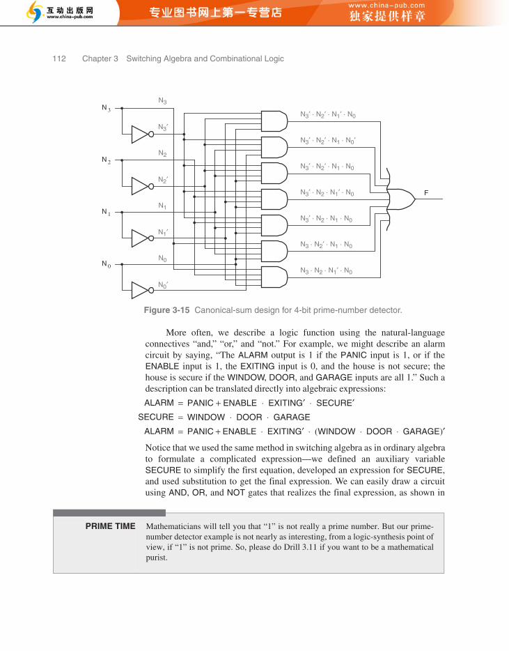
3.3.1 Circuit Descriptions and DesignsOccasionally, a logic circuit description is just a list of input combinations forwhich a signal should be on or off, the verbal equivalent of a truth table or the Σor ∏ notation introduced previously. For example, the description of a 4-bitprime-number detector might be, “Given a 4-bit input combination N =N3N2N1N0, produce a 1 output for N = 1, 2, 3, 5, 7, 11, 13, and 0 otherwise.” Alogic function described in this way can be designed directly from the canonicalsum or product expression. For the prime-number detector, we have
The corresponding circuit is shown in Figure 3-15.
F = ΣN3,N2,N1,N0(1, 2, 3, 5, 7, 11, 13)
= N3′ ⋅N2′ ⋅N1′ ⋅N0 + N3′ ⋅N2′ ⋅N1 ⋅N0′ + N3′ ⋅N2′ ⋅N1 ⋅N0+ N3′ ⋅N2 ⋅N1′ ⋅N0
+ N3′ ⋅N2 ⋅N1 ⋅N0 + N3 ⋅N2′ ⋅N1 ⋅N0 + N3 ⋅N2 ⋅N1′ ⋅N0
WHY STUDYGATE-LEVELSYNTHESIS?
Most digital design nowadays is carried out using building blocks that are larger(perhaps much larger) than discrete gates, or using HDLs and synthesizers that createthe corresponding physical implementations. There’s no need for the designer to getinvolved with synthesis at the level described in this section. To design a micro-processor with millions of gates, an HDL-based approach for the “routine” parts ofthe design is essential if the it’s ever to be completed.
However, sometimes the synthesizer’s results just aren’t good enough. Toachieve performance goals, it may still be necessary for critical blocks (such asadders, multipliers, multiplexers, and specialized high-speed control circuits) to besynthesized “by hand,” with the designer playing an active role in the selection ofgate-level structures and interconnections, and even guiding physical layout in thecase of both ASIC and FPGA design.
There are also cases where the synthesizer may “run amok,” creating a circuitthat is much less efficient (in speed, size, or some other metric) than what is expectedand required. In these cases, it is important for the designer to have a good feel forwhat could be achieved, and perhaps try a different style of HDL modeling or struc-turing to cajole the synthesizer into creating a result that is closer to what is desired.We’ll see some examples of that in Chapters 6 and 8.
A basic understanding of combinational logic synthesis at the level presentedin this section can help you develop such a “good feel.”
DDPP5.book Page 111 Tuesday, March 28, 2017 5:33 PM
112 Chapter 3 Switching Algebra and Combinational Logic
More often, we describe a logic function using the natural-languageconnectives “and,” “or,” and “not.” For example, we might describe an alarmcircuit by saying, “The ALARM output is 1 if the PANIC input is 1, or if theENABLE input is 1, the EXITING input is 0, and the house is not secure; thehouse is secure if the WINDOW, DOOR, and GARAGE inputs are all 1.” Such adescription can be translated directly into algebraic expressions:
Notice that we used the same method in switching algebra as in ordinary algebrato formulate a complicated expression—we defined an auxiliary variableSECURE to simplify the first equation, developed an expression for SECURE,and used substitution to get the final expression. We can easily draw a circuitusing AND, OR, and NOT gates that realizes the final expression, as shown in
ALARM = PANIC + ENABLE ⋅ EXITING′ ⋅ SECURE′SECURE = WINDOW ⋅ DOOR ⋅ GARAGE
ALARM = PANIC + ENABLE ⋅ EXITING′ ⋅ (WINDOW ⋅ DOOR ⋅ GARAGE)′
N 3
N3
N3′
N3′ · N2′ · N1′ · N0
N3′ · N2′ · N1 · N0′
N3′ · N2′ · N1 · N0
N3′ · N2 · N1′ · N0
N3′ · N2 · N1 · N0
N3 · N2′ · N1 · N0
N3 · N2 · N1′ · N0
N2
N2′
N1
N1′
N0
N0′
N 2
N 1
N 0
F
Figure 3-15 Canonical-sum design for 4-bit prime-number detector.
PRIME TIME Mathematicians will tell you that “1” is not really a prime number. But our prime-number detector example is not nearly as interesting, from a logic-synthesis point ofview, if “1” is not prime. So, please do Drill 3.11 if you want to be a mathematicalpurist.
DDPP5.book Page 112 Tuesday, March 28, 2017 5:33 PM

3.3 Combinational-Circuit Synthesis 113
Figure 3-16. A circuit realizes (“makes real”) an expression if its output functionequals that expression, and the circuit is called a realization of the function. Wecan and will also call it an implementation; both terms are used in practice.
Once we have an expression, any expression, for a logic function, we cando other things besides building a circuit directly from the expression. We canmanipulate the expression to get different circuits. For example, the ALARMexpression above can be multiplied out to get the sum-of-products circuit inFigure 3-17. Or, if the number of variables is not too large, we can construct thetruth table for the expression and use any of the synthesis methods that apply totruth tables, including the canonical sum or product method described earlierand the minimization methods to be described later.
In general, when we’re designing a logic function for an application, it’seasier to describe it in words using logical connectives and to write the corre-sponding logic expressions than it is to write a complete truth table, especially ifthe number of variables is large. However, sometimes we start with impreciseword descriptions of logic functions, for example, “The ERROR output shouldbe 1 if the GEARUP, GEARDOWN, and GEARCHECK inputs are inconsistent.”In this situation, the truth-table approach is best because it allows us to deter-mine the output required for every input combination, based on our knowledgeand understanding of the problem environment (e.g., the brakes cannot beapplied unless the gear is down). Using a logic expression may make it difficultto notice so-called “corner cases” and handle them appropriately.
PANICALARM
ENABLE
EXITING
WINDOW
DOOR
GARAGE
SECURE
Figure 3-16 Alarm circuit derived from logic expression.
realizerealizationimplementation
PANIC
ALARM
ENABLE
EXITING
WINDOW
DOOR
GARAGE
= PANIC+ ENABLE · EXITING′ · WINDOW′ + ENABLE · EXITING′ · DOOR′ + ENABLE · EXITING′ · GARAGE′
Figure 3-17 Sum-of-products version of alarm circuit.
DDPP5.book Page 113 Tuesday, March 28, 2017 5:33 PM

114 Chapter 3 Switching Algebra and Combinational Logic
3.3.2 Circuit ManipulationsThe design methods that we’ve described so far use AND, OR, and NOT gates.We might like to use NAND and NOR gates, too—they’re faster than ANDs andORs in most technologies, including typical CMOS ASIC libraries. However,most people don’t develop logical propositions in terms of NAND and NOR con-nectives. That is, you probably wouldn’t say, “I won’t date you if you’re notclean or not wealthy and also you’re not smart or not friendly.” It would be morenatural for you to say, “I’ll date you if you’re clean and wealthy, or if you’resmart and friendly.” So, given a “natural” logic expression, we need ways totranslate it into other forms for efficient implementation.
We can translate any logic expression into an equivalent sum-of-productsexpression, simply by multiplying it out. As shown in Figure 3-18(a), a sum-of-products expression can be realized directly with AND and OR gates. The invert-ers needed for complemented inputs are not shown.
Figure 3-18Alternative sum-of-products circuits: (a) AND-OR; (b) AND-OR with extra inverter pairs; (c) NAND-NAND.
(c)
(a)
(b)
DDPP5.book Page 114 Tuesday, March 28, 2017 5:33 PM

3.3 Combinational-Circuit Synthesis 115
As shown in Figure 3-18(b), we can insert a pair of inverters between eachAND-gate output and the corresponding OR-gate input in a two-level AND-ORcircuit. According to theorem T4, these inverters have no effect on the outputfunction of the circuit. In fact, we’ve drawn the second inverter of each pairwith its inversion bubble on its input to provide a graphical reminder that theinverters cancel. However, if these inverters are absorbed into the AND and ORgates, we wind up with AND-NOT gates at the first level and a NOT-OR gateat the second level. These are just two different symbols for the same type ofgate—a NAND gate. Thus, a two-level AND-OR circuit may be converted to atwo-level NAND-NAND circuit simply by substituting gates.
If any product terms in the sum-of-products expression contain just oneliteral, then we may gain or lose inverters in the transformation from AND-OR toNAND-NAND. In the example of Figure 3-19, an inverter is no longer needed onthe W input, but an inverter must be added to the Z input.
We have shown that any sum-of-products expression can be realized ineither of two ways—as an AND-OR circuit or as a NAND-NAND circuit. Thedual of this statement is also true: any product-of-sums expression can be real-
AND-OR circuitNAND-NAND circuit
Figure 3-19Another sum-of-products circuit: (a) AND-OR; (b) AND-OR with extra inverter pairs; (c) NAND-NAND.
(a)W
X
Y
Z
(c) W
X
Y
Z
(b)W
X
Y
Z
DDPP5.book Page 115 Tuesday, March 28, 2017 5:33 PM

116 Chapter 3 Switching Algebra and Combinational Logic
ized as an OR-AND circuit or as a NOR-NOR circuit. Figure 3-20 shows anexample. Any logic expression can be translated into an equivalent product-of-sums expression by adding it out, and hence has both OR-AND and NOR-NORcircuit realizations.
The same kind of manipulations can be applied to arbitrary logic circuits.For example, Figure 3-21(a) shows a circuit built from AND and OR gates. Afteradding pairs of inverters, we obtain the circuit in (b). However, one of the gates,a 2-input AND gate with a single inverted input, is not a standard type. We canuse a discrete inverter as shown in (c) to obtain a circuit that uses only standardgate types—NAND, AND, and inverters. Actually, a better way to use the inverteris shown in (d); one level of gate delay is eliminated, and the bottom gatebecomes a NOR instead of AND. Synthesis tools can perform such “inverterpushing” operations automatically. In CMOS logic technology, inverting gateslike NAND and NOR are faster than noninverting gates like AND and OR.
OR-AND circuit
Figure 3-20Realizations of a product-of-sums expression: (a) OR-AND; (b) OR-AND with extra inverter pairs; (c) NOR-NOR.
(a)
(b)
(c)
NOR-NOR circuit
DDPP5.book Page 116 Tuesday, March 28, 2017 5:33 PM

3.3 Combinational-Circuit Synthesis 117
3.3.3 Combinational-Circuit MinimizationIt’s often uneconomical or inefficient to realize a logic circuit directly from thefirst logic expression or other description that pops into your head. Canonicalsum and product expressions are especially expensive because the number ofpossible minterms or maxterms (and hence gates) grows exponentially with thenumber of variables. We minimize a combinational circuit by reducing the num-ber and size of gates that are needed to build it.
The traditional combinational-circuit-minimization methods that we’llstudy have as their starting point a truth table or, equivalently, a minterm list ormaxterm list. If we are given a logic function that is not expressed in this form,then we must convert it to an appropriate form before using these methods. Forexample, if we are given an arbitrary logic expression, then we can evaluate it forevery input combination to construct the truth table.
The minimization methods reduce the cost of a two-level AND-OR, OR-AND, NAND-NAND, or NOR-NOR circuit in three ways:
1. By minimizing the number of first-level gates.
2. By minimizing the number of inputs on each first-level gate.
3. By minimizing the number of inputs on the second-level gate. This isactually a side effect of the first reduction.
(a) (b)
(d)(c)
Figure 3-21 Logic-symbol manipulations: (a) original circuit; (b) transformation with a nonstandard gate; (c) inverter used to eliminate nonstandard gate; (d) preferred inverter placement.
minimize
DDPP5.book Page 117 Tuesday, March 28, 2017 5:33 PM

118 Chapter 3 Switching Algebra and Combinational Logic
However, the minimization methods do not consider the cost of input inverters;they assume that both true and complemented versions of all input variables areavailable, which is the case in some implementation technologies, in particularPLDs. A two-level realization that has the minimum possible number of first-level gates and gate inputs is called a minimal sum or minimal product. Somefunctions have multiple minimal sums or products.
Most minimization methods are based on a generalization of the combin-ing theorems, T10 and T10D:
That is, if two product or sum terms differ only in the complementing or not ofone variable, we can combine them into a single term with one less variable. Sowe eliminate one gate, and the remaining gate has one less input.
We can apply this algebraic method repeatedly to combine minterms 1, 3,5, and 7 of the prime-number detector shown in Figure 3-15 on page 112:
The resulting circuit is shown in Figure 3-22; it has three fewer gates, and oneof the remaining gates has two fewer inputs.
If we had worked a little harder on the preceding expression, we could havesaved a couple more first-level gate inputs, though not any more gates. But it’sdifficult to find terms that can be combined in a jumble of algebraic symbols.And we don’t have to, as will be shown in the next subsection.
given product term ⋅ Y + given product term ⋅ Y′ = given product term
(given sum term + Y) ⋅ (given sum term + Y′) = given sum term
F = ΣN3,N2,N1,N0(1, 3, 5, 7, 2, 11, 13)
= N3′ ⋅N2′⋅N1′⋅N0 + N3′ ⋅N2′ ⋅N1 ⋅N0 + N3′ ⋅N2 ⋅N1′ ⋅N0 + N3′ ⋅N2 ⋅N1 ⋅N0 + …
= (N3′ ⋅N2′ ⋅N1′ ⋅N0 + N3′ ⋅N2′ ⋅N1 ⋅N0) + ( ⋅N3′ ⋅N2 ⋅N1′ ⋅N0 + N3′ ⋅N2 ⋅N1 ⋅N0) + …
= N3′⋅N2′ ⋅N0 + N3′ ⋅N2 ⋅N0 + …
= N3′ ⋅N0 + …
minimal summinimal product
N3
N2
N1
N0
F
N3 N3′ N2 N2′ N1 N1′ N0 N0′
N3′ · N0
N3′ · N2′ · N1 · N0′
N3 · N2′ · N1 · N0
N3 · N2 · N1′ · N0
Figure 3-22 Simplified sum-of-products realization for 4-bit prime-number detector.
DDPP5.book Page 118 Tuesday, March 28, 2017 5:33 PM

3.3 Combinational-Circuit Synthesis 119
*3.3.4 Karnaugh MapsDecades ago, digital designers used diagrams called Karnaugh maps to creategraphical representations of logic functions, so that minimization opportunitiescould be identified by simple, visual pattern recognition. The key feature of aKarnaugh map is its cell layout: each pair of adjacent cells corresponds to a pairof minterms that differ in only one variable which is uncomplemented in one celland complemented in the other. Such a minterm pair can be combined into oneproduct term using a generalization of theorem T10, term ⋅ Y + term ⋅ Y′ = term.Thus, using a logic function’s Karnaugh map, we can combine product terms toreduce how many AND gates and gate inputs are needed to realize the function.
Figure 3-23 shows Karnaugh maps for 2-, 3-, and 4-variable functions. Therows and columns of a map are labeled so the input combination for a cell can bedetermined from its row and column headings, and the number inside each cellis the truth table row or minterm number corresponding to that cell. Also, thelabeled brackets indicate the rows or columns where each variable is 1.
* Throughout this book, optional sections are marked with an asterisk.
WHY MINIMIZE? FPGAs don’t have a programmable AND-OR structure. Instead, they use a lookuptable that can realize any logic function of n variables, where n is typically 4 to 6.But their synthesis tools may still perform two-level minimization along the linesdescribed here. For larger functions that don’t fit into one lookup table, experiencehas shown that a minimized two-level expression is a good place to start “factoring”to find a multi-level expressioin that will fit into a collection of smaller lookup tables.For the same reason, minimization is also important in ASIC synthesis using discretegates, since the number of gate inputs is limited.
Programmable logic devices (PLDs) do use a programmable AND-OR struc-ture. Since the number of gates in a PLD is fixed even if you don’t use them all, youmight think that extra gates are free—and they are, until you run out of them andhave to upgrade to a bigger, slower, and more expensive PLD. So, EDA tools forFPGA, ASIC and PLD design have a minimization program built in. The main pur-pose of Sections 3.3.3 and 3.3.4 is to give you a feel for how minimization works.
Karnaugh map
Figure 3-23Karnaugh maps: (a) 2-variable; (b) 3-variable; (c) 4-variable.
0
1
3
2
4
5
7
6
12
13
15
14
8
9
11
10
00 01 11 10
W X
Y Z
00
01
11
10
W
X
Y
Z
(a) (b)
(c)
0
1
2
3
6
7
4
5
00 01 11 10
X Y
Z
0
1
X
Y
Z
0
1
2
3
0 1
X
Y
0
1
X
Y
DDPP5.book Page 119 Tuesday, March 28, 2017 5:33 PM

120 Chapter 3 Switching Algebra and Combinational Logic
Figure 3-24 shows how a Karnaugh map can be used to minimize a logicfunction, our prime-number-detector example. In (a), we’ve copied the 1 outputsin the function’s truth table and entered them in the numbered cells in the mapfor the corresponding input combinations (minterms). In (b), we have groupedadjacent 1 cells in ways that correspond to prime implicants: product terms thatcover only input combinations for which the function has a 1 output, and thatwould cover at least one input combination with a 0 output if any variable wereremoved. These product terms are realized by “smallest possible” AND gates,whose outputs are then combined to obtain a minimized AND-OR circuit, asshown in (c). It has the same number of gates as the algebraically simplified cir-cuit in Figure 3-22, but three of the gates have one fewer input each. SeeExercise 3.48 for other interesting examples.
Like most other things involving truth tables, minterms, or maxterms,Karnaugh maps grow in size exponentially as the number of inputs is increased.The maximum practical size for Karnaugh-map minimization is only 6 inputs.
Karnaugh maps are also useful for visualizing the properties of small logicfunctions, as an aid to understanding the challenges in realizing certain largerones. In particular, consider an n-input even-parity function, which produces a
0
1
3
2
4
5
7
6
12
13
15
14
8
9
11
10
00 01 11 10
N3 N2
N1 N0
00
1 1 1
111
1
01
11
10
N3
N2
N1
N0
N3 N2
N1 N0
N3
N2
N1
N0
(a)
(c)
00 01 11 10
00
1 1 1
11 1
1
01
10
(b)
F = ΣN3,N2,N1,N0(1,2,3,5,7,11,13) F = N3′ · N0 + N3′ · N2′ · N1 + N2′ · N1 · N0 + N2 · N1′ · N0
11
N3
N2
N1
N0
F
N2 · N1′ · N0
N2 · N1′ · N0
N2′ · N1 · N0
N2′ · N1 · N0
N3′ · N2′ · N1
N3′ · N2′ · N1
N3′ · N0
N3′ · N0
N3′
N2
N2′
N1
N1′
N0
Figure 3-24 Prime-number detector: (a) initial Karnaugh map; (b) circled product terms; (c) minimized circuit.
prime implicant
DDPP5.book Page 120 Tuesday, March 28, 2017 5:33 PM

3.3 Combinational-Circuit Synthesis 121
1 output if the number of 1 inputs is even. As we showed in Section 2.15, parityfunctions are used to encode and check data using error-detecting and -correct-ing codes. The map for a 4-input even-parity function is shown in Figure 3-25,and it looks like a checkerboard. It doesn’t have any adjacent 1-cells that can becombined. Therefore, this function’s minimal sum is its canonical sum, which isthe sum of its eight minterms circled on the map. A corresponding two-levelAND-OR circuit has eight 4-input AND gates to realize product terms like theone shown in the lower righthand corner of the map, and an 8-input OR gate.
Two-level circuits for larger even-parity function would be even bigger; forexample, a 6-input function requires 32 AND gates and a 32-input OR gate,which is well beyond the limits of electronic circuit design using a single “level”of CMOS transistors. Instead, troublesome logic functions like this one may beimplemented using more than two levels of logic. For example, a 2n-input parityfunction may be implemented as an n-level “tree” of 2n–1 2-input parity func-tions that each have two levels of logic, as we’ll show in Section 7.3.
Karnaugh maps can also be used to visualize and understand the possibilityof a combinational logic circuit producing a short, unwanted pulse when inputsignals change, as we will discuss in the next section.
Figure 3-25Karnaugh map for a 4-input even-parity function.
0
1
3
2
4
5
7
6
12
13
15
14
8
9
11
10
00 01 11 10
W X
Y Z
00
01
11
10
W
X
Y
Z
1 0
0 1
1 0
0 1
1 0
0 1
1 0
0 1
W · X′ · Y · Z′
TROUBLESOMEFUNCTIONS ANDEASY LOOKUPS
Another example of a 6-input logic function that requires a lot of first-level gates isthe result bit S2 (third bit from the right) in the addition of a pair of 3-bit or largernumbers. Though not quite as bad as the 6-bit even-parity function, a minimal sum-of-products expression for this function has 18 AND gates. Higher-order bits areexponentially worse, necessitating other methods, both multilevel and hierarchical,to be used for addition, a very commonly used function, as we’ll show in Section 8.1.
In an FPGA, these functions are not troublesome at all, up to a point. There,the basic resource for realizing combinational logic problem is a lookup table (LUT)that can store the truth table for any function with up to a certain number of inputs,on the order of six. Thus, the cost and performance of a 6-input parity function anda 6-input NAND gate in a LUT are exactly the same; while they would be much dif-ferent in any gate-level realization.
DDPP5.book Page 121 Tuesday, March 28, 2017 5:33 PM

122 Chapter 3 Switching Algebra and Combinational Logic
*3.4 Timing HazardsThe analysis methods that we developed in Section 3.2 ignore circuit delay andpredict only the steady-state behavior of combinational logic circuits. That is,they predict a circuit’s output as a function of its inputs under the assumptionthat the inputs have been stable for a long time, relative to the delays in the cir-cuit’s electronics. However, the actual delay from an input change to thecorresponding output change in a real logic circuit is nonzero and depends onmany factors in the circuit’s electronic design and physical implementation.
Because of circuit delays, the transient behavior of a combinational logiccircuit may differ from what is predicted by a steady-state analysis. In particular,a circuit’s output may produce a short pulse, often called a glitch, at a time whensteady-state analysis predicts that the output should not change. A hazard is saidto exist when a circuit has the possibility of producing such a glitch. Whether ornot the glitch actually occurs depends on the exact delays and other electricalcharacteristics of the circuit.
Depending on how the circuit’s output is used, a system’s operation may ormay not be adversely affected by a glitch. When we discuss sequential circuits inChapters 9–13, you’ll see situations where glitches may be harmful. In thesesituations, since exact delays and other electrical characteristics are difficult tocontrol in production circuits, a logic designer must be prepared to eliminatehazards (the possibility of a glitch) even though a glitch may occur only under aworst-case combination of logical and electrical conditions. This section willintroduce you to hazards and give you some tools to predict and eliminate haz-ards, allowing you to design glitch-free circuits in simple cases when required.
*3.4.1 Static HazardsA static-1 hazard is the possibility of a circuit’s output producing a 0 glitch whenwe would expect the output to remain at a nice steady 1 based on a static analysisof the circuit function. A formal definition is given as follows:
Definition: A static-1 hazard is a pair of input combinations that: (a) differ inonly one input variable and (b) both give a 1 output; such that it ispossible for a momentary 0 output to occur during a transition inthe differing input variable.
For example, consider the logic circuit in Figure 3-26(a). Suppose that Xand Y are both 1 and that Z is changing from 1 to 0. Then (b) shows the timingdiagram, assuming that the timing delay through each gate or inverter is one unittime. Even though “static” analysis predicts that the output is 1 for both inputcombinations X,Y,Z = 111 and X,Y,Z = 110, the timing diagram shows that Fgoes to 0 for one unit time during a 1-0 transition on Z, because of the delay inthe inverter that generates Z′.
steady-state behavior
transient behavior
glitchhazard
static-1 hazard
DDPP5.book Page 122 Tuesday, March 28, 2017 5:33 PM

3.4 Timing Hazards 123
A static-0 hazard is the possibility of a 1 glitch when we expect the circuitto have a steady 0 output:
Definition: A static-0 hazard is a pair of input combinations that: (a) differ inonly one input variable and (b) both give a 0 output; such that it ispossible for a momentary 1 output to occur during a transition inthe differing input variable.
Since a static-0 hazard is just the dual of a static-1 hazard, an OR-AND circuitthat is the dual of Figure 3-26(a) would have a static-0 hazard.
An OR-AND circuit with four static-0 hazards is shown in Figure 3-27(a).One of the hazards occurs when W,X,Y = 000 and Z is changed, as shown in (b).You should be able to find the other three hazards and eliminate all of them afterstudying the next subsection.
*3.4.2 Finding Static Hazards Using MapsA Karnaugh map can be used to detect static hazards in a two-level sum-of-products or product-of-sums circuit. The existence or nonexistence of statichazards depends on the circuit design for a logic function.
A properly designed two-level sum-of-products (AND-OR) circuit has nostatic-0 hazards. A static-0 hazard would exist in such a circuit only if both avariable and its complement were connected to the same AND gate, which would
ZP
(a) (b)
X
Z
Y
F
1
0
1
0
1
0
1
0
1
0
Z
YZ
XZP
XZP
YZ
ZP
F
Figure 3-26 Circuit with a static-1 hazard: (a) logic diagram; (b) timing diagram.
static-0 hazard
ZP
(a) (b)W
X
Z
Y
F
1
0
1
0
1
0
1
0
1
0
Z
YZ
WXZP
XPYP
WXZP
YZ
F
ZP
YP
XP
0
0
0→1
0→1
1→0
0→1
1→0
0 0
00
1
1
1
Figure 3-27 Circuit with static-0 hazards: (a) logic diagram; (b) timing diagram.
DDPP5.book Page 123 Tuesday, March 28, 2017 5:33 PM

124 Chapter 3 Switching Algebra and Combinational Logic
usually be silly. However, the circuit may have static-1 hazards. Their existencecan be predicted from a Karnaugh map.
Recall that a Karnaugh map is constructed so that each pair of immediatelyadjacent cells corresponds to a pair of minterms that differ in only one variablewhich is uncomplemented in one cell and complemented in the other. For static-1 hazard analysis, we circle the product terms corresponding to the AND gates inthe circuit, and we search for adjacent 1 cells that are not covered by a singleproduct term.
Figure 3-28(a) shows the Karnaugh map for the circuit of Figure 3-26. It isclear from the map that there is no single product term that covers both inputcombinations X,Y,Z = 111 and X,Y,Z = 110. Thus, intuitively, it is possible forthe output to “glitch” momentarily to 0 if the AND gate output that covers one ofthe combinations goes to 0 before the AND gate output covering the other inputcombination goes to 1. The way to eliminate the hazard is also quite apparent:Simply include an extra product term (AND gate) to cover the hazardous inputpair, as shown in Figure 3-28(b). The extra product term, as it turns out, is theconsensus of the two original terms; in general, we must add consensus termsto eliminate hazards. The corresponding hazard-free circuit is shown inFigure 3-29.
Another example is shown in Figure 3-30. In this example, three productterms must be added to eliminate the static-1 hazards.
1
1
00 01 11 10X Y
Z
X
Y
Z1
10
1 1
1
00 01 11 10X Y
Z
X
Y
Z1
10
1
(a) (b)
X · Z′ X · Z′
Y · Z Y · Z X · Y
F = X · Z′ + Y · Z F = X · Z′ + Y · Z + X · Y
Figure 3-28 Karnaugh map for the circuit of Figure 3-26: (a) as originally designed; (b) with static-1 hazard eliminated.
consensus
X
Z
Y
F
XZP
YZ
XY
ZP
Figure 3-29 Circuit with static-1 hazard eliminated.
DDPP5.book Page 124 Tuesday, March 28, 2017 5:33 PM

3.4 Timing Hazards 125
A properly designed two-level product-of-sums (OR-AND) circuit has nostatic-1 hazards. It may have static-0 hazards, however. These hazards can bedetected and eliminated by studying the adjacent 0s in the Karnaugh map, in amanner dual to the foregoing.
*3.4.3 Dynamic HazardsA dynamic hazard is the possibility of an output changing more than once as theresult of a single input transition. Multiple output transitions can occur if thereare multiple paths with different delays from the input to the output.
For example, consider the circuit in Figure 3-31; it has three different pathsfrom input X to the output F. One of the paths goes through a slow OR gate, andanother goes through an OR gate that is even slower. If the input to the circuit isW,X,Y,Z = 0,0,0,1, then the output will be 1, as shown. Now suppose we changethe X input to 1. Assuming that all of the gates except the two marked “slow” and“slower” are very fast, the transitions shown in black occur next, and the outputgoes to 0. Eventually, the output of the “slow” OR gate changes, creating thetransitions shown in nonitalic color, and the output goes to 1. Finally, the output
00 01 11 10
W X
Y Z
00 1
1
1 1
1 1 1
1
1 1
01
11
10
W
X
Y
Z
X • Y′ • Z′
W′ • Z
W • Y
(a)
00 01 10
W X
Y Z
00 1
1
1 1
1 1 1
1
1 1
01
11
10
W
X
Y
Z
(b)
11
W′ • X • Y′
W • X • Z′
Y • Z
F = X · Y′ · Z′ + W′ · Z + W · Y + W′ · X · Y′ + Y · Z + W · X · Z′
F = X · Y′ · Z′ + W′ · Z + W · Y
Figure 3-30 Karnaugh map for another sum-of-products circuit: (a) as originally designed; (b) with extra product terms to cover static-1 hazards.
dynamic hazard
1
1
W
X
Y
Z
0 → 1
1 → 0
1 → 0
1 → 0 1 → 0 → 1 →
0 → 1
0 → 1 → 1 →
0
0
1
slow
F
Figure 3-31 Circuit with a dynamic hazard.
DDPP5.book Page 125 Tuesday, March 28, 2017 5:33 PM

126 Chapter 3 Switching Algebra and Combinational Logic
of the “slower” OR gate changes, creating the transitions shown in italic color,and the output goes to its final state of 0.
Dynamic hazards do not occur in a properly designed two-level AND-ORor OR-AND circuit, that is, one in which no variable and its complement are con-nected to the same first-level gate.
*3.4.4 Designing Hazard-Free CircuitsOnly a few situations, such as the design of feedback sequential circuits, requirehazard-free combinational circuits. Methods for finding hazards in arbitrary cir-cuits, described in the References, are rather difficult to use. So, when you needa hazard-free design, it’s best to use a circuit structure that’s easy to analyze.
In particular, we have indicated that a properly designed two-level AND-OR circuit has no static-0 or dynamic hazards. Static-1 hazards may exist in sucha circuit, but they can be found and eliminated using the map method describedearlier. If cost is not a problem, then a brute-force method of obtaining a hazard-free realization is to use the complete sum—the sum of all of the prime impli-cants of the logic function (see previous editions of this book as well asExercise 3.53). In a dual manner, a hazard-free two-level OR-AND circuit can bedesigned for any logic function. Finally, note that everything we’ve said aboutAND-OR circuits naturally applies to the corresponding NAND-NAND designs,and about OR-AND applies to NOR-NOR.
ReferencesA historical description of Boole’s development of “the science of Logic”appears in The Computer from Pascal to von Neumann by Herman H. Goldstine(Princeton University Press, 1972). Claude E. Shannon showed how Boole’swork could be applied to logic circuits in “A Symbolic Analysis of Relay andSwitching Circuits” (Trans. AIEE, Vol. 57, 1938, pp. 713–723).
Although the two-valued Boolean algebra is the basis for switchingalgebra, a Boolean algebra need not have only two values. Boolean algebras with2n values exist for every integer n; for example, see Discrete Mathematical
complete sum
MOST HAZARDSARE NOT
HAZARDOUS!
Any combinational circuit can be analyzed for the presence of hazards. However, awell-designed, synchronous digital system is structured so that hazard analysis is notneeded for most of its circuits. In a synchronous system, all of the inputs to a com-binational circuit are changed at a particular time, and the outputs are not “looked at”until they have had time to settle to a steady-state value. Hazard analysis and elimi-nation are typically needed only in the design of asynchronous sequential circuits,like the feedback sequential circuits discussed in Section 10.8. You’ll rarely need todesign such a circuit, but if you do, an understanding of hazards will be essential fora reliable result.
DDPP5.book Page 126 Tuesday, March 28, 2017 5:33 PM

References 127
Structures and Their Applications by Harold S. Stone (SRA, 1973). Suchalgebras may be formally defined using the Huntington postulates devised byE. V. Huntington in 1907; for example, see Digital Design by M. Morris Manoand Michael D. Ciletti (Pearson, 2013, fifth edition). Our engineering-style,“direct” development of switching algebra follows that of Edward J. McCluskeyin his Introduction to the Theory of Switching Circuits (McGraw-Hill, 1965) andLogic Design Principles (Prentice Hall, 1986).
A graphical method for simplifying Boolean functions was proposed byE. W. Veitch in “A Chart Method for Simplifying Boolean Functions” (Proc.ACM, May 1952, pp. 127–133). His Veitch diagram actually reinvented a chartproposed by an English archaeologist, A. Marquand (“On Logical Diagrams forn Terms,” Philosophical Magazine XII, 1881, pp. 266–270). The Veitch diagramor Marquand chart uses “natural” binary counting order for its rows and col-umns, with the result that some adjacent rows and columns differ in more thanone value, and product terms do not always cover adjacent cells.
The Karnaugh-map method for minimizing combinational logic functionswas introduced by Maurice Karnaugh in “A Map Method for Synthesis of Com-binational Logic Circuits” (Trans. AIEE, Comm. and Electron., Vol. 72, Part I,November 1953, pp. 593–599). Previous editions of the book you’re reading andother books describe the method in more detail.
Minimization can be performed on logic functions of an arbitrarily largenumber of variables (at least in principle) using a tabular method called theQuine-McCluskey algorithm. The method was originally developed as a paper-and-pencil tabular procedure, but like all algorithms, it can be translated into acomputer program. Previous editions of this book give details on the operationof such a program. As discussed there, both the program’s data structures and itsexecution time can become quite large for even modest logic functions, growingexponentially with the number of inputs. So, even with very fast computers andgigabytes of main memory, this algorithm is practical only for logic functionswith a relatively small number of inputs (a dozen or so).
A different, heuristic minimization algorithm called Espresso was laterdeveloped by Robert K. Brayton and others, as described in Logic MinimizationAlgorithms for VLSI Synthesis (Kluwer Academic Publishers, 1984). While notguaranteed always to find the smallest two-level realization of a logic function,Espresso minimizes even large functions using a practical amount of memoryand computation time, and can find close to minimal implementations. There-fore, Espresso or one of its derivatives is typically used at least as a first step tominimize logic functions in most of today’s logic synthesis tools.
After minimization, modern synthesis tools perform additional steps, suchas factoring, to address the limitations of various implementation technologies,like the maximum number of inputs in a single gate or other logic building block.Such steps are described in Synthesis and Optimization of Digital Circuits byGiovanni De Michelli (McGraw-Hill, 1994).
Huntington postulates
Quine-McCluskey algorithm
DDPP5.book Page 127 Tuesday, March 28, 2017 5:33 PM

128 Chapter 3 Switching Algebra and Combinational Logic
In this chapter we described a map method for finding static hazards intwo-level AND-OR and OR-AND circuits, but any combinational circuit can beanalyzed for hazards. In both his 1965 and 1986 books, McCluskey defines the0-set and 1-sets of a circuit and shows how they can be used to find statichazards. He also defines P-sets and S-sets and shows how they can be used tofind dynamic hazards.
Many deeper and varied aspects of switching theory have been omittedfrom this book but have been beaten to death in other books and literature.A good starting point for an academic study of classical switching theory is inSwitching and Finite Automata Theory, by Zvi Kohavi and Niraj K. Jha (Cam-bridge University Press, 2010, third edition), which includes material on settheory, symmetric networks, functional decomposition, threshold logic, faultdetection, and path sensitization. Another area of great academic interest is non-binary multiple-valued logic, in which each signal line can take on more thantwo values, typically four, and new logic operations are defined to operatedirectly on multivalued variables. But the only practical use of multivalued logicso far has been in memories, such as MLC flash EPROMs, that use four discreteanalog levels to store two bits of information in each physical memory cell.
Drill Problems3.1 Using variables ENGR, POET, and RHYME, write a logic expression that is 1 for
poets who don’t know how to rhyme and digital designers who like to come upwith rhyming signal names.
3.2 Prove theorems T2–T5 using perfect induction.
3.3 Prove theorems T1D–T3D and T5D using perfect induction.
3.4 Prove theorems T6–T9 using perfect induction.
3.5 According to DeMorgan’s theorem, the complement of X + Y ⋅ Z is X′ ⋅ Y′+Z′.Yet both functions are 1 for XYZ = 110. How can both a function and its comple-ment be 1 for the same input combination? What’s wrong here?
3.6 Use the theorems of switching algebra to simplify each of the following logicfunctions:
3.7 Write the truth table for each of the following logic functions:
(a) F = W ⋅ X ⋅ Y ⋅ Z ⋅ (W ⋅ X ⋅ Y ⋅ Z′ + W ⋅ X′ ⋅ Y ⋅ Z + W′ ⋅ X ⋅ Y ⋅ Z + W ⋅ X ⋅ Y′ ⋅ Z)
(b) F = A ⋅ B + A ⋅ B ⋅ C′ ⋅ D + A ⋅ B ⋅ D ⋅ E′ + A ⋅ B ⋅ C′ ⋅ E + C′ ⋅ D ⋅ E
(c) F = M ⋅ N ⋅ O + Q′ ⋅ P′ ⋅ N′ + P ⋅ R ⋅ M + Q′ ⋅ O ⋅ M ⋅ P′ + M ⋅ R
(a) F = X′ ⋅ Y + X′ ⋅ Y′ ⋅ Z (b) F = W′ ⋅ X + Y′ ⋅ Z′ + X′ ⋅ Z
(c) F = W + X′ ⋅ (Y′ + Z) (d) F = A ⋅ B + B′ ⋅ C + C′ ⋅ D + D′ ⋅ A
(e) F = V ⋅ W + X′ ⋅ Y′ ⋅ Z (f) F = (A′ + B′ + C ⋅ D) ⋅ (B + C′ + D′ ⋅ E′)(g) F = (W ⋅ X)′ ⋅ (Y′ + Z′)′ (h) F = (((A + B)′ + C′)′ + D)′(i) F = (A′ + B + C) ⋅ (A + B′ + D′) ⋅ (B + C′ + D′) ⋅ (A + B + C + D)
0-set1-setP-setS-set
multiple-valued logic
DDPP5.book Page 128 Tuesday, March 28, 2017 5:33 PM
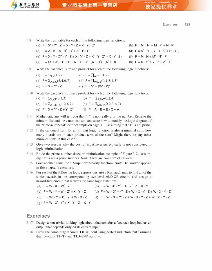
Exercises 129
3.8 Write the truth table for each of the following logic functions:
3.9 Write the canonical sum and product for each of the following logic functions:
3.10 Write the canonical sum and product for each of the following logic functions:
3.11 Mathematicians will tell you that “1” is not really a prime number. Rewrite theminterm list and the canonical sum and state how to modify the logic diagram ofthe prime-number-detector example on page 111, assuming that “1” is not prime.
3.12 If the canonical sum for an n-input logic function is also a minimal sum, howmany literals are in each product term of the sum? Might there be any otherminimal sums in this case?
3.13 Give two reasons why the cost of input inverters typically is not considered inlogic minimization.
3.14 Re-do the prime-number-detector minimization example of Figure 3-24, assum-ing “1” is not a prime number. Hint: There are two correct answers.
3.15 Give another name for a 2-input even-parity function. Hint: The answer appearsin this chapter’s exercises.
3.16 For each of the following logic expressions, use a Karnaugh map to find all of thestatic hazards in the corresponding two-level AND-OR circuit, and design ahazard-free circuit that realizes the same logic function:
Exercises3.17 Design a non-trivial-looking logic circuit that contains a feedback loop but has an
output that depends only on its current input.
3.18 Prove the combining theorem T10 without using perfect induction, but assumingthat theorems T1–T9 and T1D–T9D are true.
(a) F = X′ ⋅ Y′ ⋅ Z′ + X ⋅ Y ⋅ Z + X ⋅ Y′ ⋅ Z′ (b) F = M′ ⋅ N′ + M ⋅ P′ + N ⋅ P′(c) F = A ⋅ B + A ⋅ B′ ⋅ C′ + A′ ⋅ B ⋅ C′ (d) F = A′ ⋅ B ⋅ (C ⋅ B ⋅ A′ + B′ ⋅ C′)(e) F = X ⋅ Y ⋅ (X′ ⋅ Y ⋅ Z + X ⋅ Y′ ⋅ Z + X′ ⋅ Y ⋅ Z′ + X ⋅ Y ⋅ Z) (f) F = M ⋅ N + M′ ⋅ N′ ⋅ P
(g) F = (A + A′) ⋅ B + B′ ⋅ A ⋅ C + C′ ⋅ (A + B′) ⋅ (A′ + B) (h) F = X ⋅ Y′ + Y ⋅ Z + Z′ ⋅ X′
(a) F = ΣX,Y(1,2) (b) F = ∏A,B(0,1,2)
(c) F = ΣA,B,C(2,4,6,7) (d) F = ∏W,X,Y(0,1,3,4,5)
(e) F = X + Y′ ⋅ Z′ (f) F = V′ + (W′ ⋅ X)′
(a) F = ΣX,Y,Z(0,1,3) (b) F = ∏A,B,C(0,2,4)
(c) F = ΣA,B,C,D(1,2,6,7) (d) F = ∏M,N,P(0,2,3,6,7)
(e) F = X + Y′ ⋅ Z + Y ⋅ Z′ (f) F = A′ ⋅ B + B ⋅ C + A
(a) F = W ⋅ X + W′ ⋅ Y′ (b) F = W ⋅ X′ ⋅ Y′ + X ⋅ Y′ ⋅ Z + X ⋅ Y
(c) F = W ⋅ Y + W′ ⋅ Z′ + X ⋅ Y′ ⋅ Z (d) F = W′ ⋅ X′ + Y′ ⋅ Z + W′ ⋅ X ⋅ Y ⋅ Z + W ⋅ X ⋅ Y ⋅ Z′(e) F = W′ ⋅ Y + X′ ⋅ Y′ + W ⋅ X ⋅ Z (f) F = W′ ⋅ X + Y′ ⋅ Z + W ⋅ X ⋅ Y ⋅ Z + W ⋅ X′ ⋅ Y ⋅ Z′(g) F = W ⋅ X′ ⋅ Y′ + X ⋅ Y′ ⋅ Z + X ⋅ Y
DDPP5.book Page 129 Tuesday, March 28, 2017 5:33 PM

130 Chapter 3 Switching Algebra and Combinational Logic
3.19 Prove that (X + Y′) ⋅ Y = X ⋅ Y without using perfect induction. You may assumethat theorems T1–T11 and T1D–T11D are true.
3.20 Prove that (X + Y) ⋅ (X′ + Z) = X ⋅ Z + X′ ⋅ Y without using perfect induction. Youmay assume that theorems T1–T11 and T1D–T11D are true.
3.21 Show that an n-input OR gate can be replaced by (n−1) 2-input OR gates. Can thesame statement be made for NOR gates? Justify your answer.
3.22 How many physically different ways are there to realize V ⋅ W ⋅ X ⋅ Y ⋅ Z usingfour 2-input AND gates? Justify your answer.
3.23 Use switching algebra to prove that tying together two inputs of an (n+1)-inputAND or OR gate gives it the functionality of an n-input gate.
3.24 Prove DeMorgan’s theorems (T13 and T13D) using finite induction.
3.25 Use the theorems of switching algebra to rewrite the following expression usingas few terms and inversions as possible (complemented parentheses are allowed):
3.26 Prove Shannon’s expansion theorems. (Hint: Don’t get carried away; it’s easy.)
3.27 The generalized Shannon expansion theorems “pull out” not just one but i vari-ables so that a logic function can be expressed as a sum or product of 2 i terms.Figure out and state the generalized Shannon expansion theorems.
3.28 Show how the generalized Shannon expansion theorems lead to the canonicalsum and canonical product representations of logic functions.
3.29 Prove or disprove the following propositions:
(a) Let A and B be switching-algebra variables. Then A ⋅ B = 0 and A + B = 1 implies that A = B′.
(b) Let X and Y be switching-algebra expressions. Then X ⋅ Y = 0 and X + Y = 1 implies that X = Y′.
3.30 An Exclusive OR (XOR) gate is a 2-input gate whose output is 1 if and only ifexactly one of its inputs is 1. Write a truth table, sum-of-products expression, andcorresponding AND-OR circuit for the Exclusive OR function.
3.31 An Exclusive NOR (XNOR) gate is a 2-input gate whose output is 1 if and only ifboth of its inputs are equal. Write a truth table, sum-of-products expression, andcorresponding AND-OR circuit for the Exclusive NOR function.
3.32 From the point of view of switching algebra, what is the function of a 2-inputXNOR gate whose inputs are tied together? How might the output behavior of areal XNOR gate differ?
3.33 Any set of logic-gate types that can realize any logic function is called a completeset of logic gates. For example, 2-input AND gates, 2-input OR gates, andinverters are a complete set, because any logic function can be expressed as a sumof products of variables and their complements, and AND and OR gates with anynumber of inputs can be made from 2-input gates. Do 2-input NOR gates form acomplete set of logic gates? Prove your answer.
3.34 Do 2-input AND gates which have one input inverted form a complete set of logicgates? Prove your answer. Why might this type of gate be called an “inhibit” gate?Does this mean that a standard AND gate could be called “uninhibited”?
B′ ⋅ C + A ⋅ C ⋅ D′ + A′ ⋅ C + D ⋅ B′ + E ⋅ (A + C) ⋅ (A′ + D′)
generalized Shannon-expansion theorems
Exclusive OR (XOR) gate
Exclusive NOR (XNOR) gate
complete set
DDPP5.book Page 130 Tuesday, March 28, 2017 5:33 PM

Exercises 131
3.35 Do 2-input XOR gates form a complete set of logic gates? Prove your answer.3.36 For each of the following descriptions of a combinational logic function, name
the function’s inputs and output and give their meanings. Then, fully specify thefunction using a truth table or logic equations. In the second approach, you mayuse intermediate variables if they are useful to simplify the problem.
3.37 Some people think that there are four basic logic functions, AND, OR, NOT, andBUT. Figure X3.37 is a possible symbol for a 4-input, 2-output BUT gate. Inventa useful, nontrivial function for the BUT gate to perform. The function shouldhave something to do with the name (BUT). Keep in mind that, due to the sym-metry of the symbol, the function should be symmetric with respect to the A andB inputs of each section and with respect to sections 1 and 2. Describe your BUT’sfunction and write its truth table.
3.38 Write logic expressions for the Z1 and Z2 outputs of the BUT gate you designedin the preceding exercise, and draw a corresponding logic diagram using ANDgates, OR gates, and inverters.
3.39 How many different nontrivial logic functions are there of n variables? Here,“nontrivial” means that all of the variables affect the output.
3.40 Most students have no problem using theorem T8 to “multiply out” logic expres-sions, but many develop a mental block if they try to use theorem T8D to “addout” a logic expression. How can duality be used to overcome this problem?
3.41 Describe how to adapt any software tool that synthesizes AND-OR logic insteadto synthesize OR-AND logic.
3.42 Prove that .
3.43 A self-dual logic function is a function F such that F = FD. Which of the followingfunctions are self-dual? (The symbol ⊕ denotes the Exclusive OR (XOR)operation.)
(a) Specify the on/off control signal for the dome light in a typical car.
(b) Specify a signal that is 1 if and only if two 2-bit numbers N and M are equal.
(c) In a certain nerdy family, each person P is identified by their generation PG (0 being the parents) and their sex PS (for simplicity, just one bit, please); each child was also given a unique 2-bit identifier PN at birth, starting at 00. Specify a function that is 1 if and only if person P is a daughter of person Q.
(d) Repeat problem (c) for a function that is 1 if and only if person P is the father of person Q.
(e) Repeat problem (c) for a function that is 1 if and only if person P is a younger brother of person Q.
(f) Repeat problem (c) for a function that is 1 if and only if persons P and Q are the parents.
(a) F = X (b) F = ΣX,Y,Z(0,3,5,6)
(c) F = X ⋅ Y + X Y (d) F = W ⋅ (X⊕Y⊕Z) + W (X⊕Y⊕Z)
(e) A function F of 7 variables such that F = 1 if and only if 4or more of the variables are 1
(f) A function F of 10 variables suchthat F = 1 if and only if 5 or moreof the variables are 1
BUTBUT gate
A1
B1
A2
B2
Z1
Z2
Figure X3.37
FD X1 X, 2 … Xn, ,( ) F X1 X, 2 Xn, ,[ ]=
self-dual logic function
DDPP5.book Page 131 Tuesday, March 28, 2017 5:33 PM

132 Chapter 3 Switching Algebra and Combinational Logic
3.44 Assuming the signal delay through NAND gates and inverters is 5 ns, NOR gatesis 6 ns, and noninverting gates is 9 ns, what is the total delay to the slowest outputin each of the circuits in Figure 3-21(a), (c), and (d).
3.45 How many self-dual logic functions of n input variables are there? (Hint:Consider the structure of the truth table of a self-dual function.)
3.46 Prove that any n-input logic function F(X1,…, Xn) that can be written in the formF = X1 ⋅ G(X2,…,Xn) + X1′ ⋅ GD(X2,…,Xn) is self-dual.
3.47 Assign variables to the inputs of the AND-XOR circuit in Figure X3.47 so that itsoutput is F = ΣW,X,Y,Z(6,7,12,13). You may use a Karnaugh map if it helps you.What is the solution if the AND gates are changed to NAND gates?
3.48 A distinguished 1-cell in a logic function’s Karnaugh map is a cell (and a corre-sponding input combination) that is covered by only one prime implicant. Suchan essential prime implicant must be present in any minimal sum for the function.Thus, an efficient minimization algorithm looks first for essential prime impli-cants, and then selects additional prime implicants only as needed for 1-cells thatare still uncovered, if any. The following logic functions all have one or moreessential prime implicants; find their minimal sums:
3.49 A 3-bit “comparator” circuit receives two 3-bit numbers, P = P2P1P0 and Q =Q2Q1Q0. Design a minimal sum-of-products circuit that produces a 1 output ifand only if P < Q.
3.50 Algebraically prove whether or not the following expression is minimal. That is,can any product term be eliminated and if not, can any input be removed from anyproduct term?
3.51 Exhibit a 4-input logic function, other than the one in Figure 3-25, whose Kar-naugh map is a “checkerboard” with eight minterms. Does this logic functionhave a concise name?
3.52 (Hamlet circuit.) Complete the timing diagram and explain the function of the cir-cuit in Figure X3.52. Where does the circuit get its name?
3.53 Prove that a two-level AND-OR circuit corresponding to the complete sum of alogic function is always hazard free.
(a) F = ΣX,Y,Z(1,3,5,6,7) (b) F = ΣW,X,Y,Z(1,4,5,6,7,9,14,15)
(c) F = ∏W,X,Y(1,4,5, 6, 7) (d) F = ΣW,X,Y,Z(0,1,6,7,8,9,14,15)
(e) F = ∏A,B,C,D(4, 5, 6, 13,15) (f) F = ΣA,B,C,D(4,5,6, 11, 13,14,15)
F = C ⋅ D ⋅ E′ ⋅ F′ ⋅ G + B ⋅ C ⋅ E ⋅ F′ ⋅ G + A ⋅ B ⋅ C ⋅ D ⋅ F′ ⋅ G
Figure X3.47
distinguished 1-cell
essential prime implicant
2BF 2B
FFigure X3.52
DDPP5.book Page 132 Tuesday, March 28, 2017 5:33 PM