switchable and tunable bulk acoustic wave resonators based...
TRANSCRIPT
Thesis for the degree of Doctor of Philosophy
Switchable and tunable bulk acoustic wave
resonators based on BaxSr1−xTiO3 thin films
John Berge
Terahertz and Millimetre Wave LaboratoryDepartment of Microtechnology and Nanoscience (MC2)
Chalmers University of TechnologyGoteborg, Sweden, 2012

Switchable and tunable bulk acoustic wave resonatorsbased on BaxSr1−xTiO3 thin films
John BergeISBN 978-91-7385-643-0
© John Berge, 2012
Doktorsavhandlingar vid Chalmers tekniska hogskola
Ny serie #3324
ISSN 0346-718X
Technical Report MC2-215
ISSN 1652-0769
Chalmers University of Technology
Department of Microtechnology and Nanoscience (MC2)
Terahertz and Millimetre Wave Laboratory
SE–412 96 Goteborg, Sweden
Phone: +46 (0) 31 772 1000
Cover: Smith chart showing response of Ba0.25Sr0.75TiO3 TFBAR at different
dc bias voltages.
Printed by Chalmers Reproservice
Goteborg, Sweden, 2012
Abstract
The main focus of this thesis is the study of a novel microwavecomponent, the tunable thin film bulk acoustic wave resonator(TFBAR), based on ferroelectric BaxSr1−xTiO3 thin films.
Conventional fixed frequency TFBARs, widely used for filter-ing applications in wireless communication systems, are based onordinary piezoelectrics. The tunable TFBAR on the other handutilizes the dc field induced piezoelectric effect in the ferroelec-tric film. This allows dc field tuning of the resonance frequencyas well as switching between resonator and capacitor response.
A brief introduction to the BaxSr1−xTiO3 material systemis given, followed by results from thin films grown by pulsedlaser deposition. Effects of substrate temperature and ambientgas pressure during growth are discussed.
Resonator design and fabrication issues are covered, includingstudies of electrode configurations and acoustic mirror structures.Measurement results are presented in wide dc bias and temper-ature ranges. The achieved room temperature tuning range fora 5.7 GHz Ba0.25Sr0.75TiO3 TFBAR is 3.8% and the effectiveelectromechanical coupling coefficient at maximum bias is 7.1%,with a Q-factor of 130.
A switchable bandpass filter is considered as a possible appli-cation of BaxSr1−xTiO3 TFBARs. Simulated filter characteristicsand preliminary results from fabricated filters are presented.
Keywords: Ferroelectric thin films, tunable microwave devices,bulk acoustic wave devices, piezoelectric resonators, field inducedpiezoelectric effect.
i


List of publications
Appended papers
[A] J. Berge, A. Vorobiev, and S. Gevorgian, “Impact of thin film rough-ness on the performance of tunable bulk acoustic wave resonators,”Manuscript.
[B] J. Berge and S. Gevorgian, “Tunable bulk acoustic wave resonatorsbased on Ba0.25Sr0.75TiO3 thin films and a HfO2/SiO2 Bragg re-fector,” IEEE Trans. Ultrason. Ferroelectr. Freq. Control, vol. 58,no. 12, pp. 2768–2771, 2011.
[C] J. Berge, M. Norling, A. Vorobiev, and S. Gevorgian, “The effect ofBragg reflectors on the electromechanical performance of parallel-plate ferroelectric capacitors,” IOP Conf. Ser.: Mater. Sci. Eng.,vol. 8, no. 1, pp. 012011–1–4, 2010.
[D] J. Berge, M. Norling, A. Vorobiev, and S. Gevorgian, “Field andtemperature dependent parameters of the dc field induced reso-nances in BaxSr1−xTiO3-based tunable thin film bulk acoustic res-onators,” J. Appl. Phys., vol. 103, no. 6, pp. 064508–1–8, 2008.
[E] J. Berge, A. Vorobiev, W. Steichen, and S. Gevorgian, “Tun-able solidly mounted thin film bulk acoustic resonators basedon BaxSr1−xTiO3 films,” IEEE Microw. Wireless Compon. Lett.,vol. 17, no. 9, pp. 655–657, 2007.
[F] J. Berge, A. Vorobiev, and S. Gevorgian, “The effect of growthtemperature on the nanostructure and dielectric response ofBaTiO3 ferroelectric films,” Thin Solid Films, vol. 515, no. 16,pp. 6302–6308, 2007.
iii

Other publications
[a] A. Vorobiev, J. Berge, S. Gevorgian, M. Loffler, and E. Olsson,“Effect of interface roughness on acoustic loss in tunable thin filmbulk acoustic wave resonators,” J. Appl. Phys., vol. 110, no. 2,pp. 024116–1–4, 2011.
[b] A. Vorobiev, J. Berge, M. Norling, and S. Gevorgian, “Siliconsubstrate integration of BST based tunable TFBARs using all-dielectric SiO2/AlN Bragg reflectors,” in Proc. IEEE SiRF, 2010,pp. 41–44.
[c] M. Norling, J. Berge, and S. Gevorgian, “Parameter extraction fortunable TFBARs based on BaxSr1−xTiO3,” in IEEE MTT-S Int.Microw. Symp. Dig., 2009, pp. 101–104.
[d] S. Gevorgian, T. Lewin, A. Vorobiev, M. Norling, and J. Berge,“A voltage controlled switching device”, Patent WO/2009/043370(April 9 2009), Int. filing date Oct 1 2007.
[e] I. B. Vendik, P. A. Turalchuk, O. G. Vendik, and J. Berge, “Mod-eling tunable bulk acoustic resonators based on induced piezoelec-tric effect in BaTiO3 and Ba0.25Sr0.75TiO3 films,” J. Appl. Phys.,vol. 103, no. 1, pp. 014107–1–6, 2008.
[f] P. Turalchuk, I. Vendik, O. Vendik, and J. Berge, “Electrically tun-able bulk acoustic filters with induced piezoelectric effect in BSTOfilm,” in Proc. EuMC, 2008, pp. 1695–1698.
[g] A. Vorobiev, J. Berge, and S. Gevorgian, “Thin filmBa0.25Sr0.75TiO3 voltage tunable capacitors on fused silicasubstrates for applications in microwave microelectronics,”Thin Solid Films, vol. 515, no. 16, pp. 6606–6610, 2007.
[h] P. Turalchuk, I. Vendik, O. Vendik, and J. Berge, “Modelling oftuneable acoustic resonators based on BSTO films with inducedpiezoelectric effect,” in Proc. EuMC, 2007, pp. 282–285.
[i] A. Vorobiev, J. Berge, and S. Gevorgian, “Thin filmBa0.25Sr0.75TiO3 varactors on Au bottom electrode for microwaveapplications,” in Proc. EuMC, 2006, pp. 839–842.
[j] S. Gevorgian, A. Vorobiev, and J. Berge, “Electromechanical Mod-elling and Reduction of the Electroacoustic Losses in Parallel-PlateFerroelectric Varactors,” in Proc. EuMC, 2006, pp. 851–853.
iv
Contents
Abstract i
List of publications iii
1 Introduction 11.1 Motivation and thesis organization . . . . . . . . . . . . 11.2 Ferroelectricity and related properties . . . . . . . . . . 21.3 BaxSr1−xTiO3 . . . . . . . . . . . . . . . . . . . . . . . 3
2 Ferroelectric thin films 72.1 Thin film technologies . . . . . . . . . . . . . . . . . . . 72.2 Laser ablated ferroelectric films . . . . . . . . . . . . . . 9
2.2.1 Impact of substrate temperature . . . . . . . . . 122.2.2 Impact of oxygen pressure . . . . . . . . . . . . . 15
3 Tunable thin film bulk acoustic wave resonators 193.1 Introduction . . . . . . . . . . . . . . . . . . . . . . . . . 193.2 Design and fabrication . . . . . . . . . . . . . . . . . . . 21
3.2.1 Bragg reflector . . . . . . . . . . . . . . . . . . . 233.2.2 Electrodes . . . . . . . . . . . . . . . . . . . . . . 25
3.3 Measurement results . . . . . . . . . . . . . . . . . . . . 283.3.1 De-embedding procedure . . . . . . . . . . . . . 283.3.2 Resonators with Au/SiO2 reflector and Au bot-
tom electrode . . . . . . . . . . . . . . . . . . . . 293.3.3 Resonators with HfO2/SiO2 reflector and Pt bot-
tom electrode . . . . . . . . . . . . . . . . . . . . 313.4 Modeling and theory of induced piezoeffect . . . . . . . 333.5 Temperature dependence studies . . . . . . . . . . . . . 373.6 Resonator performance . . . . . . . . . . . . . . . . . . . 39
3.6.1 Q-factor reduction mechanisms . . . . . . . . . . 403.7 Conclusions . . . . . . . . . . . . . . . . . . . . . . . . . 42
4 Switchable filter 454.1 Filter design and simulation . . . . . . . . . . . . . . . . 454.2 Fabrication and measurements . . . . . . . . . . . . . . 46
v
5 Summary and outlook 515.1 Summary of appended papers . . . . . . . . . . . . . . . 52
Acknowledgments 55
Bibliography 57
vi

Chapter 1
Introduction
This introductory chapter provides motivation for the work presentedin this thesis, and a description of the thesis organization. Some back-ground to the ferroelectric materials under consideration in this work isalso given.
1.1 Motivation and thesis organization
This thesis is devoted to the study of ferroelectric BaxSr1−xTiO3 thinfilms and their use in tunable microwave devices. Reconfigurable tech-nologies are expected to become increasingly important in order to meetpresent and future demands on improved and added functionalities ofmicrowave devices. Modern mobile phones is an example where the com-bination of multi-standard cellular network capabilities, GPS receiversand WLAN connectivity, all operating in separate frequency bands, setstrict requirements on the rf design.
The main focus of this work is a novel type of thin film bulk acousticwave resonator (TFBAR) which due to the field dependent properties ofthe ferroelectric material presents switchable and tunable characteristicsunder dc bias. The principal functionality of this component has onlyrecently been demonstrated, and it may potentially contribute to morecost effective, energy efficient, and compact microwave systems. Thistype of resonator may allow development of switchable filters which cansimplify the signal path in multi-standard communication systems byeliminating separate switches. Truly tunable bandpass filters could bringeven further advantages by replacing several fixed frequency filters andswitches with one compact component. Another attractive application oftunable TFBARs is voltage controlled oscillators, where the potentiallyvery high Q-factor of the tunable TFBAR could replace LC tanks basedon lossy varactors.
The work presented mainly concerns development and studies of theresonator itself, including issues related to resonator design, fabrication
1

2 CHAPTER 1. INTRODUCTION
Fig. 1.1: The general class of dielectrics can be divided into subgroupsof piezoelectric, pyroelectric and ferroelectric materials.
and characterization. The thesis is organized as follows. This chaptergives a brief background to the concept of ferroelectricity and intro-duces BaxSr1−xTiO3 (BSTO), the ferroelectric material system underconsideration in this thesis. Chapter 2 gives an introduction to BSTOthin film technologies and summarizes some results on laser ablatedBSTO thin films characterized using parallel plate varactor structures.Chapter 3 constitutes the core of the thesis and discusses the actualBSTO TFBAR studies. Chapter 4 discusses preliminary results of afabricated switchable ladder filter based on BSTO TFBARs. A briefsummary and concluding remarks are given in Chapter 5.
1.2 Ferroelectricity and related properties
In this section a brief introduction to the concept of ferroelectricity isgiven. The relation between ferroelectrics, ordinary dielectrics, piezo-electrics and pyroelectrics is described.
Fig. 1.1 schematically shows how the general class of dielectrics (in-sulators) can be divided into subgroups of piezoelectric, pyroelectric andferroelectric materials. From symmetry considerations all possible crys-tal structures can be divided into 32 crystal classes or crystallographicpoint groups. Out of these 32 crystal classes 11 are centrosymmetric,i.e. they contain a center of inversion symmetry which inhibits the crys-tal from having polar properties.
The remaining 21 crystal classes are all non-symmetric, allowingthe crystal to contain one or more polar axes. All but one of the non-symmetric crystal classes exhibit the piezoelectric effect, i.e. a couplingbetween the electrical and mechanical systems which allows electricalenergy to be transformed to mechanical energy and vice versa. In piezo-electric materials an applied mechanical stress results in polarizationcharges at the crystal surfaces (direct piezoelectric effect) and an appliedelectric field causes the material to change its shape (converse piezoelec-tric effect). Piezoelectricity is linear, if the sign of the applied field isreversed the response is also reversed. Centrosymmetric materials also

1.3. BSTO 3
Ba (A)
Ti (B)
O
Fig. 1.2: Cubic BaTiO3 unit cell. (General perovskite, ABO3.)
change their shape slightly as an electric field is applied through the ef-fect known as electrostriction, present in all dielectrics. In contrast to theconverse piezoelectric effect electrostriction is quadratic with the appliedfield, or more correctly with the induced polarization [1], i.e. reversingthe field results in the same mechanical response. The electrostrictiveeffect is very weak for most materials but can in some cases, such asBaxSr1−xTiO3, be considerable, as will be discussed in chapter 3.
10 of the 20 piezoelectric crystal classes reveal a spontaneous polar-ization in absence of an external electric field. The spontaneous polar-ization charges on the crystal surface change with temperature and thegroup of crystals are said to exhibit the pyroelectric effect. If in addi-tion the direction of the spontaneous polarization can be switched byan external electric field, the crystal is said to be ferroelectric.
1.3 BaxSr1−xTiO3
One of the most well known ferroelectric materials is BaTiO3. BaTiO3
crystallizes in the perovskite structure and undergoes a series of phasetransitions with increasing temperature, from rhombohedric to ortho-rhombic to tetragonal structures, all of which are ferroelectric. Above120◦C [2] the material enters a centrosymmetric, non-ferroelectric cubicphase, referred to as the paraelectric phase. Fig. 1.2 shows the cubicBaTiO3 unit cell. The Ti ion in the center of the unit cell is too smallto completely fill the space created by the Ba-O ions, and hence is eas-ily displaced from the center, leading to a high permittivity. The lowersymmetry phases can be seen as an attempt to minimize the size ofthe Ti cavity, resulting in a displacement of the Ti ion and thus a netpolarization [3].
For applications in tunable microwave devices the paraelectric phaseis generally of most interest. This phase reveals strongly field dependentproperties (e.g. relative permittivity) without the additional loss mecha-nisms and hysteresis effects present in ferroelectric phases. As mentionedabove, the transition temperature, or Curie temperature, from the cu-

4 CHAPTER 1. INTRODUCTION
bic paraelectric phase to the ferroelectric tetragonal phase is 120◦C forBaTiO3, and the material is thus ferroelectric at room temperature.To lower the Curie temperature BaTiO3 can be combined in a solidsolution with SrTiO3, which is a so-called incipient ferroelectric, alsowith the perovskite crystal structure. Incipient ferroelectrics, or quan-tum paraelectrics, are materials whose properties resemble those of aferroelectric in the paraelectric phase, but never reaches a ferroelec-tric phase transition even at very low temperatures. SrTiO3 is cubicand centrosymmetric at room temperature and undergoes a structuralphase transition with reducing temperature to a tetragonal phase at105K [2]. In contrast to the tetragonal phase of BaTiO3, this phase ishowever still centrosymmetric, and the material is paraelectric for alltemperatures. BaTiO3 and SrTiO3 form a solid solution BaxSr1−xTiO3
(BSTO) for all compositions x, and the Curie temperature decreasesalmost linearly with increasing Sr concentration [4]. This is very usefulfrom an application point of view since important material parameterssuch as permittivity, which are strongly dependent on the Curie temper-ature, can be tailored in a wide range by choosing a material with theappropriate composition x. It can be noted that BSTO above the Curietemperature (in the paraelectric phase) does not exhibit the ferroelectricand piezoelectric properties as discussed above, but is still commonlyreferred to as a ferroelectric material.
Fig. 1.3 shows the temperature dependence of the relative permit-tivity for ceramic BSTO with varying Ba/Sr content. The phase transi-tion is accompanied by a dramatic increase of the permittivity. Aboveand below this peak the material reveals paraelectric and ferroelectricproperties, respectively. The shift of the transition temperature with in-creasing Sr content can be clearly seen, indicating that more than 30%Sr is needed in order for the material to be paraelectric at room tem-perature. Fig. 1.4 shows schematic dependences of the polarization as afunction of electric field. The paraelectric phase presents field dependentproperties (e.g. permittivity, slope of the P-E plot) allowing tunability,but is free of hysteresis.

1.3. BSTO 5
Fig. 1.3: Relative permittivity of ceramic BaxSr1−xTiO3 as a functionof temperature, for different Ba concentration x. From [5].
(a) (b)
Fig. 1.4: Schematic representation of polarization as a function of elec-tric field for material in ferroelectric phase (a) and paraelectric phase(b).


Chapter 2
Ferroelectric thin films
Ferroelectric ceramics have been used for high density capacitors andpiezoelectric transducers since the 1940s [6]. Since then tunable highfrequency devices have been demonstrated using both bulk ferroelec-tric ceramics and single crystals, as well as thick ceramic films includingHTCC and LTCC technologies [7]. Inspired by the integrated circuit de-velopment, thin film materials emerged during the 1970s and 1980s [6]and have been extensively studied until today, aiming at non-volatilememory applications [8], sensors and actuators [9, 10], as well as tun-able microwave components [7]. The electric fields required to obtainappreciable tuning is easily achieved at relatively low bias voltages withmaterial in thin film form, and possibilities for small size, silicon inte-grated components are attractive.
2.1 Thin film technologies
Several thin film deposition technologies have been used and reported inthe literature for the synthesis of ferroelectric films. Brief descriptionsof the most common and successful methods are given below.
MOCVD (Metalorganic chemical vapor deposition), originally de-veloped for epitaxial growth of compound semiconductor materials, is agrowth technique capable of producing high quality thin films of variousmaterials including metals and ferroelectrics [11]. Complex metalorganicsource materials, precursors, are introduced into the growth chamber ingas form and react on a heated substrate to form the solid thin film.Growth rate and composition are controlled by adjusting the mass flowrate of the different gases. MOCVD has been shown to be able to pro-duce BaxSr1−xTiO3 films with very good composition control, uniformlarge area coverage, and beneficial columnar microstructure [7]. Exam-ples of precursors for growth of BaxSr1−xTiO3 films are Ti(OPr)2(thd)2,Ba(thd)2, Sr(thd)2, where Pr=propyl and thd=2,2,6,6-tetramethyl-3,5-heptanedionate [11].
7
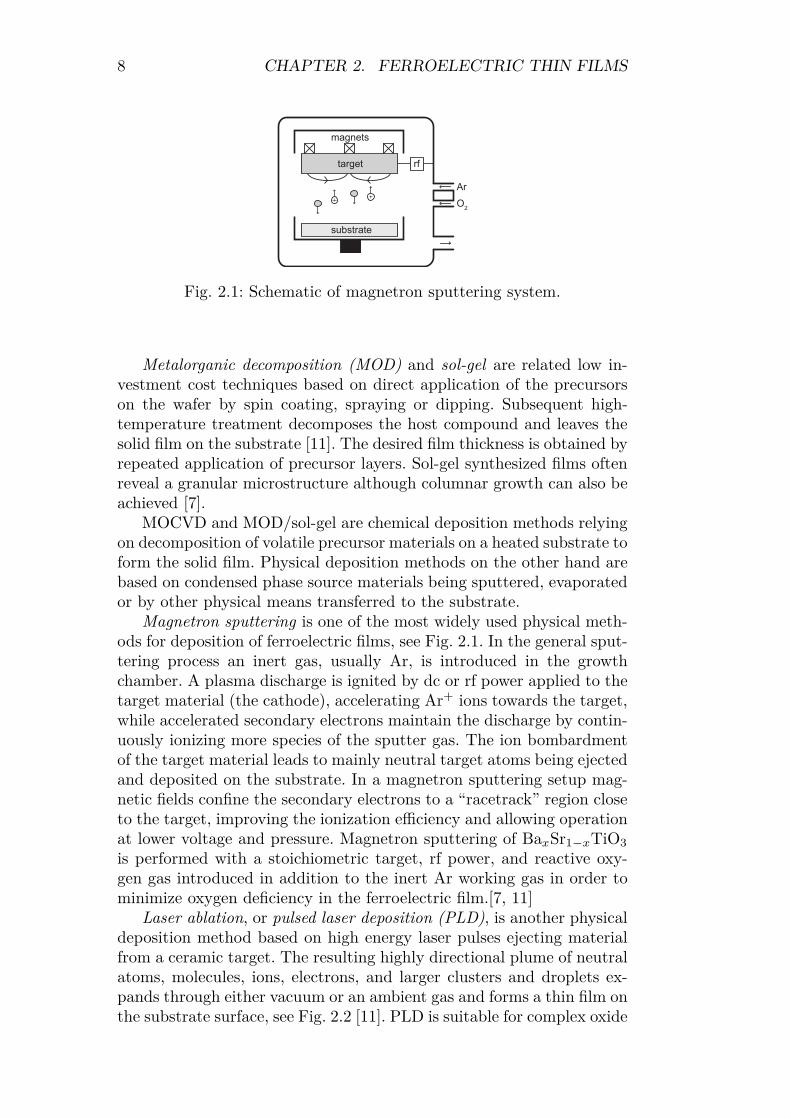
8 CHAPTER 2. FERROELECTRIC THIN FILMS
Fig. 2.1: Schematic of magnetron sputtering system.
Metalorganic decomposition (MOD) and sol-gel are related low in-vestment cost techniques based on direct application of the precursorson the wafer by spin coating, spraying or dipping. Subsequent high-temperature treatment decomposes the host compound and leaves thesolid film on the substrate [11]. The desired film thickness is obtained byrepeated application of precursor layers. Sol-gel synthesized films oftenreveal a granular microstructure although columnar growth can also beachieved [7].
MOCVD and MOD/sol-gel are chemical deposition methods relyingon decomposition of volatile precursor materials on a heated substrate toform the solid film. Physical deposition methods on the other hand arebased on condensed phase source materials being sputtered, evaporatedor by other physical means transferred to the substrate.
Magnetron sputtering is one of the most widely used physical meth-ods for deposition of ferroelectric films, see Fig. 2.1. In the general sput-tering process an inert gas, usually Ar, is introduced in the growthchamber. A plasma discharge is ignited by dc or rf power applied to thetarget material (the cathode), accelerating Ar+ ions towards the target,while accelerated secondary electrons maintain the discharge by contin-uously ionizing more species of the sputter gas. The ion bombardmentof the target material leads to mainly neutral target atoms being ejectedand deposited on the substrate. In a magnetron sputtering setup mag-netic fields confine the secondary electrons to a “racetrack” region closeto the target, improving the ionization efficiency and allowing operationat lower voltage and pressure. Magnetron sputtering of BaxSr1−xTiO3
is performed with a stoichiometric target, rf power, and reactive oxy-gen gas introduced in addition to the inert Ar working gas in order tominimize oxygen deficiency in the ferroelectric film.[7, 11]
Laser ablation, or pulsed laser deposition (PLD), is another physicaldeposition method based on high energy laser pulses ejecting materialfrom a ceramic target. The resulting highly directional plume of neutralatoms, molecules, ions, electrons, and larger clusters and droplets ex-pands through either vacuum or an ambient gas and forms a thin film onthe substrate surface, see Fig. 2.2 [11]. PLD is suitable for complex oxide

2.2. LASER ABLATED FERROELECTRIC FILMS 9
O2
rotatingtarget substrate
on heater
plume
laser
Fig. 2.2: Schematic of laser ablation system.
materials such as high temperature superconductors and ferroelectricsdue to the highly stoichiometric transport of material from the targetto the substrate surface. The relative simplicity of the system combinedwith possibilities to vary the growth parameters in a wide range, andto share one laser between several growth chambers, makes laser abla-tion suitable for research environments for synthesis of complex or novelmaterials and multilayers. A disadvantage of the conventional PLD tech-nique is the limited size of substrates. Special arrangements using scan-ning of the laser beam and rotation/translation of the substrate havehowever been developed allowing large area depositions [7]. Dependingon deposition conditions and choice of substrate material, magnetronsputtering and laser ablation can produce ferroelectric films with var-ious microstructure, ranging from high quality epitaxial and texturedcolumnar films to amorphous films.
Irrespective of deposition technology some differences are observedwhen comparing the properties of thin films with their bulk mate-rial ceramic or single crystal counterparts. Most markedly the strongpeak in the permittivity accompanying the ferroelectric phase transi-tion (Fig. 1.3) is for thin film materials generally severely damped, andshifted towards lower temperatures. The resulting overall permittivityreduction, the strength of which depends on the film thickness, is typicalfor thin film ferroelectrics. Higher dielectric losses due to film imperfec-tions, oxygen vacancies, grain boundaries, etc. are also characteristicof many films. This degradation of material properties of course sets alimit to the performance of thin film devices and the origin and processesbehind it is therefore of highest interest.
2.2 Laser ablated ferroelectric films
In this work BSTO films have been grown by PLD on metalized highresistivity Si substrates. In this section some general results from thesefilms are discussed, as characterized using parallel plate varactor teststructures.

10 CHAPTER 2. FERROELECTRIC THIN FILMS
For parallel plate structures the bottom electrode is crucial since itforms the template for the BSTO film growth. The generally acceptedelectrode material of choice for growth of BSTO films is Pt, which issufficiently inert in order to withstand the high temperature oxidizingconditions. Pt electrodes also promote low leakage currents through theferroelectric film under dc bias. This effect can be explained by the gen-eral model of BSTO as a wide band gap semiconductor/dielectric withlow carrier concentration [12]. In such a system barriers are formed atthe metal/BSTO interfaces, and the barrier height is mainly determinedby the work function of the contacting metal. High work function Ptat the cathode would thus result in a high barrier to charge injection,and low leakage currents, while lower work function metals such as Tior Al would be less favourable in this respect. This is in line with qual-itative observations made for various contact metals throughout thiswork. Conductive oxide electrodes such as SrRuO3, which may have mi-crostructural advantages over metal electrodes, are generally considerednot to be an option for room temperature high frequency applicationsdue to their limited conductivity and lower barrier to charge injection.
In this work growth of BSTO thin films have been carried out intwo different PLD systems, both equipped with a KrF excimer laseremitting 248 nm wavelength 30 ns pulses. The laser pulses are focusedinto a 1×4 mm2 spot on a rotating 12 mm diameter ceramic target,ablating material onto the heated substrate in an on-axis configuration.O2 is used as reactive gas during all depositions.
The ferroelectric film microstructure has been studied using scanningelectron microscopy (SEM), atomic force microscopy (AFM) and X-ray diffraction (XRD). A typical SEM cross section image can be seenin Fig. 2.3a, revealing a pronounced columnar structure with grainsextending through the film thickness. The lateral size of these columnscan be estimated from AFM images of the film surface, Fig. 2.3b, tobe approximately 30 nm (confirmed by TEM studies [13]). XRD θ-2θscans, Fig. 2.4, show a mixed phase content of the ferroelectric film.(100) and (110) phases are clearly present, while a possible (111) phaseis masked by strong reflections from thick (111) textured Au electrodes.
Below results from BaTiO3 based parallel plate varactor test struc-tures will be discussed, emphasizing how the PLD growth parame-ters affect the properties of the resulting film, and highlighting a fewgeneral ferroelectric thin film characteristics. The varactors are fabri-cated on platinized high resistivity Si substrates, with evaporated Au/Pt(500/50 nm) bottom and top electrodes sandwiching the ferroelectricfilm. The thick Au layers minimize the electrode related losses at higherfrequencies [14]. The top electrode (1, Fig. 2.5) consists of a circularpatch, 30 μm or 10 μm in diameter, while the non-patterned bottomelectrode (2, Fig. 2.5) is capacitively contacted through a large areatop electrode, effectively creating a parallel plate capacitor suitable formeasurements with ground-signal-ground microprobes. This simple de-

2.2. LASER ABLATED FERROELECTRIC FILMS 11
(a) (b)
Fig. 2.3: Typical SEM cross section image (a) and AFM surface image(b) of BaTiO3 films.
Fig. 2.4: XRD θ-2θ data for BaTiO3 varactor structure on Si(111) sub-strate with Au/Pt electrodes. Peak positions calculated from referencedata are marked along the horizontal axis.

12 CHAPTER 2. FERROELECTRIC THIN FILMS
(a) (b)
Fig. 2.5: Schematic cross section (a) and top view (b) of circular varactortest structure used for ferroelectric film characterization.
sign minimizes the impact of electrode parasitics and requires only onelithography step, allowing relatively quick ferroelectric film characteri-zation. Two important PLD growth parameters have been studied us-ing these varactor structures; the substrate temperature and the oxygenpressure during deposition.
2.2.1 Impact of substrate temperature
Fig. 2.6a shows the temperature dependence of the apparent permittiv-ity, εa, for a set of BaTiO3 films grown at different substrate tempera-tures, reported in Paper [F]. εa is calculated from the measured parallelplate capacitance, C, at 1 MHz frequency as
εa =Ct
ε0A, (2.1)
where t is the film thickness and A is the area of the top electrode.The permittivity is seen to be strongly dependent on the ferroelec-tric film growth temperature, with a maximum permittivity of approxi-mately 900. These results are in line with the thin film effects discussedabove. Compared to the data for bulk BaTiO3 in Fig. 1.3 the peakin the permittivity is very broad, shifted towards lower temperatures,and the permittivity maximum is almost ten times lower. Reducing thegrowth temperature results in properties even further from the bulkmaterial counterpart. A positive side effect is that the temperature sta-bility, which is an issue of concern for bulk ferroelectrics due to the verysharp temperature dependence of the permittivity, can be seen to bedramatically improved for the thin films in general, and with decreasinggrowth temperature in particular.
Fig. 2.6b shows the room temperature dc field dependence of the per-mittivity for the same set of samples. Almost hysteresis free symmetrical
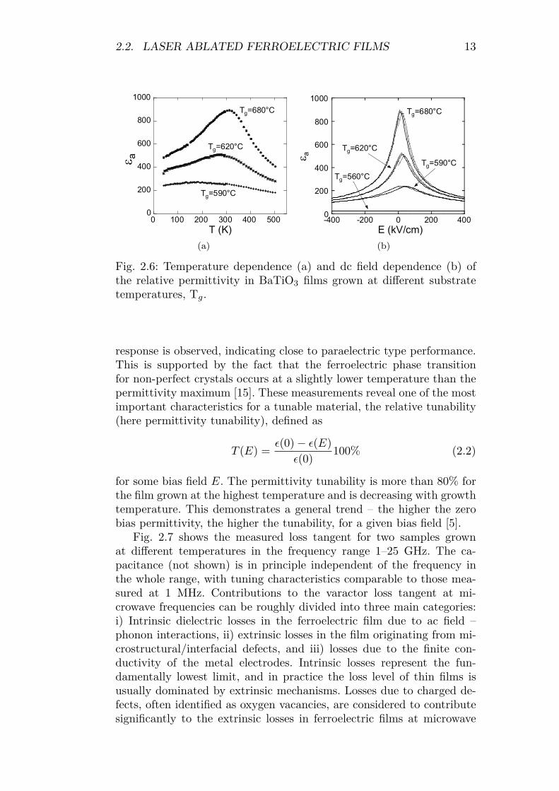
2.2. LASER ABLATED FERROELECTRIC FILMS 13
0
200
400
600
800
1000
0 100 200 300 400 500
ε a
T (K)
Tg=680°C
Tg=620°C
Tg=590°C
(a)
0
200
400
600
800
1000
-400 -200 0 200 400
ε a
E (kV/cm)
Tg=680°C
Tg=590°C
Tg=620°C
Tg=560°C
(b)
Fig. 2.6: Temperature dependence (a) and dc field dependence (b) ofthe relative permittivity in BaTiO3 films grown at different substratetemperatures, Tg.
response is observed, indicating close to paraelectric type performance.This is supported by the fact that the ferroelectric phase transitionfor non-perfect crystals occurs at a slightly lower temperature than thepermittivity maximum [15]. These measurements reveal one of the mostimportant characteristics for a tunable material, the relative tunability(here permittivity tunability), defined as
T (E) =ε(0)− ε(E)
ε(0)100% (2.2)
for some bias field E. The permittivity tunability is more than 80% forthe film grown at the highest temperature and is decreasing with growthtemperature. This demonstrates a general trend – the higher the zerobias permittivity, the higher the tunability, for a given bias field [5].
Fig. 2.7 shows the measured loss tangent for two samples grownat different temperatures in the frequency range 1–25 GHz. The ca-pacitance (not shown) is in principle independent of the frequency inthe whole range, with tuning characteristics comparable to those mea-sured at 1 MHz. Contributions to the varactor loss tangent at mi-crowave frequencies can be roughly divided into three main categories:i) Intrinsic dielectric losses in the ferroelectric film due to ac field –phonon interactions, ii) extrinsic losses in the film originating from mi-crostructural/interfacial defects, and iii) losses due to the finite con-ductivity of the metal electrodes. Intrinsic losses represent the fun-damentally lowest limit, and in practice the loss level of thin films isusually dominated by extrinsic mechanisms. Losses due to charged de-fects, often identified as oxygen vacancies, are considered to contributesignificantly to the extrinsic losses in ferroelectric films at microwave

14 CHAPTER 2. FERROELECTRIC THIN FILMS
0
0.05
0.1
0.15
0 5 10 15 20 25
tanδ
f (GHz)
20 V
10 V
0 V
Tg=590°C
(a)
0
0.05
0.1
0.15
0 5 10 15 20 25
tanδ
f (GHz)
0 V
10 V
20 V
Tg=680°C
(b)
Fig. 2.7: Loss tangent as a function of frequency, with dc bias voltageas parameter, for BaTiO3 films grown at 590◦C (a) and 680◦C (b).
frequencies [5, 16]. This loss mechanism has an approximate functionaldependence tanδch ∝ εω [5], and the results presented in Fig. 2.7 canbe seen to be in qualitative agreement with this dependence. Reducingthe permittivity of the films, either by growth temperature or by biasfield, results in a reduction in the loss tangent. Losses due to series resis-tance of electrodes would in principle reveal a similar bias dependence(∝ ωRSC(E)) but this contribution can be considered small for thetype of test structure and electrodes used for these measurements [16].An additional effect, resonant acoustic absorption of the microwave en-ergy, is the origin of the peaks in the losses observed under bias below10 GHz. The electro-acoustic properties of BSTO films will be coveredin chapter 3.
In summary the study of BaTiO3 samples prepared at different sub-strate temperatures reveal that a higher growth temperature leads tomore bulk-like properties in terms of permittivity and tunability. Thedielectric losses however decrease with bias field for all films, indicatingthat an extrinsic loss mechanism is still dominant [17].
In Paper [F] an attempt was made to explain the observed differencesin film permittivity as due to a change in the grain size with growthtemperature. The grain size (column width) distribution of each samplecould due to the known columnar structure be estimated using analysisof AFM images of the film surfaces. A clear trend was observed with amean grain diameter increasing with growth temperature from 25 nmto 35 nm over the studied interval (560◦C to 680◦C). A model assumingthe film to consist of grain cores with bulk-like properties surroundedby amorphous low permittivity grain boundary regions was successfulin describing the room temperature permittivity variations, but not theoverall permittivity behavior over a wide temperature range (shift in the

2.2. LASER ABLATED FERROELECTRIC FILMS 15
apparent Curie temperature). The commonly referred series capacitormodel, or dead layer model, assuming instead a layer of low permittivitymaterial in series with a more bulk-like part of the film, was found to beable to qualitatively explain these effects. No microstructurally distinctlayer was however observed in series with the columnar grains in thesefilms.
The series capacitor model can be used to reproduce the commonlyobserved thickness dependence of ferroelectric thin film properties, andhas been the subject of extensive research, without reaching a univer-sally accepted explanation. Several proposed mechanisms, apart from amicrostructurally distinct true dead layer, have been found to result inseries capacitance type behavior, including Schottky barrier depletionregions at the film/electrode interfaces [18], space charge within non-ideal electrodes [19], interfacial discontinuities affecting the polarizationstate [15], strain gradients [20], etc. It can be added that measurementson lamellae as thin as 75 nm, produced from single crystal BaTiO3
using focused ion beam etching, have shown bulk-like properties, indi-cating that the thickness degradation of thin films in principle can beavoided [21, 22].
2.2.2 Impact of oxygen pressure
An important growth parameter in the PLD process, apart from thesubstrate temperature, is the amount of reactive O2 gas in the chamberduring deposition. Fig. 2.8 shows the room temperature zero bias per-mittivity as a function of the O2 pressure for a series of BaTiO3 filmsgrown at 650◦C, revealing a maximum at 0.2 mbar. Changes in the filmstoichiometry is the most probable reason for this strong dependence.Several studies have shown that a proper Ba/Ti or (Ba+Sr)/Ti ratio ofthe film is critical in order to reach a high permittivity [23, 24]. Specif-ically, data of BaTiO3 film permittivity as a function of PLD pressure,qualitatively in agreement with the data in Fig. 2.8, can be found inRef. [25].
Similarly to the growth temperature studies, the films with the high-est permittivity were found to consist of the largest grains. SEM imagesof the surfaces of BaTiO3 films grown at 0.2 mbar and 0.4 mbar O2 pres-sure are shown in Fig. 2.9. The larger grains can be explained by moreenergetic plume species reaching the substrate due to fewer collisionswith gas molecules.
The film with the highest permittivity also shows higher tunability,as expected, and higher losses. Most importantly for this work howeveris that the microwave response for the film grown at 0.2 mbar O2 revealsthe most pronounced electro-acoustic effects, see Fig. 2.10. These effects,which are problematic for parallel plate varactor applications due tothe associated high loss tangent peaks, form the basis for the acousticresonators discussed in the next chapter.

16 CHAPTER 2. FERROELECTRIC THIN FILMS
400
600
800
1000
1200
0 0.1 0.2 0.3 0.4 0.5 0.6
ε a
O2 (mbar)
Fig. 2.8: Relative apparent permittivity as a function of oxygen pressureduring BaTiO3 film growth.
(a) (b)
Fig. 2.9: SEM images of BaTiO3 films grown by laser ablation at (a)0.2 mbar O2, and (b) 0.4 mbar O2.

2.2. LASER ABLATED FERROELECTRIC FILMS 17
0
0.2
0.4
0.6
0.8
0 5 10 15 20 25
tanδ
f (GHz)
0 V
20 V
Fig. 2.10: Loss tangent as a function of frequency for BaTiO3 film grownat 0.2 mbar O2.
In summary the PLD results presented in the previous sections showthat the dielectric properties of the ferroelectric film depend stronglyon the growth parameters. The highest permittivity and tunability is ob-tained at a high growth temperature and O2 pressure close to 0.2 mbar.These results were obtained using a BaTiO3 target. It should be notedhowever that most of the results are qualitatively representative also forBa0.25Sr0.75TiO3 films, which are the main focus of the following chap-ters. Similar dependencies on substrate temperature and O2 pressureduring PLD have been observed for Ba0.25Sr0.75TiO3 films during thiswork.


Chapter 3
Tunable thin film bulk
acoustic wave resonators
3.1 Introduction
Resonators are key components in a multitude of frequency generatingand frequency selective components such as oscillators and various typesof filters. Applications range from radio communication systems to wristwatches to sensors, and piezoelectric crystals have been extensively usedas the resonant element. An ac electric field applied to a piezoelectriccrystal excites acoustic waves which result in a resonance at a frequencydetermined by the mechanical properties and physical dimensions of thecrystal. Since the resonance frequency of piezoelectric resonators basedon bulk acoustic waves depend on the crystal dimensions, the upper pos-sible frequency of operation is mainly determined by the thickness ofthe piezoelectric crystal plate. For the conventional approach, cleavingof bulk material into thinner crystals, the maximum frequency is gener-ally below a few hundred MHz. Applications in e.g. wireless communi-cation systems require small size, high Q-factor resonators for frequencygeneration and filtering in the microwave frequency regime. This needhas been the driving force for the thin film bulk acoustic wave resonator(TFBAR) technology, based on piezoelectric materials in thin film form,which allows fabrication of electro-acoustic resonators operating at sev-eral GHz.
The principal TFBAR structure consists of a piezoelectric film sand-wiched between two electrodes. As an ac electric field is applied, acousticwaves are generated due to the converse piezoelectric effect and reflectedwithin the piezoelectric film. At the frequency where half the acous-tic wavelength is equal to the piezoelectric film thickness a mechanicalstanding wave is formed. The acoustic waves in turn polarize the ma-terial through the direct piezoelectric effect. For longitudinal excitationresonators like normal TFBARs, the mechanically induced polarization
19

20 CHAPTER 3. TUNABLE TFBARS
at the standing wave frequency is 180◦ out of phase with the dielectricpolarization due to the externally applied ac field. At this frequencythe net polarization charge, and thus current, is minimized, giving riseto a parallel type resonance at the electrical port. At a slightly lowerfrequency the two polarization contributions are in phase, resulting in ahigh current and a series resonance. Mechanical loading of finite thick-ness electrodes and other layers in the real resonator stack results in de-viations from this ideal case which assumes perfect boundary conditions.The resonances e.g. often occur at frequencies considerably lower thanwhat is predicted by the standing wave criterion above. The descriptionis however quite instructive and qualitatively explains the occurrence ofthe series and parallel resonances as well as their strong dependence onpiezoelectric film thickness.
Practical thin film resonator designs roughly fall into two main cat-egories depending on how the necessary acoustic isolation from thethick substrate material is provided, see Fig. 3.1. The first approachinvolves removal of material below the active resonator area, forminga free-standing membrane structure, Fig. 3.1a, either by etching of thesubstrate from the backside or by using a sacrificial layer forming anair bridge structure. Acoustically this design is close to ideal, with lowimpedance air providing a high reflection coefficient and effective con-centration of the acoustic energy to the piezoelectric film. The secondapproach is based on a multilayer acoustic mirror or Bragg reflectorstructure substituting for the free surface at the bottom, Fig. 3.1b.
A comment on terminology should be made. Often in the litera-ture membrane based resonators are referred to as TFBARs or FBARswhile reflector based resonators are distinguished as solidly mountedresonators (SMRs). In this work no such distinction is made and theterm TFBAR is applied for both types. From the authors point of viewthe term TFBAR describes the type of component quite clearly (res-onator, bulk acoustic wave, thin film technology), while implying noth-ing, except by convention, about how acoustic isolation is obtained. Ifa distinction between the two main resonator types is needed in thiswork, the terms membrane type TFBAR and solidly mounted TFBARare used.
Currently the commercialized TFBAR technology is based on AlN asthe piezoelectric active layer and both membrane and solidly mounteddesigns. AlN has been successful due to its low acoustic losses and suf-ficiently high electromechanical coupling coefficient. The breakthroughapplication was the introduction of a duplexer filter for the 1900 MHzUS-PCS band in 2001, where extremely compact TFBAR technologycould replace a bulky ceramic duplexer [26]. Today TFBAR technologyis provided by several manufacturers and widely used for filtering ap-plications in mass market applications such as mobile phones and GPShandsets [27, 28, 29, 30].
Combining the many attractive properties of these conventional TF-

3.2. DESIGN AND FABRICATION 21
(a) (b)
Fig. 3.1: Schematic of membrane type resonator (a) and solidly mountedresonator (b).
BARs with tunability, i.e. a possibility to shift the resonance frequency,would enable development of a whole new range of compact compo-nents with enhanced functionalities such as tunable filters, switches,voltage controlled oscillators, etc. Some approaches to realize TFBARtuning with the conventional materials have been reported. Resonancefrequency tunability of AlN and ZnO resonators combined with MEMSstructures as tuning elements have been reported to reach 0.39% [31]and 1.47% [32], respectively. Electrostatic tuning of the bulk acousticresonator itself by applying a dc bias directly over the piezoelectric filmis however extremely weak for these materials, with reported tunabilitiessignificantly lower than 1% [32, 33].
Ferroelectric perovskite oxides, which often reveal considerable fielddependence of physical properties, are considered as an alternative forTFBARs in order to reach wider tuning ranges. Resonators based onPb(Zr,Ti)O3 (PZT) thin films show relatively high tunabilities (>3%)[34], although the inherent hysteresis due to the polar phase of thematerial might be problematic for practical applications, see Fig. 3.2a.Polar phase material also suffers from loss contributions due to domainwall motions and oscillations [35]. In this thesis practically hysteresis-free (Fig. 3.2b) solidly mounted TFBARs based on paraelectric phaseBaxSr1−xTiO3 are presented and discussed. These resonators show inprinciple no piezoelectric activity at zero bias field as can be expectedfrom material in the paraelectric phase. Applying a bias field howeverinduces a piezoelectric effect due to breaking of the centrosymmetryof the paraelectric crystal structure, and distinct field dependent reso-nances appear. The field induced piezoelectric effect is further discussedin section 3.4.
3.2 Design and fabrication
The resonators considered in this work are implemented on high re-sistivity Si substrates as solidly mounted devices of the type shown in

22 CHAPTER 3. TUNABLE TFBARS
Bias (V)
f (G
Hz)
PZT (58/42)
fp
fs
(a)
4.1
4.12
4.14
4.16
4.18
4.2
-10 -5 0 5 10 15
f (G
Hz)
Bias (V)
fpfp
fs
fs
BST (25/75)
(b)
Fig. 3.2: Resonance frequencies as a function of bias for tunable res-onators based on (a) Pb(Zr0.58Ti0.42)O3 [34] and (b) Ba0.25Sr0.75TiO3
[this work]. Notice the pronounced hysteresis for the PZT resonator.
Fig. 3.1b. Active layers consisting of either Ba0.25Sr0.75TiO3 or BaTiO3
are deposited by laser ablation as described in section 2.2. The designfrequency, 5.25 GHz, was chosen to target future applications in the5.25 GHz U-NII band and the 5.8 GHz ISM band. Reaching this exactresonance frequency has however not been a primary goal, and the fab-ricated resonators discussed in this thesis have resonance frequencies inthe 3.7–6 GHz range. Two main versions of the tunable resonators havebeen studied, both of which are designed for on-wafer one-port reflectionmeasurements with ground-signal-ground microprobes. In Paper [E] andPaper [B] resonators consisting of circular structures of the same type asshown in Fig. 2.5 are presented. This design minimizes the fabricationcomplexity and the impact of electrode parasitics. The main drawbackof this layout is the requirement to contact the active resonator areatop electrode directly with the microprobe signal pin. This may lead toresults which are difficult to repeat and interpret due to scratching ofthe electrode and possible mechanical loading of the resonator by theprobe tip.
In Paper [D] resonators with a more complex design based on pat-terning of the bottom electrode are introduced, see Fig. 3.3. The ideabehind this design is to separate the probe tips from the active resonatorarea and to evaluate tunable resonators which are possible to incorpo-rate in a circuit application. Conducting layers below the active layerneed to be patterned to avoid unwanted capacitive coupling to the topelectrode. The active resonator area is defined by the overlap betweenthe top electrode and the bottom electrode which is capacitively coupledto the top electrode ground pads. A second thick metal layer is added toreduce losses due to series resistance of the electrodes. This thick metaldoes not reach the TFBAR active area in order to keep the mechanicalloading of the resonator low. With this design repeated contacting tothe same resonator structure is not a problem due to the thick metal

3.2. DESIGN AND FABRICATION 23
Substrate
Reflector /Bottom el.
Au
Al/Au BSTO
(a)
S
G
G Reflector / Bottom el. / BSTO / Thick top el.
BSTO / Thick top el.
Active area
(b)
Fig. 3.3: Schematic cross section (a) and top view (b) of TFBAR withpatterned bottom electrode and reflector.
electrode, facilitating e.g. temperature dependence studies, described insection 3.5.
3.2.1 Bragg reflector
Conceptually similar to an optical distributed Bragg reflector, the acous-tic reflector consists of pairs of layers with alternating high and lowacoustic impedance. The thickness of these layers are specified fromthe quarter acoustic wavelength in the material at the desired reflec-tor center frequency. The acoustic impedance contrast between the twomaterials impact on the reflectivity for a given number of pairs, andon the reflector bandwidth. The most widely used material for thelow impedance layers is SiO2 due to its low impedance, low acousticattenuation, and positive impact on resonance frequency temperaturedrift [36, 37]. (In contrast to most other materials SiO2 has a positivetemperature coefficient of the elastic constant, allowing temperaturecompensation [36, 38].) High impedance materials include W, Mo andAlN. W and Mo layers provide high impedance contrast but need to bepatterned outside the resonator active area to avoid capacitive couplingwith top metal layers, increasing the fabrication complexity.
Au/SiO2
The resonators presented in Paper [E] and Paper [D] are based on ahigh impedance contrast Au/SiO2 Bragg reflector structure providinga wide bandwidth of more than 4 GHz and requiring only two pairs toachieve high reflectivity. Au is generally not considered a suitable ma-terial for bulk acoustic wave devices due to relatively high mechanicallosses at high frequencies [39]. Technological preferences, oxidation re-sistance, and possible advantages from incorporating high conductivitymaterial in the reflector stack, effectively making the bottom electrodethicker, however motivated the use of Au for the first experiments. The

24 CHAPTER 3. TUNABLE TFBARS
(a) (b)
Fig. 3.4: SEM images of the SiO2/Au Bragg reflector. (a) Etched step inthe reflector and thin bottom electrode. (b) Cross section of the etchedstep, after deposition of BSTO active layer and top electrode.
SiO2 (280 nm) and Au (150 nm) layers were deposited in situ using reac-tive rf magnetron sputtering and dc magnetron sputtering respectively.In order to obtain sufficient adhesion thin Ti layers were sputtered inbetween each reflector layer.
To be able to use the Au containing reflector in the more complexresonator design (Fig. 3.3) the reflector layers need to be removed fromareas outside the active area. This is performed using Ar ion millingat 45◦ impact angle in order to obtain a sloped sidewall. SEM imagesof the etched reflector edge is shown in Fig. 3.4. It can be noted fromFig. 3.4b that the approximately 1 μm high step disturbs the BSTOfilm growth, resulting in a rough region along the reflector edge. Thethin top electrode needs to traverse this sloped region leading to twopossible loss mechanisms: i) increased series resistance due to the roughtopography, and ii) acoustic energy being lost due to acoustic wavesbeing launched in non-vertical directions. In addition, the approach topattern the bottom electrode in the same ion milling process as the re-flector layers results in a resonator design where the Bragg reflector doesnot extend outside the active area in the etched step region where thetop electrode comes in, leading to acoustic losses along approximately25% of the resonator perimeter where the reflector is not well defined.
HfO2/SiO2
Instead of developing the metal-containing Bragg reflector further, fo-cus was shifted towards realizing a fully non-conducting reflector stack.With a non-conducting reflector only the bottom electrode would re-quire patterning, resulting in a considerably smaller step for the activelayer and top electrode to cover. The problem with resonator perimeterleakage could also be expected to be less severe since the Bragg reflector

3.2. DESIGN AND FABRICATION 25
extends “infinitely” outside the resonator active area in all directions.HfO2 is a dielectric material with sufficiently high acoustic imped-
ance to allow fabrication of a reflector stack using a reasonable numberof layers in combination with low impedance SiO2. In Paper [B] re-sults on resonators based on an all-dielectric HfO2/SiO2 reflector arereported. The SiO2 (284 nm) and HfO2 (260 nm) layers of the threepair reflector stack is deposited in situ by reactive rf magnetron sput-tering from elemental Si and Hf targets.
The reflectivity response of a given Bragg reflector can be estimatedby considering the acoustic input impedance of the layered stack be-low the active layer by iterative use of the transmission line impedanceequation
Z = ZiZl + Zi tanh γitiZi + Zl tanh γiti
(3.1)
where Zl is the impedance loading the ith layer with impedance Zi,propagation constant γi and thickness ti. The reflectivity is then givenas
R =ZBSTO − ZREFLZBSTO + ZREFL
, (3.2)
where ZBSTO is the acoustic impedance of the BSTO active layer andand ZREFL is the input impedance of all the layers below (substrate,reflector, bottom electrode). Fig. 3.5 shows the reflection response as afunction of frequency for Bragg reflectors based on HfO2/SiO2 (3 pairs)and Au/SiO2 (2 pairs). It can be noted that the bandwidth for the Aubased reflector is slightly wider due to the higher acoustic impedancecontrast, but that the center frequency reflectivities are comparable.
3.2.2 Electrodes
The choice of top and bottom electrodes sandwiching the active layeris crucial for obtaining the desired resonator characteristics. From thepoint of view of resonatorQ-factor the electrode resistance may limit theperformance, especially at the series resonance where large currents aredrawn through the device. Alleviating this by introducing thicker elec-trodes in the acoustic path however leads to increased mechanical losses,since metals in general have higher acoustic losses than dielectrics. Itcan be shown that the Q-factor reveals a maximum as a function ofelectrode thickness due to these effects [26, 40].
The effective resonator coupling coefficient, mirroring the frequencyseparation between series and parallel resonances, is also dependent onthe choice of electrode materials. High impedance electrodes confinethe acoustic energy more effectively to the active layer, leading to ahigher coupling coefficient. For a given electrode thickness the effec-

26 CHAPTER 3. TUNABLE TFBARS
Fig. 3.5: Calculated reflectivity of HfO2/SiO2 and Au/SiO2 Bragg re-flectors including a 100 nm Pt bottom electrode.
tive resonator coupling coefficient can even exceed the intrinsic cou-pling coefficient of the piezoelectric material itself [39]. This effect hasbeen proven crucial for the success of AlN-based resonator filters sincethe effective coupling coefficient determines the separation between theseries and parallel resonances, and thus is directly connected to filterbandwidth. Mobile phone filters require effective coupling coefficients of6–7%, reached with small margin by AlN based TFBARs [41]. Too thickelectrodes lead to a reduction of the effective coupling coefficient (andtunable TFBAR tunability [42]) because a larger portion of the res-onator volume is consisting of non-piezoelectric electrode material [39].
An additional factor related to electrode thickness is the mass load-ing effect of the active layer. Thicker (and more dense) electrodes leadto a lowering of the resonance frequencies. Compensating for this massloading can be done by using a thinner active layer, which may or maynot be desirable depending on the application.
In order to maximize Q-factor and coupling coefficient it seems clearthat a low resistivity, high acoustic impedance material is preferable.High impedance electrodes commonly used for AlN TFBARs includeMb and W. If electrode resistance is an issue dual layer electrodes canbe used, with a high impedance material in contact with the active layerto maximize the coupling, covered by a second layer of a low resistivitymetal such as Al [39].
Top electrode
Throughout this work Al has been used as the main top electrode ma-terial. The advantages of Al include its low resistivity and low acousticimpedance. This allows a low electrode resistance without excessive res-
3.2. DESIGN AND FABRICATION 27
onator loading. Due to the relatively high frequency the active BSTOlayer thickness is already small, in the 200–400 nm range. This lowthickness combined with the high dielectric constant of BSTO resultsin very small resonators in order to reach reasonable impedance levels.Resonator loading should thus be kept as low as possible. No specificgoal for the resonator effective coupling coefficient has been pursuedand higher impedance top electrodes have not been considered in thiswork.
Bottom electrode
The choice of bottom electrode is more critical since it also serves asthe template on which the BSTO active layer is grown. As mentionedin section 2.2 the generally preferred material for contacting BSTO thinfilms is Pt due to its inertness and high work function. Au electrodeshave also been studied for varactor applications with promising resultsdue to its higher conductivity [43].
The resonators presented in Paper [E] and Paper [D] are based on Aubottom electrodes, deposited in situ with the Au/SiO2 Bragg reflector.
As the all-dielectric HfO2/SiO2 Bragg reflector was introduced, ef-forts were simultaneously put into developing a Pt bottom electrode.The expected benefit with Pt was the possibility to apply higher dcbias due to the superior properties of the Pt/BSTO interface. Avoid-ing the poor acoustic performance of Au was also desirable. Adhesionbetween an inert metal such as Pt and an oxide surface, here the topSiO2 layer of the reflector stack, is in general very poor. The issue iseven more pronounced since the thin Pt electrode needs to be able towithstand the high temperature BSTO film deposition with its accom-panying diffusion and thermal strain effects. Adhesion promoting layersand diffusion stop barriers need to be as thin as possible in order not todegrade the acoustic properties of the stack. Several versions of bottomelectrode configurations were studied, including Pt, Ti/Pt, TiO2/Pt,Ti/TiO2/Pt, TiO2/Au/Pt, Ti/TiN/Pt, W/Pt, using varying process-ing conditions. Several of the combinations result in very rough surfacesafter high temperature BSTO deposition, most probably due to diffu-sion of Ti leading to locally reduced adhesion and TiOx inclusions inthe Pt layer [44]. A Ti(20 nm)/TiO2(25 nm)/Pt(100 nm) electrode wassuccessfully used for the resonators presented in Paper [B]. This elec-trode is deposited by magnetron sputtering using radiative heating ofthe substrate during the deposition of the Ti/TiO2 layers, and resultsin a relatively smooth surface after BSTO deposition. The key here isthe substrate heating, oxidizing also the thin metallic Ti layer duringsubsequent reactive sputtering of TiO2. Auger electron spectroscopy ofthe Pt surface of this electrode structure after annealing in an O2 at-mosphere (BSTO deposition conditions) showed no trace of Ti. Thesame electrode structure, deposited without substrate heating, however

28 CHAPTER 3. TUNABLE TFBARS
(a) (b)
Fig. 3.6: (a) Auger electron spectroscopy data revealing presence of TiO2
on the surface of Ti/TiO2/Pt electrode after annealing in BSTO growthconditions. (b) Reference TiO2 spectrum from Ref. [45]
.
show clear evidence of TiO2 on the surface of Pt after O2 ambient an-nealing, see Fig. 3.6, indicating diffusion of Ti through the Pt film andsubsequent oxidation at the surface.
For the filter samples, described in chapter 4, a TiO2/Pt electrodewas used.
3.3 Measurement results
Wideband microwave measurements of the fabricated resonators havebeen performed using HP8510C and Agilent N5230A network analyz-ers. The resonator structures were contacted using ground-signal-groundmicroprobes for one-port reflection measurements.
3.3.1 De-embedding procedure
In order to evaluate the resonator itself, without the impact of lead stripsand contact resistance, measurements of the resonator test structuresof the type shown in Fig. 3.3 are de-embedded using dedicated on-wafer calibration structures, see Fig. 3.7. De-embedding is performed byextracting YTFBAR from the schematic of Fig. 3.7c. The main impactof this de-embedding is the removal of series inductance due to the leadstrips between the active area of the resonator and the contact pads.
Measurements of the circular test structures can be de-embeddedby subtracting the series resistance of the electrodes (and the contactresistance), found as the real part of the impedance at the high frequencylimit [46]. This gives a closer estimate of the mechanical Q-factor, i.e. anindication of the mechanical properties of the BSTO film itself.

3.3. MEASUREMENT RESULTS 29
(a) (b) (c)
Fig. 3.7: Short (a) and open (b) calibration structures used for resonatormeasurement de-embedding using the circuit (c).
3.3.2 Resonators with Au/SiO2 reflector and Aubottom electrode
Fig. 3.8 shows room temperature measurement results, presented inPaper [D], for a resonator of the type shown in Fig. 3.3 based onBa0.25Sr0.75TiO3, a Au/SiO2 Bragg reflector and Au bottom electrodes.With no dc bias applied, the response is smooth and the device behaveslike a parallel plate capacitor, as expected for BSTO in the paraelectricphase. As dc bias is applied the film becomes piezoelectrically active andthe acoustic effects appear, with resonances gradually developing andshifting towards lower frequencies with increasing bias. In agreementwith the description of the general TFBAR principle in section 3.1, aseries type resonance (minimum impedance) closely followed by a par-allel type resonance (maximum impedance), is seen at approximately4.2 GHz. A clear difference can be noted comparing the wideband fre-quency response in Fig. 3.8 with the loss tangent measurements for avaractor structure in Fig. 2.7 or Fig. 2.10. The multitude of absorptionpeaks observed in the varactor case reveals that the layered structurehas not been designed with acoustic phenomena in mind. In contrastthe TFBAR measurements show a single well defined resonance responsedue to the acoustically appropriate layer thicknesses and materials. Theelectro-acoustic effects in varactors are further discussed in Paper [C].Measurements of the basic circular resonator structures presented inPaper [E] reveal qualitatively similar results.
Fig. 3.9 shows the series and parallel resonances, fs and fp, nor-malized to the (vanishing) zero bias value, and the effective couplingcoefficient k2
t , as a function of dc bias voltage. Results for resonatorsbased on both Ba0.25Sr0.75TiO3 and BaTiO3 are included. The coupling

30 CHAPTER 3. TUNABLE TFBARS
1
10
100
3.8 4 4.2 4.4 4.6 4.8
|Z| (Ω
)
f (GHz)
1
10
100
0 10 20
|Z| (Ω
)
f (GHz)
(a)
-100
-80
-60
-40
-20
0
20
40
3.8 4 4.2 4.4 4.6 4.8
φΖ (
°)
f (GHz)
-100
-50
0
50
0 10 20
φZ (
°)
f (GHz)
(b)
Fig. 3.8: Measured magnitude (a) and phase (b) of a Ba0.25Sr0.75TiO3
resonator input impedance. Au/SiO2 Bragg reflector and Au bottomelectrode. Arrows indicate increasing dc bias voltage 0, 2, 5, 10, and15 V. Insets: 0.5–20 GHz, 15 V.
coefficient is computed as [47]
k2t =π
2
fsfp
cot
(π
2
fsfp
). (3.3)
In the Ba0.25Sr0.75TiO3 case the series resonance tunability reaches 1.7%at 15 V dc bias and the resonances are tuned towards lower frequencies,with a maximum effective coupling coefficient k2
t of 3.7%. In principle nohysteresis is visible as the bias is swept 0V→ 15V→ 0V. In the BaTiO3
case the resonances are in contrary shifted towards higher frequencieswith increasing bias, with a series resonance tunability of 1.3% and aparallel resonance tunability of 3.3%. The coupling coefficient reaches5.5% at 15 V bias and a marked hysteresis is observed. The resonatorQ-factor is estimated as [47]
Q =f
2
∣∣∣∣dφZdf∣∣∣∣f=fres
, (3.4)
where φZ is the phase of the input impedance and fres is the resonancefrequency. The Q-factor reaches a value slightly above 100 for bothresonances above 2 V bias for the Ba0.25Sr0.75TiO3 resonator. The Q-factor for the BaTiO3 TFBAR is lower, around 50 for the higher biaspoints.
3.3. MEASUREMENT RESULTS 31
0.98
0.99
1
1.01
1.02
1.03
1.04
0 5 10 15
f (n
orm
)
Bias (V)
BSTO
BTO
fs
fs
fp
fp
(a)
0
1
2
3
4
5
6
0 5 10 15
kt2
(%
)
Bias (V)
BTO
BSTO
(b)
Fig. 3.9: Series and parallel resonances (normalized) (a) and effec-tive coupling coefficient (b) as a function of dc bias voltage forBa0.25Sr0.75TiO3 and BaTiO3 resonators. Au/SiO2 Bragg reflector andAu bottom electrode.
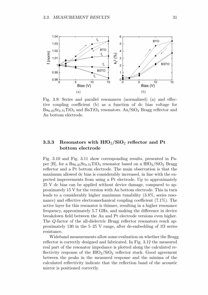
3.3.3 Resonators with HfO2/SiO2 reflector and Ptbottom electrode
Fig. 3.10 and Fig. 3.11 show corresponding results, presented in Pa-per [B], for a Ba0.25Sr0.75TiO3 resonator based on a HfO2/SiO2 Braggreflector and a Pt bottom electrode. The main observation is that themaximum allowed dc bias is considerably increased, in line with the ex-pected improvements from using a Pt electrode. Up to approximately25 V dc bias can be applied without device damage, compared to ap-proximately 15 V for the version with Au bottom electrode. This in turnleads to a considerably higher maximum tunability (3.8%, series reso-nance) and effective electromechanical coupling coefficient (7.1%). Theactive layer for this resonator is thinner, resulting in a higher resonancefrequency, approximately 5.7 GHz, and making the difference in devicebreakdown field between the Au and Pt electrode versions even higher.The Q-factor of the all-dielectric Bragg reflector resonators reach ap-proximately 130 in the 5–25 V range, after de-embedding of 1Ω seriesresistance.
Wideband measurements allow some evaluation on whether the Braggreflector is correctly designed and fabricated. In Fig. 3.12 the measuredreal part of the resonator impedance is plotted along the calculated re-flectivity response of the HfO2/SiO2 reflector stack. Good agreementbetween the peaks in the measured response and the minima of thecalculated reflectivity indicate that the reflection band of the acousticmirror is positioned correctly.

32 CHAPTER 3. TUNABLE TFBARS
(a) (b)
Fig. 3.10: Measured magnitude (a) and phase (b) of a Ba0.25Sr0.75TiO3
resonator input impedance. Arrows indicate increasing dc bias voltage0, 2, 5, 10, 15, 20, and 25 V. HfO2/SiO2 Bragg reflector and Pt bottomelectrode.
(a) (b)
Fig. 3.11: Series and parallel resonances (a) and effective coupling coeffi-cient (b) as a function of dc bias voltage for Ba0.25Sr0.75TiO3 resonator.HfO2/SiO2 Bragg reflector and Pt bottom electrode.

3.4. MODELING AND THEORY OF INDUCED PIEZOEFFECT 33
Fig. 3.12: Measured real part of resonator input impedance at 25 V dcbias (solid line) and calculated acoustic mirror reflectivity (dotted line)as a function of frequency. Arrows mark peaks associated with leakageof acoustic energy through the reflector.
3.4 Modeling and theory of induced piezoeffect
Modeling of the BSTO TFBAR characteristics is presented in Paper [D].This modeling is based on solving the basic 1D equations for a thick-ness mode piezoelectric plate resonator taking into account mechanicalloading [47]. The electrical input impedance of such a resonator is givenby
Z =1
jωC
[1− k2
t
tanφ
φZL
], (3.5)
where C is the capacitance of the parallel plate structure, k2t is the
electromechanical coupling coefficient of the active piezoelectric layer,and φ is the acoustic phase over the active layer. ZL describes the effectsof mechanical loading and is given by
ZL =(zt + zb) cos2 φ+ j sin 2φ
(zt + zb) cos 2φ+ j(ztzb + 1) sin 2φ. (3.6)
zt and zb are the acoustic impedances loading the resonator at the topand bottom interfaces, respectively, normalized to the impedance of theactive layer. The load impedances for a multilayer structure can be com-puted by repeated use of the transmission line impedance equation (3.1).
Using the above equations a complete TFBAR structure can be sim-ulated, assuming that all material properties are known. The observeddc field dependence of the tunable resonator frequency response is aresult of the field dependent properties of the BSTO film, entering theabove equations as field dependent permittivity, piezoelectric coefficient,coupling coefficient, etc. Theoretical models for this field dependence areobtained as a result of free energy expansions taking into account higherorder dielectric and mechanical coupling terms [48, 49]. A qualitative

34 CHAPTER 3. TUNABLE TFBARS
Fig. 3.13: Schematic representation of dipoles in centrosymmetric mate-rial (left), piezoelectric material (center), and originally centrosymmet-ric material under vertical dc field (right).
understanding of the appearance of a piezoeffect in paraelectric BSTOunder dc bias can be obtained by considering the electrostrictive effect.In section 1.2 electrostriction, normally not included in the standardpiezoelectric equations, was described as a field induced mechanical de-formation or strain, S, quadratic in the polarization, P :
S = QP 2, (3.7)
where Q is the electrostrictive coefficient. Writing the polarization asP = Pdc + Pac results in
S = Q(Pdc + Pac)2 = QP 2
dc + 2QPdcPac +QP 2ac. (3.8)
The factor 2QPdc can here be identified as an effective dc field depen-dent piezoelectric coefficient as seen by a low amplitude ac field, i.e. thematerial reveals a strain response linear with the low amplitude ac fieldif biased with a larger dc field. In principle the induced piezoeffect existsin all materials under dc bias, but is very weak except for certain mate-rials such as ferroelectrics due to their high permittivity giving rise toa large polarization for a given electric field. An attempt to graphicallyillustrate the induced piezoeffect is made in Fig. 3.13, where the qualita-tive similarity of the piezoelectric material and the distorted originallycentrosymmetric material under bias field is shown. Observe that forthese two cases an applied small signal electric field or mechanical in-put results in mechanical and polarization responses, respectively, whichchange with the sign of the input, i.e. a piezoelectric effect.
Formal derivations of the field induced piezoeffect in paraelectricphase BSTO aimed at explaining the resonance behavior in BSTO TF-BARs have been developed using either polarization [48] or displace-ment field [49] free energy expansions. Choosing mechanical strain andpolarization as the independent variables leads to the following set of

3.4. MODELING AND THEORY OF INDUCED PIEZOEFFECT 35
equations [48]:
k2t =h2χ2
f
cDε, (3.9)
cD = c0 −mP 2dc −
h2εb1 + εb/χf
, (3.10)
ε = εb + χf , (3.11)
h = h0 + 2qPdc, (3.12)
where h is the effective piezoelectric coefficient, χf is the field dependentferroelectric contribution to the susceptibility, cD is the elastic coeffi-cient, ε is the permittivity, εb is the background permittivity, Pdc is thedc component of the polarization, q is the electrostriction coefficient,and m is a higher order electrostriction coefficient.
Modeling of the measured results in Fig. 3.8, based on (3.9)–(3.12)and (3.1), (3.5)–(3.6), was presented in Paper [D]. This modeling in-cludes the acoustic effects of all layers in the resonator stack as wellas the dc field dependence, see Fig. 3.14. Mechanical losses were intro-duced through complex propagation constants. The agreement betweenmodeled and experimental results is in general good for bias voltages upto 10 V. The tunable TFBAR modeling presented here assumes purelylongitudinal acoustic waves and perfectly smooth interfaces between alllayers in the resonator stack. Under these conditions it is possible to re-produce the experimentally obtained TFBAR Q-factor by assuming anunexpectedly low mechanical Q-factor of the ferroelectric film. In a realdevice a number of additional loss mechanisms, not included in typicalone-dimensional modeling, may contribute significantly to the total losslevel of the resonator. Some of these loss mechanisms are discussed insection 3.6.1.
An equivalent circuit formulation based on the same piezoelectric re-lations as discussed above is referred to as the Mason model [50]. TheMason model is a three-port representation, see Fig. 3.15a, consistingof one electrical port representing the resonator electrodes, and two me-chanical ports where mechanical loads to the upper and lower parts ofthe active layer are connected. This type of 1D resonator modeling, ei-ther based on direct use of the piezoelectric equations as in Paper [D], orequivalently, implemented in a circuit simulator (Mason model), takesmaterials properties and dimensions as inputs. This makes it a usefultool for quickly evaluating the effect of changes to the design of theresonator stack. Another commonly encountered model is the modifiedButterworth-Van Dyke (MBVD) model [51], see Fig. 3.15b, consistingof six lumped elements. Cm, Lm and Rm model the acoustic propertiesof the active layer, while C0 and R0 represent the parallel plate capac-itance and dielectric losses, respectively. Ohmic losses in electrodes are

36 CHAPTER 3. TUNABLE TFBARS
1
10
100
3.8 4 4.2 4.4 4.6 4.8
|Z| (Ω
)
f (GHz)
(a)
-100
-80
-60
-40
-20
0
20
40
3.8 4 4.2 4.4 4.6 4.8
φΖ (
° )f (GHz)
(b)
Fig. 3.14: Magnitude (a) and phase (b) of the modeled (solid lines) andmeasured (dotted lines) Ba0.25Sr0.75TiO3 TFBAR input impedance. Ar-rows indicate increasing bias voltage 0, 2, 5, 10 V.
(a) (b)
Fig. 3.15: Mason model three-port representation of TFBAR (a), andlumped element MBVD model (b).
3.5. TEMPERATURE DEPENDENCE STUDIES 37
represented by Rs. The MBVD model of the TFBAR can be extractedfrom measurements and used to represent the resonator in circuit simu-lations [40, 52]. It is also widely used as a robust method for extractingthe resonator Q-factor from measurements.
3.5 Temperature dependence studies
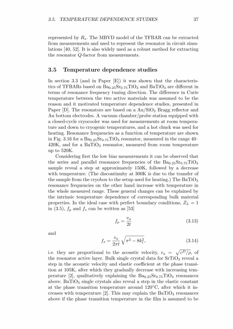
In section 3.3 (and in Paper [E]) it was shown that the characteris-tics of TFBARs based on Ba0.25Sr0.75TiO3 and BaTiO3 are different interms of resonance frequency tuning direction. The difference in Curietemperature between the two active materials was assumed to be thereason and it motivated temperature dependence studies, presented inPaper [D]. The resonators are based on a Au/SiO2 Bragg reflector andAu bottom electrodes. A vacuum chamber/probe station equipped witha closed-cycle cryocooler was used for measurements at room tempera-ture and down to cryogenic temperatures, and a hot chuck was used forheating. Resonance frequencies as a function of temperature are shownin Fig. 3.16 for a Ba0.25Sr0.75TiO3 resonator, measured in the range 40–420K, and for a BaTiO3 resonator, measured from room temperatureup to 520K.
Considering first the low bias measurements it can be observed thatthe series and parallel resonance frequencies of the Ba0.25Sr0.75TiO3
sample reveal a step at approximately 150K, followed by a decreasewith temperature. (The discontinuity at 300K is due to the transfer ofthe sample from the cryobox to the setup used for heating.) The BaTiO3
resonance frequencies on the other hand increase with temperature inthe whole measured range. These general changes can be explained bythe intrinsic temperature dependence of corresponding bulk materialproperties. In the ideal case with perfect boundary conditions, ZL = 1in (3.5), fp and fs can be written as [53]
fp =va2t
(3.13)
and
fs =va2πt
√π2− 8k2
t , (3.14)
i.e. they are proportional to the acoustic velocity, va =√cD/ρ, of
the resonator active layer. Bulk single crystal data for SrTiO3 reveal astep in the acoustic velocity and elastic coefficient at the phase transi-tion at 105K, after which they gradually decrease with increasing tem-perature [2], qualitatively explaining the Ba0.25Sr0.75TiO3 resonancesabove. BaTiO3 single crystals also reveal a step in the elastic constantat the phase transition temperature around 120◦C, after which it in-creases with temperature [2]. This may explain the BaTiO3 resonancesabove if the phase transition temperature in the film is assumed to be

38 CHAPTER 3. TUNABLE TFBARS
4.2
4.3
4.4
4.5
4.6
4.7
0 100 200 300 400
f s (
GH
z)
T (K)
BSTO
(a)
4.2
4.3
4.4
4.5
4.6
4.7
0 100 200 300 400
f p (
GH
z)
T (K)
BSTO
(b)
3.6
3.65
3.7
3.75
3.8
250 300 350 400 450 500 550
f s (
GH
z)
T (K)
BTO
(c)
3.6
3.65
3.7
3.75
3.8
250 300 350 400 450 500 550
f p (
GH
z)
T (K)
BTO
(d)
Fig. 3.16: Resonance frequencies as a function of temperature forBa0.25Sr0.75TiO3 resonator (a,b) and BaTiO3 resonator (c,d). Arrowsindicate increasing bias voltage 0, 2, 5, 10, 15 V for the Ba0.25Sr0.75TiO3
resonator and 2, 5, 10, 15 V for the BaTiO3 resonator.
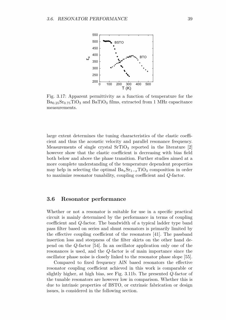
shifted close to room temperature. Low frequency measurements of thefilm permittivity, see Fig. 3.17, support this shift since the permittivitymaximum for the BaTiO3 film appears close to room temperature.
The different tuning characteristics observed for the two composi-tions are more difficult to explain fully. Considering e.g. the parallelresonance, a qualitative similarity between the Ba0.25Sr0.75TiO3 andBaTiO3 resonators can be seen in that they both tune towards higherfrequencies at low temperatures, and towards lower frequencies at hightemperatures. The tuning direction switch in the Ba0.25Sr0.75TiO3 caseroughly corresponds to the position of the presumed phase transition,while the switch for BaTiO3 occurs at a temperature much higher thanroom temperature. Using (3.10) and (3.13) this effect may in principlebe explained by a change in the sign of the parameter m, which to a
3.6. RESONATOR PERFORMANCE 39
Fig. 3.17: Apparent permittivity as a function of temperature for theBa0.25Sr0.75TiO3 and BaTiO3 films, extracted from 1 MHz capacitancemeasurements.
large extent determines the tuning characteristics of the elastic coeffi-cient and thus the acoustic velocity and parallel resonance frequency.Measurements of single crystal SrTiO3 reported in the literature [2]however show that the elastic coefficient is decreasing with bias fieldboth below and above the phase transition. Further studies aimed at amore complete understanding of the temperature dependent propertiesmay help in selecting the optimal BaxSr1−xTiO3 composition in orderto maximize resonator tunability, coupling coefficient and Q-factor.
3.6 Resonator performance
Whether or not a resonator is suitable for use in a specific practicalcircuit is mainly determined by the performance in terms of couplingcoefficient and Q-factor. The bandwidth of a typical ladder type bandpass filter based on series and shunt resonators is primarily limited bythe effective coupling coefficient of the resonators [41]. The passbandinsertion loss and steepness of the filter skirts on the other hand de-pend on the Q-factor [54]. In an oscillator application only one of theresonances is used, and the Q-factor is of main importance since theoscillator phase noise is closely linked to the resonator phase slope [55].
Compared to fixed frequency AlN based resonators the effectiveresonator coupling coefficient achieved in this work is comparable orslightly higher, at high bias, see Fig. 3.11b. The presented Q-factor ofthe tunable resonators are however low in comparison. Whether this isdue to intrinsic properties of BSTO, or extrinsic fabrication or designissues, is considered in the following section.
40 CHAPTER 3. TUNABLE TFBARS
3.6.1 Q-factor reduction mechanisms
The general definition of a resonator Q-factor involves the ratio betweenstored energy and dissipated energy per cycle. Identifying possible res-onator energy leakage paths and loss mechanisms is thus crucial in orderto increase the TFBAR Q-factor. Explaining the relatively low Q-factorof the TFBARs presented in this work is however not straight forward,and several possible limitations exist whose impact are largely unknownand difficult to estimate without specific studies.
• The intrinsic mechanical Q-factor of the BSTO material, as de-termined by its viscoelastic behaviour [53, 26], can be estimatedby extrapolation from lower frequency measurements. This re-sults in a mechanical Q-factor for SrTiO3 of approximately 1200at 5 GHz [46], indicating that fundamental viscoelastic losses arenot dominant in the resonators presented in this thesis.
• Dielectric losses in the ferroelectric film can be taken into ac-count in the TFBAR simulation (section 3.4) in analogy withvaractor modeling [7], as a conductance in parallel to the imped-ance calculated using Eq. (3.5). It is observed that high dielectriclosses mainly impact on the Q-factor at the parallel resonancefrequency. Measured dielectric loss tangents are however consid-erably lower than what would be required to reduce the resonatorQ-factor considerably.
• Ohmic losses in lead strips, contacts, and electrode plates gener-ally impact mainly on the Q-factor at the series resonance fre-quency, where the resonator impedance is very low and currentsare high [56]. The Q-factor at the parallel resonance frequency,where the impedance is high, on the other hand is only marginallyaffected by an additional resistivity contribution. Series resis-tance of the lead strips and contacts have been de-embedded ina straight-forward way for the resonators presented in this work,without affecting extracted the Q-factor considerably.
• Acoustic leakage has been quite extensively considered for AlNbased resonators, especially for the solidly mounted design, wherean acoustic leakage path into the substrate exists through the re-flector structure. Mirror layers deviating from the λ/4 thicknesswill result in energy losses for each reflection. In addition, it hasbeen shown that generation of shear waves, which are not effec-tively reflected by the mirror designed for longitudinal mode dueto lower acoustic velocity, can reduce the resonator Q-factor con-siderably [54]. Confinement of these shear waves can be improvedby a compromising optimization of the reflector layers (deviating

3.6. RESONATOR PERFORMANCE 41
(a) (b)
Fig. 3.18: Calculated reflectivity of (a) longitudinal λ/4 Bragg reflector,and (b) reflector designed to reflect both longitudinal and shear wavesat 5.25 GHz.
from the longitudinal λ/4 condition) to support reflection of bothlongitudinal and shear waves [54]. Fig. 3.18 shows calculated re-flectivities for longitudinal and shear waves for two versions ofHfO2/SiO2 reflectors. It can be clearly seen that shear wavesto a large extent leak through the reflector stack with the con-ventional design, Fig. 3.18a, while the co-optimized version re-flects both longitudinal and shear waves at the design frequency,Fig. 3.18b.
• Surface and interface roughness may be detrimental to resonatorQ-factor due to scattering of acoustic waves and possibly reso-nance broadening effects. It has been reported that the Q-factorof AlN based TFBARs is not currently limited by the effects ofsurface and interface roughness [57, 26]. From the perspectiveof tunable BSTO TFBARs two observations can be made withrespect to this claim: i) The frequency considered (∼2 GHz) islower than what has been the focus of most tunable TFBAR stud-ies (∼5 GHz). ii) The acoustic velocity of AlN (∼11000 m/s) ishigher than for BSTO (∼6000 m/s). These differences combinedresult in a considerably higher roughness to wavelength ratio inthe BSTO resonator case, and possibly much more pronouncedQ-factor reduction even at moderate roughness levels of only afew nm. In Paper [A] attempts are made to estimate the effect ofthin film roughness using two models: i) Acoustic wave attenua-tion due to roughness induced diffuse scattering, and ii) treatingthe BSTO active layer as an assembly of a large number of indi-vidual resonators acting in parallel.

42 CHAPTER 3. TUNABLE TFBARS
• Effects due to the finite lateral size of the resonators, such asgeneration of lateral modes or perimeter leakage effects due tonon-vertical components of the acoustic waves may limit the res-onator Q-factor. Due to the relatively small size of the tunableTFBARs presented in this thesis (due to the high capacitancedensity) these effects may be more pronounced than for the con-ventional AlN based TFBARs.
As shown above there are several mechanisms which may limit theQ-factor of the tunable TFBAR, perhaps in a slightly different mannerand extent than for the well developed AlN resonators. Further studiesare needed in order to increase the understanding of these mechanismsand whether they can be overcome by more careful design or fabricationoptimizations.
3.7 Conclusions
During the course of this work a few research groups have presentedresults on BaxSr1−xTiO3 TFBARs, summarized in Table 3.1. Reflectorbased as well as membrane type resonators have been reported, in thefrequency range 1.6–7 GHz. Three out of six research groups (includingChalmers) have chosen to work on a reflector based approach, while thethree other groups focus on a membrane design.
At Chalmers two different routes have been explored. The first route,the results of which are presented in this thesis, focuses on BSTOfilms grown by PLD and a resonator design based on a non-conductingBragg reflector stack for improved integration possibilities. The otherroute involves BSTO films grown by magnetron sputtering, on primar-ily W/SiO2 Bragg reflector stacks [46, 58, 59]. Some differences canbe observed when comparing the results of these two routes, see Ta-ble 3.1. The Q-factor of the magnetron sputtered resonators based onW/SiO2 reflectors are considerably higher than for the correspondingresonators presented in this work, ∼350 [46] compared to ∼130 [Pa-per [B]]. The maximum allowed dc field before device breakdown isalso higher, ∼172 V/μm [59], compared to ∼107 V/μm [Paper [B]].Despite the advantage in breakdown field, the measured effective cou-pling coefficient (and resonance tunability) for the sputtered samples islower, ∼4.4% (∼2%) [59] compared to ∼7.1% (3.8%) [Paper [B]]. If thecomparison is made at the same bias field the difference is even morepronounced. Effects of interface roughness has been identified as onepossible explanation to the difference in resonator Q-factor. In Ref. [58]TFBARs based on magnetron sputtered BSTO films on two differentBragg reflectors, W/SiO2 and HfO2/SiO2, were studied. In this studya higher Q-factor of the TFBAR based on the W/SiO2 reflector was

3.7. CONCLUSIONS 43
explained by a less pronounced surface roughness. The work presentedin Ref. [59] also suggests that roughness may be a critical issue.
From Table 3.1 it can be seen that the reported results from Chalmersare leading in terms of Q-factor [46] and coupling coefficient and tun-ability [Paper [B]]. Apart from comparisons of the actual performanceparameters, analysis of differences and trends in the various publishedresults is however difficult. The data spread is large, indicating thatindividual fabrication conditions are highly influential on the final re-sults. Factors such as active layer thickness, resonance frequency, elec-trode configuration, maximum bias field, etc. are also quite differentbetween the published results, making direct comparisons problematic.In addition possibly crucial properties such as film roughness are seldomreported.
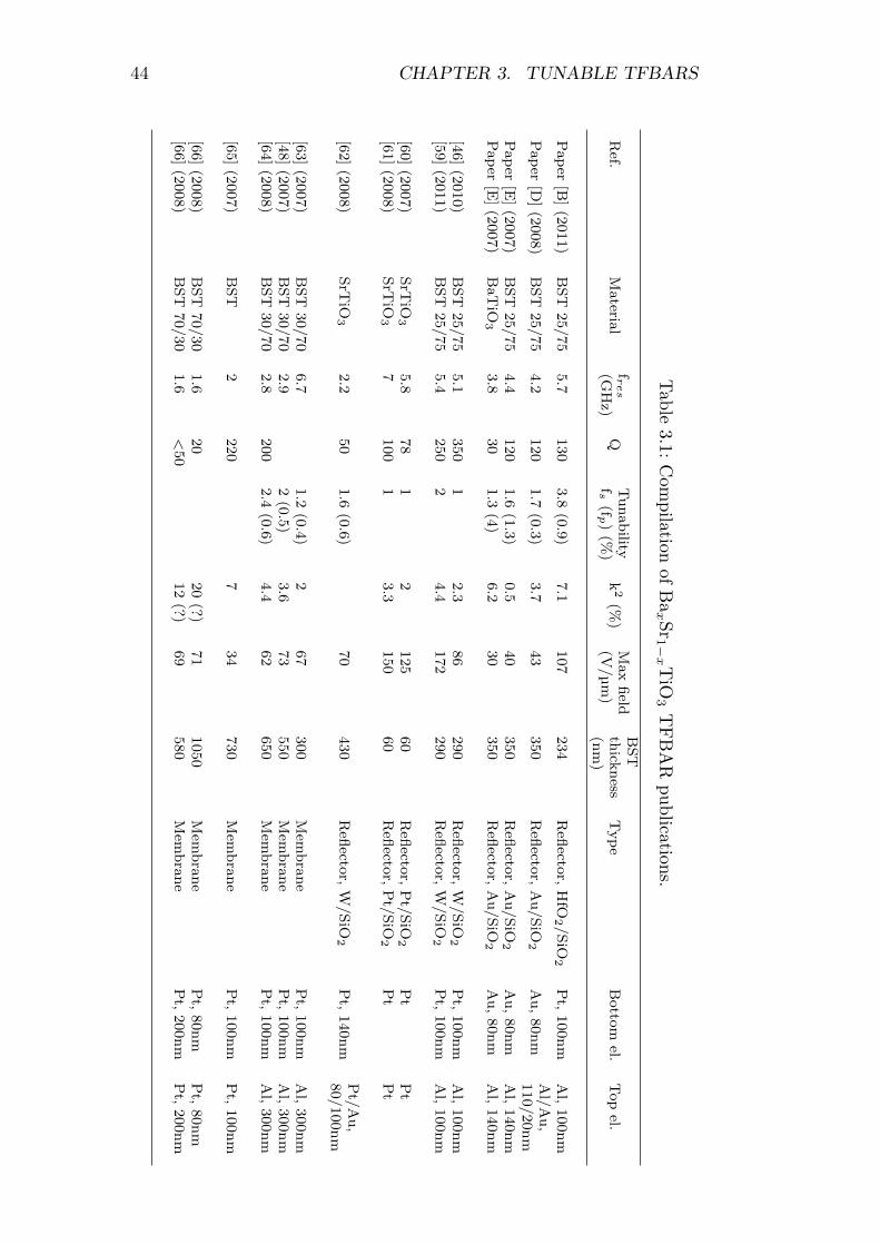
44 CHAPTER 3. TUNABLE TFBARS
Tab
le3.1:
Com
pilation
ofB
axSr1−xT
iO3
TF
BA
Rpublication
s.
Ref.
Materia
lfres
(GH
z)Q
Tu
nab
ilityfs
(fp)
(%)
k2
(%)
Max
field
(V/μ
m)
BS
Tth
ickn
ess(n
m)
Ty
pe
Botto
mel.
Top
el.
Pap
er[B
](2
011)
BS
T25/75
5.7
130
3.8
(0.9
)7.1
107
234
Refl
ector,
HfO
2/S
iO2
Pt,
100n
mA
l,100n
m
Pap
er[D
](2
008)
BS
T25/75
4.2
120
1.7
(0.3
)3.7
43
350
Refl
ector,
Au
/S
iO2
Au
,80n
mA
l/A
u,
110/20n
mP
ap
er[E
](2
007)
BS
T25/75
4.4
120
1.6
(1.3
)0.5
40
350
Refl
ector,
Au
/S
iO2
Au
,80n
mA
l,140n
mP
ap
er[E
](2
007)
BaT
iO3
3.8
30
1.3
(4)
6.2
30
350
Refl
ector,
Au
/S
iO2
Au
,80n
mA
l,140n
m
[46]
(2010)
BS
T25/75
5.1
350
12.3
86
290
Refl
ector,
W/S
iO2
Pt,
100n
mA
l,100n
m[5
9]
(2011)
BS
T25/75
5.4
250
24.4
172
290
Refl
ector,
W/S
iO2
Pt,
100n
mA
l,100n
m
[60]
(2007)
SrT
iO3
5.8
78
12
125
60
Refl
ector,
Pt/
SiO
2P
tP
t[6
1]
(2008)
SrT
iO3
7100
13.3
150
60
Refl
ector,
Pt/
SiO
2P
tP
t
[62]
(2008)
SrT
iO3
2.2
50
1.6
(0.6
)70
430
Refl
ector,
W/S
iO2
Pt,
140n
mP
t/A
u,
80/100n
m
[63]
(2007)
BS
T30/70
6.7
1.2
(0.4
)2
67
300
Mem
bra
ne
Pt,
100n
mA
l,300n
m[4
8]
(2007)
BS
T30/70
2.9
2(0
.5)
3.6
73
550
Mem
bra
ne
Pt,
100n
mA
l,300n
m[6
4]
(2008)
BS
T30/70
2.8
200
2.4
(0.6
)4.4
62
650
Mem
bra
ne
Pt,
100n
mA
l,300n
m
[65]
(2007)
BS
T2
220
734
730
Mem
bra
ne
Pt,
100n
mP
t,100n
m
[66]
(2008)
BS
T70/30
1.6
20
20
(?)
71
1050
Mem
bra
ne
Pt,
80n
mP
t,80n
m[6
6]
(2008)
BS
T70/30
1.6
<50
12
(?)
69
580
Mem
bra
ne
Pt,
200n
mP
t,200n
m
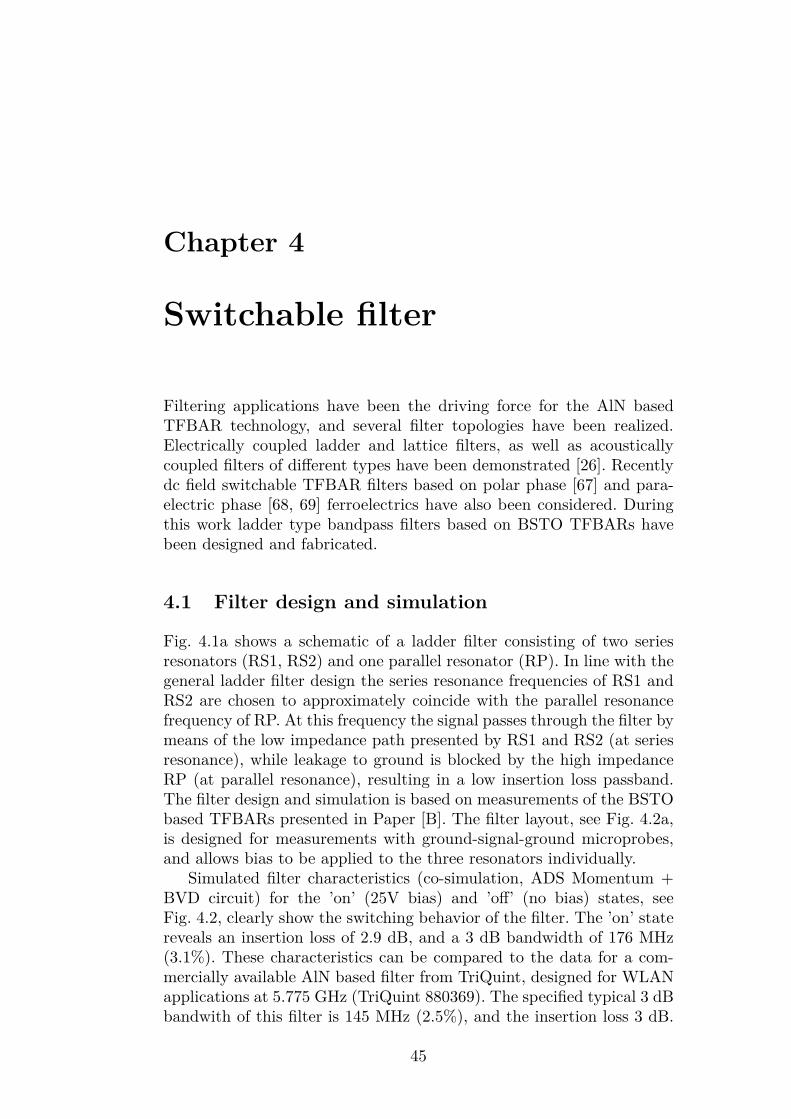
Chapter 4
Switchable filter
Filtering applications have been the driving force for the AlN basedTFBAR technology, and several filter topologies have been realized.Electrically coupled ladder and lattice filters, as well as acousticallycoupled filters of different types have been demonstrated [26]. Recentlydc field switchable TFBAR filters based on polar phase [67] and para-electric phase [68, 69] ferroelectrics have also been considered. Duringthis work ladder type bandpass filters based on BSTO TFBARs havebeen designed and fabricated.
4.1 Filter design and simulation
Fig. 4.1a shows a schematic of a ladder filter consisting of two seriesresonators (RS1, RS2) and one parallel resonator (RP). In line with thegeneral ladder filter design the series resonance frequencies of RS1 andRS2 are chosen to approximately coincide with the parallel resonancefrequency of RP. At this frequency the signal passes through the filter bymeans of the low impedance path presented by RS1 and RS2 (at seriesresonance), while leakage to ground is blocked by the high impedanceRP (at parallel resonance), resulting in a low insertion loss passband.The filter design and simulation is based on measurements of the BSTObased TFBARs presented in Paper [B]. The filter layout, see Fig. 4.2a,is designed for measurements with ground-signal-ground microprobes,and allows bias to be applied to the three resonators individually.
Simulated filter characteristics (co-simulation, ADS Momentum +BVD circuit) for the ’on’ (25V bias) and ’off’ (no bias) states, seeFig. 4.2, clearly show the switching behavior of the filter. The ’on’ statereveals an insertion loss of 2.9 dB, and a 3 dB bandwidth of 176 MHz(3.1%). These characteristics can be compared to the data for a com-mercially available AlN based filter from TriQuint, designed for WLANapplications at 5.775 GHz (TriQuint 880369). The specified typical 3 dBbandwith of this filter is 145 MHz (2.5%), and the insertion loss 3 dB.
45

46 CHAPTER 4. SWITCHABLE FILTER
(a) (b)
Fig. 4.1: Schematics of two versions of BSTO TFBAR ladder filters.
Based on this comparison the simulated performance of the switchablefilter looks very promising. The main difference is the level of out of bandrejection, which for the TriQuint filter is more than 20 dB, comparedto only 10 dB for the simulated switchable filter.
Out of band rejection can be improved by adding more sections tothe ladder circuit, at the cost of a higher in-band insertion loss. An alter-native approach is schematically shown in Fig. 4.1b where an inductorhas been added between the parallel resonator and the ground [26]. Inthe passband RP is close to parallel resonance and the inductor barelyaffects the circuit. The out of band response can however be improved ifthe inductor is chosen to series resonate with RP close to the filter cen-ter frequency. Outside the passband, where RP is capacitive, this seriesresonance results in an improved rejection. Fig. 4.3 shows one versionof a filter layout where an inductive section has been added, includingsimulated performance. As can be seen the out of band characteristicsis considerably improved. The ’off’ state rejection is also improved asa result of the LC resonance. Due to the difference in capacitance ofRP in the ’on’ (low permittivity) and ’off’ (high permittivity) states,the value of the inductance needs to be carefully chosen in order tomaximize both extinction ratio and out of band rejection.
4.2 Fabrication and measurements
Fabrication of filter structures was performed using high resistivity Siwafers covered with HfO2/SiO2 Bragg reflector layers. TiO2/Pt bottomelectrodes were deposited by magnetron sputtering and patterned usingAr ion milling. The Ba0.25Sr0.75TiO3 active layers were deposited byPLD. Al top electrodes were deposited by magnetron sputtering andpatterned using a lift-off process. Two different lithography masks forthe top electrodes enabled proper shifting of the parallel resonator reso-nance by deposition of a slightly thicker electrode. A thick Au electrodewas evaporated and patterned using lift-off.

4.2. FABRICATION AND MEASUREMENTS 47
(a)
(b)
(c)
Fig. 4.2: Filter layout (a) and simulated characteristics (b, c). Versionwithout added inductance, corresponding to the schematic in Fig. 4.1a

48 CHAPTER 4. SWITCHABLE FILTER
(a)
(b)
(c)
Fig. 4.3: Filter layout (a) and simulated characteristics (b,c). Versionwith added inductance, corresponding to the schematic in Fig. 4.1b
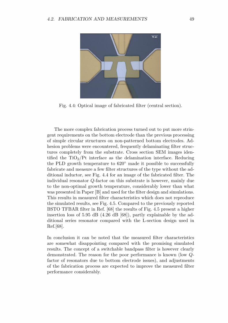
4.2. FABRICATION AND MEASUREMENTS 49
Fig. 4.4: Optical image of fabricated filter (central section).
The more complex fabrication process turned out to put more strin-gent requirements on the bottom electrode than the previous processingof simple circular structures on non-patterned bottom electrodes. Ad-hesion problems were encountered, frequently delaminating filter struc-tures completely from the substrate. Cross section SEM images iden-tified the TiO2/Pt interface as the delamination interface. Reducingthe PLD growth temperature to 620◦ made it possible to successfullyfabricate and measure a few filter structures of the type without the ad-ditional inductor, see Fig. 4.4 for an image of the fabricated filter. Theindividual resonator Q-factor on this substrate is however, mainly dueto the non-optimal growth temperature, considerably lower than whatwas presented in Paper [B] and used for the filter design and simulations.This results in measured filter characteristics which does not reproducethe simulated results, see Fig. 4.5. Compared to the previously reportedBSTO TFBAR filter in Ref. [68] the results of Fig. 4.5 present a higherinsertion loss of 5.95 dB (4.26 dB [68]), partly explainable by the ad-ditional series resonator compared with the L-section design used inRef.[68].
In conclusion it can be noted that the measured filter characteristicsare somewhat disappointing compared with the promising simulatedresults. The concept of a switchable bandpass filter is however clearlydemonstrated. The reason for the poor performance is known (low Q-factor of resonators due to bottom electrode issues), and adjustmentsof the fabrication process are expected to improve the measured filterperformance considerably.

50 CHAPTER 4. SWITCHABLE FILTER
(a)
(b)
Fig. 4.5: Measured characteristics of fabricated filter. The ’off’ state isobtained at zero bias. In the ’on’ state the resonators are biased at 15V(RS1), 15V (RS2), and 25V (RP).
Chapter 5
Summary and outlook
The main achievement of this work has been the demonstration, char-acterization, and development of a novel type of electrically switchableand tunable thin film bulk acoustic wave resonator. The resonators arebased on primarily paraelectric phase Ba0.25Sr0.75TiO3 thin films andreveal a non-hysteretic tuning response as a result of the pronouncedelectric field induced piezoelectric effect.
In terms of resonator performance the achieved effective electrome-chanical coupling coefficient at high dc bias, 7.1%, is comparable tocorresponding AlN based fixed frequency resonators. The series reso-nance frequency tunability reaches 3.8%, corresponding to an absolutetunability of approximately 200 MHz, the highest reported for non-hysteretic tunable TFBARs. The Q-factor however is considerably lowerthan what could be expected based on comparisons with fixed-frequencycounterparts. It should however be pointed out that the BSTO TFBARsshould primarily be compared to existing tunable technologies, such asresonators based on semiconductor or ferroelectric varactors. From thisperspective the already obtained Q-factor of the TFBARs is not as pooras a direct comparison with the fixed frequency AlN counterpart wouldimply. The Q-factor of ∼130 achieved in this work is already compet-itive to e.g. varactor based LC resonators, due to the limited varactorQ-factor.
Further work should be focused on understanding more thoroughlywhich loss mechanisms are dominant and which countermeasures can beapplied within resonator design and fabrication development. Studiesindicate that interface roughness of the layers in the acoustic path iscurrently limiting the Q-factor of BSTO resonators based on HfO2/SiO2
resonators [58]. It needs to be determined if roughness generating effects,such as strain, in the HfO2/SiO2 reflector can be alleviated or if analternative reflector design should be considered.
Studies aiming at understanding the observed differences in perfor-mance between resonators based on BSTO films grown by magnetron
51

52 CHAPTER 5. SUMMARY AND OUTLOOK
sputtering and PLD could give valuable information. Possibly then res-onators with a combined high effective coupling coefficient and tunabil-ity (characteristic of PLD samples on HfO2/SiO2 reflector) and a highQ-factor (characteristic of sputtered samples on W/SiO2 reflector [46])could be achieved.
Preliminary results from a switchable bandpass filter based on theBSTO TFBARs have also been presented. The filter performance islimited by the very low Q-factor of the individual resonators on themeasured filter substrate. This is a result of fabrication issues related tothe bottom electrode adhesion, which turned out to be insufficient forthe more complex filter fabrication process. Further efforts need to beput on the bottom electrode fabrication in order to obtain a more robustreflector/electrode interface. Although the demonstrated performance ofthe fabricated filter at this stage does not come close to the simulatedresults, the concept of a switchable filter is clearly demonstrated.
5.1 Summary of appended papers
Device fabrication was performed in the Nanofabrication laboratory atChalmers. Material characterization and measurements were performedat Chalmers.
Paper A, Impact of thin film roughness on the performanceof tunable bulk acoustic wave resonators
Two models are explored in order to estimate the impact of thin filmroughness on the Q-factor of Ba0.25Sr0.75TiO3 TFBARs. My contribu-tions: Model development with co-authors, writing the paper.
Paper B, Tunable bulk acoustic wave resonators based onBa0.25Sr0.75TiO3 thin films and a HfO2/SiO2 Bragg reflector
A resonator design based on a non-conducting Bragg reflector stack anda Pt bottom electrode is presented. Considerably improved resonator ef-fective coupling coefficient and tunability is achieved. My contributions:Development of Bragg reflector and bottom electrode fabrication, mea-surements, writing the paper.
Paper C, The effect of Bragg reflectors on the electro-mechanical performance of parallel-plate ferroelectriccapacitors
Pronounced losses in parallel plate BaxSr1−xTiO3 varactors under dcbias are explained by electro-acoustic activity as a result of the field in-duced piezoelectric effect. My contributions: Fabrication, measurements,writing the paper.

5.1. SUMMARY OF APPENDED PAPERS 53
Paper D, Field and temperature dependent parameters ofthe dc field induced resonances in BaxSr1−xTiO3-basedtunable thin film bulk acoustic resonators
A resonator design suitable for circuit integration is introduced. Fieldand temperature dependence of Ba0.25Sr0.75TiO3 and BaTiO3 TFBARsare studied. Room temperature measurements are modeled using 1Dtransmission line equations and theory for field induced piezoelectric ef-fect. My contributions: Development of fabrication process, SEM char-acterization, measurements, resonator modeling, writing the paper.
Paper E, Tunable solidly mounted thin film bulk acousticresonators based on BaxSr1−xTiO3 films
Tunable bulk acoustic wave resonators based on Ba0.25Sr0.75TiO3 andBaTiO3 films are reported. My contributions: Development of fabrica-tion process, SEM characterization, measurements, writing the paper.
Paper F, The effect of growth temperature on the nano-structure and dielectric response of BaTiO3 ferroelectric films
BaTiO3 films grown by PLD at different substrate temperatures arestudied using parallel-plate varactor structures. Correlations betweengrowth temperature, film properties, and microwave performance areexplored. My contributions: Fabrication, SEM and AFM characteriza-tion, measurements, model development with co-authors, writing thepaper.


Acknowledgments
I would like to thank my supervisor Prof. Spartak Gevorgian for hissupport and guidance, always with enthusiasm and optimism, duringmy years in his group.
My supervisor Andrei Vorobiev for invaluable discussions and tutoringregarding experimental work.
Martin Norling for rewarding discussions related to TFBARs, ferro-electrics, and general microwave issues.
Tomas Liljenfors and Markus Loffler for help with electron microscopystudies.
Janusz Kanski for help with AES studies.
The staff of the Nanofabrication laboratory, especially Henrik Frederik-sen for continuous support with thin film deposition systems and pro-cesses.
Past and present colleagues and friends at MEL/PEL/TML.
Thank you Maria �
This work was financially supported by the European Commission FP6project NANOSTAR and the Swedish Research Council project VR-FBAR.
55


Bibliography
[1] R. E. Newnham, V. Sundar, R. Yimnirun, J. Su, and Q. M. Zhang,“Electrostriction: Nonlinear Electromechanical Coupling in SolidDielectrics,” J. Phys. Chem. B, vol. 101, no. 48, pp. 10 141–10 150,1997.
[2] Landolt-Bornstein, New Series, vol. III/36A1, Springer-Verlag,2001.
[3] R. Waser, Ed., Nanoelectronics and Information Technology - Ad-vanced Electronic Materials and Novel Devices. Wiley-VCH, 2003.
[4] F. Jona and G. Shirane, Ferroelectric Crystals. Pergamon Press,1962.
[5] A. K. Tagantsev, V. O. Sherman, K. F. Astafiev, J. Venkatesh, andN. Setter, “Ferroelectric materials for microwave tunable applica-tions,” J. Electroceram., vol. 11, no. 1-2, pp. 5–66, 2003.
[6] G. H. Haertling, “Ferroelectric Ceramics: History and Technology,”J. Am. Ceram. Soc., vol. 82, no. 4, pp. 797–818, 1999.
[7] S. Gevorgian, A. Vorobiev, and A. Deleniv, Ferroelectrics in Mi-crowave Devices, Circuits and Systems. Springer, 2009.
[8] J. F. Scott, Ferroelectric Memories. Springer, 2000.
[9] D. Damjanovic, “Ferroelectric sensors,” IEEE Sensors J., vol. 1,no. 3, pp. 191–206, 2001.
[10] P. Muralt, “Piezoelectrics in micro and nanosystems: Solutions fora wide range of applications,” J. Nanosci. Nanotechnol., vol. 8,no. 5, pp. 2560–2567, 2008.
[11] M. Ohring, Materials science of thin films - Deposition and struc-ture. Academic press, 2002.
[12] G. W. Dietz, W. Antpohler, M. Klee, and R. Waser, “Electrodeinfluence on the charge transport through SrTiO3 thin films,” J.Appl. Phys., vol. 78, no. 10, pp. 6113–21, 1995.
57

58 BIBLIOGRAPHY
[13] T. Liljenfors, “The role of interfaces in oxide thin films,” Ph.D.dissertation, Chalmers University of Technology, 2007.
[14] A. Vorobiev, P. Rundqvist, K. Khamchane, and S. Gevorgian, “Sil-icon substrate integrated high Q-factor parallel-plate ferroelectricvaractors for microwave/millimeterwave applications,” Appl. Phys.Lett., vol. 83, no. 15, pp. 3144–3146, 2003.
[15] O. G. Vendik and S. P. Zubko, “Ferroelectric phase transition andmaximum dielectric permittivity of displacement type ferroelectrics(BaxSr1-xTiO3),” J. Appl. Phys., vol. 88, no. 9, pp. 5343–50, 2000.
[16] A. Vorobiev, P. Rundqvist, K. Khamchane, and S. Gevorgian, “Mi-crowave loss mechanisms in Ba0.25Sr0.75TiO3 thin film varactors,”J. Appl. Phys., vol. 96, no. 8, pp. 4642–4649, 2004.
[17] P. Bao, T. J. Jackson, X. Wang, and M. J. Lancaster, “Bariumstrontium titanate thin film varactors for room-temperature mi-crowave device applications,” J. Phys. D, vol. 41, no. 6, p. 063001,2008.
[18] H. C. Seong, L. B. Taek, K. C. Seok, L. K. Hoon, C. Hag-Ju,H. Horii, K. W. Don, L. S. In, and L. M. Young, “Depletion layerthickness and Schottky type carrier injection at the interface be-tween Pt electrodes and (Ba, Sr)TiO3 thin films,” J. Appl. Phys.,vol. 85, no. 1, pp. 287–95, 1999.
[19] C. T. Black and J. J. Welser, “Electric-field penetration into metals:consequences for high-dielectric-constant capacitors,” IEEE Trans.Electron Devices, vol. 46, no. 4, pp. 776–780, 1999.
[20] G. Catalan, B. Noheda, J. McAneney, L. J. Sinnamon, and J. M.Gregg, “Strain gradients in epitaxial ferroelectrics,” Phys. Rev. B,vol. 72, no. 2, pp. 20 102–1, 2005.
[21] M. M. Saad, P. Baxter, R. M. Bowman, J. M. Gregg, F. D. Mor-rison, and J. F. Scott, “Intrinsic dielectric response in ferroelectricnano-capacitors,” J. Phys.: Condens. Matter, vol. 16, no. 41, pp.451–6, 2004.
[22] L. W. Chang, M. McMillen, F. D. Morrison, J. F. Scott, and J. M.Gregg, “Size effects on thin film ferroelectrics: Experiments on iso-lated single crystal sheets,” Appl. Phys. Lett., vol. 93, no. 13, pp.132 904–1–3, 2008.
[23] S. Yamamichi, H. Yabuta, T. Sakuma, and Y. Miyasaka,“(Ba+Sr)/Ti ratio dependence of the dielectric properties for (Ba0.5Sr0.5)TiO3 thin films prepared by ion beam sputtering,” Appl.Phys. Lett., vol. 64, no. 13, pp. 1644–1646, 1994.
BIBLIOGRAPHY 59
[24] S. K. Streiffer, C. Basceri, C. B. Parker, S. E. Lash, and A. I.Kingon, “Ferroelectricity in thin films: The dielectric response offiber-textured (BaxSr1-x)Ti1+yO3+z thin films grown by chemicalvapor deposition,” J. Appl. Phys., vol. 86, no. 8, pp. 4565–4575,1999.
[25] T. Nakamura, Y. Yamanaka, A. Morimoto, and T. Shimizu, “Effectof oxygen pressure on (BaxSr1-x)TiO3 thin films by pulsed laserablation,” Jpn. J. Appl. Phys., vol. 34, no. 9 B, pp. 5150–5153,1995.
[26] e. Ken-ya Hashimoto, RF Bulk Acoustic Wave Filters for Commu-nications. Artech House, 2009.
[27] Avago Technologies, www.avagotech.com.
[28] TriQuint Semiconductor, www.tqs.com.
[29] Skyworks Solutions, Inc., www.skyworksinc.com.
[30] Epcos, www.epcos.com.
[31] W. Pan, P. Soussan, B. Nauwelaers, and H. A. C. Tilmans, “De-sign and fabrication of a surface micromachined frequency tunablefilm bulk acoustic resonator with an extended electrostatic tuningrange,” in Proc. IEEE Ultrason. Symp., 2005, pp. 1840–1843.
[32] W. Pang, H. Zhang, H. Yu, C. Y. Lee, and E. S. Kim, “Electricalfrequency tuning of film bulk acoustic resonator,” J. Microelec-tromech. Syst., vol. 16, no. 6, pp. 1303–1313, 2007.
[33] J. J. Kim, H. Zhang, W. Pang, H. Yu, and E. S. Kim, “Low phasenoise, FBAR-based voltage controlled oscillator without varactor,”in Int. Conf. Solid-State Sensors, Actuators and Microsyst. Dig.,2005, pp. 1063–1066.
[34] M. Schreiter, R. Gabl, D. Pitzer, R. Primig, and W. Wersing,“Electro-acoustic hysteresis behaviour of PZT thin film bulk acous-tic resonators,” J. Eur. Ceram. Soc., vol. 24, no. 6, pp. 1589–1592,2004.
[35] P. Muralt, J. Conde, A. Artieda, F. Martin, and M. Cantoni,“Piezoelectric materials parameters for piezoelectric thin films inGHz applications,” Int. J. Microwave Wireless Technolog., vol. 1,no. 01, pp. 19–27, 2009.
[36] K. M. Lakin, K. T. McCarron, and J. F. McDonald, “Temperaturecompensated bulk acoustic thin film resonators,” in Proc. IEEEUltrason. Symp., 2000, pp. 855–8.

60 BIBLIOGRAPHY
[37] R. Lanz, “Piezoelectric thin films for bulk acoustic wave resonatorapplications: From processing to microwave filters,” Ph.D. disser-tation, Ecole Polytechnique Federale de Lausanne, 2004.
[38] S. Ohta, K. Nakamura, A. Doi, and Y. Ishida, “Temperature char-acteristics of solidly mounted piezoelectric thin film resonators,” inProc. IEEE Ultrason. Symp., 2003, pp. 2011–2015.
[39] K. M. Lakin, J. Belsick, J. F. McDonald, and K. T. McCarron, “Im-proved bulk wave resonator coupling coefficient for wide bandwidthfilters,” in Proc. IEEE Ultrason. Symp., 2001, pp. 827–31.
[40] M. Norling, “Piezoelectric and ferroelectric device technologies formicrowave oscillators,” Ph.D. dissertation, Chalmers University ofTechnology, 2009.
[41] K. M. Lakin, “Thin film resonator technology,” IEEE Trans. Ul-trason., Ferroelect., Freq. Contr., vol. 52, no. 5, pp. 707–716, 2005.
[42] S. Gevorgian and A. Vorobiev, “Impact of the electrodes on thetunability of paraelectric BST film based FBARs,” in Proc. EuMC,2010, pp. 1210–1213.
[43] A. Vorobiev, J. Berge, and S. Gevorgian, “Thin filmBa0.25Sr0.75TiO3 varactors on Au bottom electrode for mi-crowave applications,” in Proc. EuMC, 2006, pp. 839–842.
[44] K. Sreenivas, I. Reaney, T. Maeder, N. Setter, C. Jagadish, andR. G. Elliman, “Investigation of Pt/Ti bilayer metallization on sil-icon for ferroelectric thin film integration,” J. Appl. Phys., vol. 75,no. 1, pp. 232–9, 1994.
[45] P. J. Moller, S. A. Komolov, and E. F. Lazneva, “Total currentspectroscopy study of metal oxide surfaces: II. Unoccupied elec-tronic states on TiO2(110) and SrTiO3(100) surfaces,” J. Phys.:Condens. Matter, vol. 12, no. 35, pp. 7705–7711, 2000.
[46] A. Vorobiev and S. Gevorgian, “Tunable thin film bulk acousticwave resonators with improved Q-factor,” Appl. Phys. Lett., vol. 96,no. 21, pp. 212 904–1–3, 2010.
[47] K. M. Lakin, G. R. Kline, and K. T. McCarron, “High-Q mi-crowave acoustic resonators and filters,” IEEE Trans. Microw. The-ory Tech., vol. 41, no. 12, pp. 2139–46, 1993.
[48] A. Noeth, T. Yamada, V. O. Sherman, P. Muralt, A. K. Tagantsev,and N. Setter, “Tuning of direct current bias-induced resonancesin micromachined Ba0.3Sr0.7TiO3 thin-film capacitors,” J. Appl.Phys., vol. 102, no. 11, pp. 114 110–1–7, 2007.

BIBLIOGRAPHY 61
[49] I. B. Vendik, P. A. Turalchuk, O. G. Vendik, and J. Berge, “Model-ing tunable bulk acoustic resonators based on induced piezoelectriceffect in BaTiO3 and Ba0.25Sr0.75TiO3 films,” J. Appl. Phys., vol.103, no. 1, pp. 014 107–1–6, 2008.
[50] D. A. Berlincourt, D. R. Curran, H. Jaffe, “Piezoelectric and piezo-magnetic materials and their function in transducers,” in PhysicalAcoustics, W. P. Mason, Ed., London, U.K.: Academic Press 1964,vol. 1, pt. A.
[51] I. J. D. Larson, P. D. Bradley, S. Wartenberg, and R. C. Ruby,“Modified Butterworth-Van Dyke circuit for FBAR resonators andautomated measurement system,” in Proc. IEEE Ultrason. Symp.,2000, pp. 863–8.
[52] M. Norling, J. Berge, and S. Gevorgian, “Parameter extraction fortunable TFBARs based on BaxSr1-xTiO3,” in IEEE MTT-S Int.Microw. Symp. Dig., 2009, p. 101.
[53] J. F. Rosenbaum, Bulk acoustic wave theory and devices. ArtechHouse, Boston, 1988.
[54] S. Marksteiner, J. Kaitila, G. G. Fattinger, and R. Aigner, “Opti-mization of acoustic mirrors for solidly mounted BAW resonators,”in Proc. IEEE Ultrason. Symp., 2005, pp. 329–332.
[55] B. Razavi, RF Microelectronics. Prentice Hall, 1998.
[56] R. Thalhammer, G. Fattinger, M. Handtmann, and S. Marksteiner,“Ohmic effects in BAW-resonators,” in IEEE MTT-S Int. Microw.Symp. Dig., 2006, p. 4 pp.
[57] R. Thalhammer, J. Kaitila, R. Aigner, and S. Marksteiner, “Pre-diction of BAW resonator performance using experimental and nu-merical methods,” in Proc. IEEE Ultrason. Symp., 2004, pp. 282–5.
[58] A. Vorobiev, J. Berge, S. Gevorgian, M. Loffler, and E. Olsson,“Effect of interface roughness on acoustic loss in tunable thin filmbulk acoustic wave resonators,” J. Appl. Phys., vol. 110, no. 2, pp.024 116–4, 2011.
[59] A. Vorobiev, “Correlations between microstructure and Q-factor oftunable thin film bulk acoustic wave resonators,” J. Appl. Phys.,vol. 110, no. 5, p. 054102, 2011.
[60] G. N. Saddik, D. S. Boesch, S. Stemmer, and R. A. York, “dcelectric field tunable bulk acoustic wave solidly mounted resonatorusing SrTiO3,” Appl. Phys. Lett., vol. 91, no. 4, pp. 043 501–1, 2007.

62 BIBLIOGRAPHY
[61] G. N. Saddik, D. S. Boesch, S. Stemmer, and R. A. York, “Stron-tium titanate DC electric field switchable and tunable bulk acous-tic wave solidly mounted resonator,” in IEEE MTT-S Int. Microw.Symp. Dig., 2008, pp. 1263–1266.
[62] A. Volatier, E. Defay, M. Aid, A. N’Hari, P. Ancey, and B. Dubus,“Switchable and tunable strontium titanate electrostrictive bulkacoustic wave resonator integrated with a Bragg mirror,” Appl.Phys. Lett., vol. 92, no. 3, pp. 032 906–3, 2008.
[63] A. Noeth, T. Yamada, V. O. Sherman, P. Muralt, A. K. Tagant-sev, and N. Setter, “DC bias-dependent shift of the resonance fre-quencies in BST thin film membranes,” IEEE Trans. Ultrason.,Ferroelect., Freq. Contr., vol. 54, no. 12, pp. 2487–2492, 2007.
[64] A. Noeth, T. Yamada, P. Muralt, A. K. Tagantsev, and N. Setter,“Tunable thin film bulk acoustic wave resonator based on paraelec-tric Ba0.3Sr0.7TiO3 thin film,” in Proc. Electroceramics XI, 2008.
[65] X. Zhu, J. D. Phillips, and A. Mortazawi, “A DC voltage dependantswitchable thin film bulk wave acoustic resonator using ferroelectricthin film,” in IEEE MTT-S Int. Microw. Symp. Dig., 2007, pp.671–4.
[66] B. Ivira, A. Reinhardt, E. Defay, and M. Aid, “Integration of elec-trostrictive Ba0.7Sr0.3TiO3 thin films into bulk acoustic wave res-onator for RF-frequency tuning under DC bias,” in Proc. IEEE Int.Freq. Control Symp., 2008, pp. 254–258.
[67] X. Zhu, V. Lee, J. Phillips, and A. Mortazawi, “An intrinsicallyswitchable FBAR filter based on barium titanate thin films,” IEEEMicrow. Wireless Compon. Lett., vol. 19, no. 6, pp. 359–361, 2009.
[68] G. N. Saddik and R. A. York, “An L-section DC electric fieldswitchable bulk acoustic wave solidly mounted resonator filterbased on Ba0.5Sr0.5TiO3,” in Proc. IEEE Int. Symp. Appl. Ferro-elect., 2011, pp. 1–4.
[69] G. N. Saddik and R. A. York, “Capacitively coupled dc voltageswitchable barium strontium titanate solidly mounted resonatorfilter,” in IEEE MTT-S Int. Microw. Symp. Dig., 2011, pp. 1–4.