surface structure of few layer graphene
TRANSCRIPT

Zhou, L., Fox, L., Włodek, M., Islas, L., Slastanova, A., Robles, E.,Bikondoa, O., Harniman, R., Fox, N., Cattelan, M., & Briscoe, W. H.(2018). Surface structure of few layer graphene. Carbon, 136, 255-261. https://doi.org/10.1016/j.carbon.2018.04.089
Publisher's PDF, also known as Version of recordLicense (if available):CC BYLink to published version (if available):10.1016/j.carbon.2018.04.089
Link to publication record in Explore Bristol ResearchPDF-document
This is the final published version of the article (version of record). It first appeared online via Elsevier athttps://doi.org/10.1016/j.carbon.2018.04.089 . Please refer to any applicable terms of use of the publisher.
University of Bristol - Explore Bristol ResearchGeneral rights
This document is made available in accordance with publisher policies. Please cite only thepublished version using the reference above. Full terms of use are available:http://www.bristol.ac.uk/red/research-policy/pure/user-guides/ebr-terms/
lable at ScienceDirect
Carbon 136 (2018) 255e261
Contents lists avai
Carbon
journal homepage: www.elsevier .com/locate/carbon
Surface structure of few layer graphene
Liangzhi Zhou a, Laura Fox a, b, Magdalena Włodek c, Luisa Islas a, Anna Slastanova a,Eric Robles d, Oier Bikondoa e, f, Robert Harniman a, Neil Fox a, Mattia Cattelan a,Wuge H. Briscoe a, *
a School of Chemistry, University of Bristol, Cantock's Close, Bristol, BS8 1TS, UKb Bristol Centre for Functional Nanomaterials, HH Wills Laboratory, University of Bristol, Tyndall Avenue, BS8 1TL, UKc Jerzy Haber Institute of Catalysis and Surface Chemistry, Polish Academy of Sciences, Niezapominajek 8, Polandd Household Care Analytical, Procter & Gamble Newcastle Innovation Centre Whitley Road, Longbenton, Newcastle, NE12 9TS, UKe XMaS, The UK-CRG, European Synchrotron Radiation Facility (ESRF), 6 Rue Jules Horowitz, BP 220, 38043, Grenoble CEDEX 9, Francef Department of Physics, University of Warwick, Gibbet Hill Road, Coventry, CV4 7AL, UK
a r t i c l e i n f o
Article history:Received 17 December 2017Received in revised form22 April 2018Accepted 29 April 2018Available online 2 May 2018
* Corresponding author.E-mail address: [email protected] (W.H.
https://doi.org/10.1016/j.carbon.2018.04.0890008-6223/© 2018 The Authors. Published by Elsevie
a b s t r a c t
Understanding surface structure of graphene is important for its integration into composite materials.Here, we have used synchrotron X-ray reflectivity (XRR) to study the structure of commercially availablegraphene samples (prepared via chemical vapor deposition, and marketed as graphene monolayers) onSiO2/Si at different temperatures. X-ray photoelectron spectroscopy, photoemission electron microscopyand atomic force microscopy (AFM) were employed to evaluate the composition and morphology of thegraphene layer. Our results indicate that the samples we characterized consisted of 3e4 layers of gra-phene, which should thus be more accurately described as few layer graphene (FLG). Furthermore, a“contaminant” layer, comprising polymethylmethacrylate and graphene multilayers, was found presentatop FLG. We also report tentative results on the effect of temperature on the graphene sample thickness.At 25 �C, the FLG thickness from XRR measurements was 13.0 ± 1.0 Å, in agreement with that obtainedfrom AFM (13.9 ± 0.7 Å). Upon heating to 60 �C, the FLG thickness expanded to 13.8 Å, which furtherincreased to 14.3 Å upon cooling to 25 �C. We attribute this temperature dependent thickness to the out-of-plane rippling of graphene as previously reported. These unprecedented results on the FLG surfacestructure are valuable to its potential bioanalytical applications.© 2018 The Authors. Published by Elsevier Ltd. This is an open access article under the CC BY license
(http://creativecommons.org/licenses/by/4.0/).
1. Introduction
Graphene is a one-atom thick, flat, carbon monolayer with ahexagonal carbon aromatic structure. As one of the basic carbonallotropes, it can be transformed into other carbon materials, suchas carbon nanotubes and fullerenes. Since the 1970s, studies ongrowing graphene monolayers on crystals have been carried out,and the first graphene was successfully exfoliated in 2004 byNovoselov and Geim [1]. The unique 2D electronic properties ofgraphene have since stimulated numerous studies aiming todevelop its use in applications such as supercapacitors, batteries,interconnects, transistors, phonon detectors, and sensors etc.[2].Concurrently, advances in the production and modification ofgraphene sheets have continued to stimulate interest in its
Briscoe).
r Ltd. This is an open access article
potential application in biotechnology [3]. For instance, the sur-face charging of graphene due to ion adsorption has beenexploited to monitor pH changes [4] and lipid membrane dis-ruptions [5].
One of the most promising methods for producing high qualitygraphene on an industrial scale is chemical vapor deposition (CVD),which involves depositing graphitic layers atop another crystallinesubstrate, such as SiC [6], Ni [7], and Cu [8]. A poly-methylmethacrylate (PMMA) coating is deposited atop via spincoating, and then the graphene can be transferred onto a desiredsubstrate (e.g. SiO2) after the original substrate is removed bychemical etching [9e12]. Graphene prepared by the CVD methodhas been reported to exhibit an electronic spectrum that can bedescribed by a 2D analogue of the Dirac equation, similar to that offree-standing graphene [3]. Among all the substrates, Cu attractedparticular attention. As confirmed by Raman spectroscopy, gra-phene deposited on Cu by the CVD method could yield over 93%
under the CC BY license (http://creativecommons.org/licenses/by/4.0/).

L. Zhou et al. / Carbon 136 (2018) 255e261256
coverage (with the rest consisting of 2e3 layer graphene), thanks toits weak interaction with graphene which benefits 2D crystalgrowth, thereby generating monolayer graphene on the Cu surface[13]. However, it is known that one of the issues with the trans-ferred CVD graphene is the residues of PMMA and etching agents[9e12].
Previous studies have shown that the physical properties ofgraphene materials are determined by their structure, specificallythe thickness and the defects or contaminants. For example, thethermal conductivity of graphene materials increases with thelayer number, withmonolayer, double-layer, and few layer graphene(FLG) (3e10 layers) showing different 2D electronic properties[14,15]; the transport properties in epitaxial graphene are influ-enced by its sp2 aromatic lattice structure, which is in turn affectedby its substrate and growth conditions [16,17]; and the presence ofripples and wrinkles on graphene is expected to have a negativeeffect on its electronic properties [13]. Thus, a precise determina-tion of the thickness and morphology of graphene samples underdifferent conditions is important.
Different techniques have been employed for the structuralcharacterisation of graphene and its derivatives, as listed andcompared in Table S1 in the Supporting Information (SI). Forinstance, graphene on silica was first revealed by optical micro-scopy, scanning electron microscopy (SEM), and atomic forcemicroscopy (AFM) [1]. Non-destructive techniques such as elec-tron microscopy (EM), Raman/Rayleigh scattering microscopy[10], ellipsometry [11,12], and near edge X-ray absorption spec-troscopy (NEXAS) [18,19] have been used to study the graphenestructure and/or its adsorbates. For the in-plane structural char-acterisation, scanning tunnelling microscopy (STM) and scanningtunnelling spectroscopy (STS) [8,13,16,25] have been used to im-age the graphene lattice. X-ray photoelectron spectroscopy (XPS)and Auger electron spectroscopy (AES) [6,26,27] assisted by lowenergy electron microscopy (LEEM) and photoemission electronmicroscopy (PEEM) measurements [17,25,28e30] have also beenemployed for the compositional, structural and morphologicalcharacterisation of graphene on conductive substrates. AFM [20],total internal reflection fluorescence correlation spectroscopy(ITIR-FCS) [5], and quartz crystal microbalance with dissipationmonitoring (QCM-D) [20] have been used to study lipid adsorp-tion on graphene and related systems. However, these techniqueshave a limited capacity to probe the out-of-plane structure of theadsorbed layer.
Another powerful technique is X-ray reflectivity (XRR), which iswidely used for probing buried interfaces and thin film monolayers[21], bilayers [22,23] and multilayers [24] structures. XRR has beenused to study the structure of graphene coated with other popularmaterials in electronic devices (e.g. HfO2 [25], Au [26], and per-ylenetetracarboxylic dianhydride (PTCDA) [27]), and exposed andburied interfacial structures of graphene grown on SiC [28,29],showing its potential to be used on the structural characterizationof graphene.
In this study, commercially available graphene samples on Si/SiO2 widely used in the studies of graphene applications have beenstudied using synchrotron XRR. XPS, PEEM and AFMwere also usedto provide complementary information on the composition andmorphology of the samples. Our findings are valuable to grapheneresearch and applications, and also demonstrat the suitability ofXRR as a sensitive method for characterising the graphene surfacestructure, paving the way for further investigations of biomolecularstructures on graphene using XRR.1
1 L. Zhou et al., “Evidence for air bubble formation on graphene surface in water”,in preparation.
2. Experimental methods
2.1. Materials
Graphene samples prepared by an established CVD methodwere purchased from Graphenea Inc.2 Briefly, the preparation pro-cess involves chemical vapor deposition of methane on a copper(Cu) foil to produce a graphene (mono)layer. Then a PMMA coatingis deposited atop via spin coating, before the copper foil is etchedaway. Finally, the graphene is transferred onto a 1 cm� 1 cm Siwafer with a 300 nm SiO2 top layer. Graphene produced is beingmarketed as “monolayer graphene”, and is widely used in thestudies to evaluate potential application of graphene monolayers inelectronic devices.
2.2. Experiment methods
The AFM investigation was conducted in ambient conditionsusing a MultiMode VIII microscope with a NanoScope V controller,utilizing PeakForce feedback control (Bruker, CA, USA). The canti-lever employed was SCANASYST_FLUIDþ with nominal springconstant and tip radius of 0.7 N m�1 and 2 nm respectively.
XPS and PEEM measurements of the graphene samples wereperformed at the Bristol NanoESCA facility. XPS measurements ofthe FLG were performed with an Argus spectrometer before andafter annealing at 450 �C at an ultra-high vacuum (UHV) basepressure of 4.0� 10�11mbar for 1 h. Core-level photoemissionspectra were acquired at 45� w.r.t. the sample surface, using amonochromatic Al Ka (1486.7 eV) X-ray source with a pass energyof 20 eV at room temperature and an estimate total energy reso-lution of 600meV. The relative composition of C, O, and Si can becalculated from their corresponding photoemission line intensities.
The PEEM was performed using a NanoESCA II, and the mea-surements were carried out at room temperature under the UHVcondition with a pass energy of 50 eV, a lateral resolution of150 nm, and an overall energy resolution of 140meV. The energycalibrationwas confirmed by fitting a Fermi edge of a cleanmetallicsubstrate at the same measurement condition. A He I (21.2 eV)discharge lamp was used as excitation source, and the absolutework function measurement for a particular sample area was ob-tained from electronic counting of the emitted photoelectrons [30].The work function values in the maps were obtained by fitting the600� 600 camera pixels spectra with an “error function”. The lowexcitation photon energy makes PEEM extremely surface sensitive(to 2e3 atomic surface layers), and the PEEM images were acquiredafter cleaning by annealing to show the surface morphology.
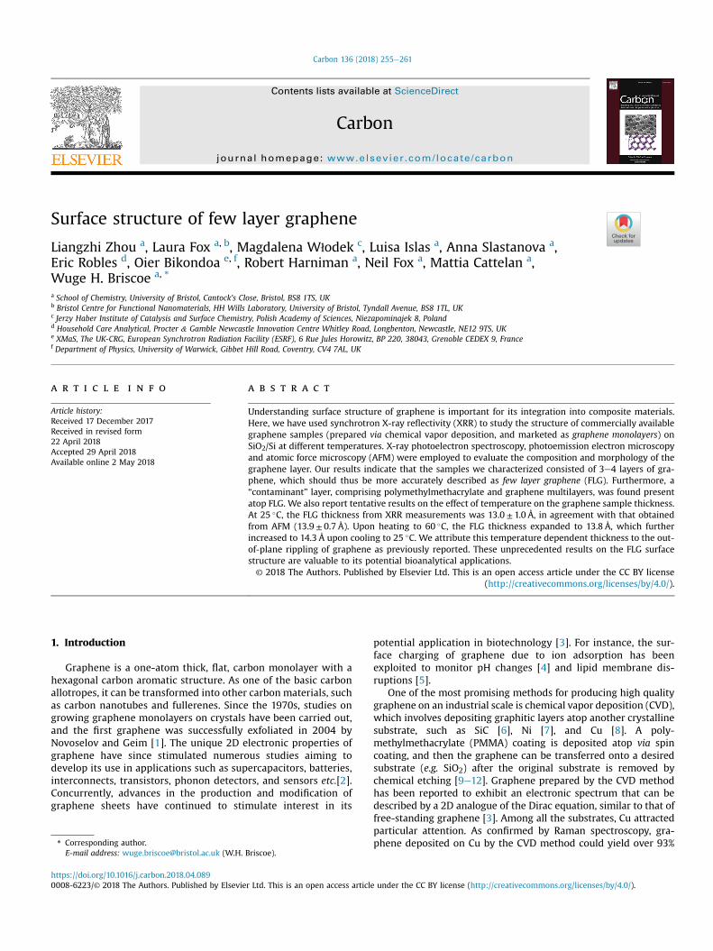
Synchrotron XRR measurements were performed at beamlineBM28-XMaS, European Synchrotron Radiation Facility (ESRF),Grenoble, France. A custom designed sample cell was used in allXRR experiments, as shown schematically in Fig. 1 [23,31]. The cell,originally designed to accommodate the “bending mica method”[21], consists of a chamber to house the sample stage for bothcurved and flat substrates. Temperature control in the range10e90 �C is facilitated by two brass jackets sandwiching thechamber, one to house electrical heaters and the other connected toa water bath to provide cooling. Graphene samples were mountedon the sample stage in the XRR cell, which was sealed via twopolyester (Mylar®) windows.
The X-ray beam energy was 14 keV (wavelength l¼ 0.8856 Å),and the incident beam size defined by aperture slits was 100 mm(vertical FWHM)� 255 mm (horizontal FWHM). XRR scans were
2 https://eu.graphenea.com/.
Fig. 1. Key components of the XRR cell, consisting of three stainless steel plates (BeD), and the cooling (A) and heating jackets (E). Two Mylar® windows (d) are clamped betweenplates B, D and plate C, creating a liquid chamber with a capacity of 5ml. Sealing is facilitated by means of O-rings placed in grooves (e). The samples (b) 1 cm� 1 cm in size areclamped by two small plates (c), onto a stainless steel stage (a). A nozzle (f) allows in situ liquid/gas exchange. The heating jacket can be controlled by two heaters (g) while thecooling jacket can be connected to a water circulating bath via an inlet (i) and an outlet (h). (A colour version of this figure can be viewed online.)
L. Zhou et al. / Carbon 136 (2018) 255e261 257
collected at 25 �C, 40 �C and 60 �C in air, with the incident angle qivarying from 0.06 to 3.0�, corresponding to a Q range of0.015e0.74Å�1, where the vertical momentum transfer vectorQ¼ 4psinq/l. The specular reflections were detected at each angle(qr¼ qi) using an Avalanche Photodiode Detector (APD). XRR datafitting was performed by using Motofit in Igor Pro (WaveMetrics,Inc., Lake Oswego, OR, USA) [32]. For reflectivity data collected on awell-defined flat substrate such as silicon, the surface layer wasmodelled as stacked homogeneous slabs. Each layer can bedescribed by three parameters: the scattering length density (SLD,r), thickness t, and inter-slab roughness Ra. These parameters werevaried in the total reflectivity calculation using the Abeles matrixmethod, and a genetic algorithm optimisation was adopted toobtain the best fitting for the curves. This generates the same resultas Parratt's Recursive method [32]. The analysis of XRR results isdescribed in the Supporting Information (SI) section SI-2.
Ellipsometry was performed using a J.A. Wollam M-2000ellipsometer (J.A. Woollam Company, Incorporated, Lincoln, NE,USA), to obtain the total thickness of the graphene sample, using awhite light source (wavelengths of 245e1000 nm) at a fixed inci-dent angle of 75�. The obtained data was processed and fitted usingVASE 32 software from J.A. Wollam adopting a three-layer model(consisting of a silicon substrate, a silicon dioxide layer and a gra-phene layer). The static contact angle of a water droplet on thegraphene sample was 76.77�±0.53� as measured using the Sessiledrop method on KRÜSS® DSA100 (see SI-5).
It is useful to compare the footprint size of different comple-mentary methods when interpreting the results. For XPS it wasapproximately an oval with major/minor axes of 3mm/2mm; forPEEM it was 60 mm� 60 mm; for XRR it was 255 mm� 1 cm (theprojection of the vertical beam size onto the sample); for ellips-ometry the circular spot size was ~3mm in diameter; for AFM, thescan size was either 5 mm� 5 mm or 1 mm� 1 mm; and for thecontact angle measurement, the diameter of the water droplet wasof ~3.3mm. As such, AFM and PEEM provided localised morpho-logical and chemical information, whilst XRR, XPS, ellipsometry,and contact angle provided average structural information across alarger sample area. It is also worth bearing in mind the differentconditions for these measurements: XPS and PEEM were carried
out under UHV (3� 10�11mbar), whilst the rest of the measure-ments were performed under ambient conditions.
3. Results and discussion
The XPS spectra from the survey scans of a wide bonding energyrange on the FLG sample before and after annealing in UHV at450 �C are shown in Fig. 2a. In both cases, only the presence of C, O,and Si was observed, and no metal residues from the originalcopper substrate and the etchant were observed on the sample. Theelemental compositions estimated from the spectra show that,before annealing, the atomic composition of C, O, and Si was 32.2%,36.7% and 31.1%, respectively; and after annealing, the percentageof C decreased to 17.4%, but those of O and Si increased to 42.6% and40.0%, respectively. The C 1s photoemission lines before and afterannealing in Fig. 2b show clear differences in their shape andrelative intensity. Deconvolution of these photoemission lines(Fig. 2c and d; Table S4) indicates the presence of C 1s (sp2 and sp3),C-OH and O-C¼O [33e35] before annealing, whereas afterannealing, the intensity of the C-OH and C¼O peaks droppedremarkedly.
The CVDmethod is known to produce graphenewith an orderedstructure and exceptional electronic properties. However, thesubstrates on which graphene can be grown are limited, and typi-cally transition metals are used. Subsequently, epitaxial grapheneoften needs to be transferred from the original growth substrate, aprocess that could cause contamination [9,10,12]. In this case, therewere four possible types of contaminants: the multilayer grapheneformed on top of the single layer graphene, the PMMA used fortransferring, residues due to incomplete Cu dissolution [11,36], andetchant liquid residues (typically FeCl3). We ascribe the observedchanges in the XPS carbon peaks in Fig. 2 to PMMA residues beingremoved by the annealing procedure. This explanation is consistentwith the observed decreased C composition (from 32.2% to 17.4%)and C/Si ratio (from 1.03 to 0.44) after annealing. Note that the XPSdetection limit was ~0.1 atomic% in our measurements.
The annealed samples were further investigated by PEEM, anextremely surface sensitive technique, to reveal their surfacemorphology, which also helps to identify any possible

Fig. 2. a) The XPS surveys for the graphene sample measured before (black line) and after (pink line) annealing. b) shows the C 1s photoemission region highlighted in the dashedrectangle in a), and the fittings for the photoemission lines before and after annealing are shown in c) and d), respectively. The fittings suggest the existence of carbon oxides in thesample, including O-C¼O and C-OH, with the peak energy values listed in Table S4 in SI-3. After annealing, the amount of the oxides decreased. e) The work function map ofgraphene annealed at 450 �C for 1 h, with 2 types of contaminants labelled as A and B. (A colour version of this figure can be viewed online.)
L. Zhou et al. / Carbon 136 (2018) 255e261258
contaminants on the graphene surface due to the contrast in theirwork function. Work function is the energy needed to excite anelectron from the Fermi level of the material to free space. Anexample work function map in Fig. 2e shows darkened (lower workfunction) lines and spots appearing on a continuous light back-ground (higher work function). We attribute the dark lines to de-fects (cracks) likely caused by the transferring process [9], and thespots to two types of contaminants (examples labelled as A and Bon Fig. 2e). Contaminants A (of size ~2 mm) were found sparselyover the sample surface, while B (of size ~500 nm) were found inthe vicinity of the defects. The work function of annealed graphene(i.e. the light background in Fig. 2e) was ~4.7e4.8 eV, which isslightly larger than the reported work function of intrinsic gra-phene (4.56 eV) [37]. This difference could be related to the redis-tribution of electrons between the substrate and graphene[7,38,39]. Upon annealing, the defects and contaminants Aremained, whereas contaminants B with a lower work function of~4.3e4.6 eV gradually disappeared. We thus attribute B to PMMAresidues from the transferring process of the graphene from its Cusubstrate during fabrication. These PMMA residues were removedupon annealing at 450 �C, an interpretation consistent with a pre-vious study which showed that PMMA was burnt off from thegraphene surface at high temperatures in UHV [11,36].
The formation of multilayer graphene with a size of fewmicrometres on monolayer graphene grown on Cu has been pre-viously characterised by Raman spectroscopy [8]. FLG with morethan 3 graphene monolayers exhibited a work function of 4.6 eV,similar to that of graphite [7,40,41]. Thus, contaminants A with awork function of ~4.6 eV were likely graphene multilayers.
Fig. 3a shows a topographic AFM image on a1 mm� 1 mm scale,and three line profiles along the coloured lines (with arrowspointing towards the directions of the profiles taken) are shown inFig. 3b shown in the corresponding colours. By analysing the to-pological histograms of the AFM images, the position and thethickness of the FLG layer can be obtained, as described in SI-4. The
highlighted areas in the line profiles represent the position of thegraphene layer from the histogram analysis, and the PMMA resi-dues with thickness in the range of 0e57 Å were seen on top of thegraphene surface. Fig. 3c shows an AFM topological image over alarger scale (5 mm� 5 mm), indicating the deposited grapheneappeared continuous with a number of defects (dark holes, i.e. 1 inFig. 3c) of size ~100 nm and a small number of PMMA residuesappearing as elevated (lighter) spots. The PMMA residues varied insize (~10e100 nm), and two such spots (2 and 3) are circled in thefigure. The red rectangle (4) in Fig. 3c highlights a crack defect onthe graphene surface with PMMA partially filling the crack. Thisinterpretation agrees with the work function map (Fig. 2e), wherePMMAwas detected around the defects. The apparent thickness ofthe graphene layer from the height histogram on a scale describedin SI-4 is 13.9± 0.7 Å, which includes any (small) spacing betweengraphene and the underlying SiO2 substrate. The graphene layerthickness points to the presence of the FLG instead of a graphenemonolayer, in agreement with numerous AFM studies determiningthe thickness of graphene and FLG on flat substrates, with the re-ported thickness ranging from 3.5 Å to 15 Å, depending on thefabrication method and the AFM imaging [1,42e44].
Assuming PMMA residues existed mostly atop the measuredsample, from the height histogram analysis, the graphene coverageon SiO2 was fg 85.1± 2.1%, as described in SI-4. However, if thegraphene did not remain intact during the transferring process,PMMA could have been transferred onto silica instead of graphene;in that case, the graphene coverage would have been over-estimated, whilst that of PMMA underestimated.
The XRR curves of the graphene samples are shown in Fig. 4b.These curves were collected at 25 �C, 40 �C and 60 �C, and after thesample was cooled back down to 25 �C after heating. It is inter-esting to study such a temperature effect, given its relevance topotential biomedical applications of graphene. These results arerepresentative from two separate synchrotron experiments on twodifferent batches of samples from the same supplier. The open

Fig. 3. a) An example AFM scale topological image on a 1 mm� 1 mm scale; b) Three line profiles followed the direction of the coloured arrow lines in a), with the grey highlightedareas attributed to the graphene layer; c) An example AFM topographic image on a 5 mm� 5 mm scale, highlighting PMMA residues (e.g. 2, 3) on a continuous graphene layer withholes (e.g. 1) and defects (e.g. 4) exposing underlying SiO2; d) the corresponding histogram shows the height distribution of SiO2, graphene, and the contaminant layer. (A colourversion of this figure can be viewed online.)
Fig. 4. a) The fitted SLD profile of the graphene sample at different temperatures with the corresponding physical model used for the fitting. Here, tc and tg are the thickness of the 2slabs representing the contaminants and graphene, respectively. b) The open circles and solid lines are corresponded to the collected XRR data points and fits on a log scale ofgraphene plotted against Q at different temperatures (with the curves offset vertically for clarity). The fitting parameters are listed in Table 1. (A colour version of this figure can beviewed online.)
L. Zhou et al. / Carbon 136 (2018) 255e261 259
circles are the experimental data points, and the solid red lines thefits using a three-layer model, with the details of XRR analysis givenin SI-2. The morphology and thickness measurement of graphenefrom AFM imaging (cf. Fig. 3) indicates that the graphene samplewas not a graphene monolayer, but more likely FLG. PEEM (cf.Fig. 2) suggests that a “contaminant” layer was present atop thegraphene layer, which was likely a mixture of graphene multilayers
and PMMA residues. Therefore, when analysing the XRR data, wehave used a three layer model (Fig. 4a): a contaminant layer (ofthickness tc) atop a graphene layer (tg) attached to the substratewith a SiO2 layer (ts). The fitted thickness (t), inter-layer roughness(Ra) and SLD (r) are listed in Table 1. Overall, the structural infor-mation from fitting the XRR data is consistent with the observa-tions from AFM and PEEM measurements.

Table 1Fitting parameters for XRR results of graphene in air at different temperatures, using the three-layer model (cf. Fig. 4a). The SLD (r) of graphene and SiO2 were fixed duringfitting, and that of the contaminant layer was fitted in the range between air to graphene, since it is presumed a layer of a mixture with limited coverage instead of a ho-mogeneous film. Also listed are the two fitted interfacial roughness values, Ra,c for the roughness at the interface between air and the “contaminant” layer (thus the subscript c)and Ra,g for that at the interface between the “contaminant” layer and the graphene layer.
T (�C) tg (Å) Ra,g (Å) r (10�6 Å�2) fg (%) tc (Å) Ra,c (Å) r (10�6 Å�2) c2 (10�3)
25 12.9 0.9 12.91 70.9 11.8 1.2 9.80 1.2140 13.4 1.0 13.06 71.8 11.6 1.1 9.90 1.8560 13.8 1.3 13.13 72.2 11.8 0.9 9.47 4.5725 (Cooled) 14.3 1.3 13.08 71.9 11.7 0.7 9.19 9.72
L. Zhou et al. / Carbon 136 (2018) 255e261260
The average fitted XRR thickness of four different graphenesamples from two different sample batches at 25 �C wastg¼ 13.0± 1.0 Å (Table S3), slightly smaller than the AFM thicknessof 13.9± 0.7 Å (Fig. 3d), which nonetheless is broadly consistentwith the conclusion that the graphene layer was FLG with anaverage of 3e4 graphene monolayers. This is probably due to XRRmeasurements giving an average thickness over a much largerfootprint (~106 mm2), while AFM measures the local apparentthickness (with a footprint of ~1 mm2) that is affected by theinteraction between the tip and the surface. The total thickness ofgraphene and the contaminant layers from XRR fitting was ~25 Å,close to the thickness (27.1± 0.8 Å) obtained from the ellipsometrymeasurement on the same graphene samples.
The coverage of each layer can be calculated by comparing thefitted r with theoretical values, i.e. f¼ rfitted/rcalculated. The fitted r
values of each layer are shown in, the theoretical r of each materialis listed in Table S2; the calculated SLD for graphene isrg¼ 1.820� 10�5 Å�2 at 14 keV. The graphene coverage at roomtemperature from XRR is fg¼ 76.3± 7.0%, broadly consistent withthe value fg ~85.1± 2.1% estimated from AFM imaging, with thediscrepancy again ascribable to the differences in the footprint sizethe two techniques probe. As such, the XRR fg value is an averageover a much larger sample area, compared to the localised infor-mation from AFM imaging.
An interesting observation is that the graphene layer thicknesstg experienced a subtle expansion from 12.9 Å at 25 �C to 13.8 Å at60 �C, and the roughness Ra,g from 0.9 Å to 1.3 Å correspondingly.Meanwhile, the thickness of the contaminant layer remainedlargely constant at tc¼ 11.7 Å, but its roughness Ra,c decreased from1.2 Å to 0.9 Å from 25 �C to 60 �C, suggesting a possible “curing”procedure upon heating, leading to a reduction of the roughness.The Ra,c value continued to decrease to 0.7 Å, suggesting possiblefurther relaxation. Furthermore, this change in the graphene layerthickness was irreversible; since after cooling to 25 �C, tg furtherincreased slightly to 14.3 Å. This observation might be explained bythe out-of-plane motion of graphene, which may also be consid-ered as a perpendicular thermal expansion or enhanced surfaceripples. Unlike most of other materials, including SiO2 and PMMA,graphene was demonstrated both theoretically and experimentallyto have a negative in-plane thermal expansion coefficient (TEC)below ~500 K, as a consequence of decreasing phonon energiesexhibited by 2D materials with smaller lattice parameters (rippled)upon heating, in contrast to increasing phonon energies in bulkmaterials [45e47]. In addition, the asymmetric bond length dis-tribution of graphene caused by the delocalized p-cloud and thestructural defects forces graphene to become non-planar to mini-mize free energy [48]. The rippling of graphene supported by Si/SiO2 upon heating above 200 K was observed with SEM [49] andRaman spectroscopy [47]. When graphene attached to a SiO2 sub-strate is heated, the graphene layer would experience an in-planecompressive stress because of its negative TEC, while SiO2 wouldhave experienced a tensile stress. Once the force applied on gra-phene exceeds the vdW attractive force between graphene and thesubstrate (normally at higher temperature), graphenemight escape
from the underling layer to enhance the amplitude of the ripples.This is also consistent with our observation that, after cooling backto room temperature, the graphene layer thickness detected by XRRfurther increased. This could be attributed to the tension on thegraphene being smaller than the pining force, and the graphenestayed attached to the substrate, manifesting in enhanced rippling.We should acknowledge that our conclusions on the temperaturedependence of the graphene sample thickness are tentative at thisstage, and more measurements are needed to further verify theseinteresting and important observations.
4. Concluding remarks
The physical properties of graphene are intimately dependenton its thickness and surface structure. Understanding the surfacestructure of graphene is also important to its integration in com-posite materials and its bioanalytic applications. In this study, XRRwas used to study the thickness of commercially sourced grapheneprepared using the CVD method on Si/SiO2 in air at different tem-peratures for the first time. Such graphene samples have beenwidely used in research and applications on monolayer graphene.Complementary techniques as AFM, XPS, and PEEM have been usedto provide information on topography and chemical compositionsof the graphene layer. Our XRR and AFM results show that thethickness of the graphene layer was ~13.0± 1.0 Å and 13.9± 0.7 Å,respectively, corresponding to 3e4 graphene monolayers. As such,the samples we characterized appeared to consist of 3e4 mono-layers of graphene. This may suggest that other such commercialgraphene samples are not of monolayer character. Given that XRRhas not been previously widely used for studying the graphenestructure, we hope to stimulate further investigations rather thanregarding our conclusions as certainty and applicable to all com-mercial graphene samples. The XPS and PEEM results suggest thepresence of PMMA residues from the transfer process of graphenefabrication. In addition, isolated islands of multilayer graphenewere also present atop the FLG layer. We also observed a slight butdetectable increase of 0.5e0.9 Å in the graphene layer thickness asit was heated from room temperature to 60 �C. This thermalexpansionwas irreversible, with the graphene thickness increasinga further 0.5 Å upon cooling back to room temperature. Suchtemperature dependent graphene thickness could be attributed tothe out of plane rippling behaviour of graphene upon heating aspreviously reported. We should acknowledge that our conclusionson the temperature dependence of the graphene sample thicknessare tentative at this stage, and more measurements are needed tofurther verify these interesting and important observations. Theseresults on the FLG surface structure and chemistry are valuable toits potential bioanalytical applications where its interactions withbiomolecules are an important consideration.
Acknowledgement
We acknowledge funding from the Engineering and PhysicalScience Research Council (EPSRC EP/H034862/1, and EP/L016648/1

L. Zhou et al. / Carbon 136 (2018) 255e261 261
through the Bristol Centre for Functional Nanomaterials (BCFN)), theRoyal Society, Taiho Kogyo Tribology Research Foundation, theEuropean Cooperation in Science and Technology (CMST COST)Action CM1101, the Marie Curie Initial Training Network (MC-ITN)“Soft, Small, and Smart: Design, Assembly, and Dynamics of NovelNanoparticles for Novel Industrial Applications (NanoS3)” (FP7 GrantNo. 290251), and the Consejo Nacional de Ciencia y Tecnologia(CONACyT) Postdoctoral Fellowship 291231. We also thank Procter& Gamble for financial support via the Bristol Final Year IndustrialProject Scheme. Synchrotron X-ray access at EPSRC funded ESRFCRG XMas beamline and the support by the beamline staff isacknowledged. The authors acknowledge the Bristol NanoESCAFacility EPSRC Strategic Equipment Grant EP/M000605/1.
Appendix A. Supplementary data
Supplementary data related to this article can be found athttps://doi.org/10.1016/j.carbon.2018.04.089.
References
[1] K.S. Novoselov, A.K. Geim, S.V. Morozov, D. Jiang, Y. Zhang, S.V. Dubonos, et al.,Electric field effect in atomically thin carbon films, Science 306 (5696) (2004)666e669.
[2] K.S. Novoselov, V.I. Fal'ko, L. Colombo, P.R. Gellert, M.G. Schwab, K. Kim,A roadmap for graphene, Nature 490 (7419) (2012) 192e200.
[3] A.K. Geim, Graphene: status and prospects, Science 324 (5934) (2009)1530e1534.
[4] P.K. Ang, W. Chen, A.T.S. Wee, K.P. Loh, Solution-gated epitaxial graphene aspH sensor, J. Am. Chem. Soc. 130 (44) (2008) 14392. -þ.
[5] P.K. Ang, M. Jaiswal, C. Lim, Y. Wang, J. Sankaran, A. Li, et al., A bioelectronicplatform using a graphene-lipid bilayer interface, ACS Nano 4 (12) (2010)7387e7394.
[6] D.C. Wang, Y.M. Zhang, Spectroscopic and scanning probe analysis on large-area epitaxial graphene grown under pressure of 4 mbar on 4H-SiC (0001)substratesl, Chin. Phys. B 23 (7) (2014) 6.
[7] R. Kadowaki, M. Kuriyama, T. Abukawa, K. Sagisaka, D. Fujita, PEEM and microPES study of graphene growth on Ni(110) substrate, E-Journal of SurfaceScience and Nanotechnology 13 (2015) 347e351.
[8] W. Liu, H. Li, C. Xu, Y. Khatami, K. Banerjee, Synthesis of high-quality mono-layer and bilayer graphene on copper using chemical vapor deposition, Car-bon 49 (13) (2011) 4122e4130.
[9] X.S. Li, Y.W. Zhu, W.W. Cai, M. Borysiak, B.Y. Han, D. Chen, et al., Transfer oflarge-area graphene films for high-performance transparent conductiveelectrodes, Nano Lett. 9 (12) (2009) 4359e4363.
[10] S. Unarunotai, Y. Murata, C.E. Chialvo, H.S. Kim, S. MacLaren, N. Mason, et al.,Transfer of graphene layers grown on SiC wafers to other substrates and theirintegration into field effect transistors, Appl. Phys. Lett. (20) (2009) 95.
[11] J.W. Suk, A. Kitt, C.W. Magnuson, Y.F. Hao, S. Ahmed, J.H. An, et al., Transfer ofCVD-grown monolayer graphene onto arbitrary substrates, ACS Nano 5 (9)(2011) 6916e6924.
[12] J.D. Caldwell, T.J. Anderson, J.C. Culbertson, G.G. Jernigan, K.D. Hobart, F.J. Kub,et al., Technique for the dry transfer of epitaxial graphene onto arbitrarysubstrates, ACS Nano 4 (2) (2010) 1108e1114.
[13] C. Mattevi, H. Kim, M. Chhowalla, A review of chemical vapour deposition ofgraphene on copper, J. Mater. Chem. 21 (10) (2011) 3324e3334.
[14] M.S. Xu, D. Fujita, J.H. Gao, N. Hanagata, Auger electron spectroscopy: arational method for determining thickness of graphene films, ACS Nano 4 (5)(2010) 2937e2945.
[15] W.Y. Jang, Z. Chen, W.Z. Bao, C.N. Lau, C. Dames, Thickness-dependent thermalconductivity of encased graphene and ultrathin graphite, Nano Lett. 10 (10)(2010) 3909e3913.
[16] G.M. Rutter, J.N. Crain, N.P. Guisinger, T. Li, P.N. First, J.A. Stroscio, Scatteringand interference in epitaxial graphene, Science 317 (5835) (2007) 219e222.
[17] Z.H. Aitken, R. Huang, Effects of mismatch strain and substrate surfacecorrugation on morphology of supported monolayer graphene, J. Appl. Phys.107 (12) (2010) 10.
[18] D.S. Geng, S.L. Yang, Y. Zhang, J.L. Yang, J. Liu, R.Y. Li, et al., Nitrogen dopingeffects on the structure of graphene, Appl. Surf. Sci. 257 (21) (2011)9193e9198.
[19] J.Q. Xu, P. Kruger, C.R. Natoli, K. Hayakawa, Z.Y. Wu, K. Hatada, X-ray ab-sorption spectra of graphene and graphene oxide by full-potential multiplescattering calculations with self-consistent charge density, Phys. Rev. B 92(12) (2015).
[20] R. Frost, G.E. Jonsson, D. Chakarov, S. Svedhem, B. Kasemo, Graphene oxideand lipid membranes: interactions and nanocomposite structures, Nano Lett.12 (7) (2012) 3356e3362.
[21] W.H. Briscoe, M. Chen, I.E. Dunlop, J. Klein, J. Penfold, R.M.J. Jacobs, Applying
grazing incidence X-ray reflectometry (XRR) to characterising nanofilms onmica, J. Colloid Interface Sci. 306 (2) (2007) 459e463.
[22] R.P. Giri, A. Chakrabarti, M.K. Mukhopadhyay, Cholesterol-induced structuralchanges in saturated phospholipid model membranes revealed through X-rayscattering technique, J. Phys. Chem. B 121 (16) (2017) 4081e4090.
[23] F. Speranza, G.A. Pilkington, T.G. Dane, P.T. Cresswell, P.X. Li, R.M.J. Jacobs, etal., Quiescent bilayers at the mica-water interface, Soft Matter 9 (29) (2013)7028e7041.
[24] B. Sironi, T. Snow, C. Redeker, A. Slastanova, O. Bikondoa, T. Arnold, et al.,Structure of lipid multilayers via drop casting of aqueous liposome disper-sions, Soft Matter 12 (17) (2016) 3877e3887.
[25] S.J. Jeong, Y. Gu, J. Heo, J. Yang, C.S. Lee, M.H. Lee, et al., Thickness scaling ofatomic-layer-deposited HfO2 films and their application to wafer-scale gra-phene tunnelling transistors, Sci. Rep. 6 (2016).
[26] M. Kalbac, V. Vales, J. Vejpravova, The effect of a thin gold layer on graphene: aRaman spectroscopy study, RSC Adv. 4 (105) (2014) 60929e60935.
[27] J.D. Emery, Q.H. Wang, M. Zarrouati, P. Fenter, M.C. Hersam, M.J. Bedzyk,Structural analysis of PTCDA monolayers on epitaxial graphene with ultra-high vacuum scanning tunneling microscopy and high-resolution X-rayreflectivity, Surf. Sci. 605 (17e18) (2011) 1685e1693.
[28] M. Conrad, J. Rault, Y. Utsumi, Y. Garreau, A. Vlad, A. Coati, et al., Structure andevolution of semiconducting buffer graphene grown on SiC(0001), Phys. Rev.B 96 (19) (2017).
[29] J.D. Emery, V.D. Wheeler, J.E. Johns, M.E. McBriarty, B. Detlefs, M.C. Hersam, etal., Structural consequences of hydrogen intercalation of epitaxial grapheneon SiC(0001) (vol. 105, 161602, 2014), Appl. Phys. Lett. 107 (18) (2015).
[30] W.Y. Li, K. Goto, R. Shimizu, PEEM is a suitable tool for absolute work functionmeasurements, Surf. Interface Anal. 37 (2) (2005) 244e247.
[31] W.H. Briscoe, F. Speranza, P.X. Li, O. Konovalov, L. Bouchenoire, J. van Stam, etal., Synchrotron XRR study of soft nanofilms at the mica-water interface, SoftMatter 8 (18) (2012) 5055e5068.
[32] A. Nelson, Co-refinement of multiple-contrast neutron/X-ray reflectivity datausing MOTOFIT, J. Appl. Crystallogr. 39 (2006) 273e276.
[33] S. Stankovich, D.A. Dikin, R.D. Piner, K.A. Kohlhaas, A. Kleinhammes, Y. Jia, etal., Synthesis of graphene-based nanosheets via chemical reduction of exfo-liated graphite oxide, Carbon 45 (7) (2007) 1558e1565.
[34] B. Lesiak, L. Stobinski, A. Malolepszy, M. Mazurkiewicz, L. Kover, J. Toth,Preparation of graphene oxide and characterisation using electron spectros-copy, J. Electron. Spectrosc. Relat. Phenom. 193 (2014) 92e99.
[35] L. Stobinski, B. Lesiak, A. Malolepszy, M. Mazurkiewicz, B. Mierzwa, J. Zemek,et al., Graphene oxide and reduced graphene oxide studied by the XRD, TEMand electron spectroscopy methods, J. Electron. Spectrosc. Relat. Phenom. 195(2014) 145e154.
[36] Y.C. Lin, C.C. Lu, C.H. Yeh, C.H. Jin, K. Suenaga, P.W. Chiu, Graphene annealing:how clean can it Be? Nano Lett. 12 (1) (2012) 414e419.
[37] R.S. Yan, Q. Zhang, W. Li, I. Calizo, T. Shen, C.A. Richter, et al., Determination ofgraphene work function and graphene-insulator-semiconductor band align-ment by internal photoemission spectroscopy, Appl. Phys. Lett. 101 (2) (2012).
[38] C.S.A. Fang, C.E. Maloney, The effect of substrate work function on workfunction reduction of Re/W alloy-coated impregnated cathodes, Appl. Phys.Mater. Sci. Process 50 (6) (1990) 603e607.
[39] M.T. Greiner, M.G. Helander, W.M. Tang, Z.B. Wang, J. Qiu, Z.H. Lu, Universalenergy-level alignment of molecules on metal oxides, Nat. Mater. 11 (1)(2012) 76e81.
[40] H. Hibino, H. Kageshima, M. Kotsugi, F. Maeda, F.Z. Guo, Y. Watanabe,Dependence of electronic properties of epitaxial few-layer graphene on thenumber of layers investigated by photoelectron emission microscopy, Phys.Rev. B (12) (2009) 79.
[41] S.S. Datta, D.R. Strachan, E.J. Mele, A.T.C. Johnson, Surface potentials and layercharge distributions in few-layer graphene films, Nano Lett. 9 (1) (2009)7e11.
[42] P. Nemes-Incze, Z. Osvath, K. Kamaras, L.P. Biro, Anomalies in thicknessmeasurements of graphene and few layer graphite crystals by tapping modeatomic force microscopy, Carbon 46 (11) (2008) 1435e1442.
[43] A.N. Sidorov, M.M. Yazdanpanah, R. Jalilian, P.J. Ouseph, R.W. Cohn,G.U. Sumanasekera, Electrostatic deposition of graphene, Nanotechnology 18(13) (2007).
[44] Z.H. Chen, Y.M. Lin, M.J. Rooks, P. Avouris, Graphene nano-ribbon electronics,Phys. E Low-dimens. Syst. Nanostruct. 40 (2) (2007) 228e232.
[45] P.K. Schelling, R. Keblinski, Thermal expansion of carbon structures, Phys. Rev.B (3) (2003) 68.
[46] M.Z. Islam, M. Mahboob, R.L. Lowe, Characterization of the thermal expansionproperties of graphene using molecular dynamics simulations (vol. 46,435302, 2013), J. Phys. Appl. Phys. 47 (40) (2014).
[47] D. Yoon, Y.W. Son, H. Cheong, Negative thermal expansion coefficient ofgraphene measured by Raman spectroscopy, Nano Lett. 11 (8) (2011)3227e3231.
[48] S.K. Deng, V. Berry, Wrinkled, rippled and crumpled graphene: an overview offormation mechanism, electronic properties, and applications, Mater. Today19 (4) (2016) 197e212.
[49] W.Z. Bao, F. Miao, Z. Chen, H. Zhang, W.Y. Jang, C. Dames, et al., Controlledripple texturing of suspended graphene and ultrathin graphite membranes,Nat. Nanotechnol. 4 (9) (2009) 562e566.