surface potential modelling of hot carrier … potential modelling of hot carrier degradation in...
TRANSCRIPT

Surface Potential Modelling of Hot Carrier Degradation
in CMOS Technology
by
Kiraneswar Muthuseenu
A Thesis Presented in Partial Fulfilment
of the Requirements for the Degree
Master of Science
Approved April 2017 by the
Graduate Supervisory Committee:
Hugh Barnaby, Chair
Michael Kozicki
Yago Gonzalez Velo
ARIZONA STATE UNIVERSITY
May 2017

i
ABSTRACT
The scaling of transistors has numerous advantages such as increased memory
density, less power consumption and better performance; but on the other hand, they also
give rise to many reliability issues. One of the major reliability issue is the hot carrier
injection and the effect it has on device degradation over time which causes serious circuit
malfunctions.
Hot carrier injection has been studied from early 1980's and a lot of research has
been done on the various hot carrier injection mechanisms and how the devices get
damaged due to this effect. However, most of the existing hot carrier degradation models
do not consider the physics involved in the degradation process and they just calculate the
change in threshold voltage for different stress voltages and time. Based on this, an
analytical expression is formulated that predicts the device lifetime.
This thesis starts by discussing various hot carrier injection mechanisms and the
effects it has on the device. Studies have shown charges getting trapped in gate oxide and
interface trap generation are two mechanisms for device degradation. How various device
parameters get affected due to these traps is discussed here. The physics based models such
as lucky hot electron model and substrate current model are presented and gives an idea
how the gate current and substrate current can be related to hot carrier injection and density
of traps created.
Devices are stressed under various voltages and from the experimental data
obtained, the density of trapped charges and interface traps are calculated using mid-gap

ii
technique. In this thesis, a simple analytical model based on substrate current is used to
calculate the density of trapped charges in oxide and interface traps generated and it is a
function of stress voltage and stress time. The model is verified against the data and the
TCAD simulations. Finally, the analytical model is incorporated in a Verilog-A model and
based on the surface potential method, the threshold voltage shift due to hot carrier stress
is calculated.

iii
DEDICATION
I dedicate this thesis to my ever-loving parents, friends, seniors and all the people who I
have met in my life who have contributed for what I am now. A special thanks to my Dad
(Appa), Mr. Muthuseenu and my Mom (Amma), Mrs. Suganthi who have worked so hard
and sacrificed so much throughout their life with just one goal that their son should get
what he wants.

iv
ACKNOWLEDGMENTS
I would like to thank my adviser and mentor, Dr. Hugh Barnaby, who continues to guide
and inspire me right from the time I started working with him. He closely watches every
student working with him and knows their strength and weakness. In my case, having no
prior work experience and being the youngest in the group, his constant motivation helps
me to achieve my full potential in research work. I would also like to thank Dr. Michael
Kozicki, who is a great researcher with vast knowledge, yet so simple and humble. After
attending his classes, I learnt how to teach and make the classes interesting and I wish I
can replicate the same when I become a Professor. I am also grateful to my other committee
member Dr. Yago Gonzalez Velo for constantly checking my research work and
motivating me.
I want to thank Dr. Ivan Sanchez Esqueda for providing the data required for my thesis and
for clarifying the doubts I encountered. I would like to thank all my group members,
especially Ian Livingston, Jennifer Taggart, Adnan Mahmud and Jeremy who helped me
at various times by providing valuable advice both in research aspect and in personal
aspect.
I would like to thank my parents for their love and support and it is only because of their
hard-work I am able to pursue my dreams and achieve it. I am so grateful to two of my
seniors, Dr. Ganesh Subramanian and Srinivasa Varadan Ramanujam, for guiding me after
I came to USA. I also like to thank my friends and relatives for being there whenever I
needed any support.

v
I want to express my gratitude to School of Electrical, Computer and Energy Engineering,
Arizona State University and United States of America for providing me this opportunity.
Last but not the least, I am so much thankful to my country India which has provided me
everything I wanted in my life.

vi
TABLE OF CONTENTS
Page
TABLE OF CONTENTS ................................................................................................... vi
LIST OF TABLES ............................................................................................................. ix
LIST OF FIGURES ............................................................................................................ x
CHAPTER
1 INTRODUCTION ............................................................................................... 1
1.1 Motivation ............................................................................................. 1
1.2 Hot Carrier Injection ............................................................................. 3
1.3 Hot Carrier Injection Mechanisms ........................................................ 5
1.3.1 The Drain Avalanche Hot Carrier Injection (DAHC) ............ 5
1.3.2 The Channel Hot Electron Injection (CHE)........................... 7
1.3.3 The Substrate Hot Electron Injection (SHE) ......................... 7
1.3.4 The Secondary Generated Hot Electron Injection (SGHE) ... 8
1.4 Thesis Outline ....................................................................................... 9
2 HOT CARRIER DEGRADATION IN N-CHANNEL MOSFET..................... 11
2.1 Introduction ......................................................................................... 11
2.2 Carrier Injection and Gate Current ..................................................... 11
2.3 Interface Trap Generation ................................................................... 14

vii
CHAPTER Page
2.3.1 Interface States ..................................................................... 14
2.3.2 Interface Trap Generation Due to Hot Carriers ................... 17
2.4 Effects of Hot Carrier Injection on Device Parameters ...................... 19
2.4.1 Hot Carrier Effect on the Threshold Voltage ....................... 19
2.4.2 Hot Carrier Effect on the Subthreshold Slope ..................... 20
2.4.3 Hot Carrier Effect on the Mobility ....................................... 22
2.4.4 Hot Carrier Effect on the Transconductance ....................... 23
2.5 Hot Carrier Degradation in Long Channel MOSFET ......................... 23
2.5.1 Location of Defects .............................................................. 24
2.5.2 Problems Caused Due to Defect Localization in Measuring
Degradation Parameters ................................................................ 26
2.5.3 Two-Piece Model ................................................................. 27
3 HOT CARRIER INJECTION MODELS .......................................................... 29
3.1 Introduction ......................................................................................... 29
3.2 Lucky Electron Model ........................................................................ 30
3.3 Substrate Current Modelling ............................................................... 34
3.3.1 Origin of Substrate Current .................................................. 35
3.3.2 Substrate Current Model Based on Lucky Electron Model . 37

viii
CHAPTER Page
4 ANALYTICAL MODEL FOR HOT CARRIER DEGRADATION ................ 40
4.1 Introduction ......................................................................................... 40
4.2 Derivation of Analytical Model .......................................................... 40
4.3 Model Parameterization and Validation ............................................. 44
4.3.1 Charge Separation Technique .............................................. 45
4.3.2 Extraction of Fixed Charge and Interface Trap Density from
the Data ......................................................................................... 49
4.3.3 TCAD Validation ................................................................. 53
4.4 Incorporating the Analytical Model Using Surface Potential Method 56
5 CONCLUSION .................................................................................................. 59
REFERENCES ................................................................................................................. 61

ix
LIST OF TABLES
Table Page
1.1 Energy of the Carriers and the Mechanisms Involved Causing Device Degradation ... 4
4.1 Each Device’s Doping Concentration, Oxide Thickness and the Voltage at Which
They Are Stressed ............................................................................................................. 50
4.2 Mid-gap Current and Threshold Voltage Current for Different Device and the
Corresponding Mid-gap Voltage and Threshold Voltage for Pre-stress and Post-stress
Condition........................................................................................................................... 51
4.3 Density of Trapped Oxide Charges and Interface Traps Generated for Different Stress
Voltage .............................................................................................................................. 52
4.4 Density of Traps Calculated Using Analytical Model and from the Data .................. 54

x
LIST OF FIGURES
Figure Page
1.1 Doubling of Transistors Vs Years (Moore’s Law) ....................................................... 1
1.2 N-channel MOSFET Showing Hot Carrier Injection ................................................... 3
1.3 Energy Band Diagram Showing Barrier Height for Electron and Hole Injection from
Silicon to Gate Oxide .......................................................................................................... 5
1.4 Drain Avalanche Hot Carrier Injection Mechanism ..................................................... 6
1.5 Channel Hot Electron Injection Mechanism ................................................................. 7
1.6 Substrate Hot Electron Injection Mechanism ............................................................... 8
1.7 Secondary Hot Electron Injection Mechanism ............................................................. 9
2.1 Carrier Injection and Gate Current Vs Gate Bias ....................................................... 12
2.2 Relationship Between Interface States and Gate Bias at Different conditions (a)
Flatband, (b) Accumulation, (c) Depletion, (d) Mid-gap, (e) Inversion ........................... 16
2.3 Plot Showing Increase in Threshold Voltage Due to Hot Carrier Effect .................... 20
2.4 Plot Showing Increase in Subthreshold Swing Due to Hot Carrier Effect ................. 21
2.5 Plot Showing the decrease in Subthreshold Slope Due to Hot Carrier Effect ............ 22
2.6 Plot Showing Decrease in Transconductance Due to Hot Carrier Effect ................... 23
2.7 Normal and Reverse Mode Drain Current Vs Drain Bias Measured Before and After
Hot Carrier Stress in NMOSFET ...................................................................................... 25
2.8 Schematic of Two Transistor Model........................................................................... 27
2.9 Channel Conductance Vs Gate Voltage ...................................................................... 28
3.1 Schematic Showing Transverse Band Diagram in NMOSFET .................................. 31

xi
Figure Page
3.2 Scattering Events Associated With Lucky Hot Electron Model ................................. 31
3.3 The Probabilities Associated With Lucky Hot Electron Model ................................. 32
3.4 Plot Showing Substrate Current Vs Gate Bias for Different Drain Bias .................... 36
3.5 Plot Showing Decrease in Lateral Electric Field as Gate Bias Increased ................... 37
4.1 Carrier Multiplication Due to Impact Ionization ........................................................ 41
4.2 Plot Showing Log Drain Current Vs Gate Voltage and Mid-gap Current and
Threshold Voltage Current ............................................................................................... 49
4.3 Plot Showing Pre-stress and Post-stress of Both Data and TCAD Simulation With
Density of Traps Value Obtained Using Mid-gap Voltage Method ................................. 53
4.4 Plots Comparing Post-stress Condition Between Analytical Method and Data ......... 55
4.5 Plot Comparing Not Calculated Using Analytical Model and Using Data ................. 55
4.6 Plot Comparing Nit Calculated Using Analytical Model and Using Data .................. 56

1
1 INTRODUCTION
1.1 Motivation
Moore predicted that the number of transistors in an integrated circuit will
approximately be doubled for every two years as shown in the Fig. 1.1 [1]. This law has
been the driving force for innovation in semiconductor industries for more than 5 decades.
According to ITRS, device cost and performance will be strongly correlated to dimensional
and functional scaling of CMOS since information technology allows the semiconductor
industry to expand into a wide range of new applications [2].
Figure 1.1 Doubling of Transistors Vs Years (Moore’s Law) [1]

2
At present, microprocessors have more than a billion transistors and this has led to
improved capabilities in processing speed, power and memory capacity [2]. However, a
logical choice of keeping the internal electric fields constant with device scaling had to be
abandoned due to some disadvantages associated with it such as [3], [4]:
• Compatibility with power supply is lost.
• The threshold voltage and the subthreshold slope of the device will not be scaled,
thereby causing a decrease in noise margin.
• The parasitic capacitance will not be scaled and this leads to reduced operating
speed in advanced technologies.
In the alternative scheme of constant voltage scaling, electric fields increase with
device scaling. This results in increased carrier velocities and hence higher operating
speed. However after a certain critical field value, instead of having positive effect on
device performance, they cause mobile carriers to attain relatively high energies[5]. This
causes many reliability issues[6], [7], [8] in the device through a variety of mechanisms
[4].One of the major reliability issues among them is the injection of energetic carriers into
the gate oxide which is called hot carrier injection [9], [10]. The importance of the hot
carrier injection is that it damages the gate oxide permanently through carrier trapping and
interface trap generation, which causes shift in device parameters such as, threshold
voltage, subthreshold slope, and transconductance [11], [12]. This is called hot carrier
induced degradation in MOSFETs [13].

3
1.2 Hot Carrier Injection
In this section, an overview of the hot carrier injection phenomenon is provided. As
the MOSFET features are being scaled down, the operating voltages are also reduced but
the scaling factor for voltage is less than that of device dimension scaling and so the hot
carrier injection is more an important consideration in sub-micron technologies. The large
voltage drop across the pinch off region results in a high lateral electric field close to the
drain region. Therefore, the carriers travelling from the source to drain gain significant
kinetic energy in this high field region and those carriers with energy higher than that of
the equilibrium thermal energy are called hot carriers [9], [10].
Figure 1.2 N-channel MOSFET Showing Hot Carrier Injection [14]
4
Carrier Energy (E) Mechanism Effect on Device Performance
1.3 eV < E < 1.8 eV Impact Ionization Snap-back, device breakdown,
avalanche effect and latch up
E > 3.2 eV Hot electron injection Shift in device parameters due charge
trapping in gate oxide and interface trap
generation E > 4.8 eV Hot hole injection
Table 1.1 Energy of the Carriers and the Mechanisms Involved Causing Device
Degradation
When the energy of hot carriers is greater than impact ionization threshold (1.6 eV)
[4], they create electron-hole pairs near the drain. When these carriers have energies higher
than the potential barrier between Si and SiO2 with their momentum also directed towards
the Si-SiO2 interface, they get injected into the gate oxide [5], [13]. A portion of the carriers
that are injected into the gate oxide reaches the gate terminal, thus contributing to gate
current. However, some of the remaining injected carriers get trapped at certain defects
present in the gate oxide [15], [16] and in addition, they also result in the increase in
interface trap density present at the Si-SiO2 interface [17], [18], [19]. These new defects
in the gate-oxide and at the Si-SiO2 interface cause changes to mobility, surface potential
and other device parameters which affect the lifetime of MOSFET’s [10]. As shown in Fig.
2, the energy barrier for injection of electrons (3.1eV) is considerably smaller than that for
holes (4.8eV) making hole-injection a less probable event as compared to electron-
injection and thus the degradation is more severe in NMOS [20], [14].

5
Figure 1.3 Energy Band Diagram Showing Barrier Height for Electron and Hole Injection
from Silicon to Gate Oxide [14]
1.3 Hot Carrier Injection Mechanisms
When MOSFETs function under high electric fields, the mobile carriers in the
channel can attain high energies and result in incorrect circuit operation. The instabilities
of MOSFET parameters with operation time have been studied for a long time, and it has
been found out that many of these instabilities are due to the damage caused by hot carrier
injection to the gate oxide of MOSFET [21], [22], [23]. There are four types of hot carrier
injection mechanisms.
1.3.1 The Drain Avalanche Hot Carrier Injection (DAHC)
The drain avalanche hot carrier injection causes the worst device degradation at
room temperature. When the MOSFET is operated in the saturation region, that is when

6
the voltage applied at the drain terminal is higher than that of the gate terminal, the carriers
in the channel gain high kinetic energy in the pinch off region and reach the drain terminal.
These high-energy carriers undergo impact ionization near the drain terminal and thereby,
create some electron hole pairs. Some of the generated electrons gain enough energy to
overcome the electric potential barrier between the gate oxide and the silicon substrate and
get injected into the gate oxide. These injected hot carriers sometimes get trapped within
the oxide and create a fixed space charge which causes change in device parameters such
as threshold voltage. As the operation time of the device increases, more charges get
trapped and passivated traps at the interface get de-passivated (interface traps), and this
causes further degradation in device parameters. Meanwhile, most of the holes generated
by impact ionization flow back to the substrate and contributes to a large portion of the
substrate current [9].
Figure 1.4 Drain Avalanche Hot Carrier Injection Mechanism [24]

7
1.3.2 The Channel Hot Electron Injection (CHE)
Channel hot electron injection happens when both the gate voltage and drain
voltage are higher than the source voltage and drain voltage is approximately equal to gate
voltage [9]. As the carriers in the channel flow towards the drain, they gain energy and
some of them get scattered and diverted towards the gate oxide. If these diverted carriers
have enough energy to overcome the oxide-silicon potential barrier, then they get injected
into the gate oxide. A part of these injected carriers stay inside the gate oxide permanently
and affect the electrical characteristics of the MOSFET and the remaining carriers reach
the gate terminal and causes gate current Ig.
Figure 1.5 Channel Hot Electron Injection Mechanism [25]
1.3.3 The Substrate Hot Electron Injection (SHE)
When a strong electric field exists between the gate and the substrate, the electrons,
which are generated in the substrate due to thermal electron-hole pair generation, will get
accelerated towards the gate oxide [9]. If these accelerated electrons have enough energy
to cross the potential barrier, then they get injected into the gate oxide. This mechanism of

8
hot-electron injection is not a major problem in short channel devices when compared with
long channel devices because most of the electrons are absorbed into the source and drain
regions of the device and only a small fraction of them reach the gate oxide.
Figure 1.6 Substrate Hot Electron Injection Mechanism [25]
1.3.4 The Secondary Generated Hot Electron Injection (SGHE)
Secondary generated hot electron injection involves the generation of hot carriers
from impact ionization involving a secondary carrier which was created by an earlier
incident of impact ionization [9]. When a high voltage is applied at the drain terminal, it
results in a field which tends to drive the hot carriers generated by the secondary carriers
to the surface region. If these carriers are able to overcome the oxide-silicon potential
barrier, they get injected into the gate oxide.

9
Figure 1.7 Secondary Hot Electron Injection Mechanism [24]
1.4 Thesis Outline
Most of the existing degradation models for hot carrier injection are based on the
calculation of total threshold shift and thus predicting the device lifetime. In this thesis, the
two components involved in threshold shift namely, oxide trapped charges and interface
traps are calculated separately and a model calculating the density of these traps as a
function of stress voltage and time is presented.
In the chapter 1, a brief introduction about the hot carrier injection and various
mechanisms through which injection of hot carriers into the gate oxide happens is
presented. Chapter 2 of the thesis includes two main sections, the first part deals with the
effect of hot carrier injection namely generation of interface traps and trapped charges in

10
the oxide and the second part is about the effect of these traps on the device parameters and
how it varies based on the channel length of the MOSFET. The two widely used physics-
based hot carrier injection models, lucky hot electron gate current model and substrate
current model is discussed in chapter 3. In chapter 4, a simple analytical model which is
based on the substrate current model is used to calculate the density of oxide trap charges
and interface traps which are created due to hot carrier injection is presented. Then the
parameters present in the analytical model are calculated using the experimental data and
the validation of the model is done using TCAD simulations. Finally, the model is
incorporated in the Verilog-A, where the threshold voltage shift due to the traps are
calculated using surface potential method and this can be used for circuit simulations.
Chapter 5 summarizes the work done in this thesis and provides the possible future work
that can be done.

11
2 HOT CARRIER DEGRADATION IN N-CHANNEL MOSFET
2.1 Introduction
Hot carrier degradation in NMOS has been studied for more than 20 years and
considerable progress has been made in understanding hot carrier injection in long channel
devices [13], [26], [27], [28], [29]. However, as the technologies evolved and device
dimensions reduced, the theories based on long channel devices were not enough to explain
the device response due to HCI because, the energy of hot carriers can drastically change
based on the supply voltage. Based on the hot carrier energy, different physical processes
such as carrier injection into the oxide, charge trapping, impact ionization and interface
trap creation can be present and their contribution to degradation also varies [30], [31],
[32]. Therefore, it is necessary to understand the bias dependences of these process and
this chapter provides the summary of these process involved during hot carrier degradation
in NMOS.
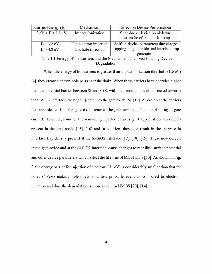
2.2 Carrier Injection and Gate Current
The main cause for hot carrier degradation is due to injection of hot carriers from the
channel into the gate oxide. The injection of carriers at any given location along the channel
is determined by two factors, the concentration of the carriers in the channel and the electric
field at that point of injection [33], [14].
In the subthreshold region, the injection of carriers into gate oxide is negligible
because the concentration of carriers in the channel is very low. As the gate bias increases,
12
the concentration of the carriers in the channel increases and thus the electron and hole
injection current increases.
However, there is always a point of discussion in hot carrier literature whether it is
hot electrons or hot holes responsible for device degradation. It is argued that if holes were
responsible for degradation, then threshold voltage shift in PMOS will be much greater
than in NMOS because PMOS channel is inverted and will be filled with holes; but even
at higher stress voltage, PMOS degradation was less than that of NMOS. Therefore, it was
understood that hot electron injection was more significant than hot hole injection [5].
The relation between injection current, gate current and trapped carriers in a
NMOSFET as a function of gate bias is shown in the figure and is explained below [13].
Figure 2.1 Carrier Injection and Gate Current Vs Gate Bias [14]

13
At low gate voltage, the transverse electric field and the Schottky barrier lowering
favors the hole injection into the oxide more than electron injection and since the oxide
field also favors the transport of injected holes, most of them reach the gate terminal. Thus
at low gate bias, gate current is primarily due injected holes [26], [27].
As the gate bias increases, the Schottky barrier lowering decreases and the electron
injection current increases due to relatively smaller potential barrier for electrons at oxide-
silicon interface. However, the field in the oxide is against the electron transport and thus
most of the injected electrons either scatter back to the interface or gets trapped in the
oxide. Therefore at this bias condition, the gate current is low when compared with electron
injection current.
As gate bias is increased, the opposing oxide field decreases and a larger proportion
of injected electrons contribute to the gate current and thus the gate current peaks when
VGS=VDS.
When VGS > VDS, the lateral electric field decreases causing the electron injection
also to decrease, but the oxide field favors the electron transport to the gate terminal and
thus gate current is almost equal to electron injection current.
Some of the important characteristics of the gate and injection current in NMOS are
[14]:
• Electrons are injected into gate oxide under all gate bias.
• The peak of the hole injection current is smaller than that of the electron injection
current because the oxide-silicon barrier is large for hole injection.

14
• The amount of holes getting trapped in the oxide is negligible when compared with
electrons, since most of the injected holes reach the gate terminal, whereas in the
case of electrons, during the mid-bias region most of the injected electrons gets
trapped in the oxide.
Therefore, it can be concluded that in NMOS, bulk oxide defect generation is due to
hot electrons getting trapped in the gate oxide.
2.3 Interface Trap Generation
Various measurements of the MOSFETs subjected to hot carrier degradation have
showed that besides charges getting trapped in the gate oxide, interface traps are also
generated, and also, under some conditions interface traps are the main cause for device
degradation [34], [35]. Hence an understanding of the interface states and its generation by
hot carrier injected is required and is presented below.
2.3.1 Interface States
Interface states or interface traps are energy levels located at oxide-silicon interface
that can capture or release electrons. They are created due to imperfections like lattice
mismatch, disconnected chemical bonds or impurities [36]. They can be classified into two
types: the interface state which is electrically neutral when occupied by an electron and
positive when the electron is released is called a donor like interface trap, and an acceptor
like interface state is the one which is electrically negative when occupied by electron and
neutral when the electron is released [37]. It is generally assumed that donor like interface
traps are located in the lower half of the bandgap while acceptor like interface traps are
located in the upper half. As the position between energy level and Fermi level varies, the

15
occupation condition of that trap level also varies. Hence the electrical charge of an
interface trap is a function of band bending and gate voltage [5], [37], [38], [39]. Figure
2.2 shows this dependency in a p-substrate MOS capacitor.

16
Figure 2.2 Relationship Between Interface States and Gate Bias at Different conditions
(a) Flatband, (b) Accumulation, (c) Depletion, (d) Mid-gap, (e) Inversion [40]
Vgb is the voltage between the gate and substrate, Vfb is the flat band voltage and Vmid is
the mid-gap voltage at which the intrinsic Fermi level (Ei) reaches the Fermi level (Ef).
Flatband:
When Vgb = Vfb, all the acceptor like interface traps are above Ef and hence they are
electrically neutral. Donor like traps which are present below the Fermi level are neutral
and which are present above the Fermi level are positive. Therefore, in the flatband
condition, only donor like traps above the Fermi level contribute positive charge.
Accumulation:
When Vgb < Vfb, the bands bend up and so the acceptor type traps remain neutral,
on the other hand donor like traps contribute more positive charges.
Depletion:

17
When Vfb <Vgb < Vmid, the band bends down but the acceptor type traps still remain
neutral whereas donor like traps contribute less positive charge.
Mid-gap:
It is a transition point between the depletion and the inversion. As Vgb is increased
and when Vgb = Vmid, Ei touches Ef and during which all interface states are neutral.
Inversion:
When Vgb > Vmid, parts of acceptor like traps below the Fermi level capture electron
and produce negative charge. The other acceptor like traps and donor like traps remain
neutral.
Therefore, based on the voltage applied between the gate and substrate the type and
number of charges present at the oxide-silicon interface varies, contributing to shifts in
threshold voltage, subthreshold slope and transconductance.
2.3.2 Interface Trap Generation Due to Hot Carriers
As seen from the above section, the injected hot carriers sometimes get trapped in
the oxide causing device degradation and in addition to that hot carriers also create interface
traps [13], [5], [41].
Electrons which have lighter effective mass when compared with holes will have
longer mean free path and hence gain more energy and cause high impact ionization rate.
Also, conduction band offset at the oxide-silicon interface is smaller than valence band

18
offset and hence electrons can create interface traps easily by injection over the oxide
barrier [13].
For both PMOS and NMOS, the interface trap (NIT) density peaked at hole
injection regimes and the lack of correlation between substrate current and NIT peak
density was attributed to hot hole induced degradation and also holes were orders of
magnitude more efficient for trap creation [41], [42], [43], [44].
On a related argument, it is still not very clear whether the carriers need to be
injected into the oxide to generate defects. It was claimed that hot electron injection is
necessary to create interface traps, in other words if the electron energy is less than the
conduction band offset then there would be neither electron injection into the oxide nor the
interface traps [13]. Therefore, if the supply voltage is less than 2.5V, hot carrier injection
should be eliminated but the interface traps were created at biases even less than 0.9V [34],
[35], [45]. Also, experiments were conducted by injecting hot electrons from the substrate
into gate oxide and the interface trap density was measured [46]. When a gate bias is
applied, hot electrons produced higher source and drain current but gate current was
reduced drastically. Even in this condition, interface traps were created and hence it can be
concluded that electron injection is not needed for interface trap creation. When the gate
bias was reversed, the gate current and the degradation increased dramatically but the
substrate current did not change [47]. This showed that when carrier injection takes place,
interface trap density increases dramatically.
Therefore, following can be concluded from the above discussion [48]:

19
• Both the hot holes and hot electrons are responsible for interface trap creation.
• Interface trap density is maximum when hot hole injection is maximum and they
are orders of magnitude more efficient than hot electrons.
• Hot carrier injection is not necessary to create interface traps but the density of
interface traps increases dramatically when carrier injection takes place.
2.4 Effects of Hot Carrier Injection on Device Parameters
HCI degrades the device and affects the device parameters, such as threshold voltage,
subthreshold swing, mobility and transconductance by introducing additional trapped
charges and interface states inside the gate oxide [11], [12]. In this section, the relationship
between HCI and these device parameters are discussed.
2.4.1 Hot Carrier Effect on the Threshold Voltage
The effect of additional trapped charges and acceptor like interface traps created
during HCI on the threshold voltage can be given as
V�� = 2ϕ� + 2qN�ϵ��2ϕ� − V���C�� + ϕ�� − Q�C�� − Q��C�� , �2.1�
where, ϕ� is the bulk potential,
NA is the substrate doping concentration,
q is the electron charge,
ϵS is silicon permittivity,
ϕMS is metal semiconductor work function,

20
Q0 is the density of trapped charges in gate oxide,
QIT is the density of interface trap charges,
COX is gate oxide capacitance.
Both the trapped charges (electrons) and interface traps (acceptor like at threshodl)
are electrically negative and hence the threshold voltage of a degraded NMOS increases
which can be seen in the figures below. It is a plot of data obtained from 28nm technology
transistor stressed at 2V [36], [37].
Figure 2.3 Plot Showing Increase in Threshold Voltage Due to Hot Carrier Effect
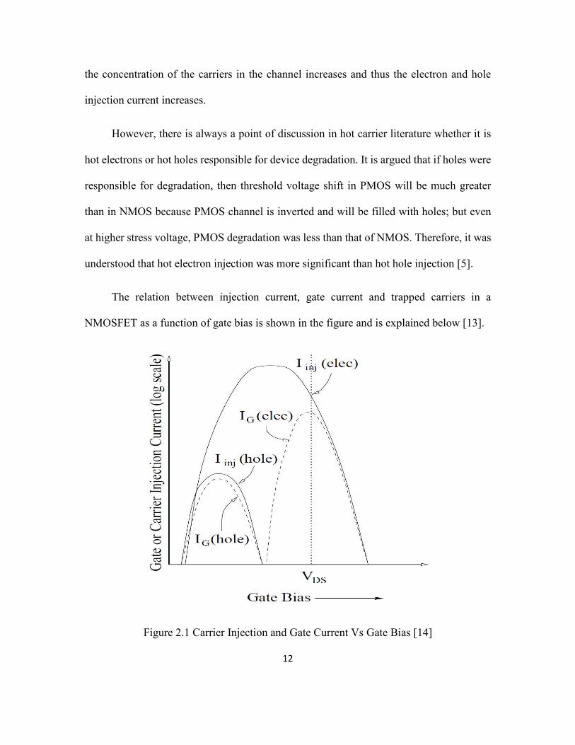
2.4.2 Hot Carrier Effect on the Subthreshold Slope
The subthreshold slope of a degraded device is affected only by the interface traps
and not due to the trapped charges inside the gate oxide [37], [39]. This is because, the total
-5.00E-06
0.00E+00
5.00E-06
1.00E-05
1.50E-05
2.00E-05
2.50E-05
3.00E-05
3.50E-05
-0.4 -0.2 0 0.2 0.4 0.6 0.8 1 1.2 1.4
Dra
in C
urr
ent
Gate Voltage
Drain current vs gate voltage before and after stressing
Pre-stress Post-stress
21
charge contribution by these trapped defects are fixed and independent of the applied bias,
thereby causing only horizontal shift in the log Id versus Vg plot. A capacitance value
proportional to the density of interface traps CIT can be modelled based on the below
equation,
S = �ln10��V!��C�� + C�" + C���C�� , �2.2�
where, S is subthreshold swing (or inverse sub-threshold slope),
Vt is the thermal voltage,
CSC is the semiconductor capacitance,
CIT is the capacitance due to interface states.
Subthreshold swing will increase during HCI since more interface traps are created
which causes larger interface state capacitance. This can be observed in the figure below.
Figure 2.4 Plot Showing Increase in Subthreshold Swing Due to Hot Carrier Effect
1.00E-14
1.00E-10
1.00E-06
1.00E-02
-0.5 0 0.5 1 1.5Log D
rain
Curr
ent
Gate Voltage
Log Drain current vs gate voltage before and
after stressing
Pre-stress Post-stress

22
Figure 2.5 Plot Showing the decrease in Subthreshold Slope Due to Hot Carrier Effect
2.4.3 Hot Carrier Effect on the Mobility
Interface traps created during HCI degrades the mobility of the device by increasing
coulomb scattering. An empirical relation between mobility and interface trap density is
given as follows [49], [50],
μ = μ�1 + αN�� , �2.3�
where, & is the mobility after hot carrier degradation,
μ0 is mobility of the device before degradation,
α is a constant that depends on doping concentration of the substrate and is given as,
α = −0.104 + 0.0193lo g�N�� , �2.4�
where, NA is the doping concentration of the substrate.
1.00E-11
1.00E-09
1.00E-07
1.00E-05
1.00E-03
1.00E-01
0 0.05 0.1 0.15 0.2 0.25 0.3 0.35 0.4 0.45
Log
Su
bth
resh
old
Slo
pe
Gate Voltage
Log Subthreshold slope vs gate voltage before and
after stressing
Pre-stress Post-stress

23
2.4.4 Hot Carrier Effect on the Transconductance
The transconductance of a MOSFET is defined as the derivative of the drain current
versus gate voltage. Therefore, transconductance is given as [39]:
g+ = μ,C��WL �V/� − V��� + 12 C�� 0WL 1 �V/� − V���2 0 δμ,δV/�1 , �2.5�
HCI decreases the mobility and increases the threshold voltage of a degraded devices, both
these parameters lead to decrease in transconductance value as shown in the figure below
[54].
Figure 2.6 Plot Showing Decrease in Transconductance Due to Hot Carrier Effect
2.5 Hot Carrier Degradation in Long Channel MOSFET
The defects caused by HCI are localized in nature and extend for about 50nm -
200nm from the drain. Hence, in a long channel MOSFET conventional uniform defects
-2.00E-05
0.00E+00
2.00E-05
4.00E-05
6.00E-05
8.00E-05
1.00E-04
1.20E-04
-0.4 -0.2 0 0.2 0.4 0.6 0.8 1 1.2 1.4
Tra
nsc
ond
uct
ance
Gate Voltage
Transconductance vs gate voltage before and after
stressing
Pre-stress Post-stress

24
characterization techniques such as mid-gap techniques cannot be used [37], [51].
Whereas, in MOSFETs with channel length less than 50nm the defects are distributed all
along the channel. Therefore in long channel MOSFET, because of non-uniform defect
nature, the concept of single threshold voltage loses its meaning and two-piece transistor
model is used to overcome this problem [51]. In this section, a detailed review of this defect
localization, problems in characterizing because of it and a technique to overcome it is
presented.
2.5.1 Location of Defects
When MOSFETs are biased in the saturation region of operation, the pinch off
region appears near the drain terminal. Due to the existence of high field in the pinch off
region, the carriers gain enough energy and undergo impact ionization generating electron-
hole pairs which undergoes carrier injection. The carrier injection and defect generation
are non-uniform along the channel because they depend on the local values of the carrier
energy and vertical component of electric field [51].
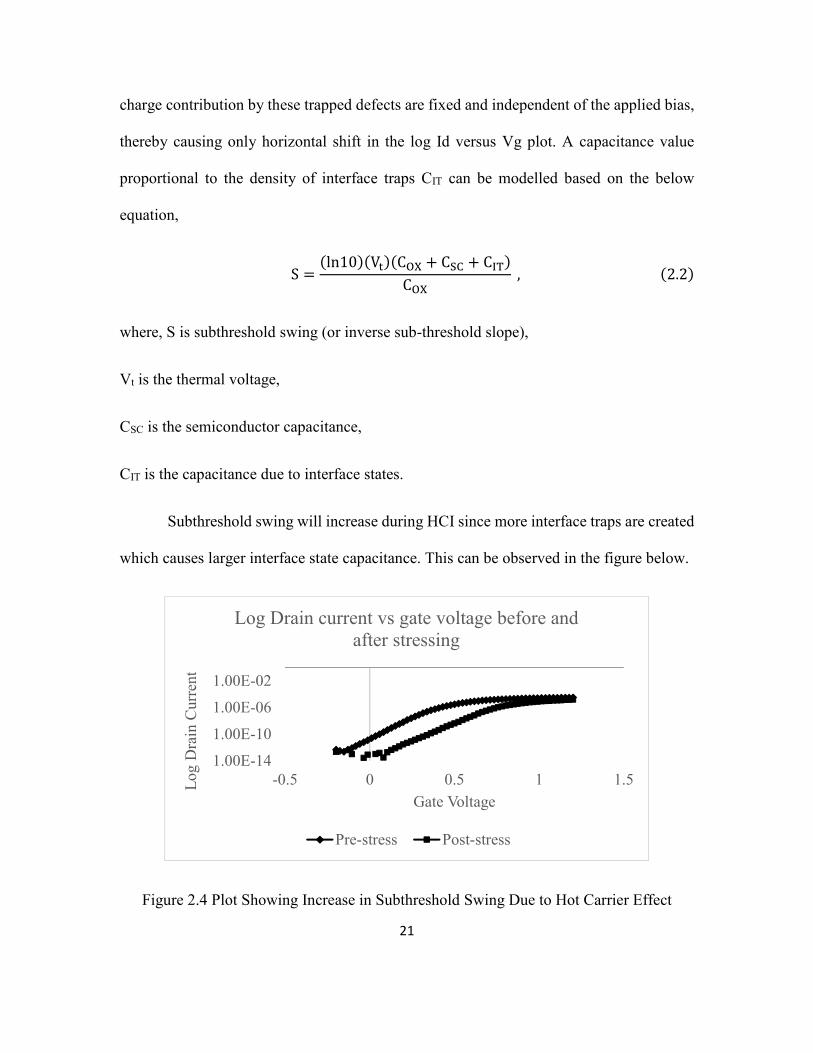
Evidence for the localized nature of the defects is found in the asymmetrical
behavior of the drain current characteristics, measured in the normal and reverse (source
and drain interchanged) modes of operation. In the normal mode, as the drain bias increases
the pinch off region expands towards the source and covers a larger portion of the defect
region. As a result, the minority carriers flow far from the interface and are less affected
due to the defects created. Therefore, the larger the drain bias the contribution due to
damaged region is less and the drain current characteristics approaches that of non-
degraded device. On the contrary, when the drain and source terminal are interchanged, the
25
reverse mode drain current is always less than that of non-degraded device because the
damaged region of the channel falls inside the inversion region for all values of drain bias
and so the defects are always active causing maximum degradation to drain current
characteristics [14], [52]. This can be clearly seen in drain current versus drain bias plot
shown in the figure below.
Figure 2.7 Normal and Reverse Mode Drain Current Vs Drain Bias Measured Before and
After Hot Carrier Stress in NMOSFET [14]
The data above suggests that the defects generated due to HCI are localized near
the pinch off region and it has been shown that the spreading of the defective region varies
from 50nm to 200nm depending on the bias applied.

26
2.5.2 Problems Caused Due to Defect Localization in Measuring Degradation Parameters
During substrate hot carrier injection experiments, the carrier injection is uniform
along the channel and the drain current characteristics can be used to provide details about
the degradation processes [53], [54]. However, during drain avalanche hot carrier injection
the carriers are injected into the gate-oxide in a localized region close to the drain and
therefore, the interpretation of the parameter variations during non-uniform channel hot
carrier injection based on the results obtained from uniform injection experiments can be
highly inaccurate [51]. For example,
The change in drain current versus gate bias characteristics can be used to measure
the density of interface traps and trapped charges in the gate oxide using the mid-gap
voltage technique. This technique assumes that the change in subthreshold slope is entirely
due to interface traps and the trapped charges cause only a parallel shift in the subthreshold
characteristics of the drain current [37]. However, studies have shown that a localized oxide
charge can also cause a change in subthreshold slope making the mid-gap technique
useless.
When there is uniform injection of carriers, the threshold voltage at each point
along the channel shifts by the same amount and therefore the threshold voltage of the
complete device is equivalent to that of any point along the channel. However, during non-
uniform injection of carriers, the threshold voltage at each point can be different due to
localization of the defects. Hence, the definition of a single threshold voltage for an entire
device loses it physical meaning [51].

27
2.5.3 Two-Piece Model
Most of the models which describe the hot carrier induced degradation do not
account for defect localization and the defects are averaged over the entire channel length
as if they were uniformly distributed [51].
Therefore, in order to have better understanding about the degraded parameter
variation, the damaged transistor is considered as two transistors connected in series. One
transistor with channel length equal to length of defective region with defects uniformly
spread across the entire channel and the other transistor with no defects and channel length
equal to length of non-defective region [55]. They are connected in series as shown in the
figure.
Figure 2.8 Schematic of Two Transistor Model
Let G1 and G2 be the conductance of the defect free and defective channel transistor and
Ga and Gb are the conductance after and before HCI.
G6 = G7G2G7 + G2 , �2.6�

28
From the figure, it can be found that at the onset of strong inversion, the
conductance G2 is very much lower than Gl and it is the defective region which dominates
the current conduction through the channel. Whereas in the strong inversion, the defect free
region regains the full control of the current conduction in the device.
Figure 2.9 Channel Conductance Vs Gate Voltage [51]
Therefore, according to the two-piece model, the threshold voltage of a degraded device
is the local threshold voltage value of the defective region. The damaged region exhibits a
very low conductance when compared to the rest of the channel and no appreciable
conduction takes place unless the gate bias exceeds the local threshold voltage of the
defective region. On the other hand, one-piece model considers only one threshold value
and it includes the average value of localized defects along the entire channel [51], [55].

29
3 HOT CARRIER INJECTION MODELS
3.1 Introduction
Theoretical work on hot carrier injection and its effects on the devices was started in
early 1950s but the modelling was not started until 1980 [56]. This is mainly because, there
is still debate going on about the different mechanisms involved in hot carrier injection
such as, what charges get injected and whether charge injection is required to cause device
degradation [11], [43].
However, experimental techniques have showed that hot carrier degradation is due
to charge trapping and generation of interface traps and thus by measuring the device
degradation parameters some models have been formulated [43], [57]. The lucky hot
electron model proposed by Shockley is the widely-used model in studying the hot electron
injection and using this, the gate current of the transistors was calculated theoretically [27],
[13], [58]. Initially, the gate current was used to model the hot carrier effects but
experiments have failed to show a good correlation between the gate current and defects
created [11], [59], [60].
However, substrate current of MOSFETs have shown higher correlation to device
degradation and by incorporating lucky electron model in substrate current calculation,
relation between interface traps generated and substrate current was formulated [11], [60].
The problem with the above technique is that it considers only interface trap generation
and not trapped charges in device degradation [11]. In this chapter, the concept of lucky

30
electron model is initially described and then the substrate current calculation based lucky
electron model is presented.
3.2 Lucky Electron Model
The lucky electron model formulated by Shockley is one of the successful gate
current models used in MOSFETs [61]. In this model, four statistically independent
probabilities are calculated and the total probability corresponds to that of an electron
travelling from the source to drain along the channel, being successfully able to overcome
the potential barriers and get injected into the gate oxide and thus contributing to the gate
current [27], [58], [61], [30], [62].
In order to quantify the probability that these electrons could be injected into the gate
oxide, several types of scattering events have to be considered. Figure 3.1 shows an energy
band diagram drawn normal to the Si-oxide interface along a cross section of the MOSFET
in Figure 3.3.
31
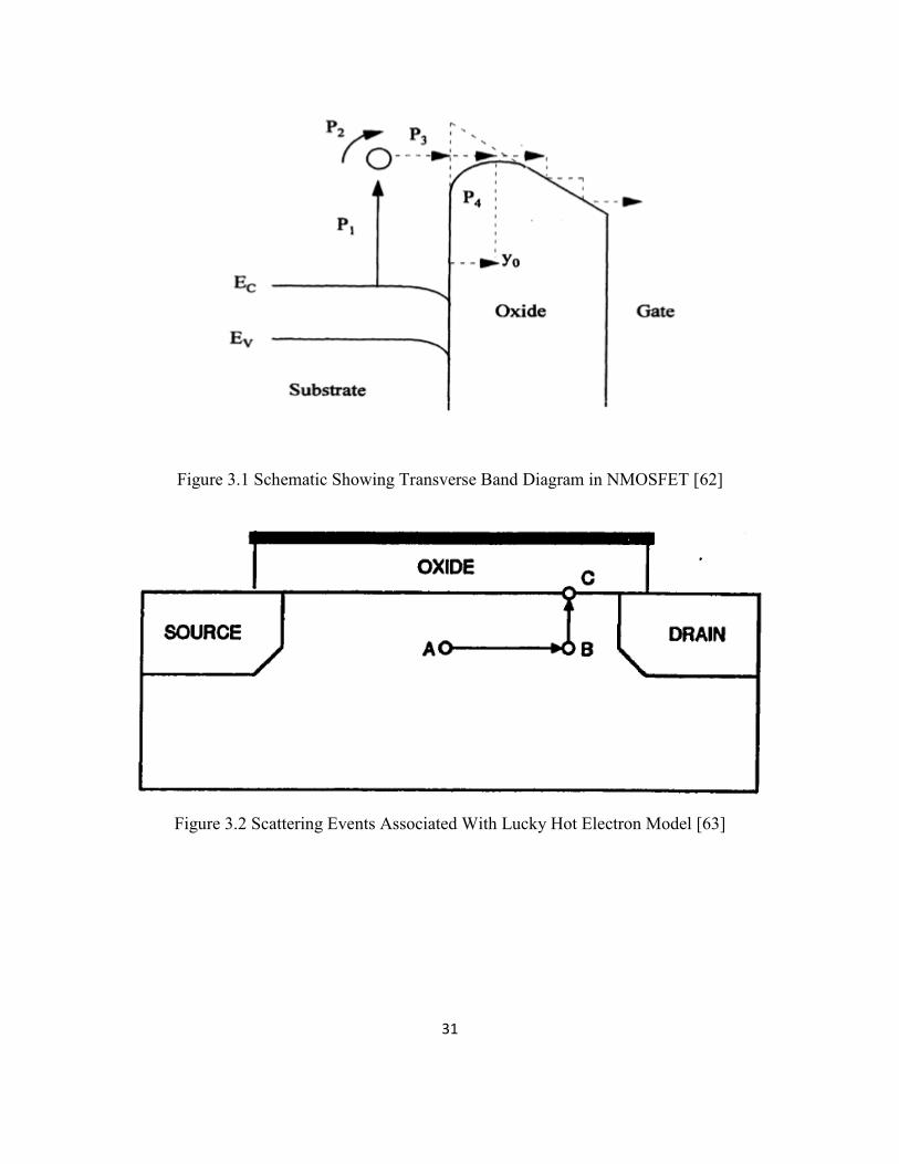
Figure 3.1 Schematic Showing Transverse Band Diagram in NMOSFET [62]
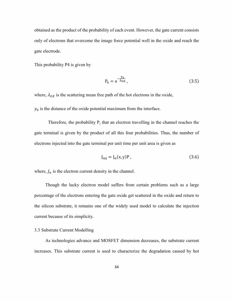
Figure 3.2 Scattering Events Associated With Lucky Hot Electron Model [63]

32
Figure 3.3 The Probabilities Associated With Lucky Hot Electron Model [62]
In Figure 3.2, an electron moving along the channel from point A to B, gains enough
kinetic energy from the lateral electric field to cross the oxide-silicon interface potential
barrier and this probability P1 is given by
P7 = e;<= = e; >?@A= , �3.1�
where, BC is the Schottky lowered barrier between silicon and gate oxide,
D is the distance an electron need to travel to acquire energy greater than BC,
Ex is the constant accelerating electric field between point A and B,
λ is the scattering mean free path of the hot electron in the silicon.
At point B, since the electron is travelling parallel to the interface, its momentum
has to be redirected normal to the interface by an elastic collision. It should be noted that

33
this collision should not be an energy robbing collision, so that the electron will retain the
kinetic energy required to surmount the oxide-silicon potential barrier and hence it is called
quasi-elastic collision. Therefore, P2 gives the probability of this collision to take place
and it is given by:
P2 = 12 D1 − EϕFϕ G , �3.2�
Thus, by integrating the product of P1 and P2 over all energies phi, the probability
of an electron having enough normal momentum to surmount the oxide-silicon potential
barrier can be calculated as,
P7P2 = 14 0EIλϕF 1 e; >?@K= , �3.3�
After the quasi-elastic collision, the electron must travel from point B to C at the
interface without undergoing any further collisions so that its momentum does not get
redirected or its kinetic energy does not get diminished. The probability P3 of this
happening is given by,
PL = e;M= , �3.4�
where, y is the distance between point B and C.
Therefore, if the electron reaching the oxide interface has sufficient kinetic energy
to overcome the oxide potential barrier, then it gets injected into the gate oxide. Since all
the above three events are statistically independent, the carrier injection probability can be
34
obtained as the product of the probability of each event. However, the gate current consists
only of electrons that overcome the image force potential well in the oxide and reach the
gate electrode.
This probability P4 is given by
PN = e; MO=PQ , �3.5�
where, RST is the scattering mean free path of the hot electrons in the oxide,
U� is the distance of the oxide potential maximum from the interface.
Therefore, the probability P, that an electron travelling in the channel reaches the
gate terminal is given by the product of all this four probabilities. Thus, the number of
electrons injected into the gate terminal per unit time per unit area is given as
JW,X = J,�x, y�P , �3.6�
where, [\ is the electron current density in the channel.
Though the lucky electron model suffers from certain problems such as a large
percentage of the electrons entering the gate oxide get scattered in the oxide and return to
the silicon substrate, it remains one of the widely used model to calculate the injection
current because of its simplicity.
3.3 Substrate Current Modelling
As technologies advance and MOSFET dimension decreases, the substrate current
increases. This substrate current is used to characterize the degradation caused by hot

35
carrier injection because in both the device degradation and the substrate current the lateral
electric field in the channel is the driving force [11], [60].
3.3.1 Origin of Substrate Current
When the MOSFET operates in the linear regime, the drain current increases
linearly as the drain voltage increases. However, as the drain voltage is further increased,
the channel thickness at the drain end gets reduced and at the voltage VD = VDSAT, the
inversion layer gets pinched off. This corresponding voltage is called saturation drain
voltage and if the drain voltage is increased beyond this point several important events
occur: the length of the pinched off region increases and the voltage at the end of pinched
off region remains sat Vdsat even if Vd increases. Therefore, the drain current remains
almost constant but the electric field in the pinch off region increases rapidly. Due to this
high electric field, electrons get accelerated and undergo several kinds of scattering events
[62]. One such event is called impact ionization, where the electrons undergo collisions
with the lattice and generates electron hole pairs. The holes created by this process are
collected by the substrate and constitute the substrate current [11], [60]. Therefore, the
substrate current can be given as
I^_F = I<rWW , �3.7�
where, bcc is the impact ionization rate which is dependent on the concentration of electrons
in the channel and the lateral electric field.
Figure 3.4, is the plot of substrate current as a function of gate voltage for different
drain voltages. Initially, when the gate voltage increases, the concentration of the electron

36
in the channel increases due to attraction by the gate voltage and hence substrate current
increases. However, after a certain gate voltage, the lateral field in the channel decreases
as shown in the Figure 3.5. This decrease in lateral electric field causes a decrease in
substrate current. Thus, the change in equilibrium between the electron concentration and
lateral electric field yields the bell shaped substrate current characteristics. The peak of the
substrate current occurs at VG = VD/2 for older technology MOSFETs and at VG = VD for
latest technologies [11], [62].
Figure 3.4 Plot Showing Substrate Current Vs Gate Bias for Different Drain Bias
0
0.2
0.4
0.6
0.8
0 2 4 6 8
I su
b (
mA
)
VG (V)
VD=7 V6.8 V
6.6 V6.4 V
6.2 V6.0 V

37
Figure 3.5 Plot Showing Decrease in Lateral Electric Field as Gate Bias Increased
3.3.2 Substrate Current Model Based on Lucky Electron Model
Using the lucky electron model approach, the impact ionization rate due to channel
carriers can be calculated [64]. The electrons travelling along the channel must gain enough
kinetic energy for generating electron-hole pairs through impact ionization process. The
distance an electron needs to travel under the influence of the electric field in order to gain
energy Bc is given by
d = ϕWqE+ , �3.8�
where, Bc is the minimum energy required for by an electron to create impact ionization
process.
Em is the maximum electric field in the channel.
-1.20E+06
-7.00E+05
-2.00E+05
3.00E+05
0.00E+00 1.00E-02 2.00E-02 3.00E-02 4.00E-02 5.00E-02
Lat
eral
E-f
ield
Distance from source towards drain
Distance from source towards drain vs Lateral E-field for
different gate bias and fixed drain bais (0.5V)
E-Field (Lateral) - 0.4V E-Field (Lateral) - 0.8V
E-Field (Lateral) - 1.2V

38
Thus the probability of an electron traveling a particular distance to be able to gain
sufficient energy without undergoing a collision is given by
PW = e; >fg=@h , �3.9�
where, λ is the electron mean free path in the channel.
The drain current gives a measure of electron flow in the channel and the product
of Pi*Ids will give the rate at which electrons having energies greater than ϕi are supplied
by the drain current. Therefore,
I^_F = CI<^e; >fg=@h , �3.10�
where, C is a function of Em.
The interface traps created due to impact ionization can be calculated similarly. If
the electron or hole have kinetic energy greater than what is required to break an oxide
bond, then an interface trap will be created by them [64]. Let Bij,k and Bij,l be the energies
required by the electrons and holes to create an interface trap and these values are found to
be Bij,k=3.7eV and Bij,l=4.2eV which are determined experimentally.
Therefore, the portion of the drain current with electrons having kinetic energy greater than
Bij,k can be given as
I��,@ = C1W I<^e; >mn,og=p@h , �3.10�
where, qrr,k is the bond breaking electron current.

39
Rs is the mean free path of electrons in the channel.
Similarly, the portion of the substrate current with holes having kinetic energy greater than
Bij,l can be given as
I��,t = C2W I<^e; >mn,ug=v@h , �3.11�
where, qrr,l is the bond breaking hole current.
λh is the mean free path of holes.
The values of Rs and λh are 6.7nm and 4.9nm respectively.

40
4 ANALYTICAL MODEL FOR HOT CARRIER DEGRADATION
4.1 Introduction
Most of the existing hot carrier degradation models do not consider the physics
involved in the degradation process and they just calculate the change in threshold voltage
for different stress voltages and time. Based on this threshold voltage shift, the lifetime of
the device is predicted [65], [32], [11]. However, as seen from the previous chapters, hot
carrier injection causes two types of traps namely, gate oxide trapped charges and interface
traps and the effect of these traps on device parameters are different. Hence, the density of
each type of traps created must be calculated individually.
In this chapter, a simple analytical model which calculates the density of trapped
charges and interface traps is derived. In order to find out the parameters present in the
analytical model, devices are stressed at different voltages and using the charge separation
technique the density of trapped charges and interface traps are calculated. Once the
parameters are determined, the validation of the analytical model is perform using TCAD
simulations. Finally, the surface potential method is used to calculate the threshold voltage
shift due to each type of traps and is incorporated in Verilog-A.
4.2 Derivation of Analytical Model
When an electron in the conduction band gain enough kinetic energy, then it might
collide with the lattice and transfer its energy to the lattice causing it to break a bond and
generate electron hole pairs. This process is called impact ionization as discussed in the
previous section. These electron hole pairs generated by impact ionization can in turn gain

41
energy from the high electric field exiting in the pinch off region and further produce more
electron hole pairs making it as a chain reaction. Such a chain reaction is called as
avalanche impact ionization or avalanche multiplication and the electrons or holes
generated by this method are called avalanche hot electrons or avalanche hot holes
respectively [11], [62].
Figure 4.1 Carrier Multiplication Due to Impact Ionization [62]
At this point, when the drain voltage is increased, a sharp increase in the drain
current is observed and this is called breakdown phenomenon and the drain voltage at
which it occurs is called drain to source breakdown voltage. While the electrons generated
reach either the drain electrode or the gate terminal, the holes move towards the substrate
contributing to substrate current. This causes the potential of the substrate to increase above
the source terminal and hence the potential barrier between the source and substrate gets
lowered, which in turn further enhances electron injection and the drain current like a
positive feedback loop [66].

42
Avalanche multiplication induced current can be given as
I< = MI^ , �4.1�
where, Id and Is are the drain and source currents.
M is the multiplication factor and it can be given as
M = 11 − IWx, , �4.2�
where, Iion is the ionization integral which can be defined as
IWx, = y α,e; z �{|; {}�<IA dx~, �4.3�
where, �\ and �� are the ionization rates of electrons and holes respectively. In order to
understand hot carrier degradation, it was realized that an accurate model calculating the
electric field is required [67], [68]. By using the pseudo two dimensional approximation
and Poisson's equation, an expression for electric field in the channel is derived as
���� = ����cos h �� − ����� � , �4.4�
where, Esat is the critical electric field needed for velocity saturation,
x is the distance from the source in the channel towards drain,
l is the effective length of the velocity saturation region,
xsat is the point at which E equals Esat.
Using the above expression the maximum electric field in the channel is given as

43
E+ = �A2�V<^ − V<^6!�2 + E^6!2 , �4.5�
Thus the substrate current can be expressed as,
I^_F = αWβW I<^�V<^ − V<^6!�e; ���;����� , �4.6�
where, �c and �c are impact ionization coefficients and A is a fitting parameter [62], [69],
[70]. Substrate current gives a quantitative measurement of the number of holes, and
therefore electrons, generated through impact ionization.
A simple model to estimate the density of trapped charges and interface traps
generated is formulated using the above model. If the device is stressed for t seconds and
Isub is the substrate current, then the total amount of charges generated can be given as,
Q = I^_Ft , �4.7�
Some percentage of these charges will contribute to generation of interface traps
and some will get trapped in the gate oxide. Therefore, the density of trapped charges and
interface traps generated can be given as,
Nx! = k,x!Q , �4.8�
NW! = k,W!Q , �4.9�
where, Knot and knit are the fitting parameters which are determined using the experimental
data.

44
Since the substrate current depends on gate and drain voltages, the analytical formula
used here to calculate the device degradation is a function of these stress voltages and stress
time.
4.3 Model Parameterization and Validation
As presented above, the analytical model used in this thesis is based on the substrate
current and the amount of charges created by them.
I^_F = αWβW I<^�V<^ − V<^6!�e; ���;����� , �4.10�
where, �c and �c are impact ionization coefficients and A is the parameter which is
dependent on the applied stress voltage.
From the substrate current, the density of trapped charges and interface traps
generated can be given as,
Nx! = k,x!I^_Ft , �4.11�
NW! = k,W!I^_Ft , �4.12�
where, t is the amount of time the device is stressed for a given stress voltage and knot and
knit are the fitting parameters. Therefore, the parameters which need to be calculated using
the experimental data are knot, knit and A, in which knot and knit are constant for all stress
voltages and A depends on the applied stress voltage.
Following the model parametrization, using the analytical model, the density of
trapped charges and interface traps generated are calculated for different stress voltages

45
and compared against the results of TCAD simulations to verify the accuracy of the model
and the parameters obtained.
In the next section, a method used to separate the density of oxide trapped charges
and interface traps generated from the drain current characteristics is presented and the
traps generated are calculated from the data for different stress voltage. Finally, the various
parameters are calculated and is validated against TCAD simulations.
4.3.1 Charge Separation Technique
As seen from previous chapters, hot carrier injection in MOSFET causes interface
trap generation and charge trapping in gate oxide, thereby causing change in sub-threshold
slope and threshold voltage of the device. The total threshold shift due to these two defects
can be given as [37], [71],
δV�� = δV,x! + δV,W! , �4.13�
where ��\�� is threshold shift due to oxide trapped charges and
���c� is the threshold shift due to interface traps.
Two techniques are available to calculate the trapped charge density and interface
trap density from the device characteristics [71], [72]. The inversion characteristics
technique uses Brews charge sheet model to fit the experimental data and it requires an
empirical coefficient, actual physical dimensions of the transistors and other process
parameters which are not easily available [72], [73]. The other technique namely, mid-gap
voltage method requires only the gate oxide thickness and the substrate doping which are
easier to extract using the data and TCAD simulations and also in the case of short channel

46
MOSFETs, the defects are spread across the entire channel length. Hence the mid-gap
voltage method can be employed.
The assumptions made in this method are [37]:
1. The negative fixed trapped charge (electron) density is a sheet of charge at the interface
which is spread across the entire channel length and
2. Acceptor like interface traps are present only in the upper half of the bandgap and donor
like interface traps are present only in the lower half of the bandgap. Therefore, when the
surface potential is equal to the bulk potential that is when the Fermi level touches the
intrinsic level at the interface, the net charge contribution by the interface states are zero
and this corresponding voltage is called mid-gap voltage.
In NMOS, the interface traps generated decrease the subthreshold slope and
increase the threshold voltage whereas, the trapped electrons cause only increase in
threshold voltage. Since at the mid-gap voltage the interface traps are neutral, the change
in drain current characteristics in the Id-Vgs plot is only due to charges trapped in the oxide
[37], [71]. Thus the shift in the mid-gap voltage level (����) is equal to voltage shift due
to trapped electrons (��\��), that is,
δV+� = δV,x! , �4.14�
and the threshold shift due to interface states can be calculated from the total threshold
voltage shift by,
δV,W! = δV�� − δV,x! , �4.15�

47
The drain current in the subthreshold region is given by [5]:
I< = μ 0WL 1 0aC��2β2 1 0 nWN�12 �1 − e; ��¡ ¢ e >�βϕ^£ , �4.16�
where
a = √2ϵ^C��L¥ , �4.17�
L¥ = E ϵ^βqN� , �4.18�
And where & is the mobility of the electron in the channel,
¦§ is the Debye length,
W is the width of the transistor,
L is the channel length,
Cox is the gate oxide capacitance,
NA is the doping concertation of the substrate,
ni is intrinsic,
B� is the surface potential;
The mid-gap current can be calculated from the above equation by using,
B� = BC = ¨©ª l n 0«¬c 1 , �4.19�

48
where, BCis the bulk potential.
Therefore,
I+� = μ 0WL 1 0aC��2β2 1 0 nWN�12 �1 − e; ��¡ ¢ e >?βϕF£ , �4.20�
The mid-gap voltage is the gate voltage at which drain current equals Img and since
this current is less than that of leakage current, the drain current must be extrapolated to
determine the mid-gap voltage [71].
Threshold voltage is the voltage at which surface potential is twice that of the bulk
potential. So the drain current at the threshold voltage can be found by using,
ϕ^ = 2ϕF = 2 kTq ln 0N�nW 1 , �4.21�
Therefore,
I�! = μ 0WL 1 0aC��2β2 1 0 nWN�12 �1 − e; ��¡ ¢ e2 >?2βϕF£ , �4.22�
The voltage that corresponds to this current in the drain current vs gate voltage
characteristics gives us the threshold voltage.

49
Figure 4.2 Plot Showing Log Drain Current Vs Gate Voltage and Mid-gap Current and
Threshold Voltage Current
4.3.2 Extraction of Fixed Charge and Interface Trap Density from the Data
In order to find out the values of different parameters, five different devices are
stressed at different voltages. The value of gate oxide thickness and substrate doping is
calculated by matching the pre-stressed data of each device with TCAD simulations. Plots
showing the pre-stress data and TCAD simulations are shown below. The difference in
drain current characteristics at higher gate voltage is because of the different mobility
models available in TCAD.
A small difference between each device's oxide thickness and doping concentration
was observed which is due to process variability. The table attached below shows each
device gate oxide thickness, their doping concentration and the applied stress voltage.

50
Stress Voltage (V)
Gate Voltage = Drain
Voltage
Doping
Concentration
(cm-3)
Gate Oxide
Thickness (cm)
Device 1 1.2 6.8E18 1.1E-7
Device 2 1.4 5.3E18 1.3E-7
Device 3 1.6 5.9E18 1.3E-7
Device 4 1.8 5.9E18 1.2E-7
Device 5 2 6.1E18 1.1E-7
Table 4.1 Each Device’s Doping Concentration, Oxide Thickness and the Voltage at
Which They Are Stressed
Since the oxide thickness and substrate doping are known, the mid-gap current and
the threshold current for each device can be calculated using the subthreshold drain current
equation which is given by [89],
I< = μ 0WL 1 0aC��2β2 1 0 nWN�12 �1 − e; ��¡ ¢ e >�βϕ^£ , �4.23�
From the above equation, the mid-gap current can be calculated by substituting,
ϕ^ = ϕF = kTq ln 0N�nW 1 , �4.24�
Similarly, the threshold current can be found by substituting,
ϕ^ = 2ϕF = 2 kTq ln 0N�nW 1 , �4.25�
The Img and Ivth for each device is listed in the below table. The mid-gap voltage method is
used to extract the oxide trapped charge density and interface trap density as seen from the
above section [37], [71].

51
Both the pre-stressed and post-stressed drain currents are extrapolated in the log Id
vs gate voltage plot as shown in the Figure 4.2. The voltage corresponding to mid-gap
current and threshold current is found for both the pre-stressed and post-stressed condition
in all the five devices.
Mid-gap
Current
(A)
IMg
Threshold
Current (A)
ITh
Mid-gap Voltage (V)
VMg
Threshold Voltage (V)
VTh
Pre-stress Post-stress Pre-stress Post-stress
Device 1 6.68E-16 3.21E-7 -0.30472 -0.30278 0.367682 0.369993
Device 2 7.61E-16 2.85E-7 -0.37705 -0.37375 0.313298 0.319828
Device 3 7.19E-16 3.01E-7 -0.32832 -0.27975 0.349384 0.413454
Device 4 7.19E-16 3.01E-7 -0.34368 -0.24123 0.330669 0.475805
Device 5 7.07E-16 3.05E-7 -0.33847 -0.12845 0.320869 0.667041
Table 4.2 Mid-gap Current and Threshold Voltage Current for Different Device and the
Corresponding Mid-gap Voltage and Threshold Voltage for Pre-stress and Post-stress
Condition
The change in mid-gap voltage between pre-stressed and post-stressed condition
gives the change in voltage due to trapped charges since interface traps are neutral at this
condition.
Therefore,
δV+� = δV,x! , �4.26�
The threshold shift due to interface traps alone can be given by;
δV,W! = δV�� − δV,x! , �4.27�
The table attached gives ��j¯, ��\�� and ��\c� for each of device. From ��\�� and ��\c�,
the density of trapped charges and interface traps can be calculated by;
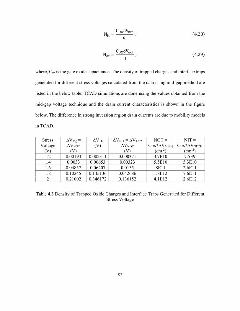
52
NW! = C��δV,W!q , �4.28�
Nx! = C��δV,x!q , �4.29�
where, Cox is the gate oxide capacitance. The density of trapped charges and interface traps
generated for different stress voltages calculated from the data using mid-gap method are
listed in the below table. TCAD simulations are done using the values obtained from the
mid-gap voltage technique and the drain current characteristics is shown in the figure
below. The difference in strong inversion region drain currents are due to mobility models
in TCAD.
Stress
Voltage
(V)
∆VMg =
∆VNOT
(V)
∆VTh
(V)
∆VNIT = ∆VTh -
∆VNOT
(V)
NOT =
Cox*∆VMg/q
(cm-2)
NIT =
Cox*∆VNIT/q
(cm-2)
1.2 0.00194 0.002311 0.000371 3.7E10 7.5E9
1.4 0.0033 0.00653 0.00323 5.5E10 5.3E10
1.6 0.04857 0.06407 0.0155 8E11 2.6E11
1.8 0.10245 0.145136 0.042686 1.8E12 7.6E11
2 0.21002 0.346172 0.136152 4.1E12 2.6E12
Table 4.3 Density of Trapped Oxide Charges and Interface Traps Generated for Different
Stress Voltage

53
Figure 4.3 Plot Showing Pre-stress and Post-stress of Both Data and TCAD Simulation
With Density of Traps Value Obtained Using Mid-gap Voltage Method
4.3.3 TCAD Validation
From the substrate current equation, the parameter A can be expressed as,
A = xln�cx� �4.30�
where, c is a constant and
x is a function of applied stress voltage and drain current.
The above expression can be expanded using the Taylor series and thus and thus
the parameter A can be written as a function of stress voltage in the quadratic form.
In order to get an approximate value of the parameter A, the substrate current and
the drain current are measured for different stress voltages. Having known the substrate
1.00E-16
1.00E-14
1.00E-12
1.00E-10
1.00E-08
1.00E-06
1.00E-04
1.00E-02
1.00E+00
-0.5 0 0.5 1 1.5
Log D
rain
curr
ent
Gate bias
Log drain current vs gate voltage
Pre-stress (Data) Pre-stress (TCAD)
Post-stress (Data) - 2V Post-stress (TCAD) - 2V

54
current, the density of oxide trapped charges and interface traps, the parameters knot and
knit can be calculated as follows,
k,x! = Nx!qI^_F , �4.31�
k,W! = NW!qI^_F , �4.32�
The validation of the analytical model is done using TCAD simulations and the
data. From the analytical model, the density of trapped charges and interface traps
generated are calculated for different stress voltages and the table below shows these
values. Using these trap values in TCAD, the drain current characteristics are calculated
for different stress voltages and is compared against the data. The plots are shown below.
Stress
Voltage
(V)
NOT (cm-2)
NIT (cm-2)
Analytical
model
From Data Analytical model From Data
1.2 3E10 3.7E10 1.6E10 7.5E9
1.4 6.6E10 5.5E10 3.7E10 5.3E10
1.6 5.1E11 8E11 2.8E11 2.6E11
1.8 1.5E12 1.8E12 8.2E11 7.7E11
2 4.2E12 4.1E12 2.3E12 2.6E12
Table 4.4 Density of Traps Calculated Using Analytical Model and from the Data

55
Figure 4.4 Plots Comparing Post-stress Condition Between Analytical Method and Data
Figure 4.5 Plot Comparing Not Calculated Using Analytical Model and Using Data
1.00E-16
1.00E-13
1.00E-10
1.00E-07
1.00E-04
1.00E-01
-0.4 -0.2 0 0.2 0.4 0.6 0.8 1 1.2 1.4
Log D
rain
Curr
ent
Gate Voltage
Log drain current vs gate voltage
Post-stress (Data) - 1.8V Post-stress (Analytical) - 1.8V
Post-stress (Data) - 2V Post-stress (Analytical) - 2V
0.00E+00
5.00E+11
1.00E+12
1.50E+12
2.00E+12
2.50E+12
3.00E+12
3.50E+12
4.00E+12
4.50E+12
1.2 1.3 1.4 1.5 1.6 1.7 1.8 1.9 2
Den
sity
of
trap
ped
ch
arge
Stress Voltage
Density of oxide trapped charges vs stress voltage
Data Analytical

56
Figure 4.6 Plot Comparing Nit Calculated Using Analytical Model and Using Data
4.4 Incorporating the Analytical Model Using Surface Potential Method
Using the analytical expression, the density of oxide trapped charges and interface
traps generated are calculated. However, in order to use them in circuits, the effect of these
traps on device parameters have to be calculated using a surface potential method and must
be incorporated using Verilog-A [74], [75]. In this method, the effect of oxide trapped
charges and interface traps on surface potential are modelled and using the surface potential
– gate voltage relationship, the total impact on the device is calculated.
According to Gauss theorem, the amount of charge per unit area is given as,
Q^ = −ϵ^E^ = −sgn�ϕ^�Q�H�βϕ^� , �4.33�
Q� = 2qϵ^ϕ!N� , �4.34�
0.00E+00
5.00E+11
1.00E+12
1.50E+12
2.00E+12
2.50E+12
3.00E+12
1.2 1.3 1.4 1.5 1.6 1.7 1.8 1.9 2
Den
sity
of
inte
rfac
e tr
aps
Stress Voltage
Density of interface traps generated vs stress voltage
Data Analytical
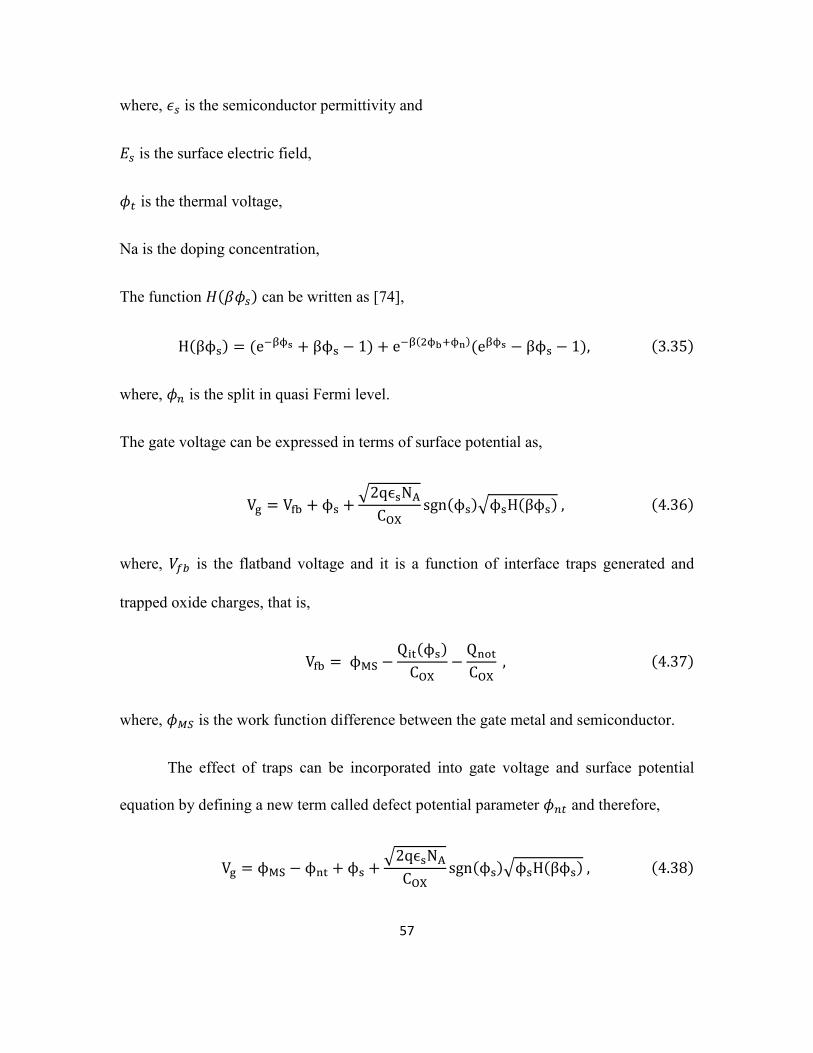
57
where, ±� is the semiconductor permittivity and
�� is the surface electric field,
B� is the thermal voltage,
Na is the doping concentration,
The function ²��B�� can be written as [74],
H�βϕ^� = �e; >� + βϕ^ − 1� + e; �2>?³>|��e >� − βϕ^ − 1�, �3.35�
where, B\ is the split in quasi Fermi level.
The gate voltage can be expressed in terms of surface potential as,
V� = V́ F + ϕ^ + 2qϵ^N�C�� sgn�ϕ^�ϕ^H�βϕ^� , �4.36�
where, �µC is the flatband voltage and it is a function of interface traps generated and
trapped oxide charges, that is,
V́ F = ϕ�� − QW!�ϕ^�C�� − Q,x!C�� , �4.37�
where, B¶· is the work function difference between the gate metal and semiconductor.
The effect of traps can be incorporated into gate voltage and surface potential
equation by defining a new term called defect potential parameter B\� and therefore,
V� = ϕ�� − ϕ,! + ϕ^ + 2qϵ^N�C�� sgn�ϕ^�ϕ^H�βϕ^� , �4.38�

58
where,
ϕ,! = qC�� �Nx! − DW!�ϕ^ − ϕF�¡ , �4.39�
Using the analytical model, the density of traps created are calculated and based on
which the defect potential is found out and correspondingly the effective gate voltage.
Finally, this is incorporated in circuits using Verilog-A.

59
5 CONCLUSION
In this thesis, various hot carrier injection mechanisms and the reason for more
degradation in NMOSFET was discussed. Hot carrier injection causes degradation in
devices due to carrier injection in gate oxide and due to generation of interface traps. The
effect of these traps are different, while trapped charges contribution to device parameters
are independent of applied gate bias, the effect of interface traps depend on gate bias. For
instance, only interface traps cause change in the subthreshold slope of drain current
characteristics whereas, trapped charges do not cause any change to subthreshold slope if
it is non-localized. Because of these traps various parameters such as subthreshold slope,
threshold voltage, mobility and transconductance of the device gets affected.
The traps are localized near the drain region and the range extends from 50nm- 100nm
depending on the stress time. Therefore, in long channel MOSFETs a general method used
to calculate density of traps cannot be used and the concept of single threshold voltage
loses its meaning. Hence, a simple two piece model is used. In case of short channel
MOSFETs, mid-gap voltage method can be used to extract the density of trapped charges
and interface traps separately from the data.
The lucky hot electron gate current model and substrate current model are the two most
widely accepted hot carrier injection models and they were presented. Most of the hot
carrier degradation models are based on calculating the shift in threshold voltage and
thereby predicting the lifetime of the device. The problem with these models are, they

60
ignore the effect of traps individually, therefore a degradation model considering their
effect separately will be more relevant.
In this thesis, an analytical model calculating the density of trapped charges in gate
oxide and interface traps generated is formulated and it is a function of stress voltage and
time. This model is parametrized using the data obtained by stressing the device at different
stress voltages. TCAD simulations are used to validate the analytical model and it showed
very good match. Finally, this analytical model is incorporated in the circuits using surface
potential method using Verilog-A. In this method, a defect potential parameter is calculated
using the density of traps value obtained from the analytical expression.

61
REFERENCES
[1] G. E. Moore, “Cramming More Components Onto Integrated Circuits,” Proc.
IEEE, vol. 86, no. 1, pp. 82–85, Jan. 1998.
[2] ITRS, “International technology roadmap for semiconductors 2013; Executive
Summary,” Itrs, 2013.
[3] A. Reisman, “Device, circuit, and technology scaling to micron and submicron
dimensions,” Proc. IEEE, vol. 71, no. 5, pp. 550–565, 1983.
[4] C. T. Wang, Ed., Hot Carrier Design Considerations for MOS Devices and
Circuits. Boston, MA: Springer US, 1992.
[5] S. M. Sze and K. K. Ng, “Physics of Semiconductor Devices, 3rd Edition - Simon
M. Sze, Kwok K. Ng,” Phys. Semicond. Devices, 3rd Ed. John Wiley Sons, Inc.;
NJ, 2007.
[6] K. O. Jeppson and C. M. Svensson, “Negative bias stress of MOS devices at high
electric fields and degradation of MNOS devices,” IEEE J. Appl. Phys., 1977.
[7] Y. Kiinizuka et al., “The impact of bias temperature instability for direct-tunneling
ultra-thin gate oxide on MOSFET scaling,” Syrnposlurn VLSl Technol., 1999.
[8] “http://www.siliconfareast.com/oxidebreakdwon.html.” .
[9] “http://www.siliconfareast.com/hotcarriers.html.” .
[10] T. H. Ning, P. W. Cook, R. H. Dennard, C. M. Osburn, S. E. Schuster, and H. Yu,
“1 µm MOSFET VLSI technology: Part IV—Hot-electron design
constraints,” IEEE Trans. Electron Devices, vol. 26, no. 4, pp. 346–353, Apr.
1979.
[11] Chenming Hu, Simon C. Tam, Fu-Chieh Hsu, Ping-Keung Ko, Tung-Yi Chan, and
K. W. Terrill, “Hot-Electron-Induced MOSFET Degradation - Model, Monitor,
and Improvement,” IEEE J. Solid-State Circuits, 1985.
[12] V. H. Chan and J. E. Chung, “The Impact of NMOSFET Hot-Carrier Degradation
on CMOS Analog Subcircuit Performance,” IEEE J. Solid-State Circuits, 1995.
[13] C. Hu, “Lucky-electron model of channel hot electron emission,” Iedm, 1979.
[14] M. P. Pagey, “CHARACTERIZATION AND MODELING OF HOT-CARRIER
DEGRADATION IN SUB-MICRON NMOSFETS,” Vanderbilt University, 2002.
[15] Y. Nissan-Cohen, J. Shappir, and D. Frohman-Bentchkowsky, “Trap generation
and occupation dynamics in SiO2 under charge injection stress,” J. Appl. Phys.,
1986.
[16] B. Doyle, M. Bourcerie, J.-C. Marchetaux, and A. Boudou, “Interface state
creation and charge trapping in the medium-to-high gate voltage range during hot-
62
carrier stressing of n-MOS transistors,” IEEE Trans. Electron Devices, vol. 37, no.
3, pp. 744–754, Mar. 1990.
[17] S. J. Wang, J. M. Sung, and S. A. Lyon, “Relationship between hole trapping and
interface state generation in metal‐oxide‐silicon structures,” Appl. Phys. Lett.,
vol. 52, no. 17, pp. 1431–1433, Apr. 1988.
[18] S. K. Lai, “Two-carrier nature of interface-state generation in hole trapping and
radiation damage,” Appl. Phys. Lett., 1981.
[19] Y. Roh, L. Trombetta, and D. J. DiMaria, “Interface traps induced by hole trapping
in metal-oxide semiconductor devices,” J. Non. Cryst. Solids, vol. 187, pp. 165–
169, Jul. 1995.
[20] Y. Leblebici and S.-M. Kang, Hot-Carrier Reliability of MOS VLSI Circuits.
Boston, MA: Springer US, 1993.
[21] H. Hara, Y. Okamoto, and H. Ohnuma, “A New Instability in MOS Transistor
Caused by Hot Electron and Hole Injection from Drain Avalanche Plasma into
Gate Oxide,” Jpn. J. Appl. Phys., vol. 9, no. 9, pp. 1103–1112, Sep. 1970.
[22] S. A. Abbas and R. C. Dockerty, “Hot‐carrier instability in IGFET’s,” Appl. Phys.
Lett., vol. 27, no. 3, pp. 147–148, Aug. 1975.
[23] T. H. Ning, C. M. Osburn, and H. N. Yu, “Effect of electron trapping on IGFET
characteristics,” J. Electron. Mater., vol. 6, no. 2, pp. 65–76, Mar. 1977.
[24] J. MA and C. Science, “STUDY OF GATE OXIDE BREAKDOWN AND HOT
ELECTRON EFFECT ON CMOS CIRCUIT PERFORMANCES,” University of
Central Florida, 2009.
[25] S. NASEH, “INVESTIGATION OF HOT CARRIER EFFECTS ON RF CMOS
INTEGRATED CIRCUITS,” McMaster University, 2005.
[26] T. Poorter and P. Zoestbergen, “Hot carrier effects in MOS transistors,” in 1984
International Electron Devices Meeting, 1984, pp. 100–103.
[27] T. H. Ning, C. M. Osburn, and H. N. Yu, “Emission probability of hot electrons
from silicon into silicon dioxide,” J. Appl. Phys., vol. 48, no. 1, pp. 286–293, Jan.
1977.
[28] K. N. Quader, E. R. Minami, Wei-Jen Ko, P. K. Ko, and Chenming Hu, “Hot-
carrier-reliability design guidelines for CMOS logic circuits,” IEEE J. Solid-State
Circuits, vol. 29, no. 3, pp. 253–262, Mar. 1994.
[29] E. Takeda, “A cross section of VLSI reliability-hot carriers, dielectrics and
metallization,” Semicond. Sci. Technol., vol. 9, no. 5, pp. 971–987, May 1994.
[30] K. R. Hofmann, C. Werner, W. Weber, and G. Dorda, “Hot-electron and hole-
emission effects in short n-channel MOSFET’s,” IEEE Trans. Electron Devices,

63
vol. 32, no. 3, pp. 691–699, Mar. 1985.
[31] W. Weber, C. Werner, and A. V. Schwerin, “Lifetimes and substrate currents in
static and dynamic hot-carrier degradation,” in 1986 International Electron
Devices Meeting, 1986, pp. 390–393.
[32] Woltjer and Paulzen, “Universal description of hot-carrier-induced interface states
in NMOSFETs,” in International Technical Digest on Electron Devices Meeting,
1992, pp. 535–538.
[33] Chen Ih-Chin, Choi Jeong Yeol, and Hu Chenming, “The effect of channel hot-
carrier stressing on gate-oxide integrity in MOSFETs,” IEEE Trans. Electron
Devices, vol. 35, no. 12, pp. 2253–2258, 1988.
[34] B. Eitan, D. Frohman‐Bentchkowsky, and J. Shappir, “Impact ionization at very
low voltages in silicon,” J. Appl. Phys., vol. 53, no. 2, pp. 1244–1247, Feb. 1982.
[35] B. Ricco, E. Sangiorgi, and D. Cantarelli, “Low voltage hot-electron effects in
short channel MOSFETs,” in 1984 International Electron Devices Meeting, 1984,
pp. 92–95.
[36] T. P. Ma and P. V. Dressendorfer, Ionizing Radiation Effects in MOS Devices and
Circuits. 1989.
[37] P. J. McWhorter and P. S. Winokur, “Simple technique for separating the effects
of interface traps and trapped-oxide charge in metal-oxide-semiconductor
transistors,” Appl. Phys. Lett., 1986.
[38] T. Tsuchiya and J. Frey, “Relationship between hot-electrons/Holes and
degradation of p- and n-channel MOSFET’s,” IEEE Electron Device Lett., vol. 6,
no. 1, pp. 8–11, Jan. 1985.
[39] Y. Tsividis and C. McAndrew, Operation and Modeling of the MOS Transistor,
Third Edtion International Edition. OUP USA, 2012.
[40] D. K. Schroder, Semiconductor Material and Device Characterization. Hoboken,
NJ, USA: John Wiley & Sons, Inc., 2005.
[41] S. K. Lai, “Interface trap generation in silicon dioxide when electrons are captured
by trapped holes,” J. Appl. Phys., 1983.
[42] E. Takeda, T. Hagiwara, and A. Shimizu, “Role of Hot-Hole Injection in Hot-
Carrier Effects and the Small Degraded Channel Region in MOSFET’S,” IEEE
Electron Device Lett., 1983.
[43] P. Heremans, R. Bellens, G. Groeseneken, and H. E. Maes, “Consistent model for
the hot-carrier degradation in n-channel and p-channel MOSFETs,” IEEE Trans.
Electron Devices, vol. 35, no. 12, pp. 2194–2209, 1988.
[44] D. Saha, D. Varghese, and S. Mahapatra, “Role of anode hole injection and

64
valence band hole tunneling on interface trap generation during hot carrier
injection stress,” IEEE Electron Device Lett., 2006.
[45] E. Li, E. Rosenbaum, J. Tao, and P. Fang, “Projecting lifetime of deep submicron
MOSFETs,” IEEE Trans. Electron Devices, 2001.
[46] D. S. Ang, H. Liao, T. W. H. Phua, and C. H. Ling, “Evidence for a composite
interface state generation mode in the CHE-stressed deep-submicrometer n-
MOSFET,” IEEE Trans. Electron Devices, 2004.
[47] D. S. Ang and C. H. Ling, “A reassessment of ac hot-carrier degradation in deep-
submicrometer LDD N-MOSFET,” IEEE Electron Device Lett., vol. 24, no. 9, pp.
598–600, Sep. 2003.
[48] H. Kufluoglu, “MOSFET Degradation due to Negative Bias Temperature
Instability (NBTI) and Hot Carrier Injection (HCI), and Its Implications for
Reliability-Aware VLSI Design,” Purdue University, 2007.
[49] F. C. Hsu and S. Tam, “Relationship Between MOSFET Degradation and Hot-
Electron-Induced Interface-State Generation,” IEEE Electron Device Lett., 1984.
[50] K. Chain, J. Huang, J. Duster, P. K. Ko, and C. Hu, “A MOSFET electron mobility
model of wide temperature range (77 - 400 K) for IC simulation,” Semicond. Sci.
Technol., vol. 12, no. 4, p. 355, 1997.
[51] S. Cristoloveanu, H. Haddara, and N. Revil, “Defect localization induced by hot
carrier injection in short-channel MOSFETs: Concept, modeling and
characterization,” Microelectron. Reliab., 1993.
[52] H. Haddara and S. Cristoloveanu, “Profiling of stress induced interface states in
short channel MOSFETs using a composite charge pumping technique,” Solid.
State. Electron., vol. 29, no. 8, pp. 767–772, Aug. 1986.
[53] T. H. Ning and H. N. Yu, “Optically induced injection of hot electrons into SiO 2,”
J. Appl. Phys., vol. 45, no. 12, pp. 5373–5378, Dec. 1974.
[54] R. J. Milanowski, M. P. Pagey, A. I. Matta, B. L. Bhuva, L. W. Massengill, and S.
E. Kerns, “Combined Effect of X-Irradiation and Forming Gas Anneal on the Hot-
Carrier Response of MOS Oxides,” IEEE Trans. Nucl. Sci., 1993.
[55] H. Haddara and G. Ghibaudo, “Analytical modeling of transfer admittance in small
MOSFETs and application to interface state characterisation,” Solid State
Electron., 1988.
[56] N. Balkan, Hot electrons in semiconductors : physics and devices. 1998.
[57] M. G. Ancona, N. S. Saks, and D. McCarthy, “Lateral distribution of hot-carrier-
induced interface traps in MOSFETs,” IEEE Trans. Electron Devices, vol. 35, no.
12, pp. 2221–2228, 1988.

65
[58] P. K. Ko, C. Hu, and S. Tam, “Lucky-Electron Model of Channel Hot-Electron
Injection in MOSFET’s,” IEEE Trans. Electron Devices, 1984.
[59] T. H. Ning and R. R. Troutman, “Hot-Electron Emission in N-Channel IGFET’s,”
IEEE J. Solid-State Circuits, 1979.
[60] E. Takeda and N. Suzuki, “An Empirical Model for Device Degradation Due to
Hot-Carrier Injection,” IEEE Electron Device Lett., 1983.
[61] W. Shockley, “Problems related to p-n junctions in silicon,” Czechoslov. J. Phys.,
1961.
[62] Shankar P. Sinha, “Hot-Carrier Reliability of Silicon-on-Insulator (SOI)
MOSFETs and Applications to Non-Volatile Memories,” George Mason
University, 1995.
[63] Y. Leblebici, “Modeling and simulation of hot-carrier induced device and circuit
degradation for VLSI reliability,” University of Illinois, Urbana Champaign, 1991.
[64] P. Heremans, G. Van den Bosch, R. Bellens, G. Groeseneken, and H. E. Maes,
“Temperature dependence of the channel hot-carrier degradation of n-channel
MOSFET’s,” IEEE Trans. Electron Devices, vol. 37, no. 4, pp. 980–993, Apr.
1990.
[65] K. R. Mistr and B. Doyle, “AC versus DC Hot-Carrier Degradation in n-Channel
MOSFETs,” IEEE Trans. Electron Devices, 1993.
[66] K. Yamaguchi, S. Asai, and M. Mock, “A Numerical Model of Avalanche
Breakdown in MOSFET’s TORU TOY ABE,” IEEE Trans. Electron Devices,
1978.
[67] Fu-Chieh Hsu, Ping-Keung Ko, Simon Tam, Chenming Hu, and R. S. Muller, “An
analytical breakdown model for short-channel MOSFET’s,” IEEE Trans. Electron
Devices, vol. 29, no. 11, pp. 1735–1740, Nov. 1982.
[68] Fu-Chieh Hsu, R. S. Muller, and Chenming Hu, “A simplified model of short-
channel MOSFET characteristics in the breakdown mode,” IEEE Trans. Electron
Devices, vol. 30, no. 6, pp. 571–576, Jun. 1983.
[69] P. K. Ko, R. S. Muller, and C. Hu, “A unified model for hot-electron currents in
MOSFET’s,” 1981 Int. Electron Devices Meet., 1981.
[70] T. Y. Chan, P. K. Ko, and C. Hu, “Dependence of channel electric field on device
scaling,” IEEE Electron Device Lett., vol. 6, no. 10, pp. 551–553, Oct. 1985.
[71] P. S. Winokur, J. R. Schwank, P. J. McWhorter, P. V. Dressendorfer, and D. C.
Turpin, “Correlating the Radiation Response of MOS Capacitors and Transistors,”
IEEE Trans. Nucl. Sci., 1984.
[72] K. F. Galloway, C. L. Wilson, and L. C. Witte, “Charge-Sheet Model Fitting to

66
Extract Radiation-Induced Oxide and Interface Charge,” IEEE Trans. Nucl. Sci.,
vol. 32, no. 6, pp. 4461–4465, 1985.
[73] J. R. Brews, “A charge-sheet model of the MOSFET,” Solid State Electron., 1978.
[74] W. Wu, T. L. Chen, G. Gildenblat, and C. C. McAndrew, “Physics-based
mathematical conditioning of he MOSFET surface potential equation,” IEEE
Trans. Electron Devices, 2004.
[75] I. S. Esqueda, “Modeling of Total Ionizing Dose Effects in Advanced
Complementary Metal-Oxide-Semiconductor Technologies,” Arizona State
University, 2011.