surface mount varistors vc series low voltage 125°c …s vc series of low voltage varistors are...
TRANSCRIPT
1© KEMET Electronics Corporation • P.O. Box 5928 • Greenville, SC 29606 • 864-963-6300 • www.kemet.com V0002_VC • 2/9/2017One world. One KEMET
Benefits
• Surface mount form factor• Operatingambienttemperatureof−55°Cto+125°C• Operating voltage range of 3 to 170 VDC• Available case sizes: 0603, 0805, 1206, 1210, 1812, 2220• Short response time• Broad range of current and energy handling capabilities• Low clamping voltage – Uc• Non-sensitivetomildlyactivatedfluxes• Barrier type and terminations solderable with Pb-free
solders according to JEDEC J–STD–020C and IEC 60068–2–58
• RoHS 2 2011/65/EC, REACH compliant• AEC-Q200qualifiedGrade1
Overview
KEMET's VC series of low voltage varistors are designed to protect sensitive electronic devices against high voltage surges in the low voltage region. VC varistors offer excellent transient energy absorption due to improved energy volume distribution and power dissipation.
Applications
Typical applications include mobile phones and telecommunication infrastructure, I/O ports and controllers.
The protection of integrated circuits and other components at the circuit board level including the suppression of inductive switching or other transient events such as surge voltage. ESD protection for components sensitive to IEC 1000–4–2, MILSTD 883C Method 3015.7 and other industry specifications.ReplacementoflargersurfacemountTVS Zeners in many applications. Designed to achieve electromagnetic compliance of end products and provide on-board transient voltage protection of ICs and transistors.
Surface Mount Varistors
VC Series Low Voltage 125°C

2© KEMET Electronics Corporation • P.O. Box 5928 • Greenville, SC 29606 • 864-963-6300 • www.kemet.com V0002_VC • 2/9/2017
Surface Mount VaristorsVC Series Low Voltage 125°C
Ordering Information
VC 0603 M 300 R 002
SeriesChip
Size CodeTolerances
Rated Peak Single Pulse Transient Current (A)
Packaging/ Termination
Maximum Continuous Working Voltage
(Vrms AC)
Varistor SMD125°C
Low Voltage Multilayer Chip
0603 = 0603 0805 = 0805 1206 = 1206 1210 = 1210 1812 = 1812 2220 = 2220
K = ±10% L = ±15% M = ±20%
300 = 30 101 = 100 121 = 120 151 = 150 201 = 200 251 = 250 301 = 300 401 = 400 501 = 500 601 = 600 801 = 800 102 = 1,000 122 = 1,200 (First two digits represent significantfigures.Thirddigitspecifiesnumberofzeros.)
R = Reel 180 mm/Ni Sn Barrier Terminations
002 = 2004 = 4006 = 6008 = 8011 = 11014 = 14017 = 17020 = 20025 = 25030 = 30035 = 35040 = 40050 = 50060 = 60075 = 75095 = 95115 = 115130 = 130
Dimensions – Millimeters
W
L
0.5±0.25
t
Size Code L W tmax
0603 1.6±0.20 0.80±0.10 0.950805 2.0±0.25 1.25±0.20 0.801206 3.2±0.30 1.60±0.20 0.851210 3.2±0.30 2.50±0.25 0.851812 4.7±0.40 3.20±0.30 1.252220 5.7±0.50 5.00±0.40 1.25

3© KEMET Electronics Corporation • P.O. Box 5928 • Greenville, SC 29606 • 864-963-6300 • www.kemet.com V0002_VC • 2/9/2017
Surface Mount VaristorsVC Series Low Voltage 125°C
Environmental Compliance
RoHS 2 2011/65/EC, REACH
Performance Characteristics
Continuous Units ValueSteady State Applied Voltage
DC Voltage Range (Vdc) V 3 to 170
AC Voltage Range (Vrms) V 2 to 130
Transient
Peak Single Pulse Surge Current, 8/20 µs Waveform (Imax) A 30 to 1200
Single Pulse Surge Energy, 10/1000 µs Waveform (Wmax) J 0.1 to 12.2
Operating Ambient Temperature °C −55to+125
Storage Temperature Range °C −55to+150
ThresholdVoltageTemperatureCoefficient %/°C <+0.05
Response Time ns < 2
Climatic Category 55/125/56
Qualifications
Reliability Parameter Test Tested According to Condition to be Satisfied after Testing
AC/DC Bias Reliability AC/DC Life Test CECC 42200, Test 4.20 or IEC 1051–1, Test 4.20.AEC–Q200 Test 8 – 1,000 hours at UCT |δVn (1 mA)| < 10 %
Pulse Current Capability Imax 8/20 µsCECC 42200, Test C 2.1 or IEC 1051–1, Test 4.5. 10 pulses in the same direction at 2 pulses per minute
at maximum peak current for 10 pulses
|δVn (1 mA)| < 10 % no visible damage
Pulse Energy Capability Wmax 10/1,000 µsCECC 42200, Test C 2.1 or IEC 1051–1, Test 4.5. 10
pulses in the same direction at 1 pulses every 2 minutes at maximum peak current for 10 pulses
|δVn (1 mA)| < 10 % no visible damage
WLD Capability WLD x 10 ISO 7637, Test pulse 5, 10 pulses at rate 1 per minute |δVn (1 mA)| < 15 % no visible damage
Vjump Capability Vjump 5 min IncreaseofsupplyvoltagetoV≥Vjump for 1 minute |δVn (1 mA)| < 15 % no visible damage

4© KEMET Electronics Corporation • P.O. Box 5928 • Greenville, SC 29606 • 864-963-6300 • www.kemet.com V0002_VC • 2/9/2017
Surface Mount VaristorsVC Series Low Voltage 125°C
Qualifications cont'd
Reliability Parameter Test Tested According to Condition to be Satisfied after Testing
Environmental and Storage Reliability
Climatic Sequence
CECC 42200, Test 4.16 or IEC 1051–1, Test 4.17. a) Dry heat, 16 hours, UCT, Test Ba, IEC 68–2–2 b)Dampheat,cyclic,thefirstcycle:55°C,93%RH,24 hours, Test Db 68–2–4 c) Cold, LCT, 2 hours Test Aa IEC 68–2–1 d)Dampheatcyclic,remaining5cycles:55°C,93%RH, 24 hour/cycle, Test Bd, IEC 68–2–30
|δVn (1 mA)| < 10 %
Thermal Shock CECC 42200, Test 4.12, Test Na, IEC 68–2–14, AEC–Q200 Test 16, 5 cycles UCT/LCT, 30 minutes
|δVn (1 mA)| < 10 % no visible damage
Steady State Damp HeatCECC 42200, Test 4.17, Test Ca, IEC 68–2–3, AEC–Q200Test6,56days,40°C,93%RH.AEC–Q200Test7: Bias, Rh, T all at 85.
|δVn (1 mA)| < 10 %
Storage Test IEC 68–2–2, Test Ba, AEC–Q200 Test 3, 1,000 hours at maximum storage temperature
|δVn (1 mA)| < 5 %
Mechanical Reliability
Solderability
CECC 42200, Test 4.10.1, Test Ta IEC 68–2–20 solderbathandreflowmethod
Solderable at shipment and after 2 year of storage,
criteria > 95% must be coveredbysolderforreflow
meniscus
Resistance to Soldering Heat
CECC 42200, Test 4.10.2, Test Tb, IEC 68–2–20 solder bathandreflowmethod
|δVn (1 mA)| < 5 %
Terminal Strength JIS–C–6429, App. 1, 18N for 60 seconds – same for AEC–Q200 Test 22 no visual damage
Board Flex JIS–C–6429, App. 2, 2 mm minimumAEC–Q200test21–Boardflex:2mmflexminimum
|δVn (1 mA)| < 2 % no visible damage
Vibration
CECC 42200, Test 4.15, Test Fc, IEC 68–2–6, AEC–Q200 Test 14.
Frequency range 10 to 55 Hz (AEC: 10 – 2,000 Hz) Amplitude 0.75 m/s2 or 98 m/s2 (AEC: 5 g's for 20 minutes)
Total duration 6 hours (3x2h) (AEC: 12 cycles each of 3 directions)
Waveshape – half sine
|δVn (1 mA)| < 10 % no visible damage
Mechanical Shock
CECC 42200, Test 4.14, Test Ea, IEC 68–2–27, AEC–Q200 Test 13.
Acceleration = 490 m/s2 (AEC: MIL-STD–202–Method 213),
Pulse duration = 11 ms,Waveshape – half sine; Number of shocks = 3x6
|δVn (1 mA)| < 10 % no visible damage
Electrical Transient Conduction ISO–7637–1 Pulses AEC–Q200 Test 30: Test pulses 1 to 3.
Also other pulses – freestyle.|δVn (1 mA)| < 10 % no visible damage

5© KEMET Electronics Corporation • P.O. Box 5928 • Greenville, SC 29606 • 864-963-6300 • www.kemet.com V0002_VC • 2/9/2017
Surface Mount VaristorsVC Series Low Voltage 125°C
Reliability
In general, reliability is the ability of a component to perform and maintain its functions in routine circumstances, as well as hostile or unexpected circumstances. The mean life of series components is a function of:
• Factor of Applied Voltage • Ambient temperatureMean life is closely related to Failure rate (formula).Mean life (ML) is the arithmetic mean (average) time to failure of a component.Failure rate is the frequency with which an engineered system or component fails, expressed for example in failures per
hour. Failure rate is usually time dependent, an intuitive corollary is that the rate changes over time versus the expected life cycle of a system.
Failure rate formula – calculation
Λ=109
[fit]ML[h]
FAV – Factor of Applied Voltage
Λ=VaplVmax
Vapl = applied voltageVmax = maximum operating voltage
Years
Mean Life on Arrhenius model
1,000
100
10
103
104
105
106
107
108
1
h
120 100 80 60 40 20 °CTa
Mea
n lif
e (M
L)
FAV0,70,80,91,0

6© KEMET Electronics Corporation • P.O. Box 5928 • Greenville, SC 29606 • 864-963-6300 • www.kemet.com V0002_VC • 2/9/2017
Surface Mount VaristorsVC Series Low Voltage 125°C
Table 1 – Ratings & Part Number Reference
KEMET Part Number
L (mm)
W (mm)
tmax (mm) Vrms VDC Vn
1 mA Vc
Ic 8/20 µs
(A)
Wmax 10/1000 µs
(J)
Pmax (W)
Imax 8/20 µs
(A)
Ctyp at 1 kHz
(pF)
Ltyp 100 mA/ns
(nH)VC0603M300R002 1.6 ± 0.20 0.80 ± 0.10 0.95 2 3 4 10 1 0.1 0.003 30 360 1.0
VC0805M101R002 2.0 ± 0.25 1.25 ± 0.20 0.80 2 3 4 10 1 0.1 0.005 100 930 1.5
VC1206M151R002 3.2 ± 0.30 1.60 ± 0.20 0.85 2 3 4 10 1 0.2 0.008 150 4000 1.8
VC0603M300R004 1.6 ± 0.20 0.80 ± 0.10 0.95 4 5.5 8 14 1 0.1 0.003 30 295 1.0
VC0805M101R004 2.0 ± 0.25 1.25 ± 0.20 0.80 4 5.5 8 14 1 0.1 0.005 100 695 1.5
VC1206M151R004 3.2 ± 0.30 1.60 ± 0.20 0.85 4 5.5 8 14 1 0.3 0.008 150 3300 1.8
VC1210M251R004 3.2 ± 0.30 2.50 ± 0.25 0.85 4 5.5 8 14 3 0.4 0.010 250 5000 1.8
VC1812M501R004 4.7 ± 0.40 3.20 ± 0.30 1.25 4 5.5 8 14 5 0.8 0.015 500 10000 2.5
VC2220M102R004 5.7 ± 0.50 5.00 ± 0.40 1.25 4 5.5 8 14 10 1.5 0.020 1000 19500 3.0
VC0603M300R006 1.6 ± 0.20 0.80 ± 0.10 0.95 6 8 11 21 1 0.1 0.003 30 260 1.0
VC0805M101R006 2.0 ± 0.25 1.25 ± 0.20 0.80 6 8 11 21 1 0.2 0.005 100 560 1.5
VC1206M151R006 3.2 ± 0.30 1.60 ± 0.20 0.85 6 8 11 21 1 0.5 0.008 150 2600 1.8
VC1210M301R006 3.2 ± 0.30 2.50 ± 0.25 0.85 6 8 11 21 3 0.8 0.010 300 4100 1.8
VC1812M501R006 4.7 ± 0.40 3.20 ± 0.30 1.25 6 8 11 21 5 1.0 0.015 500 7500 2.5
VC2220M122R006 5.7 ± 0.50 5.00 ± 0.40 1.25 6 8 11 21 10 3.8 0.020 1200 17000 3.0
VC0603L300R008 1.6 ± 0.20 0.80 ± 0.10 0.95 8 11 15 25 1 0.1 0.003 30 240 1.0
VC0805L121R008 2.0 ± 0.25 1.25 ± 0.20 0.80 8 11 15 25 1 0.2 0.005 120 475 1.5
VC1206L201R008 3.2 ± 0.30 1.60 ± 0.20 0.85 8 11 15 25 1 0.6 0.008 200 2000 1.8
VC1210L401R008 3.2 ± 0.30 2.50 ± 0.25 0.85 8 11 15 25 3 1.1 0.010 400 3400 1.8
VC1812L501R008 4.7 ± 0.40 3.20 ± 0.30 1.25 8 11 15 25 5 1.9 0.015 500 6300 2.5
VC2220L122R008 5.7 ± 0.50 5.00 ± 0.40 1.25 8 11 15 25 10 4.3 0.020 1200 15000 3.0
VC0603K300R011 1.6 ± 0.20 0.80 ± 0.10 0.95 11 14 18 33 1 0.2 0.003 30 210 1.0
VC0805K121R011 2.0 ± 0.25 1.25 ± 0.20 0.80 11 14 18 33 1 0.3 0.005 120 400 1.5
VC1206K201R011 3.2 ± 0.30 1.60 ± 0.20 0.85 11 14 18 33 1 0.6 0.008 200 1300 1.8
VC1210K401R011 3.2 ± 0.30 2.50 ± 0.25 0.85 11 14 18 33 3 1.3 0.010 400 2600 1.8
VC1812K801R011 4.7 ± 0.40 3.20 ± 0.30 1.25 11 14 18 33 5 2.0 0.015 800 5100 2.5
VC2220K122R011 5.7 ± 0.50 5.00 ± 0.40 1.25 11 14 18 33 10 5.5 0.020 1200 12000 3.0
VC0603K300R014 1.6 ± 0.20 0.80 ± 0.10 0.95 14 18 22 38 1 0.3 0.003 30 195 1.0
VC0805K121R014 2.0 ± 0.25 1.25 ± 0.20 0.80 14 18 22 38 1 0.4 0.005 120 355 1.5
VC1206K201R014 3.2 ± 0.30 1.60 ± 0.20 0.85 14 18 22 38 1 0.6 0.008 200 950 1.8
VC1210K401R014 3.2 ± 0.30 2.50 ± 0.25 0.85 14 18 22 38 3 1.6 0.010 400 2000 1.8
VC1812K801R014 4.7 ± 0.40 3.20 ± 0.30 1.25 14 18 22 38 5 2.4 0.015 800 4200 2.5
VC2220K122R014 5.7 ± 0.50 5.00 ± 0.40 1.25 14 18 22 38 10 6.0 0.020 1200 9400 3.0
VC0603K300R017 1.6 ± 0.20 0.80 ± 0.10 0.95 17 22 27 44 1 0.3 0.003 30 185 1.0
VC0805K121R017 2.0 ± 0.25 1.25 ± 0.20 1.05 17 22 27 44 1 0.4 0.005 120 315 1.5
VC1206K201R017 3.2 ± 0.30 1.60 ± 0.20 1.25 17 22 27 44 1 0.7 0.008 200 740 1.8
VC1210K401R017 3.2 ± 0.30 2.50 ± 0.25 1.35 17 22 27 44 3 1.8 0.010 400 1700 1.8
VC1812K801R017 4.7 ± 0.40 3.20 ± 0.30 1.25 17 22 27 44 5 2.8 0.015 800 3500 2.5
VC2220K122R017 5.7 ± 0.50 5.00 ± 0.40 1.25 17 22 27 44 10 7.5 0.020 1200 7700 3.0
VC0603K300R020 1.6 ± 0.20 0.80 ± 0.10 0.95 20 26 33 54 1 0.3 0.003 30 175 1.0
VC0805K121R020 2.0 ± 0.25 1.25 ± 0.20 1.05 20 26 33 54 1 0.4 0.005 120 290 1.5
VC1206K201R020 3.2 ± 0.30 1.60 ± 0.20 1.25 20 26 33 54 1 0.8 0.008 200 620 1.8
VC1210K401R020 3.2 ± 0.30 2.50 ± 0.25 1.35 20 26 33 54 3 2.0 0.010 400 1400 1.8
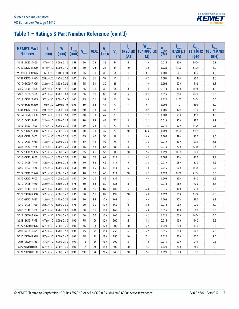
7© KEMET Electronics Corporation • P.O. Box 5928 • Greenville, SC 29606 • 864-963-6300 • www.kemet.com V0002_VC • 2/9/2017
Surface Mount VaristorsVC Series Low Voltage 125°C
Table 1 – Ratings & Part Number Reference (cont'd)
KEMET Part Number
L (mm)
W (mm)
tmax (mm) Vrms VDC Vn
1 mA Vc
Ic 8/20 µs
(A)
Wmax 10/1000 µs
(J)
Pmax (W)
Imax 8/20 µs
(A)
Ctyp at 1 kHz
(pF)
Ltyp 100 mA/ns
(nH)VC1812K801R020 4.7 ± 0.40 3.20 ± 0.30 1.55 20 26 33 54 5 3.0 0.015 800 3000 2.5
VC2220K122R020 5.7 ± 0.50 5.00 ± 0.40 1.45 20 26 33 54 10 8.0 0.020 1200 6500 3.0
VC0603K300R025 1.6 ± 0.20 0.80 ± 0.10 0.95 25 31 39 65 1 0.1 0.003 30 165 1.0
VC0805K121R025 2.0 ± 0.25 1.25 ± 0.20 1.05 25 31 39 65 1 0.2 0.005 120 260 1.5
VC1206K201R025 3.2 ± 0.30 1.60 ± 0.20 1.25 25 31 39 65 1 1.0 0.008 200 510 1.8
VC1210K401R025 3.2 ± 0.30 2.50 ± 0.25 1.45 25 31 39 65 3 1.8 0.010 400 1060 1.8
VC1812K801R025 4.7 ± 0.40 3.20 ± 0.30 1.55 25 31 39 65 5 3.9 0.015 800 2300 2.5
VC2220K122R025 5.7 ± 0.50 5.00 ± 0.40 1.45 25 31 39 65 10 9.5 0.020 1200 5000 3.0
VC0603K300R030 1.6 ± 0.20 0.80 ± 0.10 0.95 30 38 47 77 1 0.1 0.003 30 160 1.0
VC0805K121R030 2.0 ± 0.25 1.25 ± 0.20 1.05 30 38 47 77 1 0.2 0.005 120 230 1.5
VC1206K201R030 3.2 ± 0.30 1.60 ± 0.20 1.25 30 38 47 77 1 1.2 0.008 200 450 1.8
VC1210K301R030 3.2 ± 0.30 2.50 ± 0.25 1.45 30 38 47 77 3 2.1 0.010 300 850 1.8
VC1812K801R030 4.7 ± 0.40 3.20 ± 0.30 1.55 30 38 47 77 5 4.4 0.015 800 1800 2.5
VC2220K122R030 5.7 ± 0.50 5.00 ± 0.40 1.45 30 38 47 77 10 12.2 0.020 1200 4000 3.0
VC1206K121R035 3.2 ± 0.30 1.60 ± 0.20 1.25 35 45 56 90 1 0.6 0.008 120 400 1.8
VC1210K251R035 3.2 ± 0.30 2.50 ± 0.25 1.45 35 45 56 90 3 2.2 0.010 250 670 1.8
VC1812K601R035 4.7 ± 0.40 3.20 ± 0.30 1.55 35 45 56 90 5 4.2 0.015 600 1340 2.5
VC2220K102R035 5.7 ± 0.50 5.00 ± 0.40 1.45 35 45 56 90 10 7.6 0.020 1000 3000 3.0
VC1206K121R040 3.2 ± 0.30 1.60 ± 0.20 1.25 40 56 68 110 1 0.8 0.008 120 370 1.8
VC1210K251R040 3.2 ± 0.30 2.50 ± 0.25 1.45 40 56 68 110 3 2.4 0.010 250 570 1.8
VC1812K601R040 4.7 ± 0.40 3.20 ± 0.30 1.55 40 56 68 110 5 4.8 0.015 600 1000 2.5
VC2220K102R040 5.7 ± 0.50 5.00 ± 0.40 1.45 40 56 68 110 10 9.2 0.020 1000 2200 3.0
VC1206K121R050 3.2 ± 0.30 1.60 ± 0.20 1.65 50 65 82 135 1 0.8 0.008 120 340 1.8
VC1210K251R050 3.2 ± 0.30 2.50 ± 0.25 1.75 50 65 82 135 3 1.7 0.010 250 470 1.8
VC1812K401R050 4.7 ± 0.40 3.20 ± 0.30 1.85 50 65 82 135 5 4.8 0.015 400 710 2.5
VC2220K801R050 5.7 ± 0.50 5.00 ± 0.40 1.85 50 65 82 135 10 5.8 0.020 800 1500 3.0
VC1206K121R060 3.2 ± 0.30 1.60 ± 0.20 1.65 60 85 100 165 1 0.9 0.008 120 330 1.8
VC1210K251R060 3.2 ± 0.30 2.50 ± 0.25 1.75 60 85 100 165 3 2.2 0.010 250 390 1.8
VC1812K401R060 4.7 ± 0.40 3.20 ± 0.30 1.85 60 85 100 165 5 5.8 0.015 400 580 2.5
VC2220K801R060 5.7 ± 0.50 5.00 ± 0.40 1.85 60 85 100 165 10 6.2 0.020 800 1000 3.0
VC1812K401R075 4.7 ± 0.40 3.20 ± 0.30 1.90 75 100 120 200 5 5.8 0.015 400 440 2.5
VC2220K801R075 5.7 ± 0.50 5.00 ± 0.40 1.90 75 100 120 200 10 6.2 0.020 800 700 3.0
VC1812K301R095 4.7 ± 0.40 3.20 ± 0.30 1.90 95 125 150 250 5 5.2 0.015 300 340 2.5
VC2220K501R095 5.7 ± 0.50 5.00 ± 0.40 1.90 95 125 150 250 10 7.4 0.020 500 600 3.0
VC1812K301R115 4.7 ± 0.40 3.20 ± 0.30 1.90 115 150 180 300 5 5.2 0.015 300 310 2.5
VC2220K501R115 5.7 ± 0.50 5.00 ± 0.40 1.90 115 150 180 300 10 7.4 0.020 500 560 3.0
VC2220K501R130 5.7 ± 0.50 5.00 ± 0.40 1.90 130 170 205 340 10 7.4 0.020 500 500 3.0

8© KEMET Electronics Corporation • P.O. Box 5928 • Greenville, SC 29606 • 864-963-6300 • www.kemet.com V0002_VC • 2/9/2017
Surface Mount VaristorsVC Series Low Voltage 125°C
Soldering
PopularsolderingtechniquesusedforsurfacemountedcomponentsareWaveandInfraredReflowprocesses.Bothprocessescanbeperformed with Pb-containing or Pb-free solders. The termination option available for these soldering techniques is Barrier Type End Terminations.
End Termination Designation Recommended and Suitable for
Component RoHS Compliant
Ni Sn Barrier Type End Termination
Ni R1 Pb-containing and Pb-free soldering
Yes
Wave Soldering – this process is generally associated with discrete components mounted on the underside of printed circuit boards, or for large top-side components with bottom-side mounting tabs to be attached, such as the frames of transformers, relays, connectors, etc.SMDvaristorstobewavesolderedarefirstgluedtothecircuitboard,usuallywithanepoxyadhesive.WhenallcomponentsonthePCB have been positioned and an appropriate time is allowed for adhesive curing, the completed assembly is then placed on a conveyor and run through a single, double wave process.
Infrared Reflow Soldering–thesereflowprocessesaretypicallyassociatedwithtop-sidecomponentplacement.Thistechniqueutilizesamixtureofadhesiveandsoldercompounds(andsometimesfluxes)thatareblendedintoapaste.ThepasteisthenscreenedontoPCBsolderingpadsspecificallydesignedtoacceptaparticularsizedSMDcomponent.Therecommendedsolderpastewetlayerthicknessis100to300µm.OncethecircuitboardisfullypopulatedwithMDcomponents,itisplacedinareflowenvironment,wherethepasteisheatedtoslightlyaboveitseutectictemperature.Whenthesolderpastereflows,theSMDcomponentsareattachedtothesolderpads.
Solder Fluxes–solderfluxesaregenerallyappliedtopopulatedcircuitboardstocleanoxidesformingduringtheheatingprocessandtofacilitatetheflowingofthesolder.Solderfluxescanbeeitherapartofthesolderpastecompoundorcanbeseparatematerials,usuallyfluids.Recommendedfluxesare:
•non-activated(R)fluxes,wheneverpossible •mildlyactivated(RMA)fluxesofclassL3CN • class ORLO
Activated (RA),watersolubleorstrongacidicfluxeswithachlorinecontent>0.2wt.%areNOTRECOMMENDED.Theuseofsuchfluxescould create high leakage current paths along the body of the varistor components.Whenafluxisappliedpriortowavesoldering,itisimportanttocompletelydryanyresidualfluxsolventspriortothesolderingprocess.
Thermal Shock – to avoid the possibility of generating stresses in the varistor chip due to thermal shock, a preheat stage to within 100 °Cofthepeaksolderingprocesstemperatureisrecommended.Additionally,SMDvaristorsshouldnotbesubjectedtoatemperaturegradientgreaterthan4°C/sec.,withanidealgradientbeing2°C/sec.Peaktemperaturesshouldbecontrolled.WaveandReflowsolderingconditionsforSMDvaristorswithPb-containingsoldersareshowninFig.1and2respectively,whileWaveandReflowsolderingconditions for SMD varistors with Pb-free solders are shown in Fig, 1 and 3

9© KEMET Electronics Corporation • P.O. Box 5928 • Greenville, SC 29606 • 864-963-6300 • www.kemet.com V0002_VC • 2/9/2017
Surface Mount VaristorsVC Series Low Voltage 125°C
Soldering cont'd
WheneverseveraldifferenttypesofSMDcomponentsarebeingsoldered,eachhavingaspecificsolderingprofile,thesolderingprofilewith the least heat and the minimum amount of heating time is recommended. Once soldering has been completed, it is necessary to minimizethepossibilityofthermalshockbyallowingthehotPCBtocooltolessthan50°Cbeforecleaning.
Inspection Criteria–theinspectioncriteriatodetermineacceptablesolderjoints,whenWaveorInfraredReflowprocessesareused,willdependonseveralkeyvariables,principallyterminationmaterialprocessprofiles.
Pb-contining Wave and IR Reflow Soldering – typical “before” and “after” soldering results for Barrier Type End Terminations can be seen in Fig. 4. Barrier type terminated varistors form a reliable electrical contact and metallurgical bond between the end terminations and the solder pads. The bond between these two metallic surfaces is exceptionally strong and has been tested by both vertical pull and lateral (horizontal) push tests. The results exceed established industry standards for adhesion.
The solder joint appearance of a barrier type terminated varistor shows that solder forms a metallurgical junction with the thin tin-alloy (over the barrier layer), and due to its small volume “climbs” the outer surface of the terminations, the meniscus will be slightly lower. This optical appearance should be taken into consideration when programming visual inspection of the PCB after soldering.
Ni Sn Barrier Type End Terminations
Fig.4–SolderingCriterionincaseofWaveandIRReflowPb-containingSoldering
Pb-free Wave and IR Reflow Soldering – typical “before” and “after” soldering results for Barrier Type End Terminations are given in a phenomenon knows as “mirror” or “negative” meniscus. Solder forms a metallurgical junction with the entire volume of the end termination, i.e. it diffuses from pad to end termination across the inner side, forming a “mirror” or “negative” meniscus. The height of the solder penetration can be clearly seen on the end termination and is always 30% higher than the chip height.

10© KEMET Electronics Corporation • P.O. Box 5928 • Greenville, SC 29606 • 864-963-6300 • www.kemet.com V0002_VC • 2/9/2017
Surface Mount VaristorsVC Series Low Voltage 125°C
Soldering cont'd
Solder Test and Retained Samples–reflowsolderingtestbasedonJ-STD-020D.1andsolderingtestbydippingbasedonIEC60068-2 for Pb-free solders are preformed on each production lot as shown in the following chart. Test results and accompanying samples areretainedforaminimumoftwo(2)years.Thesolderabilityofaspecificlotcanbecheckedatanytimewithinthisperiodshouldacustomer require this information.
Test Resistance to Flux SolderabilityStatic leaching
(Simulation of Reflow Soldering)
Dynamic Leaching (Simulation of Wave
Soldering)Parameter
Soldering method dipping dipping dipping dipping with agitation
Flux L3CN, ORL0 L3CN, ORL0, R L3CN, ORL0, R L3CN, ORL0, R
Pb Solder 62Sn/36Pb/2 Ag
PbSolderingtemperature(°C) 235±5 235±5 260±5 235±5
Pb-FREE Solder Sn96/Cu0,4–0,8/3–4Ag
Pb-FREE Soldering Temperature(°C)
250±5 250±5 280±5 250±5
Soldering Time (s) 2 210 10 > 15
Burn-in Conditions VDCmax, 48 h
Acceptance Criterion dVn < 5 %, idc must stay unchanged
> 95 % of end termination must be covered by solder
> 95 % of end termination must be intact and covered
by solder
> 95 % of end termination must be intact and covered
by solder
Rework Criteria Soldering Iron – unless absolutely necessary, the use of soldering irons is NOT recommended for reworking varistor chips. If no other means of rework is available, the following criteria must be strictly followed:
• Do not allow the tip of the iron to directly contact the top of the chip•Donotexceedthefollowingsolderingironspecifications: Output Power: 30 Watts maximum TemperatureofSolderingIronTip: 280°Cmaximum Soldering Time: 10 Seconds maximum
Storage Conditions – SMD varistors should be used within 1 year of purchase to avoid possible soldering problems caused by oxidized terminals.Thestorageenvironmentshouldbecontrolled,withhumiditylessthan40%andtemperaturebetween-25and45°C.Varistorchips should always be stored in their original packaged unit.

11© KEMET Electronics Corporation • P.O. Box 5928 • Greenville, SC 29606 • 864-963-6300 • www.kemet.com V0002_VC • 2/9/2017
Surface Mount VaristorsVC Series Low Voltage 125°C
Soldering Pad Configuration
W
L
t
M
B C B
A
D
A
Size L (mm) W (mm) h (mm) tmax (mm) A (mm) B (mm) C (mm) D (mm)0603 1.6±0.20 0.80±0.10 0.5±0.25 1.0 1.0 1.0 0.6 2.6
0805 2.0±0.25 1.25±0.20 0.5±0.25 1.1 1.4 1.2 1.0 3.4
1206 3.2±0.30 1.60±0.20 0.5±0.25 1.6 1.8 1.2 2.1 4.5
1210 3.2±0.30 2.50±0.25 0.5±0.25 1.8 2.8 1.2 2.1 4.5
1812 4.7±0.40 3.20±0.30 0.5±0.25 1.9 3.6 1.5 3.2 6.2
2220 5.7±0.50 5.00±0.40 0.5±0.25 1.9 5.5 1.5 4.2 7.2
Packaging
Voltage Range (V)
Chip Size0603 0805 1206 1210 1812 2220
Reel Size180 180 180 180 180 180
2 to 14 4000 4000 4000 4000 1500 150017 3500 3500 2500 2500 1500 1500
20 to 40 3500 3500 2500 2500 1000 100050 to 130 2000 2000 1000 1000

12© KEMET Electronics Corporation • P.O. Box 5928 • Greenville, SC 29606 • 864-963-6300 • www.kemet.com V0002_VC • 2/9/2017
Surface Mount VaristorsVC Series Low Voltage 125°C
Construction
Glass Passivation
Detailed Cross Section
Inner Electrodes(Ag)
TerminateEdge
TerminateEdge
ZnO Layer
Inner Electrodes(Ag)
Glass Passivation
Termination(Ag/Pd, Ni/Sn)
Termination(Ag/Pd, Ni/Sn)

13© KEMET Electronics Corporation • P.O. Box 5928 • Greenville, SC 29606 • 864-963-6300 • www.kemet.com V0002_VC • 2/9/2017
Surface Mount VaristorsVC Series Low Voltage 125°C
Taping & Reel Specifications
Tape Size (mm) 8 mm 12 mm0603 0805 1206 1210 1812 2220
Ao 1.2 1.6 1.9 2.9 3.75 5.6Bo 1.9 2.4 3.75 3.7 5 6.25
Ko Maximum 1.1 1.1 1.8 2 2 2B1 Maximum 4.35 4.35 4.35 4.35 8.2 8.2D1 Minimum 0.3 0.3 0.3 0.3 1.5 1.5E2 Minimum 6.25 6.25 6.25 6.25 10.25 10.25
P1 4 4 4 4 8 8F 3.5 3.5 3.5 3.5 5.5 5.5W 8.0 8.0 8.0 8.0 12.0 12.0
T2 Maximum 3.5 3.5 3.5 3.5 6.5 6.5W1 8.4+1.5 8.4+1.5 8.4+1.5 8.4+1.5 12.4+2 12.4+2
W2 Maximum 14.4 14.4 14.4 14.4 18.4 18.4W3 7.9...10.9 7.9...10.9 7.9...10.9 7.9...10.9 11.9...15.4 11.9...15.4A 180 180 180 180 180 180

14© KEMET Electronics Corporation • P.O. Box 5928 • Greenville, SC 29606 • 864-963-6300 • www.kemet.com V0002_VC • 2/9/2017
Surface Mount VaristorsVC Series Low Voltage 125°C
Terms and Definitions
Term Symbol DefinitionRated AC Voltage Vrms
Maximum continuous sinusoidal AC voltage (<5% total harmonic distortion) which may be appliedtothecomponentundercontinuousoperationconditionsat25°C
Rated DC Voltage Vdc
Maximum continuous DC voltage (<5% ripple) which may be applied to the component under continuousoperatingconditionsat25°C
Supply Voltage V The voltage by which the system is designated and to which certain operating characteristics of
the system are referred; Vrms = 1,1 x V
Leakage Current IdcThecurrentpassingthroughthevaristoratVdcandat25°Coratanyotherspecified
temperatureVaristor Voltage Vn Voltage across the varistor measured at a given reference current In
Reference Current In Reference current = 1 mA DCClamping Voltage Protection Level Vc
The peak voltage developed across the varistor under standard atmospheric conditions, when passingan8/20μsclasscurrentpulse
Class Current IcA peak value of current which is 1/10 of the maximum peak current for 100 pulses at two per
minuteforthe8/20μspulseVoltage
Clamping Ratio
Vc/VappAfigureofmeritmeasureofthevaristorclampingeffectivenessasdefinedbythesymbols
Vc/Vapp, where (Vapp = Vrms or Vdc)
Jump Start
TransientVjump
The jump start transient resulting from the temporary application of an overvoltage in excess of the rated battery voltage. The circuit power supply may be subjected to a temporary
overvoltage condition due to the voltage regulation failing or it may be deliberately generated when it becomes necessary to boost start the car
Rated Single Pulse Transient Energy Wmax
Energywhichmaybedissipatedforasingle10/1000μspulseofamaximumratedcurrent, with rated AC voltage or rated DC voltage also applied, without causing device failure
Load Dump
TransientWLD
Load Dump is a transient which occurs in an automotive environment. It is an exponentially decaying positive voltage which occurs in the event of a battery disconect while the alternator is still generating charging current with other loads remaining on the alternator circuit at the
time of battery disconectRated Peak Single
Pulse Transient Current
ImaxMaximumpeakcurrentwhichmaybeappliedforasingle8/20μspulse,with,ratedline
voltage also applies, without causing device failure
Rated Transient Average Power
DissipationP Maximum average power which may be dissipated due to a group of pulses occurring within a
specifiedisolatedtimeperiod,withoutcausingdevicefailureat25°C
Capacitance C Capacitance between two terminals of the varistor measured at at 1 kHzResponse Time tr The time lag between application of a surge and varistor's "turn-on" conduction actionVaristor Voltage
Temperature Coefficient
TC (Vnat85°C–Vnat25°C)/(Vnat25°C)x60°C)x100
Insulation Resistance IR Minimum resistance between shorted terminals and varistor surfaceIsolation Voltage
The maximum peak voltage which may be applied under continuous operating conditions between the varistor terminations and any conducting mounting surface
Operating Temperature
The range of ambient temperature for which the varistor is designed to operate continuously as definedbythetemperaturelimitsofitsclimaticcategory
Climatic Category LCT/UCT/DHD
UCT = Upper Category Temperature – the maximum ambient temperature for which a varistor has been designed to operate continuously, LCT = Lower Category Temperature – the minimum
ambient temperature at which a varistor has been designed to operate continuously DHD = Dump Heat Test Duration
Storage Temperature Storage temperature range without voltage applied

15© KEMET Electronics Corporation • P.O. Box 5928 • Greenville, SC 29606 • 864-963-6300 • www.kemet.com V0002_VC • 2/9/2017
Surface Mount VaristorsVC Series Low Voltage 125°C
KEMET Electronic Corporation Sales Offi ces
Foracompletelistofourglobalsalesoffices,pleasevisitwww.kemet.com/sales.
DisclaimerAllproductspecifications,statements,informationanddata(collectively,the“Information”)inthisdatasheetaresubjecttochange.Thecustomerisresponsibleforchecking and verifying the extent to which the Information contained in this publication is applicable to an order at the time the order is placed.
All Information given herein is believed to be accurate and reliable, but it is presented without guarantee, warranty, or responsibility of any kind, expressed or implied.
Statements of suitability for certain applications are based on KEMET Electronics Corporation’s (“KEMET”) knowledge of typical operating conditions for such applications,butarenotintendedtoconstitute–andKEMETspecificallydisclaims–anywarrantyconcerningsuitabilityforaspecificcustomerapplicationoruse.The Information is intended for use only by customers who have the requisite experience and capability to determine the correct products for their application. Any technical advice inferred from this Information or otherwise provided by KEMET with reference to the use of KEMET’s products is given gratis, and KEMET assumes no obligation or liability for the advice given or results obtained.
Although KEMET designs and manufactures its products to the most stringent quality and safety standards, given the current state of the art, isolated component failures may still occur. Accordingly, customer applications which require a high degree of reliability or safety should employ suitable designs or other safeguards (such as installation of protective circuitry or redundancies) in order to ensure that the failure of an electrical component does not result in a risk of personal injury or property damage.
Although all product–related warnings, cautions and notes must be observed, the customer should not assume that all safety measures are indicted or that other measures may not be required.
KEMET is a registered trademark of KEMET Electronics Corporation.