surface & coatings technology - university of nottingham · 1396 j.f. li et al. / surface &...
TRANSCRIPT
Surface & Coatings Technology 204 (2010) 1395–1404
Contents lists available at ScienceDirect
Surface & Coatings Technology
j ourna l homepage: www.e lsev ie r.com/ locate /sur fcoat
Characterization and solderability of cold sprayed Sn–Cu coatings onAl and Cu substrates
J.F. Li a,⁎, P.A. Agyakwa a, C.M. Johnson a, D. Zhang b, T. Hussain b, D.G. McCartney b
a Department of Electrical and Electronic Engineering, The University of Nottingham, University Park, Nottingham NG7 2RD, United Kingdomb Department of Mechanical, Materials and Manufacturing Engineering, The University of Nottingham, University Park, Nottingham NG7 2RD, United Kingdom
⁎ Corresponding author.E-mail address: [email protected] (J.F. Li).
0257-8972/$ – see front matter © 2009 Elsevier B.V. Aldoi:10.1016/j.surfcoat.2009.09.025
a b s t r a c t
a r t i c l e i n f oArticle history:Received 5 August 2009Accepted in revised form 9 September 2009Available online 17 September 2009
Keywords:RoughnessPhotoelectron spectroscopyTransmission electron microscopy (TEM)TinTin oxideCold spraying
Cold sprayed Sn–Cu coatings approximately 40 and 25 μm in average thickness were deposited onaluminium and direct bonded copper (DBC) substrates respectively. Both a statistical analysis of coatingthickness and a roughness analysis of the coating/substrate interface and the coating surface were carriedout for the as-sprayed coatings using scanning electron microscope images. The results obtained can berelated to substrate types and spraying conditions. Tin oxide on the surfaces of the as-sprayed coatings wasrevealed by employing X-ray photoelectron spectroscopy analyses and transmission electron microscopy. Itcame from an oxide shell around feedstock powder particles and was only locally broken down during coldspraying. Although the tin oxide inhibited fluxless soldering, flux-supported reflow of cold sprayed Sn on theDBC substrate produced Cu/Sn/Cu solder joints that were acceptable for application in electronic packagingand interconnects. In general, measures which can avoid or remove the tin oxide are needed to achieveimproved solder joints using cold sprayed Sn coatings as the solder layers.
l rights reserved.
© 2009 Elsevier B.V. All rights reserved.
1. Introduction
Cold gas dynamic spraying, commonly referred to as cold spray,was developed in the mid 1980s at the Institute of Theoretical andApplied Mechanics of the Siberian Division of the Russian Academy ofScience in Novosibirsk [1,2]. During cold spray, powder particles,usually in the size range of 1 to 50 µm, are accelerated through a deLaval type of converging–diverging nozzle by a supersonic gas flow.Typically particle speeds of 300 to 1200 m/s are attained and thepowder particles are directed to impact on a substrate or previouslydeposited powder to form a coherent coating. Heated air or nitrogenmay be used as the accelerating gas but the best quality of coatings isgenerally achieved by using helium at room, or slightly elevated,temperature [2,3]. Al and Cu coatings deposited by cold spray havebeen the most extensively investigated to date. Studies have includedoptimization of the spraying process, the bonding mechanism,microstructure formation and the thermal stability of the deposits[3–9]. A number of othermetallic materials have also been reported tobe successfully deposited by cold spray to produce coatings, includingSn, Al–Sn and Cu–Sn as examples relevant to the present work [10–14].
Cold sprayed coatings are reported to have relatively low porosityand a low oxygen or oxide content [14,15]. As a result, cold spray hasbeen investigated as a method to produce solderable surfaces on
materials with poor wettability (e.g. heat sinks, such as Cu on Al) andto deposit brazing and soldering alloys for applications in electronicpackaging and interconnects [15,16]. For example, a cold sprayed Cucoating on a heat sinkmade of Al as a base layer has been successful asa solderable surface for the Sn- or Cu-plated area of electronic devices[15]. In this case, the high kinetic energy of the Cu particles wassufficient to break up the oxide film on the aluminium surface. Forsimilar electronic applications, cold sprayed Al coatings might also beused as bonding layers, e.g. onto a hard and brittle Al2O3 substrate, fordepositing other top layers, such as Cu and Sn, using another coating/film process [15].
Another interesting effort in the field of cold spray was thedeposition of conducting layers onto plastics [16]. By controlling thespraying process conditions, it was possible to deposit Cu onto PA 66(nylon 6/6), but the bond strength between the Cu deposit and thesubstrate appeared to be rather low.
Cold spray has been investigated for depositing Sn-based solderalloy layers although substrate types were not reported [15]. Also theeffects of substrate temperature and gun transverse speed on theformation mechanism of cold sprayed Sn coatings were alsosystematically studied by Legoux et al. [11]. Although a depositionefficiency of less than 5% was reported for Sn coatings on a steelsubstrate, scanning electron microscopy images of the polished crosssections indicate that a continuous solder layer with a thickness of 20to 30 µm and a surface roughness, Ra, of 1–20 µm could be achieved,see Fig. 13 in [11].
In addition, cold spray was used to deposit Zn–Al–Si brazing alloysfor joining Al or Al-based alloys [17]. In this case, the cold spray process
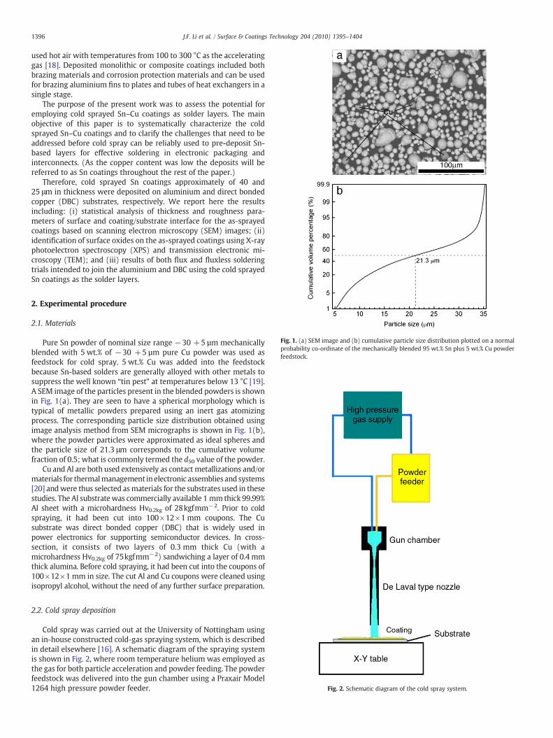
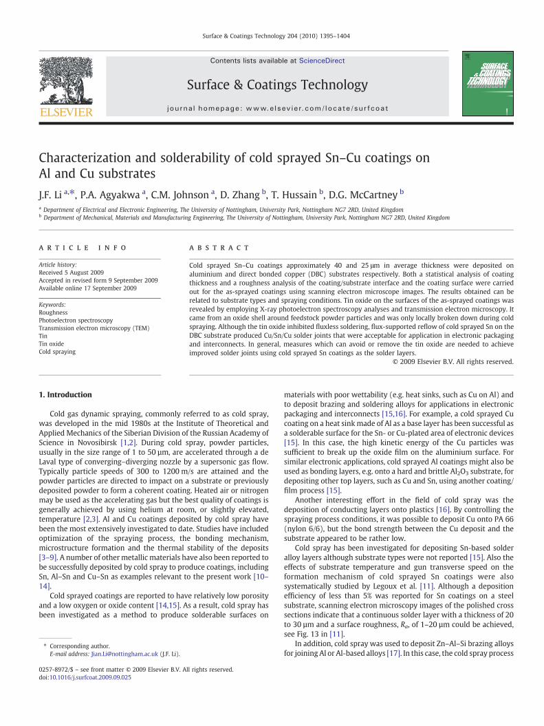
Fig. 1. (a) SEM image and (b) cumulative particle size distribution plotted on a normalprobability co-ordinate of the mechanically blended 95 wt.% Sn plus 5 wt.% Cu powderfeedstock.
Fig. 2. Schematic diagram of the cold spray system.
1396 J.F. Li et al. / Surface & Coatings Technology 204 (2010) 1395–1404
used hot air with temperatures from 100 to 300 °C as the acceleratinggas [18]. Deposited monolithic or composite coatings included bothbrazing materials and corrosion protection materials and can be usedfor brazing aluminium fins to plates and tubes of heat exchangers in asingle stage.
The purpose of the present work was to assess the potential foremploying cold sprayed Sn–Cu coatings as solder layers. The mainobjective of this paper is to systematically characterize the coldsprayed Sn–Cu coatings and to clarify the challenges that need to beaddressed before cold spray can be reliably used to pre-deposit Sn-based layers for effective soldering in electronic packaging andinterconnects. (As the copper content was low the deposits will bereferred to as Sn coatings throughout the rest of the paper.)
Therefore, cold sprayed Sn coatings approximately of 40 and25 μm in thickness were deposited on aluminium and direct bondedcopper (DBC) substrates, respectively. We report here the resultsincluding: (i) statistical analysis of thickness and roughness para-meters of surface and coating/substrate interface for the as-sprayedcoatings based on scanning electron microscopy (SEM) images; (ii)identification of surface oxides on the as-sprayed coatings using X-rayphotoelectron spectroscopy (XPS) and transmission electronic mi-croscopy (TEM); and (iii) results of both flux and fluxless solderingtrials intended to join the aluminium and DBC using the cold sprayedSn coatings as the solder layers.
2. Experimental procedure
2.1. Materials
Pure Sn powder of nominal size range −30 +5 µm mechanicallyblended with 5 wt.% of −30 +5 µm pure Cu powder was used asfeedstock for cold spray. 5 wt.% Cu was added into the feedstockbecause Sn-based solders are generally alloyed with other metals tosuppress the well known “tin pest” at temperatures below 13 °C [19].A SEM image of the particles present in the blended powders is shownin Fig. 1(a). They are seen to have a spherical morphology which istypical of metallic powders prepared using an inert gas atomizingprocess. The corresponding particle size distribution obtained usingimage analysis method from SEM micrographs is shown in Fig. 1(b),where the powder particles were approximated as ideal spheres andthe particle size of 21.3 μm corresponds to the cumulative volumefraction of 0.5; what is commonly termed the d50 value of the powder.
Cu and Al are both used extensively as contact metallizations and/ormaterials for thermalmanagement inelectronic assemblies and systems[20] andwere thus selected asmaterials for the substrates used in thesestudies. The Al substratewas commercially available 1 mm thick 99.99%Al sheet with a microhardness Hv0.2kg of 28kgfmm−2. Prior to coldspraying, it had been cut into 100×12×1 mm coupons. The Cusubstrate was direct bonded copper (DBC) that is widely used inpower electronics for supporting semiconductor devices. In cross-section, it consists of two layers of 0.3 mm thick Cu (with amicrohardness Hv0.2kg of 75kgfmm−2) sandwiching a layer of 0.4 mmthick alumina. Before cold spraying, it had been cut into the coupons of100×12×1 mm in size. The cut Al and Cu coupons were cleaned usingisopropyl alcohol, without the need of any further surface preparation.
2.2. Cold spray deposition
Cold spray was carried out at the University of Nottingham usingan in-house constructed cold-gas spraying system, which is describedin detail elsewhere [16]. A schematic diagram of the spraying systemis shown in Fig. 2, where room temperature helium was employed asthe gas for both particle acceleration and powder feeding. The powderfeedstock was delivered into the gun chamber using a Praxair Model1264 high pressure powder feeder.

Table 1Sample codes and the main processing parameters of the cold sprayed Sn–Cu coatings.
Sample code AA1 AA2 AC1
Substrate Al Al DBCHe pressure (MPa) 1.0 2.0 1.0Powder feed rate (g/min) 15 15 15Standoff distance (mm) 20 20 20Gun traverse speed (mm/s) 100 100 100
1397J.F. Li et al. / Surface & Coatings Technology 204 (2010) 1395–1404
Following initial trials, two sets of processing parameters wereemployed to spray the feedstock of blended Sn–Cu powder particles.Sample codes and the corresponding processing parameters are listedin Table 1. In all cases, the pressure of the powder carrier gas was0.1 MPa above that of the main accelerating gas. All three coatingswere produced in a single pass because multiple passes were found tolead to de-bonding of the coatings from the substrates. The standalone de-bonded coatings produced by two passes were somewhatthicker (100–150 µm) than the coatings prepared using a singlespraying pass which were typically 25–40 µm thick.
2.3. Soldering trials
As reported below, the coating coded AA2was discontinuous. Thusonly the as-sprayed AA1 and AC1 coatings were cut into pieces of12×10×1 mm and 15×12×1 mm respectively for soldering experi-ments. The soldering experiments were carried out using the samplegeometries shown in Fig. 3. Because of the deformation of the Alsubstrate caused during cutting, a layer of 50 μm eutectic Sn–Ag foilwas inserted in the middle to improve the gap filling for the AA1coating, Fig. 3(a). Before the soldering processes, all samples wereultrasonically cleaned using isopropyl alcohol (IPA), rinsed usingacetone and deionised water. For purposes of comparison, threereflow processes termed RP1, RP2 and RP3 were employed and arelisted in Table 2. Theywere used for both the Al/Sn–SnAg–Sn/Al (AA1)and DBC/Sn–Sn/DBC (AC1) systems.
Of the three reflow processes listed in Table 2, RP1 and RP2 aretypical of a fluxless soldering process that might be applied in theassembly of power electronic modules either for die or substratemount down. Such processes typically involve the use of solder foilpre-forms normally between 100 and 400μm in thickness. Forminggas is used to clean the surfaces and a vacuum is used to reducevoiding. This process is preferred for making large area (N100 mm2)bonds. Surface abrading used in RP2 is to see whether this couldeffectively remove surface oxide on the coatings. RP3 is typical of thefluxed solder reflow process that is widely used in electronics
Fig. 3. Schematic sample geometries for the soldering experiments: (a)
assembly. Here a pre-fluxed solder paste is employed and reflowtakes place in an ambient air environment.
2.4. Coating and solder joint characterization using scanning electronmicroscopy (SEM)
A JEOL 6400 SEM was used to examine as-sprayed coating topsurfaces and cross-sections of coating microstructures using second-ary electron (SE) and backscattered electron (BSE) imaging.
Metallographic cross-sections of the coatings were prepared forthickness and roughness measurements using the following proce-dure. The coating samples were first cut into pieces approximately15×5×1 mm and then mounted in epoxy resin that was cured atroom temperature for 24h. The mounted samples were thensuccessively ground with 400, 800, 1000, 1200 and 2400 grit SiCpapers and finally polished using diamond slurries of 3 μm and 1 μmfor 10 min and 5 min, respectively.
The image analysis method used to extract the original substrate/surface, coating/surface and coating/substrate interfacial profiles fromthe cross-sectional SEM images utilized the Image Processing ToolboxVersion 5.0.0 of MATLAB R14SP2 (Mathworks) and is shown schema-tically in Fig. 4. For each sample, three to five images at a resolution of512×416pixels and an image size of 1175×940 μm were used andthe obtained data were merged together. Fig. 4(a) shows a SEM imageand Fig. 4(b) reveals the extracted profiles. The thickness of a coatingsample can be expressed, in principle, as a function of location x alongthe coating by:
tðxÞ = ztðxÞ−zbðxÞ; x∈½0; L0� ð1Þ
where t(x) is the thickness, L0 is the cross-sectional length of theprofiles, zt(x) and zb(x) are the vertical coordinates of the profiles ofthe coating surface and the coating/substrate interface, respectively,see Fig. 4(c). The captured digital SEM images were used to generatedata sets and so Eq. (1) takes on a discrete form:
ti = ztðxiÞ−zbðxiÞ; i = 1;2; ::;n ð2Þ
where n is the total number of data points. Then the mean, standarddeviation, minimum and maximum values of the thickness data canbe calculated as detailed in [21,22]. In addition, the cumulativeprobability for the resulting thickness data, f (tj), could be obtainedfrom placing the data in ascending order and letting
f ðtjÞ =j−0:5
n; j = 1;2; ::; n ð3Þ
Al/Sn–SnAg–Sn/Al (AA1) and (b) DBC/Sn–Sn/DBC (AC1) systems.
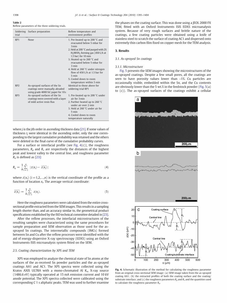
Table 2Reflow parameters of the three soldering trials.
Solderingtrial
Surface preparation Reflow temperature andenvironment profiles
RP1 None 1. Pre-heated up to 200 °C andevacuated below 5 mbar for3min
2. Held at 200 °C andpurgedwith2%H298%N2 forming gas (450 L/h at1.5 bar) for 10 min
3. Heated up to 260 °C andevacuated below 5 mbar for3 min
4. Held at 260 °C under nitrogenflow of 450 L/h at 1.5 bar for5 min
5. Cooled down to roomtemperature within 5 min
RP2 As-sprayed surfaces of the Sncoatings were manually abradedusing grade 4000 SiC paper for 10s
Identical to those above forsoldering trial RP1
RP3 As-sprayed surfaces of the Sncoatings were covered with a layerof mild active resin flux
1. Pre-heated up to 200 °C underair for 3min
2. Further heated up to 260 °Cunder air over 2 min
3. Held at 260 °C under air for5 min
4. Cooled down to roomtemperature naturally
Fig. 4. Schematic illustration of the method for calculating the roughness parameterfrom an original cross-sectional SEM image: (a) SEM image taken from the as-sprayedcoating AA1; (b) the extracted profiles of both the coating surface and the coating/substrate interface; and (c) the roughness parameters Rp and Rv and the quantities usedto calculate the roughness parameter Ra.
1398 J.F. Li et al. / Surface & Coatings Technology 204 (2010) 1395–1404
where j is the jth order in ascending thickness data [21]. If some values ofthickness tj were identical in the ascending order, only the one corres-ponding to the largest cumulativeprobabilitywas retainedand theotherswere deleted in the final curve of the cumulative probability curves.
For a surface or interfacial profile (see Fig. 4(c)), the roughnessparameters, Rp and Rv are respectively the distances of the highestpeak and lowest valley to the central line, and roughness parameterRa is defined as [23]:
Ra =1n∑n
i=1jzðxiÞ− zðxiÞ
P j ð4Þ
where z(xi) (i=1,2,…,n) is the vertical coordinate of the profile as afunction of location xi. The average vertical coordinate:
zðxiÞP
=1n∑n
i=1zðxiÞ: ð5Þ
Here the roughness parameterswere calculated from the entire cross-sectional profile extracted fromtheSEMimages. This results in a samplinglength shorter than, and an accuracy similar to, the geometrical productspecifications established by the ISO technical committee detailed in [23].
After the reflow processes, the interfacial microstructures of theresulting samples were characterized using the same procedures forsample preparation and SEM observation as those used for the as-sprayed Sn coatings. The intermetallic compounds (IMCs) formedbetween Sn and Cu after the reflow processes were identifiedwith theaid of energy-dispersive X-ray spectroscopy (EDXS) using an OxfordInstruments ISIS microanalysis system fitted on the SEM.
2.5. Coating characterization by XPS and TEM
XPS was employed to analyze the chemical state of Sn atoms at thesurfaces of the as-received Sn powder particles and the as-sprayedcoatings AA1 and AC1. The XPS spectra were collected using theKratos AXIS ULTRA with a mono-chromated Al Kα X-ray source(1486.6 eV) typically operated at 15 mA emission current and 10 kVanode potential. The XPS spectra collected were calibrated using thecorresponding C 1 s aliphatic peaks. TEMwas used to further examine
the phases on the coating surface. This was done using a JEOL 2000 FXTEM, fitted with an Oxford Instruments ISIS EDXS microanalysissystem. Because of very rough surfaces and brittle nature of thecoatings, a few coating particles were obtained using a knife ofstainless steel to scratch the surface of coating AC1 and dispersed ontoextremely thin carbon film fixed on coppermesh for the TEM analysis.
3. Results
3.1. As-sprayed Sn coatings
3.1.1. MicrostructureFig. 5 presents the SEM images showing the microstructures of the
as-sprayed coatings. Despite a few small pores, all the coatings areseen to have porosity values lower than ~1%. Cu particles areoccasionally visible, embedded within the Sn, and the Cu contentsare obviously lower than the 5 wt.% in the feedstock powder (Fig. 5(a)to (c)). The as-sprayed surfaces of the coatings exhibit a cellular
Fig. 5. SEM images of the three as-sprayed Sn coatings: (a) AA1, polished cross section; (b) AA2, polished cross section; (c) AC1, polished cross section; and (d) AC1, as-sprayedsurface.
1399J.F. Li et al. / Surface & Coatings Technology 204 (2010) 1395–1404
morphology of particles that were impacted and bonded on thepreviously deposited particles (Fig. 5d). However, the flattening of theparticles was rather limited.
Using the lower pressure (1.0 MPa) for the helium gas, continuouscoatings AA1 and AC1were achieved on both the Al and Cu substrates.Both the surface and coating/substrate interface profiles are ratherrough, and the surface profiles are apparently rougher than thecoating/substrate interface profiles (Fig. 5(a) and (c)). Comparing thecoatings on the two substrates, the coating AA1 on the Al substrate isthicker, and has a less rough surface but more irregular coating/substrate interface than the coating AC1 on Cu substrate.
Fig. 6. Cumulative probability curves of the thickness variations of the three as-sprayedcoatings on normal probability coordinates.
Using a higher pressure (2.0 MPa) for the helium gas, the majorityof the Sn particles were found to penetrate into the Al substrate moresignificantly than with coating AA1 and the resulting coating AA2 wasdiscontinuous (Fig. 5(b)). The coating/substrate interface becamerougher and has similar irregularity to the surface.
No metallurgical interfacial reaction (involving formation of a newphase) was detected and hence a solid state bond has apparentlyformed between the coatings and the substrates. Craters that wereproduced due to the high-velocity impact of the initial Sn particles hadenhanced the bonding of the deformed Sn particles to the substrates
Table 3Results of thickness measurement and surface roughness analysis of the as-sprayed Sn–Cu coatings.
Sample code AA1 AA2 AC1
Coating thickness Mean (μm) 39.7 35.7 25.1S.D. (μm) 7.8 11.4 9.1tmin (μm) 16.1 0.0 4.6tmax (μm) 64.5 69.8 48.8
Coating surface Ra (μm) 5.2 5.7 6.9Rp (μm) 23.8 21.9 24.5Rv (μm) 20.1 15.4 17.5
Coating/substrate interface Ra (μm) 4.9 6.3 2.6Rp (μm) 18.1 20.1 8.0Rv (μm) 15.6 21.8 9.6
Original substrate surface Ra (μm) 2.3 2.3 1.3Rp (μm) 7.8 7.8 3.6Rv (μm) 9.1 9.1 2.9

Fig. 7. Sn 3d XPS spectra for the as-received Sn powder and the as-sprayed coatings AA1and AC1. ASn
4+ and ASn0 represent the areas of the peaks corresponding to Sn4+ and Sn0
states.
1400 J.F. Li et al. / Surface & Coatings Technology 204 (2010) 1395–1404
and produced the irregular profiles of the coating/substrate interfaces(Fig. 5).
3.1.2. Statistical analysis of coating thicknessThe data obtained from the coating thickness measurements using
image analysis were analyzed as described in this section. Fig. 6presents cumulative probability curves of thicknesses variations of thethree as-sprayed coatings plotted on normal probability coordinates,where the vertical axis is in the probability scale representing theinverse of a cumulative Gaussian distribution as expressed as:
Φ−1½FðtÞ� = − μσ
+1σt ð7Þ
where μ is the mean, σ is the standard deviation and F(t) is thecumulative Gaussian function:
FðtÞ = 1σ
ffiffiffiffiffiffi2π
p ∫t
−∞exp
t−μ2σ2
� �dt: ð8Þ
Therefore, for data following an ideal normal distribution, thecumulative probability curve would be a straight line on the normalprobability coordinates. As shown in Fig. 6, this is the case for thethickness variations of all the three as-sprayed coatings.
Among the three coatings, a lower slope indicates that thethickness of coating AA2 on Al substrate produced using a higherpressure (2.0 MPa) for the He gas shows more variability than that ofthe coating AA1 on the Al substrate which was produced with a lowerhelium gas pressure (1.0 MPa). The coating AC1 on Cu substrate isseen to be thinner than, but has uniformity similar to, that of coatingAA1. The latter can be seen from their cumulative probability curveswhich are approximately parallel to one another.
The characteristic parameters of the normal distribution, includingthe mean and standard deviation, together with the minimum andmaximum values of the thickness of the three as-sprayed coatings arelisted in Table 3. It can be further seen that the average thickness, i.e.themean of coating AA2 is slightly less than that of coating AA1. All thethree coatings have maximum thicknesses that are obviously greaterthan the diameter of the largest particle in the feedstock powder. Inaddition, based on the known powder feed rate, gun traverse speedand step width, the deposition efficiencies for production of the threecoatingswere calculated from the average thicknesses listed in Table 3.In this calculation, pores within the coatings were ignored and thedensity of Sn was taken as 7287kgm−3 for both the powder particlesand the coatings. The calculated deposition efficiencies are 46%, 42%and 29% for the coatings AA1, AA2 and AC1, respectively.
3.1.3. Roughness analysisThe results of the roughness measurements for the coating surface,
the coating/substrate interface and the original substrate surface of
the three coatings are also listed in Table 3. Compared with theoriginal substrate surfaces, the coating/substrate interfaces are seen tobe coarsened with significantly increased roughness parameters. Thisis because the interfaces consist of craters produced by high-velocityimpacting Sn particles during the initial deposition stage. It is thuseasily understood that the coating/Al interfaces are more irregularthan the coating/Cu interface because the Al substrate is somewhatsofter than the Cu substrate. It is interesting to note that the roughnessparameters of the coating/Al interface are increased when thepressure of the helium gas was doubled.
3.1.4. Surface analysisXPS spectra can be used to analyze the chemical states of a few
layers of atoms at the surface of a material. As shown in Fig. 7,obtained from Sn powder and coating top surfaces, the weak peaks at484.4 eV for the Sn 3d XPS binding energy correspond to the Sn atomsin the form of metallic tin (Sn0), while the dominant peaks at 484.4 eVcorrespond to those of tin oxide (Sn4+) [24]. From the ratio of peakarea for Sn4+ to that for Sn0, it can be seen that the surfaces of the as-received Sn powder particles are covered with an oxide shell. Thislayer of oxide might be formed during the manufacturing process ortransportation and storage of the Sn powder. After cold spraying, theoxide shell had apparently been broken down locally to exposemetallic Sn atoms on the coating surfaces, as reflected by theincreased intensities of the XPS peaks for Sn0. However, the exposureof fresh Sn atoms is limited and the as-sprayed coating surfaces werestill predominately covered by the tin oxide.
Fig. 8 displays the results of TEM analysis of the particles removedfrom the top surface of coating AC1. Fig. 8(a) and (d) are TEM imagesof separate polycrystalline particles. Fig. 8(b) and (e) are therespective selected area electron diffraction (ED) patterns. Thediscrete spots on Fig. 8(b) correspond to the interplanar spacingswhich are consistent with those of SnO2. The rings drawn on Fig. 8(b)are the patterns which would be produced by a polycrystalline SnO2
sample. In Fig. 8(e), a number of discrete diffraction spots are visible.Also drawn on Fig. 8(e) are the rings which would be produced by apolycrystalline Sn sample and also a [3̄31 ̄] zone axis pattern for Sn.Therefore, the corresponding selected areas in Fig. 8(a) and (d) areSnO2 and Sn respectively. This is confirmed by the EDXS spectra inFig. 8(c) and (f), where a more pronounced oxygen peak is seen inFig. 8(c). Note that the minimum electron beam spot size achievablefor the EDXS analysis was approximately 200 nm, and some Cu camefrom the supporting Cu mesh for the sample. Because of thedestructive nature of TEM sample preparation, it is difficult to obtainthe images directly reflecting the distribution of the SnO2 layer on thecoating surface. Nevertheless, from the size of the SnO2 grains, it canbe reasonably deduced that the oxide shell on the as-received Snpowder particles, and hence the oxide layer covering most surfaces ofthe as-sprayed coatings, is a few to ten nm in thickness.
3.2. Soldering
3.2.1. Sn coating on Al substrate — coating AA1After reflow process RP1 under nitrogen, the Sn coating was still
mechanically bonded to the Al substrate. However, the coating failedto bond to the eutectic SnAg solder foil between the substrates (seeFig. 3 for schematic of the process). Fig. 9(a) shows that the surface ofthe coating still has a roughness profile similar to the as-sprayedsurface. These reflow results indicate that the thin layer of tin oxide onthe coating surface is very tenacious. Only a very small part of themolten Sn could have flowed out of the locally fresh surface into theSnAg solder to slightly reduce the average thickness of the coatingfrom 40 to 38 µm.
When the as-sprayed surface of the Sn coating was first manuallyabraded using grade 4000 SiC paper for 10s, the Sn coating on the twosides of the Al/Sn–SnAg–Sn/Al sample could be partially joined to the

Fig. 8. TEM results of particles removed from the surface of coating AC1: (a) TEM image of one Sn particle; (b) selected area ED spots distributed along the diffraction rings drawn forSnO2; (c) EDXS spectrum showing strong Sn peaks but with evidence for the presence of O around the selected area; d) TEM image of another Sn particle; (e) selected area ED spotsof zone [3̄31 ̄] or distributed along the diffraction rings drawn for Sn; and (f) EDXS spectrum showing strong Sn peaks and lower O content around this selected area.
1401J.F. Li et al. / Surface & Coatings Technology 204 (2010) 1395–1404
eutectic SnAg solder foil following the reflow process RP2. Theeffective bonding areas on both sides occupy approximately 40% ofthe total contact area between the Sn coating and the SnAg solder foilas seen in Fig. 9(b). Some voids still remain between the Sn coatingand the SnAg solder foil. They are probably associated with the tinoxide left at the valleys of the rough coating surface followingabrading with SiC.
After the flux reflow process RP3 (carried out in air), the Sn coatinghad de-bonded from the Al substrate, Fig. 9(c). This can be understoodbecause Al reacts rapidly with oxygen in air to form a thin oxide scale.Although the flux was successful in removing the tin oxide from theSn coating surface, it failed to prevent the Al substrate forming this
thin layer of oxide on its surface. As a result of the gradual spreading ofthe alumina along the coating/Al interface, the molten Sn wasdisplaced from the Al substrate. Most of the molten Sn coatingcoalesced with the molten SnAg solder (not visible in Fig. 9(c)). A fewnon-wetting isolated Sn droplets remain attached to the roughenedsurface of the Al substrate (previously the coating/Al interface).
3.2.2. Sn coating on Cu substrate — coating AC1After reflow process RP1 under nitrogen, the Sn coatings on the
two sides of the DBC/Sn–Sn/DBC samplewere not joined together (seeFig. 3(b) for schematic of process). Again, this can be attributed to tinoxide on the coating surface. Intermetallic compounds (IMCs),
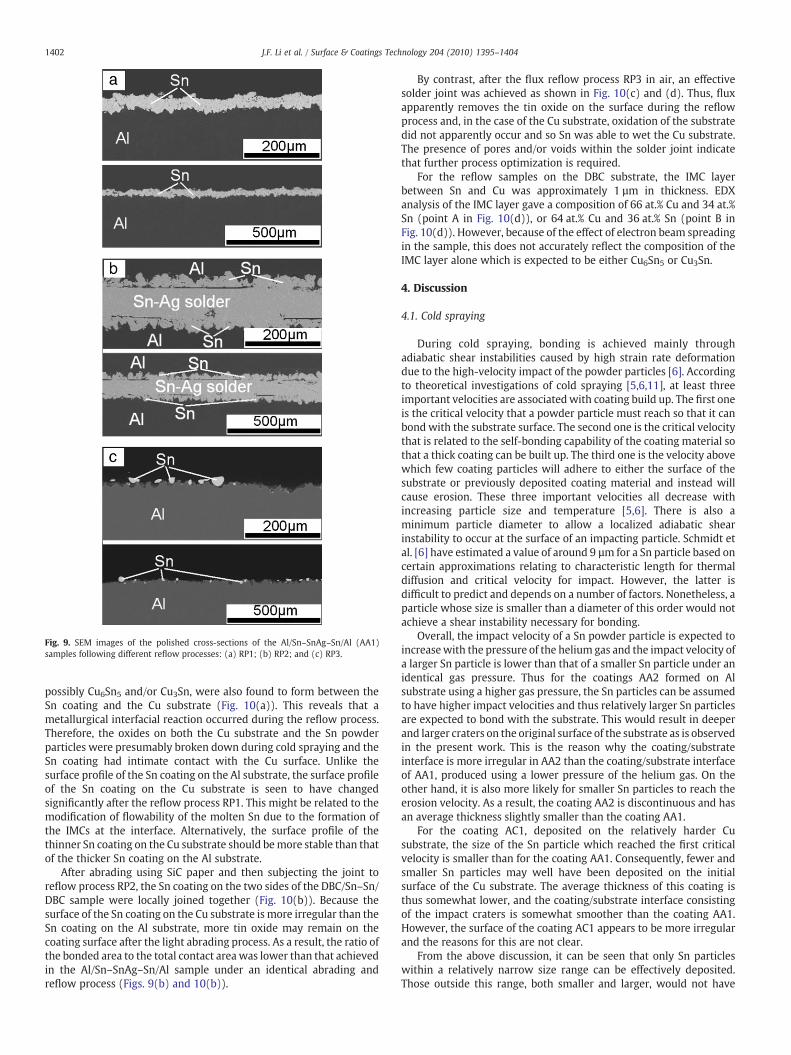
Fig. 9. SEM images of the polished cross-sections of the Al/Sn–SnAg–Sn/Al (AA1)samples following different reflow processes: (a) RP1; (b) RP2; and (c) RP3.
1402 J.F. Li et al. / Surface & Coatings Technology 204 (2010) 1395–1404
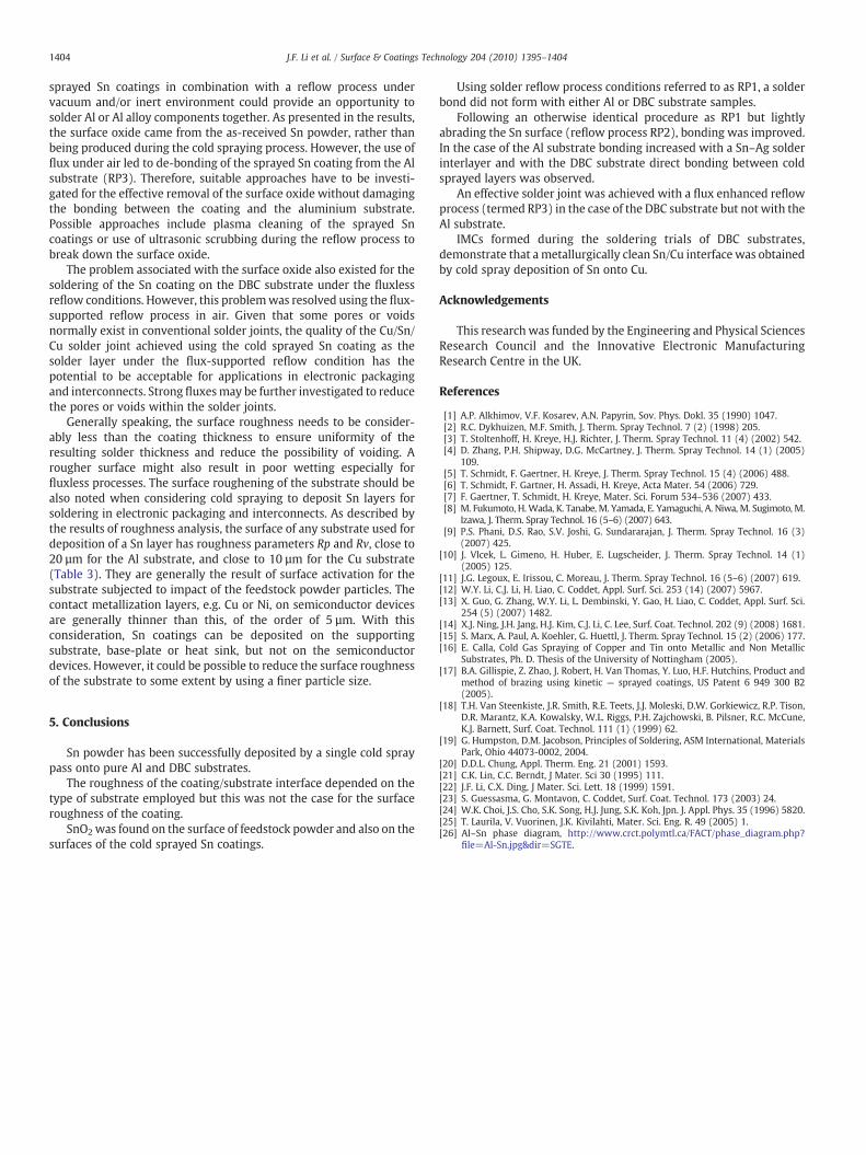
possibly Cu6Sn5 and/or Cu3Sn, were also found to form between theSn coating and the Cu substrate (Fig. 10(a)). This reveals that ametallurgical interfacial reaction occurred during the reflow process.Therefore, the oxides on both the Cu substrate and the Sn powderparticles were presumably broken down during cold spraying and theSn coating had intimate contact with the Cu surface. Unlike thesurface profile of the Sn coating on the Al substrate, the surface profileof the Sn coating on the Cu substrate is seen to have changedsignificantly after the reflow process RP1. This might be related to themodification of flowability of the molten Sn due to the formation ofthe IMCs at the interface. Alternatively, the surface profile of thethinner Sn coating on the Cu substrate should bemore stable than thatof the thicker Sn coating on the Al substrate.
After abrading using SiC paper and then subjecting the joint toreflow process RP2, the Sn coating on the two sides of the DBC/Sn–Sn/DBC sample were locally joined together (Fig. 10(b)). Because thesurface of the Sn coating on the Cu substrate is more irregular than theSn coating on the Al substrate, more tin oxide may remain on thecoating surface after the light abrading process. As a result, the ratio ofthe bonded area to the total contact area was lower than that achievedin the Al/Sn–SnAg–Sn/Al sample under an identical abrading andreflow process (Figs. 9(b) and 10(b)).
By contrast, after the flux reflow process RP3 in air, an effectivesolder joint was achieved as shown in Fig. 10(c) and (d). Thus, fluxapparently removes the tin oxide on the surface during the reflowprocess and, in the case of the Cu substrate, oxidation of the substratedid not apparently occur and so Sn was able to wet the Cu substrate.The presence of pores and/or voids within the solder joint indicatethat further process optimization is required.
For the reflow samples on the DBC substrate, the IMC layerbetween Sn and Cu was approximately 1 µm in thickness. EDXanalysis of the IMC layer gave a composition of 66 at.% Cu and 34 at.%Sn (point A in Fig. 10(d)), or 64 at.% Cu and 36 at.% Sn (point B inFig. 10(d)). However, because of the effect of electron beam spreadingin the sample, this does not accurately reflect the composition of theIMC layer alone which is expected to be either Cu6Sn5 or Cu3Sn.
4. Discussion
4.1. Cold spraying
During cold spraying, bonding is achieved mainly throughadiabatic shear instabilities caused by high strain rate deformationdue to the high-velocity impact of the powder particles [6]. Accordingto theoretical investigations of cold spraying [5,6,11], at least threeimportant velocities are associatedwith coating build up. The first oneis the critical velocity that a powder particle must reach so that it canbond with the substrate surface. The second one is the critical velocitythat is related to the self-bonding capability of the coating material sothat a thick coating can be built up. The third one is the velocity abovewhich few coating particles will adhere to either the surface of thesubstrate or previously deposited coating material and instead willcause erosion. These three important velocities all decrease withincreasing particle size and temperature [5,6]. There is also aminimum particle diameter to allow a localized adiabatic shearinstability to occur at the surface of an impacting particle. Schmidt etal. [6] have estimated a value of around 9 µm for a Sn particle based oncertain approximations relating to characteristic length for thermaldiffusion and critical velocity for impact. However, the latter isdifficult to predict and depends on a number of factors. Nonetheless, aparticle whose size is smaller than a diameter of this order would notachieve a shear instability necessary for bonding.
Overall, the impact velocity of a Sn powder particle is expected toincreasewith the pressure of the helium gas and the impact velocity ofa larger Sn particle is lower than that of a smaller Sn particle under anidentical gas pressure. Thus for the coatings AA2 formed on Alsubstrate using a higher gas pressure, the Sn particles can be assumedto have higher impact velocities and thus relatively larger Sn particlesare expected to bond with the substrate. This would result in deeperand larger craters on the original surface of the substrate as is observedin the present work. This is the reason why the coating/substrateinterface is more irregular in AA2 than the coating/substrate interfaceof AA1, produced using a lower pressure of the helium gas. On theother hand, it is also more likely for smaller Sn particles to reach theerosion velocity. As a result, the coating AA2 is discontinuous and hasan average thickness slightly smaller than the coating AA1.
For the coating AC1, deposited on the relatively harder Cusubstrate, the size of the Sn particle which reached the first criticalvelocity is smaller than for the coating AA1. Consequently, fewer andsmaller Sn particles may well have been deposited on the initialsurface of the Cu substrate. The average thickness of this coating isthus somewhat lower, and the coating/substrate interface consistingof the impact craters is somewhat smoother than the coating AA1.However, the surface of the coating AC1 appears to be more irregularand the reasons for this are not clear.
From the above discussion, it can be seen that only Sn particleswithin a relatively narrow size range can be effectively deposited.Those outside this range, both smaller and larger, would not have

Fig. 10. SEM images of the polished cross-sections of the DBC/Sn–Sn/DBC (AC1) samples following different reflow processes: (a) RP1; (b) RP2; (c) RP3. (d) is higher magnificationimages of the sample following reflow process RP3, showing the morphology of the intermetallic (IMC) layer.
1403J.F. Li et al. / Surface & Coatings Technology 204 (2010) 1395–1404
been deposited and this could be why the coating thickness variationsall follow a normal distribution even though the feedstock powder hasamulti-mode distribution as shown in Fig. 1. During cold spraying, thecoating AA2 suffered stronger erosion whilst also being formed fromthe deposition of larger Sn particles than the coating AA1 as a result ofthe higher particle velocities. Thus the thickness variation of the AA2coating is seen to have more scatter than that of the AA1 coating.
The deposition efficiencies of the Sn coatings achieved in thepresent work are clearly higher than the deposition efficiency of 5% forcold sprayed Sn on steel substrates reported by Legoux et al. [11]. Thiscould be attributed to the following two facts. First, Al and Cusubstrates were used that are softer than steel. Secondly, a lowerpressure of the driving helium gas was used which probably resultedin lower particle velocities than in Ref. [11]. Although the impactvelocities were not measured, a certain proportion of the Sn particlesmust have achieved the impact velocities between the second criticalvelocity and the erosion velocity. In Legoux et al.'s investigation [11],the impact velocities of the Sn particles were thought to be alreadyhigher than the erosion velocity. In addition, as aforementioned, asecond spray pass led to the de-bonding of the deposited Sn coatings.This could be attributed to the accumulation of residual stress andstored elastic energy with increasing thickness of the coating.Nevertheless, it should be possible to build thicker Sn coatings usingthe present spraying conditions if the residual stress can be controlled.
The de-bonded coatings produced using two passes were almost fourtimes the thickness of those produced using a single pass. This may bedue to the fact that more particles contributed to roughening thesubstrate surfaces and/or were difficult to deposit on the previouslyrelatively smooth surfaces during the first pass. As was also reportedby Legoux et al. [11], many Sn particles can be deposited on asandblasted surface but none was found to bond on to the polishedsurface of a steel substrate.
In Ning et al.'s work on cold sprayed Al–Sn coatings on Al6061,copper and SUS 304 substrates, melting of the tin phase was reported[14]. However, this is not the case for the present Sn coatingsdeposited on both Al and Cu substrates. If the melting of Sn hadoccurred, Cu6Sn5 intermetallic would have been observed at thecoating/Cu interface of the as-sprayed Sn coating AC1. This is becausethe formation of Cu6Sn5 IMC was found to be almost instantaneousonce fresh Cu was put in contact with liquid Sn [25].
4.2. Solderability
According to the Al–Sn binary phase diagram, an IMC does notform between Al and Sn [26]. The mechanical bonding between thecold sprayed Sn coating and the Al substrate was seen to be stableafter the reflow process under nitrogen (RP1 and RP2). If the surfaceoxide on the Sn coating can be avoided or effectively removed, cold
1404 J.F. Li et al. / Surface & Coatings Technology 204 (2010) 1395–1404
sprayed Sn coatings in combination with a reflow process undervacuum and/or inert environment could provide an opportunity tosolder Al or Al alloy components together. As presented in the results,the surface oxide came from the as-received Sn powder, rather thanbeing produced during the cold spraying process. However, the use offlux under air led to de-bonding of the sprayed Sn coating from the Alsubstrate (RP3). Therefore, suitable approaches have to be investi-gated for the effective removal of the surface oxide without damagingthe bonding between the coating and the aluminium substrate.Possible approaches include plasma cleaning of the sprayed Sncoatings or use of ultrasonic scrubbing during the reflow process tobreak down the surface oxide.
The problem associated with the surface oxide also existed for thesoldering of the Sn coating on the DBC substrate under the fluxlessreflow conditions. However, this problemwas resolved using the flux-supported reflow process in air. Given that some pores or voidsnormally exist in conventional solder joints, the quality of the Cu/Sn/Cu solder joint achieved using the cold sprayed Sn coating as thesolder layer under the flux-supported reflow condition has thepotential to be acceptable for applications in electronic packagingand interconnects. Strong fluxesmay be further investigated to reducethe pores or voids within the solder joints.
Generally speaking, the surface roughness needs to be consider-ably less than the coating thickness to ensure uniformity of theresulting solder thickness and reduce the possibility of voiding. Arougher surface might also result in poor wetting especially forfluxless processes. The surface roughening of the substrate should bealso noted when considering cold spraying to deposit Sn layers forsoldering in electronic packaging and interconnects. As described bythe results of roughness analysis, the surface of any substrate used fordeposition of a Sn layer has roughness parameters Rp and Rv, close to20 µm for the Al substrate, and close to 10 µm for the Cu substrate(Table 3). They are generally the result of surface activation for thesubstrate subjected to impact of the feedstock powder particles. Thecontact metallization layers, e.g. Cu or Ni, on semiconductor devicesare generally thinner than this, of the order of 5 µm. With thisconsideration, Sn coatings can be deposited on the supportingsubstrate, base-plate or heat sink, but not on the semiconductordevices. However, it could be possible to reduce the surface roughnessof the substrate to some extent by using a finer particle size.
5. Conclusions
Sn powder has been successfully deposited by a single cold spraypass onto pure Al and DBC substrates.
The roughness of the coating/substrate interface depended on thetype of substrate employed but this was not the case for the surfaceroughness of the coating.
SnO2was found on the surface of feedstock powder and also on thesurfaces of the cold sprayed Sn coatings.
Using solder reflow process conditions referred to as RP1, a solderbond did not form with either Al or DBC substrate samples.
Following an otherwise identical procedure as RP1 but lightlyabrading the Sn surface (reflow process RP2), bonding was improved.In the case of the Al substrate bonding increased with a Sn–Ag solderinterlayer and with the DBC substrate direct bonding between coldsprayed layers was observed.
An effective solder joint was achieved with a flux enhanced reflowprocess (termed RP3) in the case of the DBC substrate but not with theAl substrate.
IMCs formed during the soldering trials of DBC substrates,demonstrate that ametallurgically clean Sn/Cu interface was obtainedby cold spray deposition of Sn onto Cu.
Acknowledgements
This research was funded by the Engineering and Physical SciencesResearch Council and the Innovative Electronic ManufacturingResearch Centre in the UK.
References
[1] A.P. Alkhimov, V.F. Kosarev, A.N. Papyrin, Sov. Phys. Dokl. 35 (1990) 1047.[2] R.C. Dykhuizen, M.F. Smith, J. Therm. Spray Technol. 7 (2) (1998) 205.[3] T. Stoltenhoff, H. Kreye, H.J. Richter, J. Therm. Spray Technol. 11 (4) (2002) 542.[4] D. Zhang, P.H. Shipway, D.G. McCartney, J. Therm. Spray Technol. 14 (1) (2005)
109.[5] T. Schmidt, F. Gaertner, H. Kreye, J. Therm. Spray Technol. 15 (4) (2006) 488.[6] T. Schmidt, F. Gartner, H. Assadi, H. Kreye, Acta Mater. 54 (2006) 729.[7] F. Gaertner, T. Schmidt, H. Kreye, Mater. Sci. Forum 534–536 (2007) 433.[8] M. Fukumoto, H.Wada, K. Tanabe, M. Yamada, E. Yamaguchi, A. Niwa, M. Sugimoto, M.
Izawa, J. Therm. Spray Technol. 16 (5–6) (2007) 643.[9] P.S. Phani, D.S. Rao, S.V. Joshi, G. Sundararajan, J. Therm. Spray Technol. 16 (3)
(2007) 425.[10] J. Vlcek, L. Gimeno, H. Huber, E. Lugscheider, J. Therm. Spray Technol. 14 (1)
(2005) 125.[11] J.G. Legoux, E. Irissou, C. Moreau, J. Therm. Spray Technol. 16 (5–6) (2007) 619.[12] W.Y. Li, C.J. Li, H. Liao, C. Coddet, Appl. Surf. Sci. 253 (14) (2007) 5967.[13] X. Guo, G. Zhang, W.Y. Li, L. Dembinski, Y. Gao, H. Liao, C. Coddet, Appl. Surf. Sci.
254 (5) (2007) 1482.[14] X.J. Ning, J.H. Jang, H.J. Kim, C.J. Li, C. Lee, Surf. Coat. Technol. 202 (9) (2008) 1681.[15] S. Marx, A. Paul, A. Koehler, G. Huettl, J. Therm. Spray Technol. 15 (2) (2006) 177.[16] E. Calla, Cold Gas Spraying of Copper and Tin onto Metallic and Non Metallic
Substrates, Ph. D. Thesis of the University of Nottingham (2005).[17] B.A. Gillispie, Z. Zhao, J. Robert, H. Van Thomas, Y. Luo, H.F. Hutchins, Product and
method of brazing using kinetic — sprayed coatings, US Patent 6 949 300 B2(2005).
[18] T.H. Van Steenkiste, J.R. Smith, R.E. Teets, J.J. Moleski, D.W. Gorkiewicz, R.P. Tison,D.R. Marantz, K.A. Kowalsky, W.L. Riggs, P.H. Zajchowski, B. Pilsner, R.C. McCune,K.J. Barnett, Surf. Coat. Technol. 111 (1) (1999) 62.
[19] G. Humpston, D.M. Jacobson, Principles of Soldering, ASM International, MaterialsPark, Ohio 44073-0002, 2004.
[20] D.D.L. Chung, Appl. Therm. Eng. 21 (2001) 1593.[21] C.K. Lin, C.C. Berndt, J Mater. Sci 30 (1995) 111.[22] J.F. Li, C.X. Ding, J Mater. Sci. Lett. 18 (1999) 1591.[23] S. Guessasma, G. Montavon, C. Coddet, Surf. Coat. Technol. 173 (2003) 24.[24] W.K. Choi, J.S. Cho, S.K. Song, H.J. Jung, S.K. Koh, Jpn. J. Appl. Phys. 35 (1996) 5820.[25] T. Laurila, V. Vuorinen, J.K. Kivilahti, Mater. Sci. Eng. R. 49 (2005) 1.[26] Al–Sn phase diagram, http://www.crct.polymtl.ca/FACT/phase_diagram.php?
file=Al-Sn.jpg&dir=SGTE.