supporting information bilayer molecular electronics: all ...mccreery/rlm publication...
TRANSCRIPT

S1
Supporting Information
Bilayer Molecular Electronics: All-carbon electronic
junctions containing molecular bilayers made with
“click” chemistry
Sayed Youssef Sayed1,2,§
, Akhtar Bayat1,2,§
, Mykola Kondratenko1,2
, Yann Leroux3, Philippe
Hapiot3, Richard L. McCreery
1,2*
1. Department of Chemistry, University of Alberta, Edmonton, Alberta, Canada
2. National Institute for Nanotechnology, National Research Council Canada, Edmonton, Alberta, Canada
3. Sciences Chimiques de Rennes (Equipe MaCSE), CNRS, UMR 6226, Université de Rennes, France
§These authors contributed equally to this work.
*corresponding author: [email protected]

S2
Experimental:
Reagents and chemicals
Acetonitrile (ACN), acetone, isopropanol (IPA), triethylamine (TEA) and CuSO4 x 5H2O
were used as received from Fischer Scientific. Tetrahydrofuran (THF) was acquired from
Caledon. Ascorbic acid, benzene, and ammonium hydroxide were received from EMD.
Anhydrous ethanol was purchased from Green Field Ethanol Inc. All other chemicals were
purchased from Sigma-Aldrich and used without further purification.
Azidomethylferrocene (MeFc),1 azidohexylferrocene (HxFc),
2 1-azidooctane (C8 azide),
3 1-
azidododecane (C12 azide)3, 1-azidohexadecane (C16 azide)
4, 4-Ethynylbenzene (EB) diazonium
salt,5 and 4-((trimethylsilyl)ethynyl)benznene (TMS) diazonium salt
6 were prepared and purified
according to published procedures, and 4-((triisopropylsilyl)ethynyl)aniline (TIPS) was
synthesized as described previously 7.
General procedure for synthesis of the azides. The mixture of the corresponding bromine
terminated precursor and sodium azide in DMF was stirred at room temperature for 12 h. After
all starting material was converted in to azide (confirmed by GC-MS) the reaction mixture was
extracted with DCM, washed with water and dried over MgSO4. Purification was done by silica-
gel column chromatography with (DCM). The desired products were obtained in almost
quantitative yields.
Azidomethylferrocene. Prepared according to literature procedure1 from ferrocenemethanol in
80% yield, 1H NMR (600 MHz, CDCl3) δ 4.24 (t, 2H, J=1.8 Hz), 4.20 (t, 2H, J=1.8 Hz), 4.17 (s,
5H), 4.12 (s, 2H).
1-Azidohexylferrocene. Prepared according to literature procedure2 from 1-
bromohexylferrocene in 98% yield. 1H NMR (600 MHz, CDCl3) δ 4.09 (s, 5H), 4.04 (m, 4H),
3.26 (t, 2H, J=6 Hz), 2.33 (t, 2H, J=6 Hz), 1.60 (t, 2H, J=6 Hz), 1.51 (t, 2H, J=6Hz), 1.32-1.42
(m, 4H).
1-Azidooctane. Prepared according literature procedure3 from 1-bromooctane in quantitative
yield, 1H NMR (300 MHz, CDCl3) δ 3.25 (t, 2H, J=6.9 Hz), 1.56-1.62 (m, 2H), 1.20-1.50 (m,
10H), 0.89 (t, 3H, J=6.9 Hz).
1-Azidododecane. Prepared according to literature procedure3 from 1-bromododecane in
quantitative yield. 1
H NMR (600 MHz, CDCl3) δ 3.25 (t, 2H, J=7.2 Hz), 1.55-1.68 (m, 2H), 1.20-
1.42 (m, 20H), 0.88 (t, 3H, J=7.2 Hz).
1-Azidohexadecane. Prepared according to literature procedure3 from 1-bromohexadecane in
quantitative yield. 1H NMR (600 MHz, CDCl3) δ 3.25 (t, 2H, J=7.2 Hz), 1.55-1.68 (m, 2H),
1.20-1.42 (m, 26H), 0.88 (t, 3H, J=7.2 Hz).
Fabrication of PPF
Pyrolyzed photoresist films (PPF) were made on thermally oxidized silicon chips (18 mm
× 13 mm, 350 nm oxide layer) as described previously8. Briefly, the silicon chips were first
cleaned with sequential immersion and sonication in acetone, IPA, and deionized Milli-Q water
(TOC < 5 ppb) for 20 minutes each. The substrates were then dried in a nitrogen stream. Positive
photoresist (AZ P4330-RS, AZ Electronic Materials) was spin-coated onto clean substrates at
500 rpm for 10 s followed by 6000 rpm for 50 s and soft baked at 95 °C for 10 min in air. For

S3
junction fabrication, photoresist was patterned photolithographically (500 W Hg arc lamp, 120 s)
and developed in a (1:2 v/v) mixture of AZ400K developer and Milli-Q water to form four
parallel 0.5 mm wide stripes. For XPS, UPS and AFM analyses, blanket sheets of PPF were
used. The photoresist was finally pyrolyzed by heating the samples in a tube furnace to 1025 °C
under a constant flow of forming gas (5% H2 in N2) to form PPF.
Modification of PPF
PPF films were modified by electrochemical reduction of diazonium ions to form the
desired molecular layers as primer layers for the second modification step via click chemistry.
The PPF was the working electrode in a conventional three electrode setup with a platinum wire
as auxiliary electrode and Ag/Ag+ (0.01M AgNO3 in ACN) reference electrode. The Ag/Ag
+
reference electrode was calibrated against the redox potential of ferrocene. The redox potential of
ferrocene is centered at ~87mV versus the Ag/Ag+ reference electrode. The electroreduction step
was performed in a 1 mM solution of the diazonium salt with 0.1 M tetrabutylammonium
hexafluorophosphate as supporting electrolyte in ACN. Electroreduction was performed by
sweeping the electrode potential in an argon-degassed solution from +0.3 V to -0.65 V versus
Ag/Ag+ for one cycle at a scan rate of 0.1 Vs
-1 for EB diazonium ion and from +0.4 V to -1 V
versus Ag/Ag+ for 5 cycles at a sweep rate of 0.05 Vs
-1 for TMS diazonium ion. TIPS diazonium
ions were generated in-situ: 30mg of sodium nitrite in 1mL water was added to a 1 mM solution
of TIPS amine in 0.1 M tetrabutylammonium hexafluorophosphate in ACN and stirred for 20
min. The solution was cooled to 0 °C in an ice bath and degassed with argon for 20 min. Then
0.1 mL of concentrated H2SO4 was added and the mixture was stirred for another 5 min before
scanning the potential from +0.4 V to -1 V versus Ag/Ag+ for five cycles at a sweep rate of 0.05
Vs-1
. After surface modification, samples were rinsed thoroughly with benzene, THF and ACN
and dried with nitrogen. The same procedures were conducted on glassy carbon electrodes for
comparison. GC electrodes were polished successively with 1.0, 0.3, and 0.05 µm alumina/Milli-
Q water slurries on microcloth pad. The GC electrodes were next rinsed with Milli-Q water and
sonicated in activated carbon/ACN solution 9. Finally the GC electrodes were rinsed with IPA
and ACN and dried with a nitrogen stream before modification.
Secondary modification with click chemistry
A Teflon sample holder was used to hold the chips during the “click” reaction. The click
reaction (Cu(I)-catalyzed Huisgen 1,3-dipolar cycloaddition) between deprotected acetylene
moieties on the surface and various azides in solution was used for further modification. For
MeFc, 1-(azidomethyl)-4-methylbenzene (MePh), and HxFc, 1:1 (v/v) water:ethanol solutions of
CuSO4 (0.5 mM) and dropwise added L(+)-ascorbic acid (2 mM) were stirred and bubbled with
argon for 16 hours in the presence of 0.01 mM of the corresponding azide and EB modified PPF
substrates.7 The click modified samples were rinsed with THF and water and immersed in 10
mM EDTA for 1 min and 1 M ammonium hydroxide solution for 30 s to remove copper
residues. Finally the modified chips were rinsed with water, acetone and ACN and dried with
nitrogen gas. For C8 azide, C12 azide, and C16 azide, 4:1 (v/v) DCM:ACN solutions of
tetrakis(acetonitrile)copper(I) tetrafluoroborate (0.2 mM) and TEA (2.5 mM) were stirred and
bubbled with argon gas for 18 hours in the presence of 2.5 mM of the corresponding azide and
EB modified PPF substrates. The samples were then rinsed with THF, acetone and ACN and
dried with nitrogen gas.

S4
Tops contact deposition
Large area cross-bar junctions (~0.0013 cm2) were fabricated by electron-beam
deposition of carbon (10 nm) and gold (15 nm) top contacts through the openings in a shadow
mask oriented perpendicular to the click modified PPF stripes in an electron-beam evaporator
(Kurt J. Lesker PVD75) at a typical chamber pressure of <5 ×10⁻⁶
Torr 10
. The deposition rates
for the top contacts were 0.01 nm/s for evaporated-carbon (e-C) and 0.05 nm/s for gold. E-beam
deposited carbon has been described previously for electrochemistry 11
and molecular junctions 10
, and exhibits metallic behavior and a resistivity of about 0.015 Ω.cm.
Electrochemical measurements
The patterned PPF blanket sheets modified with EB and MeFc or HxFc bilayers were
used to verify the electro-activity of the attached ferrocene and to determine the coverage of the
immobilized ferrocene. Modified PPF samples were first rinsed with ACN and dried with a
stream of nitrogen gas. The coverage measurements were done in a three electrode arrangement
with modified PPF electrode as working electrode, a platinum wire as counter electrode and
Ag/Ag+ as reference electrode using an ethanolic solution of 0.1 M LiClO4 as supporting
electrolyte. We used the peak area of oxidation peaks at low scan rates for coverage calculations.
XPS
X-ray photoelectron spectroscopy analyses were acquired with the AXIS 165 spectrometer
equipped with a monochromatic Al Kα source (1486.6 eV).
UPS
Ultraviolet photoelectron spectra were acquired with a Kratos Ultra spectrometer with a He I
source (21.21 eV).
Electronic measurements
Electrical characterization of molecular junctions was carried out using a Keithley 2602A in
four-wire configuration12
. The four wire configuration was used to correct for ohmic losses in
contacts and leads. All the voltages reported in this work are PPF relative to the Au top contact.
For temperature variation, a Janis ST-500-1 cryogenic probe station cooled with liquid nitrogen
was utilized. The chamber was pumped to < 10-4 torr before lowering the temperature and
acquisition of J-V data. The temperature was varied between 100-400 K and J-V curves were
collected every 10 K.

S5
Supporting Figures:
Figure S1. J-V curve for PPF/TIPS-EB/e-C/Au junctions, without deprotection of the silane group.
Figure S2. J-V response for PPF/TMS-EB /e-C/Au molecular junctions, with deprotection of the TMS-EB layer before e-C deposition
-5
-4
-3
-2
-1
0
1
2
3
4
5
-0.06 -0.04 -0.02 0 0.02 0.04 0.06
J(A
cm
-2)
V (V)
TIPS-EB
-7.5
-5.5
-3.5
-1.5
0.5
2.5
4.5
6.5
-0.1 -0.075 -0.05 -0.025 0 0.025 0.05 0.075 0.1
J(A
cm
-2)
V (V)
Deprotected-TMS
S6
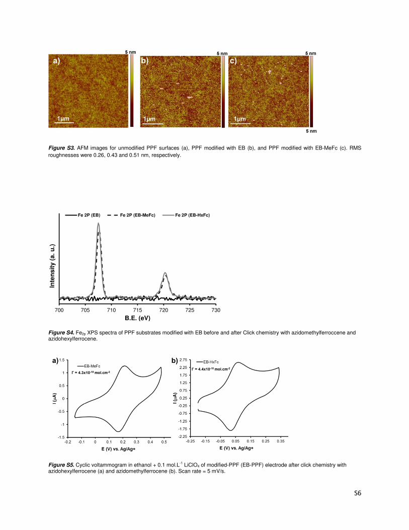
Figure S3. AFM images for unmodified PPF surfaces (a), PPF modified with EB (b), and PPF modified with EB-MeFc (c). RMS
roughnesses were 0.26, 0.43 and 0.51 nm, respectively.
Figure S4. Fe2p XPS spectra of PPF substrates modified with EB before and after Click chemistry with azidomethylferroccene and azidohexylferrocene.
Figure S5. Cyclic voltammogram in ethanol + 0.1 mol.L-1 LiClO4 of modified-PPF (EB-PPF) electrode after click chemistry with
azidohexylferrocene (a) and azidomethylferrocene (b). Scan rate = 5 mV/s.
700 705 710 715 720 725 730
Inte
nsit
y (
a. u
.)
B.E. (eV)
Fe 2P (EB) Fe 2P (EB-MeFc) Fe 2P (EB-HxFc)

S7
Table S1. Yield and reproducibility of EB-based junctions with and without coupling to different azides by click chemistry. Ra is the
root mean square (RMS) roughness from AFM for the indicated surfaces before top contact deposition. The relative standard
deviations calculated for the junctions illustrated in Figure1 and Figure 2 of the main text. The overall yield for the fabricated devices
is 92% and 100% for the ferrocene and alkane series, respectively.
Figure S6. Overlay of 15 Junctions from two samples composed of PPF/ EB coupled to hexylferrocene by click chemistry followed
by top contact deposition.
-11
-9
-7
-5
-3
-1
1
-1 -0.75 -0.5 -0.25 0 0.25 0.5 0.75 1
ln J
(A c
m-2
)
V (V)
Overlay of 15 junctions from two samples
Samples # of junctions
Ra, nm
Yield RSD0.1 V
EB (2.2 ± 0.5 nm) 16 0.426 14/16 25.8 %
EB-MePh(3.3 ± 0.4 nm) 16 0.513 14/16 10.2%
EB-MeFc (3.4 ± 0.6 nm) 16 0.437 16/16 21.3 %
EB-HxFc(3.9 ± 0.7 nm) 16 0.508 15/16 6.70 %
Alkane Series
EB (2.6 ± 0.5 nm ) 8 0.68 8/8 13.6 %
EB-C8 (3.00 ± 0.6 nm) 8 0.49 8/8 1.18 %
EB-C12 (3.30 ± 0.6 nm) 8 0.44 8/8 4.80 %
EB-C16 (3.78 ± 0.5 nm) 8 0.46 8/8 6.40%

S8
Figure S7. Overlay of J-V curves for a EB-MePh junction after eight months exposure to ambient air.
Figure S8. (a-c) J-V curves for PPF/molecule/e-C/Au junctions containing ferrocene and methyl-phenyl layers, as indicated, in the
temperature range from 100-400 K. (d-f) Arrhenius plots at different bias voltages.
-4.5
-2.5
-0.5
1.5
3.5
5.5
-0.8 -0.4 0 0.4 0.8
J(A
cm
-2)
V (V)
EB-MePh
EB-MePh after eight months
-5
-3
-1
1
3
5
7
-0.75 -0.5 -0.25 0 0.25 0.5 0.75
J(A
cm
-2)
V (V)
EB-MePh, 100 K
EB-MePh, 210 K
EB-MePh, 300 K
EB-MePh, 400 K
-4
-3
-2
-1
0
1
2
2 4 6 8 10
ln J
1000/T (K-1)
0.15V
0.3V
0.5V
-6
-5
-4
-3
-2
-1
0
1
2 4 6 8 10
ln J
1000/T (K-1)
0.15V
0.3V
0.5V
d) e)
EB-MeFc EB-HxFc-3
-2.5
-2
-1.5
-1
-0.5
0
0.5
1
1.5
2 4 6 8 10
ln J
1000/T (K-1)
0.2V0.3V0.5V
EB-MePh
f)
-5.5
-3
-0.5
2
4.5
-0.8 -0.4 0 0.4 0.8
J (
A/c
m-2
)
V(V)
EB-MeFc, 100 K
EB-MeFc, 210 K
EB-MeFc, 300 K
EB-MeFc, 400 K
-5
-2.5
0
2.5
5
-1 -0.5 0 0.5 1
J (
A/c
m-2
)
V (V)
EB-HxFc, 100 K
EB-HxFc, 210 K
EB-HxFc, 300 K
EB-HxFc, 400 K
a) b) c)

S9
Figure S9. (a-c) A series of J-V curves in the temperature range from 100-400 K. (d-f) Arrhenius plots at different biases.
100 – 210 K 300 – 400 K
0.2 V 0.5 V 0.2 V 0.5 V
EB-MeFc 3.70 1.60 56.2 54.4
EB-HxFc 7.93 4.80 114 94.8
EB-MePh 4.21 3.43 44.0 35.2
EB-C8 3.90 1.20 47.0 36.3
EB-C12 6.50 4.20 68.2 53.1
EB-C16 1.60 0.80 46.2 32.4
Table S2. Arrhenius slopes for various junctions of EB modified by click chemistry with MeFc, MePh, HxFc, C8, C12, and C16.
-4
-3
-2
-1
0
1
2 4 6 8 10
ln J
1000/T (K-1)
0.2V 0.3V
0.4V 0.5V
-4.5
-3.5
-2.5
-1.5
-0.5
0.5
2 4 6 8 10
ln J
1000/T (K-1)
0.2V 0.3V
0.4V 0.5V
e) f)EB-C12 EB-C16
-2.5
-2
-1.5
-1
-0.5
0
0.5
1
1.5
2
2.5
2 3 4 5 6 7 8 9 10
ln J
1000/T (K-1)
0.2V 0.3V
0.4V 0.5V
d) EB-C8
-6
-4
-2
0
2
4
6
-0.75 -0.375 0 0.375 0.75
J(A
cm
-2)
V (V)
EB-C8, 100k
EB-C8, 200k
EB-C8, 300k
EB-C8, 400k
-8
-4
0
4
8
12
-0.9 -0.45 0 0.45 0.9
J(A
cm
-2)
V (V)
EB-C12, 100 K
EB-C12, 200 K
EB-C12, 300 K
EB-C12, 400 K
-5
-3
-1
1
3
5
7
-1.2 -0.6 0 0.6 1.2
J(A
cm
-2)
V (V)
EB-C16, 100 KEB-C16, 200 KEB-C16, 300 KEB-C16, 400 K
b) c)a)

S10
Figure S10. J-V curves for different t EB-based junctions fit to the Simmons model as described previously
13. The black dots are the
experimental data, while the gray broken lines are the results of the full Simmons model, where the parameters obtained are indicated.
Measurement of Molecular Layer Thickness
Molecular layer thicknesses were determined with AFM “scratching” as described previously 14, with a more detailed statistical
analysis described below. In contact mode, an area of 1µm x 1µm was scanned under a set point of (0.25 V). As a result the
molecular film was removed without scratching the PPF leaving a trench, which is used to determine the height of the molecular
layer after scanning a larger area (5µm x 5µm) of the same spot in tapping mode (figure S11). The molecular layer thickness was
determined as the difference in heights between the bottom of the trench and the top of the surrounding molecular layer. Two
histograms, for the heights of the trench and the surrounding area were fit by two different Gaussian functions (figure 12).
Thicknesses stated in main text are the difference of the centers of the Gaussian distribution, with the uncertainty in thickness
stated as the quadrature addition of the two best-fit σ values.
-10
-8
-6
-4
-2
0
2
4
-1.2 -0.9 -0.6 -0.3 0 0.3 0.6 0.9 1.2
-8
-6
-4
-2
0
2
4
-1 -0.75 -0.5 -0.25 0 0.25 0.5 0.75 1
ln J
(A
cm
-2)
V (V)
-9
-6
-3
0
3
-0.75 -0.5 -0.25 0 0.25 0.5 0.75V (V)
-8
-6
-4
-2
0
2
4
-0.3 -0.2 -0.1 0 0.1 0.2 0.3
lnJ
(A
cm
-2)
V (V)
PPF/EB PPF/EB/C8
εεεε 4.14
me 0.8
φφφφ 1.22 eV
d 3.00 nm
εεεε 2.5
me 1.53
φφφφ 1.3 eV
d 2.57 nm
εεεε 5.6
me 0.80
φφφφ 1.12 eV
d 3.30 nm
εεεε 9.01
me 0.40
φφφφ 1.32 eV
d 3.80 nm
PPF/EB/C12
PPF/EB/C16
lnJ (
A c
m-2
)ln
J (
A c
m-2
)
V (V)
(a)
(c)
(b)
(d)

S11
Figure S11. AFM images of trenches made in molecular layers of EB (a), EB-MeFc (b), EB-MePh (c), and EB-HxFc (d) on carbon
(PPF).
Figure S12. Fitting of the AFM height data generated as a histogram from the images shown in Figure S11, i.e. EB (a), EB-MeFc
(b), EB-MePh (c), and EB-HxFc (d)
0
0.2
0.4
0.6
0.8
1
1.2
1.4
4 6 8 10 12 14
% P
oin
ts
Height (nm)
AFM Histogram DataGaussian Fit x1Gaussian Fit x2
d = 2.23 nm
0
0.2
0.4
0.6
0.8
1
1.2
0 3 6 9 12
% P
oin
ts
Height (nm)
AFM Histogram DataGaussian Fit x1Gaussian Fit x2
d = 3.35 nm
0
0.5
1
1.5
2
2.5
3
3.5
18 20 22 24 26
% P
oin
ts
Height (nm)
AFM Histogram Data
Gaussian Fit x1
Gaussian Fit x2
d = 3.26 nm
0
0.2
0.4
0.6
0.8
1
1.2
1.4
0 5 10 15
% P
oin
ts
Height (nm)
AFM Histogram DataGaussian Fit x1Gaussian Fit x2
a) b)
c) d)
d = 3.93 nm

S12
Figure S13. AFM images of trenches made in molecular layers of EB (a), EB-C8 (b), EB-C12 (c), and EB-C16 (d) on carbon (PPF).
Figure S14. Fitting of the data generated as a histogram from the AFM data shown in Figure S13, i.e. EB (a), EB-C8 (b),
EB-C12 (c), and EB-C16 (d).
0
0.5
1
1.5
2
2.5
6 10 14 18
% P
oin
ts
Height (nm)
AFM Histogram Data
Gaussian Fit x1
Gaussian Fit x2
0
0.4
0.8
1.2
1.6
5 7 9 11 13 15
% P
oin
ts
Height (nm)
AFM Histogram Data
Gaussian Fit x1
Gaussian Fit x2
0
0.2
0.4
0.6
0.8
1
1.2
1.4
0 5 10 15
% P
oin
ts
Height (nm)
AFM Histogram Data
Gaussian Fit x1
Gaussian Fit x2
0
0.4
0.8
1.2
1.6
2
3 5 7 9 11 13
% P
oin
ts
Height (nm)
AFM Histogram Data
Gaussian Fit x1
Gaussian Fit x2
d = 2.57 nm
d = 3.30 nm
c) d)
a) b)
d = 3.0 nm
d = 3.78 nm

S13
Figure S15. (a) Overlay of UPS spectra for EB junctions before and after click reaction with azidoalkanes (a); the spectra are presented near the PPF Fermi level to determine the EHOMO,onset. (b) Plot of the calculated average barrier for junctions made out of EB (2.57 nm) and increasing thiknesses of coupled alkanes. The inset equations was used to calculate the average barrier, where aliph = 1.2 eV and arom = 2.0 eV.
15
Figure S16. Fe2p XPS spectra of methylferrocene (a), and hexylferrocene (b) coupled by click chemistry on EB (method 2) and
deprotected-TMS (method 1).
Figure S17. Statistical distribution of ln J at 0.1 V for fifteen EB-HxFc junctions. Ordinate is the number of junctions exhibiting
conductances at 0.1 V in a range of 0.1 ln units. Solid line is a Gaussian distribution for comparison.
a) b)
1.25
1.4
1.55
1.7
1.85
2
0 4 8 12 16 20
ave
rag
e b
arr
ier
dCn(nm)
Average barrier () =
-2-1.5-1-0.500.511.52
Inte
nsit
y (
a.u
.)
B.E.
PPF
EB
EB+c8
EB+C12
EB+C16
700 705 710 715 720 725 730
Inte
nsit
y (
a.
u.)
B.E. (eV)
Fe 2P (Deprotected-TMS/MeFc) Fe 2P (EB-MeFc)
700 705 710 715 720 725 730
Inte
nsit
y (
a.
u.)
B.E. (eV)
Fe 2P (Deprotected-TMS/HxFc) Fe 2P (EB-HxFc)a)b)
-3.0 -3.5 -4.0 -4.5 -5.00
2
4
6
Co
unt
lnJ0.1 V

S14
Table S3. Values of the EHOMO,onset estimated from UPS measurements, barrier height from fitting the data to Simmons’s model, and
the average barrier calculated from coupling the EB layer with C8, C12, and C16.
References
(1) Casas-Solvas, J. M.; Vargas-Berenguel, A.; Capitán-Vallvey, L. F.; Santoyo-González, F.; Organic
Letters 2004, 6, 3687-3690.
(2) Lee, Y.; Morales, G. M.; Yu, L.; Angewandte Chemie - International Edition 2005, 44, 4228-4231.
(3) Baek, S. Y.; Kim, Y. W.; Yoo, S. H.; Chung, K.; Kim, N. K.; Kim, J. S.; Industrial and Engineering
Chemistry Research 2012, 51, 9669-9678.
(4) Lamani, M.; Prabhu, K. R.; Angewandte Chemie - International Edition 2010, 49, 6622-6625.
(5) Evrard, D.; Lambert, F.; Policar, C.; Balland, V.; Limoges, B.; Chemistry - A European Journal 2008, 14,
9286-9291.
(6) Leroux, Y. R.; Hapiot, P.; Chemistry of Materials 2013, 25, 489-495.
(7) Leroux, Y. R.; Fei, H.; Noël, J.-M.; Roux, C.; Hapiot, P.; Journal of the American Chemical Society
2010, 132, 14039-14041.
(8) Ranganathan, S.; McCreery, R. L.; Analytical Chemistry 2001, 73, 893-900.
(9) Ranganathan, S.; Kuo, T.-C.; McCreery, R. L.; Analytical Chemistry 1999, 71, 3574-3580.
(10) Yan, H.; Bergren, A. J.; McCreery, R. L.; Journal of the American Chemical Society 2011, 133, 19168-
19177.
(11) Blackstock, J. J.; Rostami, A. A.; Nowak, A. M.; McCreery, R. L.; Freeman, M.; McDermott, M. T.;
Analytical Chemistry 2004, 76, 2544-2552.
(12) Ru, J.; Szeto, B.; Bonifas, A.; McCreery, R. L.; ACS Applied Materials and Interfaces 2010, 2, 3693-
3701.
(13) Bergren, A. J.; McCreery, R. L.; Stoyanov, S. R.; Gusarov, S.; Kovalenko, A.; Journal of Physical
Chemistry C 2010, 114, 15806-15815.
(14) Anariba, F.; DuVall, S. H.; McCreery, R. L.; Analytical Chemistry 2003, 75, 3837-3844.
(15) Sayed, S. Y.; Fereiro, J. A.; Yan, H.; McCreery, R. L.; Bergren, A. J.; Proceedings of the National
Academy of Sciences 2012, 109, 11498-11503.
Sample EHOMO, onset
(eV)
φSimmons
(eV)
φaverage
(eV)
PPF/EB 1.28 ±0.04 1.30 1.20
PPF/EB/C8 1.28 ±0.04 1.22 1.31
PPF/EB/C12 1.20 ±0.01 1.22 1.38
PPF/EB/C16 1.25 ±0.04 1.32 1.46