summit - impedance, equivalent circuit and capacitance of double barrier resonant...
TRANSCRIPT
IMPEDANCE, EQUIVALENT CIRCUIT AND CAPACITANCE OF
DOUBLE BARRIER RESONANT TUNNELING DIODE
by
Tao Wei
B.Sc. Peking University 1983
M.Sc. Peking University 1986
M.Sc. Simon Fraser University 1990
THESIS SUBMI'ITED IN PARTIAL FULFILLMENT OF
THE REQUIREMENTS FOR THE DEGREE OF
DOCTOR OF PHILOSOPHY
in the School
of Engineering Science
O Tao Wei 1994
SIMON FRASER UNIVERSITY
December 1994
All rights reserved. This work may not be
reproduced in whole or in part, by photocopy
or other means, without permission of the author.

APPROVAL
Name:
Degree:
Title of Thesis:
Tao Wei
Doctor of Philosophy
Impedance, Equivalent Circuit and Capacitance of Double Barrier Resonant Tunneling Diode
Examining Committee: Dr. G l e ~ Chapman Chair
Date Approved:
Dr. Shawn Stlfpltton Senior Supervisor
Dr. Jarnal Deen Supervisor
- Dr. Steve Hardy Supervisor
Dr. David Corn External Examiner McMaster University
Dr.*. Parameswarm Internal Examiner
2 December, 1994

PARTIAL COPYRIGHT LICENSE
I hereby grant to Simon Fraser University the right to lend my thesis, project or extended
essay (the title of which is shown below) to users of the Simon Fraser University Library, and
to make partial or single copies only for such users or in response to a request from the library
of any other university, or other educational institution, on its own behalf or for one of its
users. I further agree that permission for multiple copying of this work for scholarly purposes
may be granted by me or the Dean of Graduate Studies. It is understood that copying or
publication of this work for financial gain shall not be allowed without my written permission.
Title of Thesis/Project/Extended Essay
"Impedance. Eauivalent Circuit and Capacitance of Double Barrier Resonant
Tunnelin Diode"
Author: (signature)
December 2.1994 (date)

ABSTRACT
By employing scattering parameter (S parameter) measurements with on-wafer
probing techniques, we have measured accurate small signal impedances for two different
double barrier quantum well resonant tunneling diodes (RTDs) up to 40GHz. It was found
that the impedances can be very well described by an equivalent circuit that consists of a
parallel admittance-capacitance (G-C) and a series resistance-inductance (R-L) circuit. The
inductance was found to have resulted from the on-wafer connecting lines and the air-
bridge structure. The quantum well itself is represented by the parallel G-C circuit. With
the measured impedances and the equivalent circuit representation, capacitance-voltage
(C-V) and conductance-voltage (G-V) characteristics have been obtained.
Our experiment shows that the G-V characteristic obtained from the high
frequency measurement is comparable to that obtained from dc current-voltage (I-V)
characteristic. Using this comparison, the I-V characteristic that was distorted by self-
oscillations in the negative differential resistance (NDR) region of the dc measurement has
been recovered from the stable high frequency rf G-V characteristic. A hysteresis that is
not affected by oscillations was observed in the S parameter measurements. Our study
shows that this hysteresis is not due to the charge storage effect predicted by theory, but
to the load-line bistability of the internal series resistance.
We have proposed a new capacitance calculation scheme and calculated the
capacitances for RTDs, based on the charge distributions obtained from self-consistent
calculations. The calculated C-V characteristics agree qualitatively with experimental

results. Both the theoretical and experimental results show a capacitance peak in the NDR
region. Calculation indicates that the peak is caused by electrons discharging from the
quantum well, rather than from the charge accumulations in the quantum well as was
formerly believed. Also observed was an additional smaller capacitance peak
corresponding to electrons discharging from the accumulation region adjacent to the
emitter barrier.
We have theoretically studied the effects of the spacer layers on the capacitance.
Analysis indicates that the capacitance peak in the NDR region is very sensitive to
variations in the cathode spacer layer. The anode spacer layer has a relatively limited effect
on the peak. Increasing the anode spacer layer can decrease the capacitance in general and
increase the cutoff frequency of the RTD. The effects of the fixed interface space charge
on I-V and C-V characteristics have also been considered. The device performance is
found to be degraded slightly by the presence of a fixed space charge of normal density.

ACKNOWLEDGMENT
I wish to thank Dr. Stapleton, who supervised and encouraged this research. I
would also like to thank Dr. Y. Hu, Dr. 0. Berolo, S. Rambaran, S. Bernhoff, W. Coyne,
and P. Borkowski for their help and suggestions. My thanks also go to Dr. D. Conn, Dr. J.
Deen, Dr. S. Hardy, Dr. M. Pararneswaran and Dr. G. Chapman, who examined and
reviewed all chapters carefully.
I gratefully acknowledge the financial support provided by my supervisor S.
Stapleton and the University Fellowship by Simon Fraser University.

TABLE OF CONTENTS
. . ........................................................................................................................ Approval 11
... ........................................................................................................................ Abstract 111
........................................................................................................... Acknowledgment V
1 . Introduction ............................................................................................................... 1
.................................................................................................. 1.1 Background 1
1.2 Overview of Thesis Work ............................................................................. 6
1.3 Thesis Outline ............................................................................................. 10
2 . Experimental ............................................................................................................ 12
2.1 Device Structures. Layouts and Fabrications ............................................... 12
2.2 I-V and S Parameter Measurements ............................................................ 17
3 . Theoretical Calculations ........................................................................................... 23
3.1 The Schrodinger Equation Solution for an One-Dimensional
Quasi-Static RTD Model ....................................................................... 23
3.2 Solution of Poisson wuation ...................................................................... 30
3.3 Self-consistent Calculation ........................................................................ 32
3.4 Capacitance Calculation .............................................................................. 36
4 . Results and Discussions ........................................................................................... 42
4.1 Impedance. Equivalent Circuit and C-V Characteristic:

4 . G . Diode. up to 1 8GHz .............................................. 4 %6 42
.............................................. Equivalent Circuit and Impedance 44
.................. C-V Characteristic: Compared to Theoretical Result 52
Cutoff Frequency ....................................................................... 60
4.2 Impedance, Equivalent Circuit and C-V Characteristics:
4 . G As-GAs Diode, up to 4GHz ............................................... 4 %.6 62
4.3 Impedance, Equivalent Circuit and C-V Characteristic:
AIAs-GaAs Diode, up to 4 G H z ........................................................... 68
Hysteresis .................................................................................. 70
C-V Characteristic and Cutoff Frequency ................................... 76
4.4 Effects of Spacer Layers on C-V Characteristic: Theoretical
Considerations ...................................................................................... 80
4.5 Effects of Fixed Space Charge on I-V and C-V Characteristics:
LIST OF FIGURES
Fig.1.1.1 Schematic diagram of the tunneling mechanism in RTD ............................ 2
Fig.l.l.2 Equivalent circuit used for the resonant tunneling diode ........................... 4
Fig.2.1.1 Schematic cross sectional view of the &.4G~.6As.GaAs
RTD structure ............................................................................ 13
Fig.2.1.2 Schematic cross sectional view of the A1As-GaAs diode structure .......... 14
Fig.2.1.3a)-b) Layout and schematic cross sectional view of a fabricated RTD.--.- 15- 16
........................... Fig.2.2.1 Experimental setup for I -V characteristic mesurements 18
................................... Fig.2.2.2 Experimental setup for S parameter mesurements 20
........... Fig.3.1.1 Discretisation of a continuously varied conduction band potential 25
Fig.3.3.1 Calculated conduction band potential and electron density distribution . -35
....................................................... Fig.3.4.1 Calculated space charge distribution 37
.................................. Fig.3.4.2 Schematic vaiation of electron density distribution 39
........... Fig.4.1.1 Experimental I-V characteristic for the 4 4G~.6As43iAs diode 43
Fig.4.1.2a)-d) Measured and calculated impedance of RTD under some voltages . -45-48
.............................................. Fig.4.1.3 Measured &/m/ and calculated 1 / ( ~ d +R $1 50
...................... Fig.4.1.4 C-V characteristic obtained from impedance measurement 51
...... Fig.4.1.5 Experimental C-V and G-V curves for the 4 3 G ~ 7As-GaAs RTD .54
........... Fig.4.1.6 Calculated C-V and G-V curves for the &.3Ga0.7As.GaAs RTD 56
............................ Fig.4.1.7 Calculated electron distributions and potential profiles 57

Fig.4.2.1 I-V characteristic for another Al03Gag 7As-GaAs RTD. ......................... 63
Fig.4.2.2a)-b) Measured and calculated impedances of the diode. ........................... 64-65
Fig.4.2.3 C-V and G-V characteristics obtained from impedance measurements. -67
............................................. Fig.4.3.1. I -V characteristic of the AIAs-GaAs diode. 69
Fig.4.3.2a)-b) Measured and calculated impedances of the diode. ............................ 7 1-72
............................................... Fig.4.3.3 C-V and G-V characteristics of the diode. 7 3
................................. Fig.4.3.4 Schematic diagram of load-line bistability of RTD. 7 5
................... Fig.4.3.5 Calculated C-V and G-V characteristics under forward bias. 77
Fig.4.3.6 Calculated conduction band potential and electron density distribution. -78
Fig.4.4.la)-b) Calculated I -V characteristics for RTDs with various spacer layers. -82-83
................... Fig.4.4.2 Calculated C-V and G-V characteristics under forward bias. 84
Fig.4.4.3 Calculated C-V and G-V characteristics for diodes under reverse bias. -85
Fig.4.4.4 Conduction band diagram and electron density for the ~ O O A diode. ---87
Fig.4.5.1. Calculated I -V characteristics for RTDs with interface space charge. --90
Fig.4.5.2. Calculated C-V characteristics for RTDs with interface space charge. --91

CHAPTER 1. INTRODUCTION
1.1 Background
Progress in semiconductor heterostructure growth technology, particularly in the
epitaxial technology, has permitted the fabrication of nanometer structures whose behavior
is dominated by quantum interference effects. The quantum well resonant tunneling diode
(RTD) is the direct result of such technological progress. In 1973, Tsu and Esaki (Tsu and
Esaki, 1973) suggested that the tunneling mechanism of the supperlattice structure should
lead to a negative differential resistance (NDR) in the current-voltage (I-V) characteristic.
In 1974, the fist double barrier quantum well resonant tunneling diode was fabricated
(Chang et al., 1974) and NDR was observed at low temperatures.
The most important component of a RTD is the double barrier quantum well
structure (Fig.l.l.la). Usually the quantum well consists of a narrow bandgap material
and the barriers consist of wide bandgap materials (referred to as type I heterostructure).
A GaAs well and AlXGal_,As barriers represent one example of a type I heterostructure
quantum well. Ideally, when the kinetic energy of an electron Ex is in resonance with the
quasi-bound state Ew in the well, the transmission coefficient attains its maximum (for an
symmetric quantum well it becomes unity). As the diode is biased and E, is lowered to the
Fermi level, current through the device increases. When Ew and the bottom of the emitter
conduction band are aligned, current through the device is at a maximum (Fig.l.1. lb).
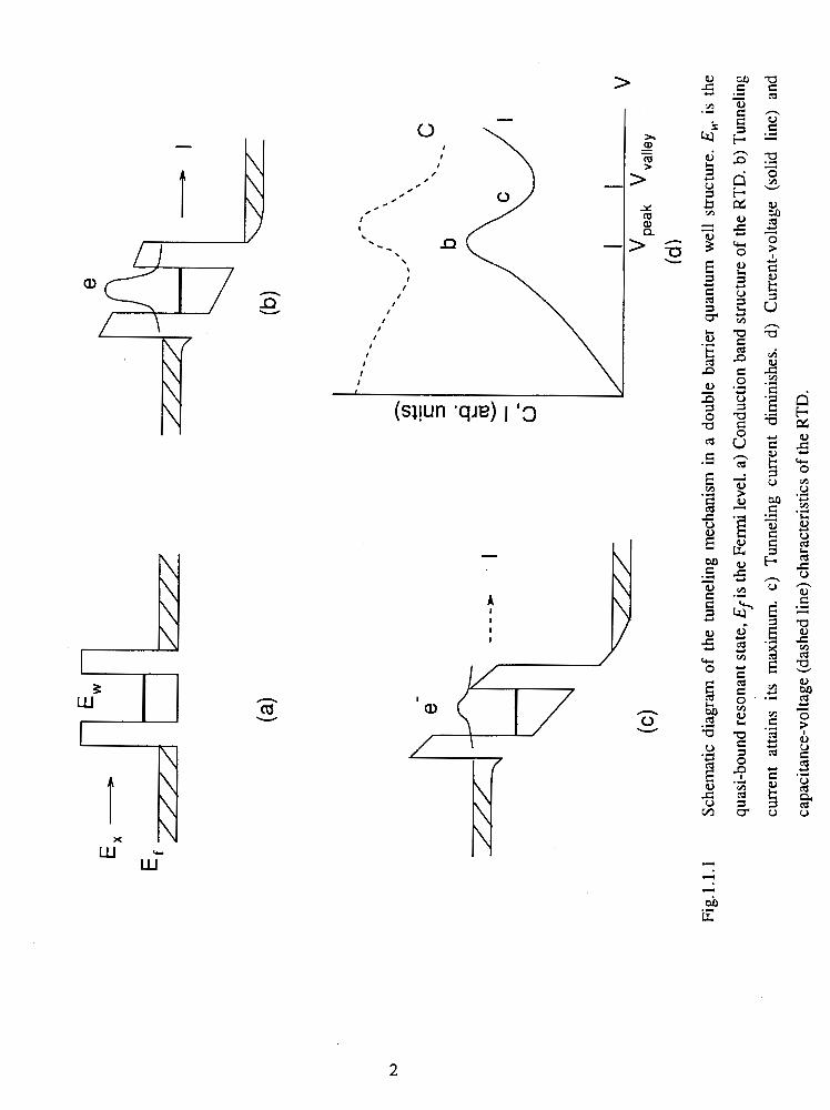
Fi
ll
1
Sche
mat
ic d
iagr
am o
f th
e tu
nnel
ing
mec
hani
sm i
n a
doub
le b
arri
er q
uant
um w
ell
stru
ctur
e. E
,. is
the
quas
i-bo
und
reso
nant
sta
te, Ef
is th
e Fe
rmi l
evel
. a)
Con
duct
ion
band
str
uctu
re o
f th
e R
TD
. b)
Tun
nelin
g
curr
ent
atta
ins
its
max
imum
. c)
Tun
nelin
g cu
rren
t di
min
ishe
s.
d) C
urre
nt-v
olta
ge
(sol
id
line)
and
capa
cita
nce-
volt
age
(das
hed
line
) cha
ract
eris
tics
of
the RTD.

Biasing the diode beyond this point causes the current to decrease, giving rise to a NDR
(Fig.l.l.1~). Associated with the change in the current is a change in electron density
distribution. As indicated in Fig. 1.1.1, both electron density in the well and current
approach their maximum levels simultaneously at the peak voltage Vpeak Both decrease
when the RTD is biased into the NDR region and reach their minimum levels at the valley
voltage Vvalley
Due to the simplicity of its structure, the RTD is ideally suited for basic research
on physics phenomena of nanostructure quantum systems, especially with respect to the
transport properties,. Early RTD studies focused primarily on fundamental physics. In
1983, Sollner et al. (Sollner et al., 1983) demonstrated the detection capabilities of RTDs
up to 2.5THz. Their findings quickly stimulated further study on the application aspects of
the diode (for examples, see Capasso et al., 1986; articles in Sze, 1990 and Capasso,
1990). To date, many high speed analog and digital applications have been found for the
device. Examples of these applications are high frequency oscillators (Sollner et al., 1987;
Brown et al., 1987 and 1989), mixers (Mortazawi et al., 1989; MiUington et al., 1991,
Krishnamurthi and Conn, 199 I), multipliers (Batelaan and Frerking, 1987; Sollner et al.,
1988; Sen et al., 1988), high speed analog-to-digital converters (Capasso, 1990) and
multi-state memory devices (Capasso et al., 1986; Raychaudhuri and Deen, 1993).
For circuit design purposes, especially for ac and rf applications, an equivalent
circuit representation is essential. For testing an equivalent circuit under experimental
conditions, impedance measurement is the most direct technique. Since the invention of

the diode, a number of equivalent circuits have been proposed and tested (Gering et al.,
1987; Sheard and Toombs, 1987; Kesan et al., 1988 and 1989; Lippens and Mounaix,
1988; Brown et al., 1989; Zarea et al., 1990; Genoe et al., 1991; Miles et al., 1991;
Schernrnann et al., 1991; Whitson et al., 1991; Vanbesien et al., 1992). Except for a few
cases (Sheard and Toombs, 1987; Miles et al., 1991; Genoe et al., 1991), most of these
models featured the equivalent circuit used for the Esaki diode. The later consists a
parallel (lumped) resistance-capacitance circuit, a series resistance and a series inductance
(Fig. 1.1.2). In some cases, only the Esaki diode equivalent circuit was employed (Gering
et al., 1987; Lippens and Mounaix, 1988; Zarea et al., 1990; Schemmann et al., 1991).
Fig.l.l.2 Equivalent circuit used for the resonant tunneling diode. Parallel R-C
circuit represents the quantum well structure. The series R-L circuit
accounts for the remaining structures.
However, all of these circuits were tested either over a limited frequency range or under
very restricted bias conditions. The main reason for these approaches was that spurious
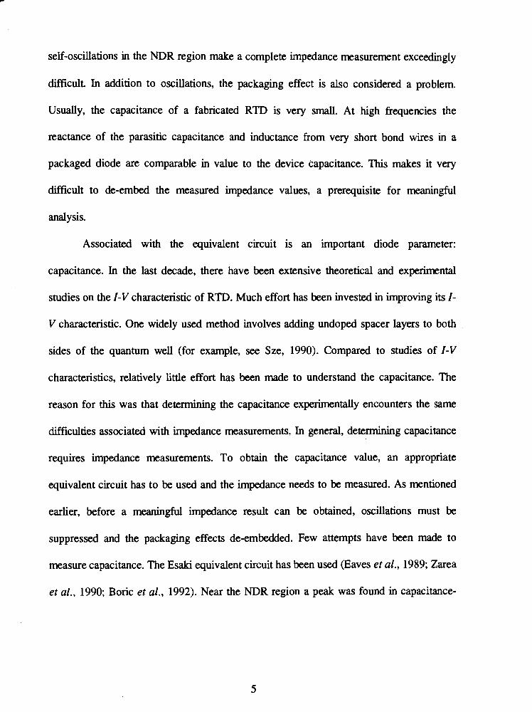
self-oscillations in the NDR region make a complete impedance measurement exceedingly
difficult. In addition to oscillations, the packaging effect is also considered a problem.
Usually, the capacitance of a fabricated RTD is very small. At high frequencies the
reactance of the parasitic capacitance and inductance from very short bond wires in a
packaged diode are comparable in value to the device capacitance. This makes it very
difficult to de-embed the measured impedance values, a prerequisite for meaningful
analysis.
Associated with the equivalent circuit is an important diode parameter:
capacitance. In the last decade, there have been extensive theoretical and experimental
studies on the I -V characteristic of RTD. Much effort has been invested in improving its I-
V characteristic. One widely used method involves adding undoped spacer layers to both
sides of the quantum well (for example, see Sze, 1990). Compared to studies of I-V
characteristics, relatively little effort has been made to understand the capacitance. The
reason for this was that determining the capacitance experimentally encounters the same
difficulties associated with impedance measurements. In general, determining capacitance
requires impedance measurements. To obtain the capacitance value, an appropriate
equivalent circuit has to be used and the impedance needs to be measured. As mentioned
earlier, before a meaningful impedance result can be obtained, oscillations must be
suppressed and the packaging effects de-embedded. Few attempts have been made to
measure capacitance. The Esaki equivalent circuit has been used (Eaves et al., 1989; Zarea
et al., 1990; Boric et al., 1992). Near the NDR region a peak was found in capacitance-

/
voltage (C-V) characteristics. Schubert et al. (1990) attributed the peak to the charge
accumulation in the quantum well. According to their interpretation the capacitance peak
should coincide with the current peaks in the I-V characteristics. However, most of the
measurements failed to provide accurate results. Moreover, Boric et al. (1992) pointed
out that the peak might in fact shift toward higher voltages in the NDR region. Employing
theoretically physical models, some researchers have calculated the capacitance of
quantum well structures; however, no peak feature was found (Yokoyama, 1989; Sun et
al., 1992). Understanding of the capacitance behavior of the RTD will require more
careful measurement and more comprehensive theoretical studies.
1.2 Overview of Thesis Work
Our experimental work involved measuring the microwave frequency small signal
scattering parameters (S parameters) of RTDs. Diode impedances were obtained from the
S parameters. To eliminate packaging effects, we have used the on-wafer probing
technique. Two different quantum well structures were studied. One of them consists of
the &4G~.6As-GaAs barrier-well structure, the other consists of the AlAs-GaAs
structure. We first measured S parameters for & 4G~.6As-GaAs diodes up to 18GHz at
SFU (Wei, Stapleton and Berolo, 1993), and later extended the frequency range to 40GHz
at the Communications Research Centre (CRC) in Ottawa (Wei, Stapleton and Berolo,
1995a). We also measured AlAs-GaAs diodes up to 40GHz at CRC (Wei, Stapleton and
Berolo, 1995b). We found that, part of the oscillation power can couple into the network

analyzer and distort the S parameter signal. However, in most cases, oscillation
frequencies were below 2GHz. It was also discovered that, if the high frequency
components were not very strong, the oscillations would affect low frequency signals only.
Thus, analysis could be carried out on reliable high frequency data. It was further
discovered that, except for distorted low frequency signals, impedances obtained over the
whole frequency range and under various biases could be reproduced quite successfully by
the Esaki equivalent circuit (shown in Fig. 1.1.2). In the equivalent circuit the parallel
admittance-capacitance (G-C) structure represents the active quantum well region of the
RTD, the series resistance R, is associated with the contact and spreading resistance in the
semiconductor and the inductance L, is related to the connecting wires. With the
equivalent circuit, capacitance C, conductance (admittance) G and series resistance R,
were extracted from the measured impedance (hereafter G and dynamic resistance Rd=l/G
will be used interchangeably). It was found that the G-V characteristic is-directly
comparable to the derivative of the dc I-V characteristic. Peaks were observed in C-V
characteristics for all diodes. These peaks were found not in the peak voltages as formerly
predicted, but, rather, in the NDR regions. With respect to ALAS-GaAs diodes, a smaller
capacitance peak at a lower voltage was also observed.
Oscillations in the NDR region are usually very difficult to suppress. They have
been known to distort dc and low frequency ac measurements. Simulations have shown
that the oscillations can distort the dc I-V measurements and produce some jumps and
hysteresis in the NDR regions (Soher, 1987; Liu, 1988; Belhadj et al., 1990). These

jumps and hysteresis were found in some of our I-V measurements. Our S parameter
measurements indicated that, however, if the oscillations are weak and the frequencies are
not very high, the impedance obtained at higher frequencies will be affected very little and
a smoothly varied G-V characteristic can be extracted. Based on the fact that conductance
G is directly related to the derivative of I-V curve, we were able to recover an undistorted
I-V curve by integrating the G-V characteristic.
A hysteresis in the NDR region was observed in the S parameter measurement as
well as the dc I-V measurements for AlAs-GaAs diodes. The hysteresis phenomenon was
originally observed in dc I-V measurements and attributed to the charge storage effect
(Goldrnan et al., 1987; Kluksdahl et al., 1989). However, studies indicate that the
hysteresis may result from oscillations in the NDR regions (Sollner, 1987; Liu, 1988;
Belhadj et al., 1990). Simulations have shown that oscillations will distort the dc I-V
characteristic and produce a hysteresis effect very similar to that observed in the dc I-V
measurements (Liu, 1988; Belhadj et al., 1990). In this study it will be demonstrated that
(i) the hysteresis observed in the S parameter measurements is intrinsic and not affected by
oscillations; (ii) the hysteresis does not necessarily result from charge storage effects, but
from load-line effects caused by a relatively large series resistance (Okean, 1971; Jogai,
and Koenig, 1991; Chen et al., 1991).
To simulate C-V characteristics, we have calculated the capacitances of RTDs, on
the basis of electron density distributions obtained from quasi-static self-consistent
calculations (Stapleton and Wei, 1994; Wei and Stapleton, 1995~). The self-consistent

calculations were performed by iteratively solving the time-independent Schrodinger
equation and the Poisson equation. Theoretical C-V characteristics agree qualitatively with
experimental results. Our results show that the peak in the C-V c w e is attributable to the
quantum well discharging process, which occurs in the NDR region, rather than the charge
accumulation in the well as was formerly believed (Schubert et al., 1990). Calculation also
shows that the additional peak observed in the MAS-GaAs diodes results from electrons
discharging from the accumulation region between the emitter barrier and cathode spacer
layer.
The calculated capacitance peaks were found to be higher than experimental ones,
owing to scattering effects. The later, while considered important with respect to transport
mechanism (Kluksdahl et al., 1989; Frensley, 1990; Hu and Stapleton, 1991) were
excluded from our treatment in order to simplify calculations. Notwithstanding this
limitation, the results still provide a useful guideline for optimizing the diode structure for
high speed applications. We have calculated the capacitance of four A ~ O ~ G ~ ~ . J A S - G ~ A S
RTDs with identical quantum well structure but different spacer layers (Wei and
Stapleton, 1994). The results show that, capacitance generally decreases with an
increasing spacer layer. When the cathode spacer layer is increased, the capacitance peak
in the NDR region increases very rapidly and then decreases; when the anode spacer layer
is increased, the peak only broadens and decreases slightly. Compared to the change (of
the peak) resulting from variation in the cathode spacer layer, the effect of varying the
anode spacer layer on the peak is relatively small. When we compare the cutoff

frequencies of RTDs with different spacer layers, it is found that the high frequency
performance of a RTD can be improved by increasing the anode spacer layer.
By including the fixed space charge in the self-consistent calculation, we were able
to take into account the effect of the fixed interface space charge on the I-V and C-V
characteristics (Wei and Stapleton, 19954). It was found that the fixed space charge does
not significantly affect the current peak to valley ratio; but it does increase the capacitance,
and thereby, degrades the high frequency performance of the device. However, for a
typical fixed space charge density resulting fiom normal interface disorders, this
degradation was not found to be significant.
1.3 Thesis Outline
The experimental design and methodology are described in Chapter 2. The
theoretical model is delineated in Chapter 3.
Chapter 4 includes S parameter measurement results for two A.l~.~Gao&k-GaAs
RTDs, that range fiom 0 to 18GHz and 40GHz, respectively (4.1 and 4.2). These two
diodes feature identical quantum well structures, but due to the non-uniformity of the
wafer, their I-V characteristics are slightly different. We show that both devices produce
similar C-V and G-V results. However, with respect to oscillations in the NDR region, the
RTDs fall into two different categories. The RTD discussed in 4.1 had a relatively low
peak to valley ratio, the oscillations observed in the NDR regions were also very weak; in
the NDR regions the I-V characteristic was very smooth and remained virtually unaffected

by oscillations. The RTD discussed in 4.2 had a higher peak to valley ratio and stronger
oscillations in the NDR regions; in the NDR regions, the measured I-V characteristic was
distorted and some irregular jumps were observed. The first RTD is used to demonstrate
that the dc G-V characteristic is comparable to that obtained from rf measurements. The
second RTD is used to demonstrate that this comparableness makes it possible to restore
the distorted I-V characteristic from the almost oscillation-free rf results. In these two
sections we also compare the measured C-V results with the calculated results. In section
4.3, the experimental results for an AlAs-GaAs diode are presented and compared to the
theoretical results. Section 4.4 includes theoretical C-V characteristics for four
4 3G% 7As-GaAs diodes featuring different spacer layers. By comparing these results it
is possible to study the effect of different spacer layers on capacitance. We incorporated
the fixed interface space charge into the self-consistent calculation and calculated the I-V
and C-V characteristics. In section 4.5 the results are compared to that obtained without
the fixed space charge and the effects of the space charge on I-V and C-V characteristics
are estimated.
The conclusions are presented in Chapter 5.

CHAPTER 2. EXPERIMENTAL
2.1 Device Structures, Layouts and Fabrications
We have studied two different types of diodes, one consisting of an & 4 G ~ . 6 A ~ -
GaAs quantum well structure, the other of an AlAs-GaAs structure. The double barrier
quantum well wafers were grown at Bell-Northern Research Inc. in Ottawa, Ontario and
fabricated at the Communications Research Centre (CRC), also in Ottawa.
All double barrier quantum well structures were grown on semi-insulating GaAs
substrates employing molecular beam epitaxy (MBE). The & 4G~.6As-GaAs structure
was grown in the following series (Fig.2.1.1): i) 500A undoped GaAs, ii) WOOA n+-GaAs
contact layer (ND=5x10¹⁸ cmg, iii) 300A undoped GaAs spacer layer, iv) 4OA undoped
& . 4 G ~ b A ~ barrier, v) 50A undoped GaAs quantum well, vi) 4OA undoped
&.4Gw.6A~ barrier, vii) l00A undoped GaAs spacer layer, and viii) ~OOOA n+-GaAs
contact layer (ND=5x 1018 cm-3). The AlAs-GaAs structure was grown in a similar manner
as described in Fig.2.1.2. Note that both devices consist of symmetric quantum well
structures but feature asymmetric undoped spacer layers. Four identical &.4G~.6As-
GaAs wafers and two identical AlAs-GaAs wafers were processed and examined.
A typical RTD layout is illustrated in Fig.2.1.3(a). The schematic cross section
view of a fabricated diode is displayed in Fig.2.1.3(b). In the device fabrication, wet
chemical etching was used to isolate devices (dashed line in Fig.2.1.3(a) and slope area in

vi i i)
vii)
vi)
'4
iv)
iii)
i i)
i)
GaAs 5x1 d 8crn -3
GaAs undoped
AlGaAs undoped
GaAs undoped
AlGaAs undoped
GaAs undoped
GaAs 5x1 d 8cm
GaAs undoped
Semi-insulating GaAs
Fig.2.1.1 Schematic cross sectional view of the A ~ O . ~ G ~ ~ . ~ A S - G ~ A S double barrier
resonant tunneling diode structure. Diode structure was grown by MBE, on
a semi-insulating GaAs wafer.

viii)
vi i)
vi)
v)
iv)
iii)
i i)
GaAs undoped
AlAs undoped
GaAs undoped
AlAs undoped
GaAs undoped
GaAs 1 X I d8crn
GaAs undoped
Semi-insulating GaAs
Fig.2.1.2 Schematic cross section view for the AlAs-GaAs diode structure.


Fig.2.1.3(b)). Reactive ion etching (RE) was used to define diode areas (the smallest
square in Fig.2.1.3(a)) and to expose the underlying contact layer ii). With RIE, the active
region of a diode is vertically etched and the diode area is as laid-out (Fig.2.1.3(b)).
Diodes with areas ranging from 5x5 pm2 to 46x80 pm2 were fabricated. After etching,
the wafer was covered by a layer of Si3N4 to passivate the active diode region. Standard
Au/Ge/Ni ohmic contacts were fabricated on the contact layers viii) and ii). Each diode
was connected to a standard on-wafer microprobe ground-signal-ground pad
configuration. The signal pad was connected to layer viii) via a 50pm long low parasitic
capacitance air-bridge, the ground pads were connected to the first level metal contact
layer ii) (Fig.2.1.3(b)). To study the rf effects of the contact geometries alone, devices of
identical geometries but without active layers present were also fabricated (that is, contact
was made directly to the bottom contact layer ii)). In the following sections we shall refer
to them as short-circuited reference devices.
2.2 I-V and S Parameter Measurements
Some of the wafers under study were probed with standard Cascade micro-probes
(less than 26GHz) on a Cascade probing station at SF'U; others with Picoprober probes
(less than 60GHz) on a CKlOOO probing station at CRC. The probing stations were
mounted on air tables to be free of shocks and vibrations. The dc I -V characteristics were
measured with either a HP4145B semiconductor parameter analyzer or a HP4142B
modular dc source/monitor (Fig.2.2.1). To monitor oscillations in the NDR regions, an
oscilloscope or a spectrum analyzer was connected across the diode (Fig.2.2.1). It was


found that if the oscillations were weak, as for some small area &&ag6As-GaAs
diodes, smooth I -V characteristics were obtained. On the other hand, when the oscillations
were strong and could not be suppressed, the I-V characteristics showed some small jumps
and hysteresis, as predicted by simulations.
The S parameter data was collected by a HP851OB (up to 18GHz at SFU) and
HP8510C (up to 40GHz at CRC) network analyzers. To measure S parameters at various
voltages, we biased the diode by a low internal resistance dc power source, through the
built-in bias line (Fig.2.2.2). The total load line resistance was measured to be 1.5Q. In
some cases a bias tee connected to the probes was used and the load line resistance was
reduced to 0.6Q (because of a short connecting line). For measurements up to 18GHz, the
signal power level of the network analyzer was set at -10dBm. The real power delivered
to the probes was, however, attenuated by the connecting cables and consequently was
smaller. The signal power at the probes measured -23dBm (corresponding to -45mV
peak-to-peak in magnitude) at OSGHz and -32dBm (-15mVpp) at 18GHz, with the signal
at intermediate frequencies decreasing monotonically with increasing frequency. As the S
parameters were obtained by measuring the ratio of the reflected electromagnetic wave to
the incident wave, the non-uniformity of output power did not affect the accuracy of the
measurements. For measurements up to 40GHz, the signal power level was set at -5dBm.
The impedance Z can be calculated from the S parameter through the following
equation (Roddy, 1986):

Com
pute
r Con
trol
S
yste
m
Net
wor
k A
naly
zer
DC
Pow
er
Sou
rce
(or
Spe
ctru
m
Ana
lyze
r)
I I I
Osc
illos
cope
n
I I
I I
: DC
Pow
er
; I I
I
I I
: Sou
rce
I O
scill
osco
pe
j I
Fig.
2.2.
2 Sc
hem
atic
exp
erim
enta
l set
up f
or S p
aram
eter
mea
sure
men
ts. T
he R
TD
is b
iase
d ei
ther
thr
ough
the
bui
lt-
in b
ias
line
or a
bia
s-te
e co
nnec
ted
to t
he p
robe
(da
shed
lin
es).
The
osc
illat
ions
are
stu
died
by
repl
acin
g
the
netw
ork
anal
yzer
by
a sp
ectr
um a
naly
zer o
r an
osci
llosc
ope
(we
assu
me
that
the
osc
illat
ion
cond
itio
ns
rem
ain
the
sam
e as
the
inpu
t im
peda
nce
rem
ains
50R).
where S1 1 is the measured one port S parameter and ZO the 50SZ characteristic impedance
of the transmission lines. Ohmic measurements of the short-circuited reference devices
indicated that the total resistance of the air-bridge and the probe contacts was less than 0.2
a. The inductance of the air-bridges was found to be between 50pH to 70pH when the
probes were positioned in the middle of the probe pads and between l0pH and 40pH
when positioned very close to the device under test. The pads were 100xl00pd in size
(Fig.2.1.3(a)). A slight shift (-10-20pm) in probe positions was found to result in a
10-20pH change in the measured inductance. Consequently, the probe positions rernained
stationary during the whole measurement procedure. All measurements were made at
room temperature.
It is known that oscillations in the NDR region can sigdicantly affect
measurement results (Sollner, 1987; Liu, 1988; Belhadj et al., 1990). As it was usually
very difficult to suppress the oscillations, we decided to study smaller diodes where the
magnitudes (powers) of the oscillations were smaller. Before the measurements, the
network analyzer was replaced by a spectrum analyzer (or an oscilloscope), the bias was
adjusted and oscillation magnitudes were measured (Fig.2.2.1). Since the input impedance
of the spectrum analyzer (or oscilloscope) was the same as that of the network analyzer
(50Q), we assumed that the oscillation conditions were identical to that during the S
parameter measurements. During the S parameter measurement an oscilloscope was

connected to the bias circuit and used as an oscillation indicator (Fig.2.2.2). Since only
very low frequency (near dc) signals could couple into the dc bias circuit and the signal
observed on the oscilloscope was different from the signal that entered the network
analyzer, it was used only as a complementary oscillation indicator. Generally, the
variations of the oscillation magnitudes observed on the oscilloscope agreed with what we
had predicted from the oscillation measurements (before the S parameter measurements).
This observation supported our assumption that the oscillation signals observed before the
S parameter measurements were the same as those present during the S parameter
measurements. Our oscillation measurements showed that usually the oscillation
frequencies were relatively low (<2GHz). In the NDR region, especially in the middle
NDR area, the measured S parameters exhibited some irregular patterns at low frequencies
due to the oscillations (not smoothly varied in respect to the frequency, see Fig.4.1.2b, for
example). However the higher frequency signal was clean and smooth. When smooth
lower frequency data was not available, measurements were extrapolated from the more
reliable results obtained at high frequencies. We have examined almost all of the small
diodes on all wafers. On each wafer at least 4 diodes were carefully studied. For brevity,
only results obtained from some representative diodes are discussed in the following.

CHAPTER 3. THEORETICAL CALCULATIONS
3.1 The Schrodinger Equation Solution for an One-Dimensional Quasi-Static RTD
Model
A RTD under applied voltage is a complex non-equilibrium many-body system.
For theoretical purposes, we shall treat it by making some approximations. In particular,
we start by considering the RTD as an one-dimensional system We adopt the Hartree
approximation that assumes each electron moves in an average potential produced by all
other electrons (Thomas-Fermi screening potential), neglecting many-body interactions.
We use the effective-mass approximation to smooth out the microscopic structure of the
semiconductor. We assume that the system is stationary (equilibrium) under bias. To
reduce the amount of calculations involved, we also ignore all scattering effects. Previous
studies have shown that, without scattering effects, qualitatively correct I-V characteristic
can still be obtained, although the obtained valley current can be significantly large than
the reality (Cahay et al., 1986). So, with all these approximations, we expect that our
calculation would not provide us a quantitatively accurate result, but a qualitatively
correct picture. We can used this calculation to analyze our experimental results, to study
the tunneling mechanism, and to optimize the device structure for high speed applications.
The time-independent envelope function ~ ( x ) for an electron of energy E is
assumed to be given by the Schrodinger equation (Stem and Sarma, 1984):

where h is the Planck constant and m*(x) the position-dependent effective mass. V(x) is
the effective potential in which the electron moves:
V(x)=-e$(x)+Vh(x) (3.1.2)
variable e is the electron charge, $(x) the electrostatic potential, and Vh(x) the effective
potential associated with the heterojunction discontinuity. Note that the local exchange-
correlation energy has been neglected.
For the purpose of numerical calculation, we discretise a continuously varied
potential into a multi-step function of N segments (Fig.3.1.1). In each segment the
potential and effective mass are regarded as constants:
V,=V(x,) (3.1.3a)
and m,*=m*(x,), xj<x<xj+ 1 (3.1.3b)
Variables xg and x~ are located at the far ends of the device. Since the potential varies
greatly in the device, we used unequal segment widths, that is, smaller segment widths
were used when V changes rapidly with the coordinate x.
Given this approximation, the wavefunction between xj and x,, 1 can be written as:
ikj(x-x,) v j (x) = Aje + B je-ikj (x-x,)
where k = ,/2m * (E -Vj ) I h2 is the longitudinal wave vector (kinetic momentum); A,
and Bj are complex constants, they represent the forward and backward waves,
respectively .


The continuities of ~ ( x ) and yt(x)/m* (BenDaniel and Duke, 1966) at X=X,+~
require that:
and
The solutions for Eqs.(3.1.5) and (3.1.6) are:
where Dj is the transfer matrix:
Eq.(3.1.7) shows that (Aj, Bj) and (Ak, Bk) are closely related. To obtain all
Ajs and Bjs, and a complete solution of ~ ( x ) , the boundary conditions at both ends of the
device have to be considered.
Consider an electron of energy E and magnitude of unity injected from the far left
hand side of the device (Fig.3.l.l). At the far left hand side the wavefunctions of the
electron is described as below:
yo (X). = eiko (x-xo ) + R e-iko ) (3.1.9)
where R is the reflection coefficient. Since there is not reflection wave at the far right hand
side, at the far right hand side we have

where T is the transmission coefficient.
Now we define a new matrix
Applying Eq.(3.
and
1.7) sequentially to A,'s and B,'s gives rise to
From Eq.(3.1.12) we have the transmission and reflection coefficients
Knowing T and R, all A,'s and B,'s can be obtained from the following formulas
ajdj,l IT (3.1.15)
With A, and Bj the wavefunction, including magnitude and phase at all
coordinates, for an electron traveling from left to right is fully determined by Eq.(3.1.4).
Especially, at X=X> ~ ( x ) assumes the more simple form of
I~(X,)=A,+B~ (3.1.17)
The wavefunction from right to left may be calculated in a similar manner.

Knowing the transmission coefficient and thus the tunneling probability In2, it is
possible to calculate the current in the RTD. Here, we use Landauer's model (Landauer,
1970; Biittiker, 1986) in which the emitter and collector are assumed to be electron
reservoirs, that is, they can provide unlimited electrons and remain undisturbed by changes
in the device. Given these assumptions, the current from left to right can be obtained by
integrating the charge density times the tunneling probability:
where l ~ ~ ~ ( k ) l ~ is the tunneling probability fiom left to right and e the electron charge. f(k)
is the one-dimensional Ferrni-Dirac distribution function (Cahay et al., 1986; Hu, 1991):
kg is the Boltzmann constant, O the temperature and EF the Ferrni level.
The integral in Eq.(3.1.18) can be replaced by a summation in the numerical
calculation:
A FORTRAN program has been written to perform this summation. In our numerical
calculations we used unequal Ak. As ITI is very large at E-E, and f decreases almost
exponentially with increasing energy E, the most important contributions come from
Ec0.2eV and E-E, in these regions we used smaller Ak. Also, since f(k) decreases

rapidly (almost exponentially) with increasing energy E, to implement numerical
calculations we truncated the upper limit to a certain k,. We chose a km which
corresponds to Em=4eV in all calculations, because the contribution from km to infinity is
very small:
For the right to left current J,+ an analogous second equation can be obtained.
However, in this case E in f(k) of Eq.(3.1.19) should be replaced by E-VN. The total
current is the difference between the current flowing from left to right and that flowing
from right to left. The current is a function of the applied voltage, which is the difference
in the Fermi energies of the two sides.
With wavefunctions at various energies (or momenta) known, electron density n(x)
can also be calculated. n(x) is obtained by summing the contributions of the various
momenta k from both contacts (Cahay et al., 1986; Frensley, 1989):
As in Eq.(3.1.18), the above integration is approximated by a summation in numerical
calculations. We have written a FORTRAN program for such a calculation. Similar to
Eq.(3.1.20), smaller Ak is used for E<0.2eV and E-E, and the summation is truncated at

3.2 Solution of Poisson Equation
In the Thomas-Femi screening approximation, the electrostatic potential satisfies
the Poisson's equation (Jackson, 1975; Stem and Sarma, 1984):
where K(X) is the position (material)-dependent dielectric constant and ND(x) the doping
density profile in the device.
Numerically, Poisson equation can be solved by employing the finite difference
method. The formula for the special case of equal-segment-width is readily available
(Jacoboni and Lugli, 1989). It is generalized below to apply to the non-equal-width case.
The left hand side of Eq(3.2.1) at x=xj (2<j<N-1) can be written discretely as
where

At both ends of the device, the electrostatic potentials are constants. Assuming
that the left end is connected to the cathode and the right to the anode, that is, at the left
hand side the electrostatic potential equals zero and at the right it equals the applied
voltage, the boundary conditions are
4'0*, 4 ' ~ = ~ a p p
and
The boundary conditions in Eq(3.2.8) also require that
4 ' 1 4 , 4 ' ~ - l = v a p p (3.2.9)
Writing the right hand side of Eq.(3.2.l) as ep(x), together with the boundary
conditions in Eqs.(3.2.7-9), the Poisson equation can be written into a matrix form:
If we simplify Eq.(3.2.10) to read

the solution for the electrostatic potential $(x) will be
In our calculations, we used a MATLAB program to conduct this matrix calculation.
3.3 Self-Consistent Calculation
The Poisson and Schrodinger equations are interrelated, therefore they must be
solved self-consistently. From the Schrodinger equation one can see that the electron
wavefunction ~ ( x ) and density n(x) depend on the potential distribution V(x); in turn, V(x)
depends on the electron density n(x). We carried out the self-consistent solution by
iteratively solving the Schrodinger and Poisson equations. We used the partial iteration
scheme suggested by Stern (1970):
Starting with an initial estimate for the electrostatic potential $(x), calculate the
electron density n(x) with Eq.(3.1.22).
With this n(x) a new $,(x) is calculated (by solving the Poisson equation with
Eq.(3.2.11)).
The electrostatic potential is then updated by
$'(x>=(l+a>$(x>+$,(x) (O<a< 1) (3.3.1)
and a new n(x) calculated.
Repeat processes 2) and 3 ) until the calculation converges. The convergence is
accomplished when I$,@)-$@)I is sufficiently small.

A MA7l.A.B program has been written to perform the self-consistent calculation
procedures 1) to 4). In this program, the FORTRAN program for Eq.(3.1.22) and the
MATLAB program for Eq.(3.2.11) are used as subroutines. In our calculations, we
partitioned the area of interest into unequal mesh points, the spaces between two points
(segment widths) ranging from 2A in rapid varying areas (around the quantum well) to
500A in slowly changing contact areas. Generally, convergence of I$&,)-$(xj)l<O. 1mV at
every point x, was required for a reasonably good C-V curve.
Once convergence takes place, the electron density distribution and the potential
profile may be obtained. With the potential known, the tunneling probability 1~(k)12 and
the current density J can be calculated and the current-voltage characteristic obtained.
With the electron density distributions obtained at various biases, the capacitance can be
calculated (see section 3.4).
For the self-consistent calculation of a similar classical system (in which ly(x)12 in
Eq.(3.1.22) is replaced by I), for a given coordinate x, if the starting potential is lower
than the final solution, Eq.(3.1.22) will give rise to a higher electron density, which in turn,
gives rise to a higher electrostatic potential for the next iteration; if the starting potential is
high, the resulting electrostatic potential will be low. This compensating ability usually
prevents the self-consistent calculation from diverging and makes the calculation converge
faster. However, for a quantum system, when the starting potential becomes too low, the
calculated electron density for the next iteration can still be small due to the wave nature
of the system. This results in a calculation that will eventually diverge. Thus the self-

consistent calculation can diverge if the initial potential is too far away from the final
solution or if a used is too large. However, when a is too small the calculation will
progress very slowly. So, to avoid divergence and to make the calculation converge
quickly, a must be carefully chosen.
In our calculations, at V=OV, the classical solution $(x) was used as the initial
estimate for the iteration. At VzOV, we used $(x) calculated from n(x) at the next closest
voltage V. To avoid divergence, we usually set a<O. 1. If the starting electrostatic potential
was not very good, a even smaller a (-0.005-0.01) had to be used. In some cases, the
number of iterations for a single voltage point could be as high as 1000.
In the following calculations we deal with three electron contact concentrations: 1
x1018cm-3, 2xl018cm-3 and 5xl01~cm-3. At room temperature they corresponded to
Ferrni levels of 0.042eV, 0.079eV and 0.156eV above the conduction bands, respectively.
As an example, Fig.3.3.1 shows the calculated electron density and conduction band
potential of the AlGaAs-GaAs RTD at V=0.17V. Except for the calculations shown in
section 4.5, the effects of the fixed interface space charge will not be considered. When
the effects of the fixed interface space charge are taken into account, a fixed space charge
density o is introduced into the doping profile ND. We use a typical o = 5 x 1 0 ~ ~ c m - ~
(Kroemer et al., 1980) in these calculations. It is assumed that o will not change with the
applied voltage.

Conduction Band Potential (V) '4 ? Y c? Y 7 9 7
0 "!
0 0 0 0 0 0 0 0 I

3.4 Capacitance Calculation
Once the charge distributions at various voltages are known, the capacitance can
be calculated. The capacitance is defined as dQldV, where dV is the change in the bias
voltage and dQ the charge injected into or extracted from the system resulting from d V
(Gurnrnel and Scharfetter, 1967). In a parallel plate capacitor (or a semiconductor device
such as a p-n junction diode under depletion approximation), the positive charge and
negative charge are clearly separated. The charge injected (dQi) into or the charge
extracted (dQ,) from the device is just the variation in the positive or negative charge in
the device (Sze, 198 1). In the system, charge neutrality requires that dQi=dQ,=dQ.
In a RTD there is no boundary that separates the device into two distinct space
charge regions, it is a unipolar system and the space charge distribution is positive,
negative and positive (Fig.3.4.1). So dQ should be calculated with a different approach.
We know that dQ relates directly to the displacement current in the system (Kennedy et
aE al., 1968; Jackson, 1975). The displacement current ID=^-. Assuming that at time +to,
at
the applied voltage V=V, and at +tl, V=V+dV, the space charge moves across the cross
section at x between to and tl is
where A is the area of the device. Q, is not uniform along the x-axis. In a segment
x+x+dx some charge will accumulate (or disappear) if Q,(x)>Q,(x+dx) (Q,(x)<Q,(x+dx)).
If we count the accumulation (or disappearance) in the whole system, as with the p-n


junction diode, we obtain the charge injected (or extracted). From the Poisson equation
we can find this is just the positive change in the space charge density ND(x)-n(x), or the
negative change in electron density n(x) (since ND(x) does not change with V) (Fig.3.4.2):
where A- denotes the decreasing components:
Similarly, the total positive contributions correspond to the extracted charge dQe:
A+ denotes the increasing components:
From Eq~(3.4.2) and (3.4.3) we have
Applying the neutrality condition (ND(x) is the doping profile):
to Eq.(3.4.4), we obtain Eq.(3.4.4)=0, or dQi=dQe.
Combining Eqs.(3.4.2) and (3.4.3), we obtain

Fig
.3.4
.2
Sche
mat
ic v
aria
tion
of t
he e
lect
ron
dens
ity d
istri
butio
n n(
x).
A+
deno
tes
the
incr
easin
g co
mpo
nent
(obl
ique
ly s
hade
d ar
ea).
A-
deno
tes
the
decr
easi
ng c
ompo
nent
(ho
rizo
ntal
ly s
hade
d ar
ea).
Ng(
x) i
s th
e
dopi
ng d
ensi
ty p
rofil
e. N
ote
that
the
chan
ge is
exa
gger
ated
.

With dQi=dQe, we finally have
1 ' - dQ = -eA l(n(x,V + d v ) - n(x ,~) ) ld r
2 m
In practical calculations, the integral limits can be replaced by -D and +D (D>> the active
area dimension). At greater distances from the quantum well the change in n(x) is
negligible (n(x)=ND(x)).
Knowing dQ, the capacitance
can be calculated. Eq.(3.4.7) represents a general formula; it applies not only to relatively
complex systems like the RTD, but also to simple systems such as p-n junction diodes and
parallel plate capacitors. Eq(3.4.7) shows that capacitance is always positive, it represents
the fact that any change in charge distribution is associated with a certain delay in time.
Our self-consistent calculation is quasi-static, owing to the fact that the equilibrium
Fermi-Dirac statistics has been used. It is known that this system operates in a non-
equilibrium state. In addition, the scattering and other localization effects, which are
considered very important in the transport of the RTD (Kluksdahl et al., 1989; Frensley,
1990) are not included in our treatment. Studies have shown that, the I-V characteristics
obtained from coherent (non-scattering) quasi-static self-consistent calculations give rise
to negative resistance phenomena, but with much higher peak to valley ratios compared
with experimental ones. Thus, it is expected that our calculations provide qualitatively
correct I-V and C-V pictures, but not quantitatively accurate results. By comparing
theoretical and experimental results, the calculations can provide insights into the current
and capacitance behaviors of the RTD. By ascertaining how the capacitance depends on
the barriers, quantum well and spacer layers, we can optimize the RTD structure for high
speed applications.

CHAPTER 4. RESULTS AND DISCUSSIONS
4.1 Impedance, Equivalent Circuit and C-V Characteristics: A10 4Ga0 &s-GaAs
Diode, up to 18GHz
The structure of this A ~ O ~ G ~ ~ ~ ~ A S - G ~ A S RTD is illustrated in Fig.2.1.1. With the
top contact layer (layer viii)) of the device functioning as an anode, the dc I-V
characteristic for this 5x10pm2 diode was measured (Fig.4.1.1). The NDR region was
found to be very smooth and no hysteresis was observed. This was because oscillations in
the NDR region were very weak. Due to the fact that the cathode undoped spacer layer
was longer (300A) than its anode counterpart (100A), at positive bias Vpeak=0.39V and at
negative bias Vpeak=-0.45V. The NDR begins at a lower voltage when positively biased
than it does when negatively biased. The peak current is about 2.8rnA, corresponding to a
current density of 56x103 ~ - c m - ~ .
With the signal power level of the network analyzer set at - lOdBm, the impedances
of the diode were measured between bias voltages -lV to 1V. Examples of real and
imaginary impedance components are shown in Figs.4.1.2(a-d). The repeatability of the
experiment was very good. We have measured the S parameters under a few bias points in
a 10 hours interval, it was found that the differences were smaller than the measurement
uncertainty. One can see that the measured Re(2) and Im(2) are generally smooth, except
for the low frequency portion at V4.411V which is at the onset of the NDR region
(Fig.4.1.2(b)). We have observed that SI1 at the onset of the NDR region is relatively
erratic at lower frequencies. This is because of the presence of lower frequency
oscillations in the bias circuit. The spectrum analyzer showed that, at the start of the NDR
region oscillations could generate signals as strong as -38dBm (-8mVpp) at 1.85GHz and


below -5OdBm at its haimonic components. With such signals the generally smooth S1l
was slightly distorted, especially at lower frequencies. However the higher frequency
signals were stable and smooth. Because the 8mVpp oscillation at 1.85GHz was very small
compared to the incident signal, and its harmonic components were far more less, results
obtained at higher frequencies (above 4-5GHz) were considered not sijpficantly affected
by the oscillations. In the very beginning of the NDR region, where smooth lower
frequency data was not available, analysis was carried out on the more reliable data
obtained at higher frequencies.
Equivalent Circuit and Impedance
The impedance of the equivalent circuit shown in Fig. 1.1.2 is: 1
where o is the frequency, R, the series resistance and L, the series inductance. Rd=l/G is
the dynamic resistance and C the capacitance for the RTD. Rd and C are directly related to
the quantum well structure and are functions of voltage.
In Fig.4.1.2, results from Eq.(4.1.1) with Rs=5.2Q and Ls=50pH are also shown.
Eq.(4.1.1) suggests that if R ~ > > ( ~ c ) - ~ , Re(Z)=R,. Rs=5.2Q is obtained from the
experimental value of Re(2) at the highest frequency Cf-18GHz) and at the valley voltage
VWaey where ~ ~ ( d l l d ~ ) - l is theoretically infinity. The inductance L, is so chosen that,
R~(z-R,-joL,)-1 and Im(Z-~,-joL,)-l/o, which are R ~ - 1 and C, respectively from
Eq.(4.1.1), could be approximated as constants for all frequencies. It is found that with
Rs=5.2Q and Ls=50pH, frequency independent Re(Z-~,-j6L~)-l and I m ( ~ - ~ ~ - j 6 L ~ ) - ~ l w
can be easily obtained for almost all voltages, except at the initial onsets of the NDR
regions and at lower frequencies where Z is found to be relatively erratic. Having
determined the series resistance R, and inductance L,, the dynamic resistance Rd and

5 10
Fr
eque
ncy
(GH
z)
Fig
.4.1
.2a)
E
xam
ples
of
mea
sure
d an
d fit
ted
(fro
m E
saki
cir
cuit)
impe
danc
e Z
of
the
N0.
4Ga0
.6A
s-G
aAs R
TD
. Thi
s
figur
e sh
ows
resu
lts f
or la
rger
pos
itive
Rd:
1)
V=O
, 2) 0.554V a
nd 3
) V
=-0.
205V
. M
easu
red
and
fitte
d
real
par
ts R
e@)
are
show
n in
sol
id (-)
and
dott
ed c
hain
( --
--)
lines
. Mea
sure
d an
d fit
ted
imag
inar
y
part
s Im
(Z) a
re s
how
n in
das
hed
(- -
- -)
an
d do
tted
( ...
......-
) lin
es, r
espe
ctiv
ely.


quantum capacitance C can be obtained. Impedance curves for various voltages are fitted
with Eq.(4.1.1) and the resulting 1/(Rd+RS) and C values plotted in Fig.4.1.3 and
Fig.4.1.4, respectively. The value of l/(Rd+Rs) is used instead of Rd is because l/(Rd+Rs)
can be directly compared to the experimental conductance dlldV (see below). It is evident
from Fig.4.1.3 that the calculated impedances agree with experimental results, indicating
that the equivalent circuit used here is a good model for describing the RTD's high
frequency electrical properties.
It was suggested that the transit time effect from the depletion region should be
included in the impedance of the RTD (Kesan et al., 1988a, 1988b; Whitson et al., 1991).
Here we have found that, the measured impedance can be reproduced without it. This may
be because the undoped layers in our samples were not very long. With much longer
undoped spacer layers (for example longer than 1000A, which was used in Kesan et al.,
1988b) the transit time effect may become more prominent. There were also suggestions
that an inductance in series with the capacitance should be included to account for the
quasi-bound state lifetime effect at very high frequency (Brown et al., 1989; Whitson et
al., 1991; Vanbesien et al., 1992). Our result shows that at this frequency range, to
reproduce the experimental results the Esaki equivalent circuit is enough. Miles et al.
(1 99 1) have proposed a modified equivalent circuit that includes more components.
Compared to their measurements, our experiments provide a more accurate result, as we
used the on-wafer probing technique and packing effects that were present in their
measurement has been excluded. Therefore for frequencies below 18GHz, the Esaki diode
equivalent circuit is a good representation for the RTD.
In these measurements, the probes were positioned in the middle of the probe
pads. The extracted series inductance Ls=50pH for this diode is comparable to the
measured inductance of short-circuited reference devices (with probes positioned in the


middle of the probe pads), ranging from 50pH to 70pH. The inductances for other diodes
with areas ranging from 49 to 400pm2 were found to be between 45 and 60 pH. Since the
inductance obtained from the quantum well structure is expected to change with area, we
have attributed the observed inductance to the air-bridge as well as the contact pads
leading to the device. We expect the inductance of the quantum well structure alone to be
less than the uncertainty of our calculation, which is about 10pH.
From the equivalent circuit, it is expected that Rd+Rs is the same as the differential
resistance of the I-V characteristic, that is, dlldV=l/(Rd+Rs). dl1dV obtained from the
measured I-V curve together with the calculated l/(Rd+R,) are shown in Fig.4.1.3. One
can see that, although l/(Rd+Rs) is slightly smaller than dlldV in magnitude, the calculated
l/(Rd+Rs) agrees reasonably well with the experimental dlldV. With the voltage increasing
through the M>R region, l/(Rd+Rs) decreases from a positive value to a negative value
and then increases back to a positive value. This represents the fact observed in the
measurement: ISl 1 l increased from IS1 I< 1 to IS1 I> 1 (exhibited gain) and then decreased
back to ISlll<l.
C-V Characteristic: Compared to Theoretical Result
Fig.4.1.4 shows the measured capacitance as a function of applied voltage. The
capacitance decreases with increased bias at lower voltages, followed by a well defined
peak structure and then finally declines. Determining the RTD capacitance from wideband
high frequency impedance measurements has some advantages over conventional C-V
measurement techniques. In conventional C-V measurements a fixed and relatively low
frequency Cf1100MHz) signal is used. Since the capacitance of the RTD is usually very
small, the inductance of even very short connecting wires can significantly change the

result. With the exception of V-Vpeak and Vwlley, where Rd is very large, at low
frequencies we have wRdC<< 1 and Eq.(4.l.l) can be approximately written as
z=R~-~~(R~~c-L&+R, (4.1.1a)
For typical values of C-O.lpF and Rr1OOQ (Fig.4.1.3 and 4), an inductance L,-lnH
(which corresponds to the self-inductance of a lrnrn long straight rectangular 1 0 x l 0 ~ m ~
metal line (Terman, 1943)), is comparable to R&. That is, the capacitance obtained is
significantly changed if L, is not taken into account. Using a fixed frequency, as is the case
in conventional measurements, it is very difficult to determine the value of such an
inductance and to extract the correct capacitance.
Under positive (negative) bias, the C-V curve in Fig.4.1.4 has a clear structure
which begins at 0.32V (-0.37V) and ends at 0.50V (-0.56V). The structure peaks at
V=0.41V (-0.49V), 0.02V (0.04V) higher than the peak voltage Vpeak of the I-V
characteristic. Similar features were also observed in fixed-frequency C-V measurements
for RTDs with flat wells (Eaves et al., 1989; Zarea et al., 1990) and parabolic wells
(Schubert et al., 1990). They were attributed to the charge accumulations in the quantum
well during the resonant tunneling (Schubert et al., 1990). As the charge accumulation
approaches its maximum at Vpeab it was expected that the peaks in the C-V characteristic
would coincide with the peaks in the I-V characteristic. However, if we plot the C-V and
G-V characteristics together (Fig.4.1.5), we will see that, these peaks are in fact located at
the middle of the NDR regions. We will see in sections 4.2 and 4.3 (Fig.4.2.3 and
Fig.4.3.3, respectively) that it is also true for other RTDs. Boric et al. (1992) has also
shown that their capacitance peaks were located in the NDR regions. Thus the capacitance
features may be associated with the discharging processes which occur in the NDR
regions (during which tunneling diminishes), instead of the charge accumulations in the
peak regions.


To simulate the C-V characteristic and to study the peaks that were not obtained in
previous simplified model theoretical calculations (Yokoyama, 1989; Sun et al., 1992), we
have calculated the capacitance of this diode. The calculation is based on the electron
density distributions at various voltages obtained from quasi-static self-consistent
calculations (Chapter 3). In the calculation, the barrier height was assumed to be 0.4V
(Batey and Wright, 1986; Langer et al., 1988). The RTD was partitioned into 149
segments, the segment widths varied from 2A in the active quantum well area to 200A in
heavily doped contact areas. The calculated C-V characteristic is shown in Fig.4.1.6 and
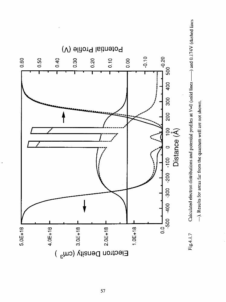
the I-V characteristic is shown in the insert. Shown in Fig. 4.1.7 are examples of electron
distributions and potential profiles obtained from self-consistent calculations (at V=O and
0.174V). Since C and G are derivative values, to obtain good and smooth C-V and G-V
curves we need very good results from self-consistent calculations. The calculation was
very time consuming. In this calculation we stopped the calculation before the
convergence reached our targeted limit, Because of this the calculated C-V and G-V
curves in Fig.4.1.6 are relatively rugged. However, they are good enough to show clear
peak features.
As mentioned in Chapter 3, our treatment does not include the scattering and
localization effects; also, the RTD operates far from thermal equilibrium but is considered
quasi-static. Similar to the I -V characteristics obtained from other quasi-static, non-
scattering self-consistent calculations, our result shows negative resistances; but when
compared to the experimental ones, the peak to valley ratios are higher. It was expected
that this calculation would provide only a qualitatively correct C-V picture. From
Figs.4.1.5 and 4.1.6 one can see that, except for the peak at the lower forward bias (at
V=O.lV and denoted by an arrow), the theoretically calculated C-V and G-V
characteristics agree qualitatively with the experimental results.


The theoretical C-V characteristic in Fig.4.1.6 shows that the capacitance peaks
are in fact located in the NDR regions. It is found that the NDR produces the most
dramatic change in charge distribution. When the RTD is pushed into the NDR region,
tunneling current decreases drastically and a large quantity of electrons transfer out of the
quantum well. The electron density in the well decreases sharply within a small increase in
applied voltage. Charge neutrality (the model used here is quasi-static) ensures that there
is also sharp increases in areas outside the quantum well. This rapid change in the electron
density distribution results in the peak (increase) in capacitance.
The capacitance peak is directly related to how many electrons are discharged
within a certain increase in voltage, associated with this discharging process is the negative
conductance. Typically the lower is the negative conductance peak the higher is the
capacitance peak. This can be seen by comparing the experimental and theoretical results
for the forward and reverse biases (Figs.4.1.5 and 4.1.6). Calculation shows that under
forward bias, electrons discharge from the quantum well much more drastic than that
under the reverse bias (that is, the number of electrons transferred out of the well within a
given change of bias is larger). Reflected in the I-V characteristic is that the negative
conductance in forward bias is much larger (Fig.4.1.6). Because the discharging process in
the forward bias is far more drastic, the forward bias capacitance peak is much larger than
the reverse bias one.
Under forward bias, there is an additional peak in the calculated C-V curve at
V=O. 1V (Fig.4.1.6, denoted by an arrow). It occurs during the quantum well charging
process and coincides with a positive conductance peak. It is much s-ml.ler than the
discharging one. In reverse bias no similar feature is observed. Our calculation indicates
that discharging processes are much faster than charging processes. Reflected in the I-V
characteristic is that the negative conductance peak (in NDR region) is much larger than

the positive one. In the reverse bias the change in charge distribution is relatively small,
and the capacitance peak induced by the charging process is so small that it is not visible in
Fig.4.1.6. In the experiment, both charging peaks are very shallow (see dldV in
Fig.4. IS), and the charging induced capacitance increases for the forward and reverse
biases are invisible.
Compared to the forward bias, the calculated C-V characteristic at the reverse bias
is closer to the experimental one, both in shape and value. Calculation indicates that, under
forward bias electrons charge and discharge from the quantum well much faster than that
under the reverse bias. Capacitance peaks in the forward bias are thus much larger than
the reverse bias ones, especially the discharging one. Quantitatively, the calculated
capacitance at zero bias (0.19pF) is about twice the measured value (0.09pF). The
experimental capacitance peak in the reverse bias is 0.1 lpF, about one third of the
theoretical 0.33pF. The peak in the forward bias is 0.12pF, much smaller than the
theoretical 8.6pF. The charging peak in the forward bias is not observed in experiment.
For the I-V curve, theoretical peak voltages (Vpead are smaller than the experimental ones
(-0.43V and 0.17V compared to -0.45V and 0.39V). Peak to valley ratios are larger and
negative differential conductances are much larger. These discrepancies are believed to
have resulted from the quasi-static and non-scattering approximations in our calculation. It
is known that the RTD operates far from equilibrium and scattering is always a very
important factor in device transport (Kluksdahl et al., 1989; Frensley, 1990). Considering
the RTD as non-equilibrium and including the scattering effects may raise the potentials on
undoped spacer layers, and increase the calculated NDR (or Vpeak) to a more reasonable
voltage. Studies on I-V characteristics have suggested that scattering can drastically
reduce the peak-to-valley ratio and negative conductance in the NDR region (Frensley,
1990; Hu and Stapleton, 1991). If scattering and localization effects are taken into

consideration (which will very much complicate the calculation), we expect that electrons
will move less freely and the change in electron density will be less sigdicant,
consequently dQ and capacitance will be smaller and more appropriate peak values will be
obtained. With scattering effects we also expect the charging peak in the forward bias to
be reduced, just as that observed in the experiment.
Cutof Frequency
, There have been many high speed applications for RTDs. Among them are high
frequency mixers and multipliers which utilize the non-linearity of the conductance or
capacitance. For mixers and multipliers that utilize the voltage variable capacitance
property (varactor property), a rapid change in capacitance is desired, as it can result in a
stronger nonlinearity, and subsequently in higher conversion efficiency and lower loss
(MacPherson, 1957; Uenohara and Gewartowski, 1969). Our result shows that generally a
rapid change in capacitance can be obtained by increasing the negative resistance or the
peak to valley ratio, which has been the objective pursued by many researchers since the
invention of the RTD. There have been many successful efforts in increasing the peak to
valley ratio (for example, see Sze, 1990). Certainly these methods are also applicable to
optimize the structure for varactor mixer and multiplier applications.
The cutoff frequency fc has always been considered one of the criteria for high
frequency performance. It is defined as the maximum frequency the device can produce
gain. Below fc the real part of the impedance Re(2) is negative and above fc Re(Z) is
positive. For the Esaki equivalent circuit in Fig.l.l.2, the cutoff frequency is obtained
from Re(Z(f,))=O:
2 n c

Eq.(4.1.2) suggests that, to obtain a high fc, we need a large G (negative value) and a
small C. For most high frequency applications, a higher cutoff frequency is desired and a
lower capacitance is wanted. In most RTD applications, the device is operated in the NDR
region. Our result shows that capacitance increases in the NDR region, therefore to obtain
a higher cutoff frequency, the capacitance peak must be reduced.
Since the results from the small signal equivalent circuit in Fig. 1.1.2 agree very
well with experiment up to 18GHz, it is expected to be applicable at higher frequencies. f,
under reverse bias has been calculated with Eq.(4.1.2) and the maximum fc is found to be
49GHz for the diode. The maximum fc is obtained at the conductance and capacitance
peak voltage (V=-0.49V), at which we have a minimum G=l/Rd=-0.0051R and a
maximum C=O.l lpF. The corresponding forward bias maximum fc is 35GHz, obtained at
V=0.41V (G=-0.004Q and C=O. 12pF). The cutoff frequency is higher in the reverse bias,
as the negative conductance is larger and the capacitance is lower. Furthermore, if we
consider the theoretical result in Fig.4.1.6, we will see that even though the negative
conductance is higher under forward bias, the cutoff frequency is still lower. The increase
in capacitance has offset the advantage of the higher negative conductance. This will be
more clearly seen in our experimental result from MAS-GaAs diodes with a similar
structure (section 4.3).
Obviously, further reductions in capacitance and parasitic resistance are necessary
to increase the cutoff frequency. Our result shows that in the reverse bias, the capacitance
is lower. If we compare the diode structures in two different biases, we will see that, under
reverse bias the diode has a longer anode spacer layer (due to the asymmetry of spacer
layer). So increasing the anode spacer layer could be one of the possible solutions for
obtaining a high cutoff frequency. We will see that, our following experimental and
theoretical results all support this suggestion.

4.2 Impedance, Equivalent Circuit and C-V Characteristics: A10.4Ga0.6As-GaAs
Diode, up to 40GHz
The structure of this diode is the same as the above one, however the diode area is
7 ~ 7 ~ m 2 . The dc I -V characteristic for the diode is shown in Fig.4.2.1. In the NDR region
some irregular jumps were observed. The diode had a larger peak to valley ratio compared
to the diode in section 4.1. It exhibited much stronger oscillations due to the larger
negative conductance. Oscillations in the NDR region were believed to be responsible for
the irregular jumps in the I-V curve which were not observed in the diode in section 4.1.
In S parameter measurements, to reduce the parasitic effects, we positioned the
probes as close as possible to the diode. Compared to the I-V measurement, S parameter
measurements give much more stable results in the NDR region, especially at the higher
frequencies. Stable S parameter measurements could be obtained because of two reasons:
1) The 5OQ external impedance presented to the diode by the network analyzer
significantly decreases the oscillation amplitude. 2) At higher frequencies the input signals
period is a few orders of magnitude smaller than the oscillation period. As the oscillation
magnitude was not very large (-15mVpp), its effect on the S parameter is considered not
significant.
As examples, Figs.4.2.2(a) and (b) show the measured impedances at V=OV and
-0.5 1V. Also shown are values calculated from the Esaki equivalent circuit description in
Fig. 1.1.2. Over the entire bias range (-0.7 to 0.55V), with Ls=2 lpH and R,=6.l rR, good
agreements can be obtained between calculated and experimental results. In this case L, is
comparable to that of the short-circuited reference devices, indicating that it is a result of
the connecting air-bridge and probe pads. This again enforces the argument that the active
RTD structure is represented by the G-C plus R, structure. By fitting the measured results

App
lied
volta
ge (
V)
Fig
.4.2
.1
Mea
sure
d I-
V ch
arac
teri
stic
for
the
RT
D (
solid
line
). T
he d
ashe
d lin
e is
obt
aine
d by
int
egra
ting
the
G-V
curv
e fr
om R
F m
easu
rem
ents
in F
ig.4
.2.3
.

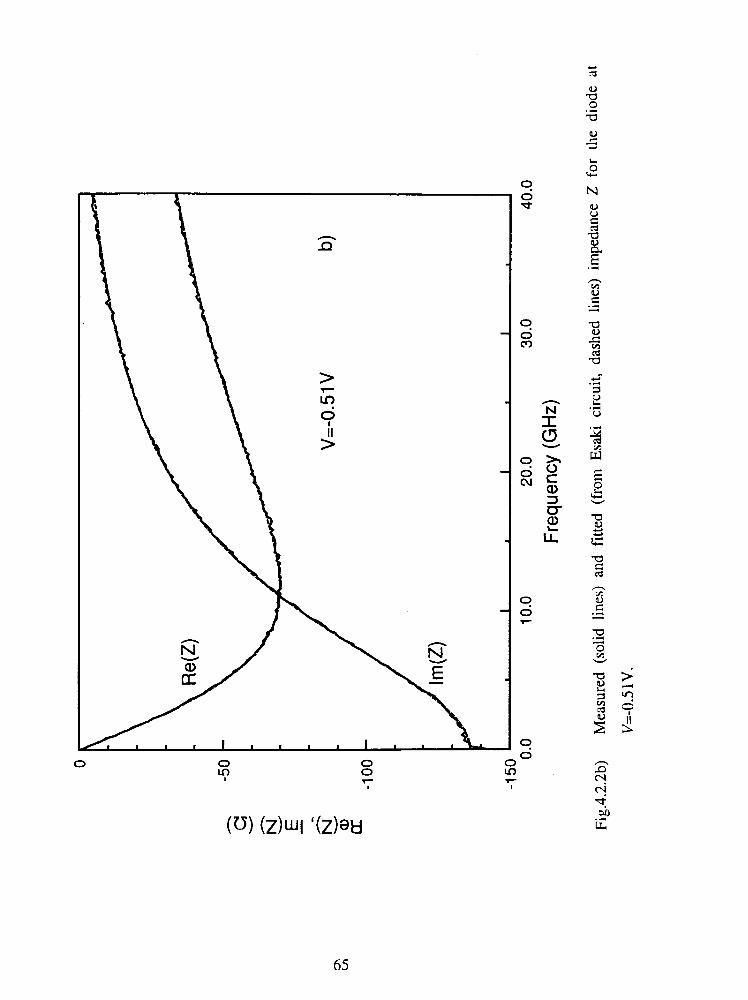

with the equivalent circuit, C-V and G-V characteristics for the diode are obtained and
plotted in Fig.4.2.3.
The agreements seen in Fig.4.2.2 between experimental and predicted curves
demonstrate the validity of the Esaki equivalent circuit model up to 40GHz. Since the
agreements between predicted and experimental results are good, it is expected that the
equivalent circuit model is valid to frequencies in excess of 40GHz, and can be reliably
used for microwave circuit designs and simulations.
No hysteresis but some irregular jumps were observed in the I-V characteristic
(Fig.4.2.1). We believe that they were the results of oscillations that were present in the
NDR region. Simulations have suggested that in a dc I-V measurement, due to the
recWied oscillatory current, the measurement can exhibit small jumps or hysteresis
(Okean, 1971; Liu, 1988; Belhadj et al., 1990). In this diode, low frequency oscillations
were observed in NDR regions during the measurement and jumps were found in the I-V
characteristic. On the other hand, the conductance G (which is (m//dl-~,)-l) obtained
from S parameter measurements was smooth, and no jump was observed (Fig.4.2.1). By
integrating the G-V curve in Fig.4.2.3 (R, is much smaller than dVldl and is neglected
here), a smooth I-V curve has been obtained and is shown as the dashed line in Fig.4.2.1.
The integrations are performed only over the distorted portions, that is, the integrals start
at the ends of the smooth measured curve. Since the smooth dashed curves are obtained
without severe oscillation interference, we believe they represent the intrinsic I-V
characteristic in the NDR regions. The recovery of the I -V curve demonstrates that with
high frequency impedance measurements, low frequency-low power oscillations can be
ignored and meaningful electrical characteristics can be extracted.
The C-V characteristic of the diode is shown in Fig.4.2.3. It is very similar to that
obtained from the diode in section 4.1. It shows two electron discharging peaks in two

Conductance ( 0 -I)
NDR regions. One can see that, similar to the above diode, the capacitance in the reverse
bias is lower than that in the forward bias. The highest cutoff frequencies obtained for
forward and reverse bias directions are 54GHz (at V=-0.51V) and 41GHz (at V=0.36V),
respectively.
4.3 Impedance, Equivalent Circuit and C-V Characteristics: AIAs-GaAs Diode: up
to 40GHz
The area of this diode is 7f lpm2 and its structure has been illustrated in Fig.2.1.2.
The I-V characteristic for the diode is shown in Fig.4.3.1. A strong hysteresis was
observed in the reverse I-V characteristics, in the forward bias a very weak hysteresis was
also observed. Due to the asymmetry in spacer layers, the obtained I-V characteristic was
asymmetric. Onset of the NDR region (Vpenk) occurred at a lower voltage in the forward
direction. This was due to the fact that the anode undoped spacer layer is 100A and the
cathode spacer layer is 700A (Fig.2.1.2). An inflection which was not observed in
A ~ O . ~ G ~ ~ . ~ A S - G ~ A S diodes was found in the forward bias at 0.6V. This structure has been
observed in some other RTDs with long cathode spacer layers (Paulus et al., 1990;
Mounaix et al., 1990). It was attributed to the quasi-bound state formed in the triangular
well in the cathode spacer layer adjacent to the barrier.
During microwave measurements, under forward bias, strong oscillations were
detected in the NDR region and data at lower frequencies was erratic. On the other hand,
the magnitude and phase of higher frequency data was stable and smooth. As with the
above diodes, when lower frequency data was not available because of the poor phase
locking of the network analyzer, measurements were extrapolated from more reliable
results obtained at higher frequencies. Under reverse bias conditions, the oscillations were
found to be much weaker. Contrast to that in the forward bias, in reverse bias, S
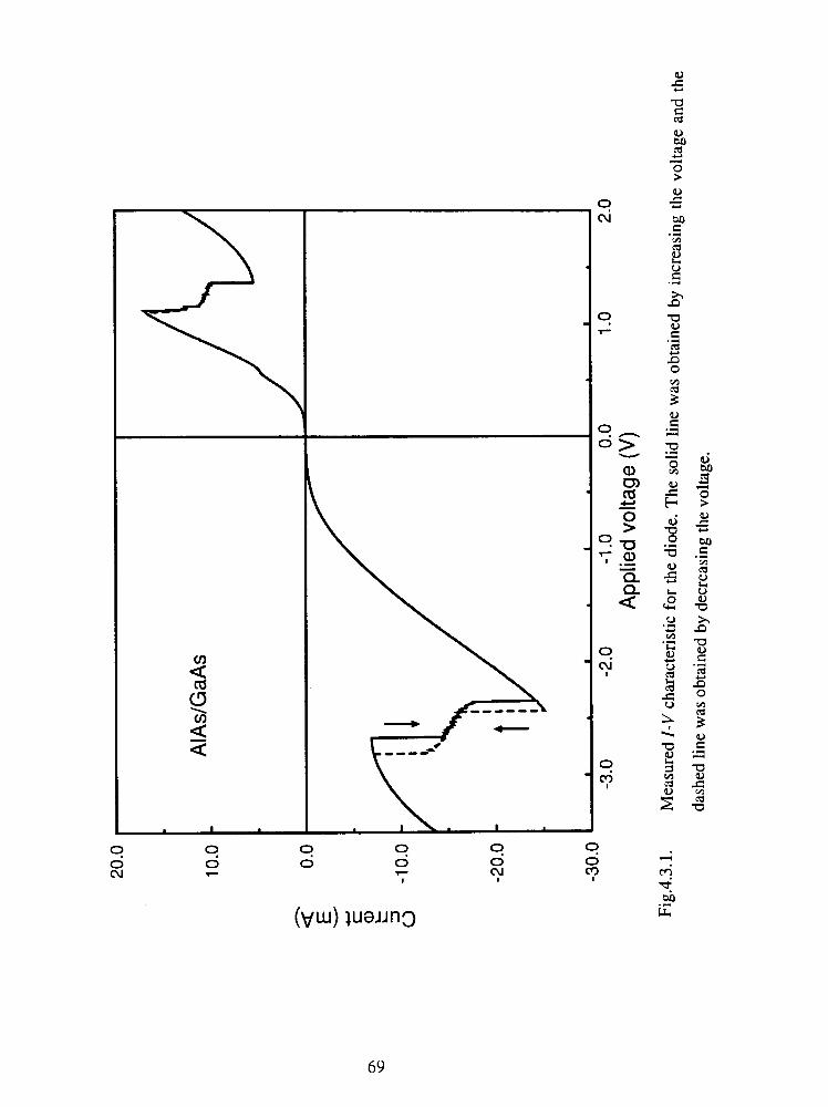
-2.0
-1
.o 0.
0 A
pplie
d vo
ltage
(V
)
Mea
sure
d I-
V ch
arac
teri
stic
for
the
diod
e. T
he s
olid
line
was
obt
aine
d by
incr
easin
g th
e vo
ltag
e an
d th
e
dash
ed li
ne w
as o
btai
ned
by d
ecre
asin
g th
e vo
ltage
.

parameter measurements were almost unaffected by oscillations. A hysteresis was
observed in these clean S parameter measurements in the reverse bias. For this diode
which had a wide bias range (-3.W to 2.5V), it was found that, different fiom the above
RTDs, to obtain a good fit between measured impedances and the equivalent circuit in
Fig. 1.1.2, series resistance R, had to be made a function of voltage. With inductance
Ls=5pH, R, was found to increase from about 6R near V=-3V to about 16R around
V=l SV. Shown in Fig.4.3.2 are examples of measured and fitted impedances (V=OV and
-2.64V). Obviously, the agreement between experimental and modeled results was quite
good, demonstrating the validity of the equivalent circuit up to 40GHz. Fig.4.3.3 shows
the modeled C-V and G-V characteristics.
Hysteresis
The hysteresis observed in S parameter measurements under reverse bias
conditions can also be seen in the C-V and G-V characteristics in Fig.4.3.3. The hysteresis
was originally observed in I-V measurements and attributed to the charge storage
mechanism (Goldman et al., 1987). However, some authors pointed out that the self-
oscillations could also lead to a similar phenomenon (Sollner, 1987; Liu, 1988; Belhadj et
al., 1990). The hysteresis observed in our impedance measurement was different fiom the
one resulting from oscillations, which showed a two step process like that in the I-V
characteristic in Fig.4.3.1. Since the impedance data in the reverse bias was obtained
without the interference of oscillation, we believe the hysteresis was intrinsic and not from
the oscillation.
There were studies that suggested the hysteresis might be a result of the internal or
external resistances of the device (Chow, 1964; Okean, 1971; Jogai, and Koenig, 1991;


Conductance (R -I)

Chen et al., 1991). Due to the fact that the peak current of the RTD is higher than the
valley current, the voltage drop on the series resistance at the peak voltage Vpeak is higher
than that at the valley voltage Vvalley If the resistance is not very small, the measured
peak voltage Vpeak, which is the "intrinsic" RTD voltage Vpeak plus the resistance
voltage, can be higher than the measured valley voltage V;alley (Fig.4.3.4), resulting in a
bistability (load-line bistability). From Fig.4.3.4, one can see that the range of such a
bistability is
Vl-h=Vl+Il (Rs+Rload)-V2-I2(Rs+Rload) (4.3.1)
where Rload is the external load-line resistance. Although V1, V2, Il and I2 are unknown
parameters, we know that Vl-V2<0, 11-Ipeak and 12-Ivalfey. If we approximate Il and 12,
respectively, by Ipeak and Ivalley, and taking the fact that the series resistance Rs is
voltage-dependent, we have
Vl~C"2~peak(Rs,peak+Rload)~zvalley(Rs,valley~Rload~ (4.3.2)
For this U S - G ~ A s diode, we have Rs,peak=12Q and Rs,varrey=8Q from
impedance measurements. With the measurement result of Rload=0.8Q, the right hand side
of Eq.(4.3.2) gives rise to 290mV, which is slightly larger than the 260mV hysteresis
observed. So the hysteresis has been a result of the load-line bistability. Here Rload is very
small, the hysteresis thus is mainly due to the internal series resistance R,. Similar
hysteresis phenomena were also observed in other AlAs-GaAs diodes, however, the
hysteresis and series resistance were all smaller than that of this one. We do not exclude
the possibility that there exists charge storage hysteresis, since the existence of such a
hysteresis has been supported by theoretical calculations (Kluksdahl et al., 1989).
However, to distinguish it from the load-line bistability, great care must be taken.

4
load
v peak
v
V'
V'
valle
y va
lley
peak
Fig.
4.3.
4 Sc
hem
atic
dia
gram
of
load
-lin
e bi
stab
ility
of
RT
D.
The
sol
id l
ine
is t
he "
intri
nsic
" I-
V c
urve
of
an i
deal
RT
D (
with
zer
o se
ries
res
ista
nce
R,)
. T
he d
ashe
d lin
e is
the
rea
l I-
V c
hara
cter
istic
whi
ch i
nclu
des
the
volt
age
drop
s on
the
R,
and
load
res
ista
nce
RlO
ad. B
ecau
se s
ectio
n A
'-B'
is u
nsta
ble,
dur
ing
the
I-V
mea
sure
men
t we
obta
in C
'-A'-D
' w
ith i
ncre
asin
g bi
as a
nd D
'-B'-C
' w
ith d
ecre
asin
g bi
as.

C-V Characteristic and Cutof Frequency
To simulate the C-V characteristic, we calculated the diode capacitance through
self-consistent calculations; but this time only under the forward bias (because the self-
consistent calculations were very time consuming). In the calculation, the barrier height
was assumed 1.1V (Batey and Wright, 1986). The calculated C-V and G-V (G=dldV)
characteristics for the diode in forward bias are plotted in Fig.4.3.5. In the insert the I-V
characteristic is also shown. The I-V curve shows a NDR and an inflection, very similar to
that observed in the experiment. However, the peak to valley ratio and bias magnitudes
are quite different. Fig.4.3.6 shows the calculated electron density distribution and
conduction band potential at V=0.09V, just before the inflection of the I-V characteristic.
The C-V characteristic obtained from rf measurements (Fig.4.3.3) shows that,
under forward bias, the capacitance increases with increasing voltage and then decreases,
followed by a peak that coincides with the inflection in the I-V characteristic and a larger
peak in the NDR region. The calculated C-V characteristic also demonstrates the same
behavior (Fig.4.3.5). However, both capacitance magnitudes and bias voltages are quite
different. The calculated inflection in the I-V characteristic is at 0.09V, and the NDR
begins at 0.14V, both are much lower than the experimental 0.9V and 1.14V. The peak to
valley ratio is also higher: 10 versus 3. Around V a V , the calculated capacitance is about
twice the measured value. AU capacitance and conductance peaks are higher than
experimental ones. The reason is that scattering was not included in the self-consistent
calculation. Except for the magnitudes, the calculation agrees qualitatively with the
experiment.
Here, the capacitance peak in the NDR region is again observed (Fig.4.3.3). We
know that the NDR peak is directly associated with the discharging process and the
negative conductance peak, typically the lower is the negative conductance peak the

+ I
0.20
A
pplie
d V
olta
ge (
V)
Fig.
4.3.
5 C
alcu
late
d C
-V (
solid
lin
e) a
nd G
-V (
dash
ed l
ine)
cha
ract
eris
tics
for
the
diod
e un
der
forw
ard
bias
. T
he
inse
rt s
how
s th
e ca
lcul
ated
I-V
cha
ract
eris
tic.
The
C-V
and
G-V
cur
ves
are
rela
tivel
y ru
gged
bec
ause
the
conv
erge
nce
lim
it fo
r th
e se
lf-c
onsi
sten
t cal
cula
tion
was
not
ver
y sm
all.

Electron density (1 0 "lcm 3 ,

higher is the capacitance peak. This can be seen quite clearly by comparing the
experimental results for forward and reverse biases (Fig.4.3.3). Under forward bias, the
negative conductance peak is lower and the capacitance peak is larger.
The capacitance peak at lower voltage is related to the inflection in the I-V
characteristic. Calculation shows that, band bending in the cathode spacer layer forms a
triangular well outside the emitter barrier. Like in the quantum well, a certain quasi-bound
state El is formed (Fig.4.3.6): at El tunneling probability attains one maximum. El is lower
in energy than the quasi-bound state E, in the well which is responsible for the usual
tunneling and the NDR. Due to the presence of El, there is an electron accumulation near
the emitter barrier outside the quantum well. The inflection in current is due to the
tunneling through El (Paulus et al., 1990; Mounaix et al., 1990). Associated with the
diminish of this tunneling is an electron discharging process that causes a rapid change in
charge distribution and the capacitance peak. In the reverse bias condition, because the
emitter spacer layer is shorter and the triangular well is very shallow, no similar
capacitance peak were observed.
Although the calculated capacitance agrees qualitatively with experimental results,
the differences in magnitudes are quite large. We again attribute these discrepancies to the
quasi-static and non-scattering approximations in our self-consistent calculations.
Experimentally, for this diode, the highest cutoff frequencies obtained for the two
bias directions are 60GHz (at V=-2.6V) and 41GHz (at V=1.31V). The highest f, we
obtained for same wafer was IOSGHz, from another 7 ~ 7 ~ m ~ diode and also in the reverse
bias (this diode exhibited much stronger oscillations and was less stable). The cutoff
frequency is higher under the reverse bias, because the capacitance is lower (Fig.4.3.3).
The reason the capacitance is lower is that, under the reverse bias the anode spacer layer is
longer. It is interesting to note that, for this diode, while the negative conductance in

forward bias is slightly higher, the cutoff frequency is still lower than that of reverse bias.
The same result was also found for other diodes with the same structure. In the forward
bias, although some of these diodes had a negative conductance peak that was almost
twice that in the reverse bias, f, obtained from the reverse bias was still higher than that
from the forward bias. The increase in capacitance and resistance have offset the
advantage of the larger negative conductance. As has been mentioned in sections 4.1 and
4.2 (and will be stipulated in section 4.4), for a RTD with similar asymmetric spacer layer
structure (with a longer anode spacer layer under reverse bias), the theoretical cutoff
frequency in the forward bias is lower than that in the reverse bias because of the higher
capacitance. The experimental results certainly support this argument. The reason that the
capacitance is lower under reverse bias is that the anode spacer layer is longer. Thus, to
increase the cutoff frequency for high speed applications, a longer anode spacer layer
should be used (assuming transit time effect is still negligible).
4.4 Effects of Spacer Layers on C-V Characteristic: Theoretical Considerations
We have investigated the effects of spacer layers on capacitance, by studying four
different RTDs with unit areas. The central parts of all these RTDs are an identical 4081-
50A-40A barrier-well-barrier quantum well structure. The spacer layers on one side of the
quantum well are IOOA, on the other side they are 100A, ~ooA, 700A and 1000A,
respectively. The barrier height is 0.22V, resembling that of an A ~ o ~ G ~ o J A s - G ~ A s RTD.
The electron concentrations of both contact layers are 2x10~8 cm-3. The temperature is
300K. For convenience, we define the 100A side as positive. That is, under forward bias,
the anode spacer layer is fixed as 10081 and the cathode spacer layer varies from 10081,
30081, 70081 to 100081; under reverse bias it is the opposite, the cathode spacer layer is
fixed and the anode spacer layer varies. The effects of cathode and anode spacer layers on

the capacitance can be respectively studied by studying the capacitance under two
different directions.
As was pointed out in sections 4.1 and 4.3, due to the lack of scattering, calculated
C-V characteristics agree only qualitatively with experimental ones. Despite the limitation,
we expect that the calculations to still provide a correct dependency on how the
capacitance varies with spacer layer. We believe this tendency will not be altered by the
introduction of scattering. That is, our results can be used as a guideline for optimizing the
structure of a RTD.
The calculated current density-voltage characteristics for four diodes are shown in
Fig.4.4.1. Under forward bias, magnitudes vary greatly, peak to valley ratios are 3.1: 1 for
the 100A diode and about 10:l for three others. In the reverse bias the peak voltage
increases with increasing anode spacer layer. Although the current magnitude for the
l00a is slightly lower, the peak to valley ratios are quite close for all four (-3: 1).
The specific capacitances for forward and reverse biases are shown in Figs.4.4.2
and 4.4.3, respectively; also shown are the conductances which are the derivatives of the
I-V curves. The common feature for all these diodes is the electron discharging peak in the
NDR region, in both positive and negative biases.
Under forward bias, the discharging capacitance peaks are very high for the 300A,
700A and 1000A diodes. It is interesting to see that, the peak increases greatly when the
cathode spacer layer is increased from l00A to 300A, when the spacer layer is increased
further to l000A it decreases (Figs.4.4.2 and 4.4.3). The calculations show that the
capacitance peak height depends strongly on the discharging process, which in turn,
depends partially on the negative conductance peak in the NDR region. The 300A diode
has the largest negative conductance peak and it has the highest capacitance peak. It is
found that, changes in I-V characteristic and electron density in the well are primarily


0.0
0.2
0.4
0.6
0.8
1.0
App
lied
Vol
tage
(V
)
Fig
.4.4
.1 b)
C
alcu
late
d re
vers
e bi
as c
urre
nt d
ensi
ty-v
olta
ge c
hara
cter
istic
s fo
r R
TD
s w
ith u
nit
area
s. T
he c
atho
de
spac
er la
yer i
s 10
0A. T
he a
node
spa
cer
laye
rs a
re l
00A
(sol
id li
ne,
), 30
0A (
dash
ed li
ne, - - - -)
,
700A
(dot
ted
line,
-.-.-.
) an
d l0
00A
(do
t lin
e, --
-).

I I
- 1 0 . 0 ' - " ' - " " ' - ' - 0 0.02 0.04 0.06 0.08 0.1 0.12 0.14
Applied Voltage (V)
Fig.4.4.2 a) Calculated specific C-V characteristics for three diodes under forward
bias. The undoped cathode spacer layers are 300A (dashed line, - - - -),
700A (dash-dotted line, ---) and l000A (dotted line, ......-... ). b) The
corresponding conductances for the diodes. The results for the 100A diode is
symmetric and shown in Fig.4.4.3.

Applied Voltage (V) a) Calculated specific C-V characteristics for diodes under reverse bias. The
undoped anode spacer layers are ~ O O A (solid line, ), 300A (dashed
line, - - - -1, 700A (dash-dotted line, ------) and l000A (dotted line,
.......... ). b) The corresponding conductances for the diodes.

determined by the charge distribution in the emitter (cathode) area. Increasing the spacer
layer from l0OA to 300A reduces the cathode electron density. When the cathode density
is low and if the diode is biased into the NDR region, quantum well density and current
decreases sharply. Increasing the spacer layer further to 700A and IOOOA, the electron
density in the cathode spacer layer increases, bending the potential near the upper barrier
(Fig.4.4.4). The result is that, decreases in current and quantum well electron density are
slightly less significant. Consequently the negative conductance and capacitance peaks are
smaller.
Under reverse bias, the capacitance peak decreases and broadens slightly with
increasing anode spacer layer. The change in the peak is relatively small compared to that
under the forward bias. This is because the charge distribution in the cathode, by which
the discharging process is mainly determined, is affected relatively little by the variation in
anode spacer layer. On the other hand, in both forward and reverse biases, the capacitance
decreases as a whole with increasing spacer layer (this can be seen more clearly in
Fig.4.4.3 for the reverse bias), as the undoped space between the two contacts increases.
Except for the increases in NDR regions, there is an additional capacitance peak in
the forward bias at lower voltage (Fig.4.4.2). This peak is quite high for the l000A diode,
it is smaller in the 700A diode, and in the 300A diode it is invisible. This peak is a result of
the quantum well charging process which occurs during tunneling. It coincides with a
positive peak in the conductance. During the tunneling process, electron density in the
quantum well increases rapidly with increasing applied voltage, associated with this
increase is a rapid variation in electron density distribution and a peak in the capacitance.
The charging processes in the l000A and 700A diodes are more prominent than that in the
100A and 300A diodes, consequently larger changes in the electron distributions and
higher capacitance peaks are resulted. In the reverse bias the charging process is relatively


slow compared to the forward bias, therefore no such increase is observed. This peak has
never been observed in experiments. Similar to the peaks in the NDR regions, in a real
device it is believed to be reduced and broadened by scattering effects.
The calculations for the reverse bias show that, changing the anode spacer layer
does not significantly affect the peak in the NDR region. But in general, increasing the
anode spacer layer results in a decreasing capacitance. However, the peak is quite
sensitive to the variation in cathode spacer layer. Increasing the cathode spacer layer could
cause the capacitance peak to increase.
For varactor mixer and multiplier applications, to obtain high conversion efficiency
and low loss, a rapid variation which results in a strong nonlinearity in capacitance is
desired (MacPherson, 1957; Uenohara and Gewartowski, 1969; Roddy, 1986). In these
cases a longer cathode spacer layer should be used. For oscillators and logic circuits,
lower capacitance is usually needed as higher cutoff frequency is normally desired. To
obtain a high cutoff frequency a larger negative admittance and a lower capacitance are
desirable. Assuming that the series resistivity has a typical value of 5 ~ 1 0 - ~ ~ c m - ~ , one can
show that for the 700A diode, the maximum cutoff frequencies (obtained at the minimum
negative conductances) are 260GHz and 1.1THz for forward bias and reverse bias,
respectively. It is again interesting to see that although the negative conductance in
forward bias is larger, the cutoff frequency is in fact lower. Similar results can be also
obtained for three other diodes. This agrees with our experimental results for diodes of
similar spacer layer structures shown in sections 4.1, 4.2 and 4.3. The advantage of the
increasing negative conductance has been reduced by the higher capacitance. This also
suggests that the spacer layer does play an important role in diode n&x~wave
characteristics and applications.

Since the invention of the RTD, numerous researches have been conducted to
obtain higher negative conductance, or higher peak to valley ratio (for example, see Sze,
1990). Our result indicates that, the effect of the increase in capacitance brought on by
increasing the negative conductance can be negative for some applications (for example
oscillators), as the cutoff frequency is reduced. There is a tradeoff between capacitance
and negative conductance in obtaining a higher cutoff frequency. If we consider the
reverse bias cutoff frequencies for the 100A, 300A and l000A diodes, we will see that
they are 940GHz, 1.1THz and 1.4THz, respectively. So, as in sections 4.1, 4.2 and 4.3,
we find that, one choice for achieving a high cutoff frequency is to increase the anode
spacer layer.
4.5 Effects of Fixed Space Charge on I-V and C-V Characteristics: Theoretical
Considerations
The device under study is a 3G~.7As-GaAs RTD. The central part of the RTD
is an undoped ~ o A - ~ o A - ~ A barrier-guantum well-barrier structure. The barrier height is
0.22V. On both sides of the well-barrier structure are undoped spacer layers of 100A. The
whole structure is sandwiched by two n+-GaAs ( N ~ = ~ X I O ~ ~ cm-3) contact layers.
Assuming a fixed interface space charge density of u=5x10~0cm-~ (Kroemer et
al., 1980) at four heterojunctions (o is assumed not to change with voltage), the current
density and specific capacitance have been calculated. They are plotted in Figs.4.5.1 and
4.5.2, respectively. For comparison, results for o=O are also shown. Fig.4.5.1 clearly
indicates that the fixed space charge shifts the location of the current peak. However, the
peak to valley ratio is virtually unaffected and remains roughly 3.1: 1. Due the existence of
the fixed space charges at the interfaces, the potential around the quantum well area
decreases, along with this decrease is the quasi-bound state in the quantum well. The


decrease in the quasi-bound state results in a decrease in peak voltage Vpmk. The decrease
in the quasi-bound state also lowers the tunneling energy; thereby increasing the number
of electrons that can tunnel through the barriers, which in turn increases the peak current.
The peak to valley ratio is determined primarily by the width of the quasi-bound state, the
calculation shows that it is not substantially altered by the fixed space charge. For a fixed
interface space charge density which has resulted from defects in heterojunctions, the
value of 5 x l 0 ~ ~ c m - ~ is very typical (Kroemer et al., 1980). Our results thus show that,
like the unintentional background impurities (Wolak et al., 1988), the interfacial impurities
in a normal RTD are not sufficient to significantly degrade the I-V characteristic.
The effect of the fixed space charge on capacitance is more significant. Our
calculation shows that by including a fixed space charge of a=5x10~0cm-*, the
capacitance peak in the NDR region increases by about 10% (Fig.4.5.2).
Usually, when the capacitance increases, the performance of a device degrades. To
consider this degradation we calculate the difference in cutoff frequencies. The highest
cutoff frequency f,,,, is obtained when -G and C are at their maximums. For this RTD,
with a resistivity of 5x10⁻⁷Rcm-2, f,,,, can be found to decrease from 233GHz to
219GHz when we include the fixed interface charge. The decrease is about 6% and less
than the 10% change in capacitance. The reason is that the negative admittance value is
also slightly increased. Generally speaking, the degradation in the performance due to
fixed space charge is not very significant.

CHAPTER 5. CONCLUSIONS
Through on-wafer probing S parameter measurements, accurate small signal
impedances for RTDs up to 40GHz have been obtained. It has been found that the
impedances can be described by the Esaki equivalent circuit that consists of a parallel G-C
and a series R-L circuit. In the equivalent circuit, the inductance has been found to result
from the on-wafer connecting lines and the air-bridge structure. The quantum well itself
can be represented by the parallel G-C circuit alone. The series resistance is associated
with the contact and spreading resistance in the semiconductor. With measured
impedances, G-V and C-V characteristics have been obtained from the equivalent circuit
representation. The G-V characteristic is found to be comparable to that obtained from dc
I-V characteristic. With this oscillation-free rf G-V characteristic, portions of the I-V curve
that were distorted in dc measurements have been restored. A hysteresis that is not
affected by oscillations has been observed in impedance measurements. It is believed to be
intrinsic and not from oscillations. But it is due to the load-line bistability of internal series
resistance, rather than the charge storage effects predicted by theories.
Based on the charge distributions obtained from self-consistent calculations,
capacitances of RTDs have been calculated and compared to experimental results. The
calculated C-V characteristics are found to agree qualitatively with experimental ones.
Both the theoretical and experimental results exhibit a capacitance peak in the NDR
region. Calculations show that it is a result of the process of electrons discharging from
the quantum well, instead of the charge accumulation in the quantum well as was
previously believed. Also found is a smaller capacitance peak corresponding to electrons

discharging from the accumulation region in the undoped region adjacent to the emitter
barrier.
We have calculated the capacitance for RTDs with different spacer layers. The
effects of spacer layers on capacitance have been discussed. Calculations show that the
capacitance value decreases in general with increasing spacer layer. The anode spacer
layer has a relatively limited effect on the peak in NDR region compared to the cathode
spacer layer. The increase in the negative conductance is usually accompanied by an
increase in capacitance. Usually a high peak to valley ratio, or a larger negative
conductance, is desirable. Our studies indicate that, by varying the cathode spacer layer,
the negative conductance can be increased. However, increasing the negative conductance
also brings up the capacitance, and the net effect may be negative, as the cutoff frequency
is reduced. On the other hand, increasing the anode spacer layer can decrease the
capacitance in the NDR region and thereby increase the cutoff frequency of the RTD.
The effects of fixed interface space charge on I -V and C-V characteristics are
discussed. It is found that high frequency performance of the device will be degraded by
the f d space charge. However, for a fixed space charge density that has resulted from a
normal interface disorder, the effect is not very significant.

BIBLIOGRAPHY
P. D. Baelaan, and M. A. Frerking, 1987, "Quantum well multipliers", Dig. Twelfh Int.
Con$ Infrared and Millimeter Waves, pp. 14.
J. Batey, and S. L. Wright, 1986, "Energy band alignment in GaAs:(Al,Ga)As
heterostructures: The dependence on alloy composition", J. Appl. Phys., vo1.59,
pp.200-209.
C. Y. Belhadj, K. P. Martin, S. Ben Arnor, J. J. L. Rascol, R. J. Higgins, R. C. Potter, H.
Hier, and E. Hempfling, 1990, "Bias circuit effects on the current-voltage
characteristic of double- barrier tunneling structures: experimental and theoretical
results", Appl. Phys. Lett., vol. 57, pp.58-60.
D. J. BenDaniel and C. B. Duke, 1966, "Space-charge effects on electron tunneling",
Phys. Rev., vol.152, pp.683-692.
0. T. Boric, J. Tolrnunen, E. Kollberg, and M. A. Frerking, 1992, "Anomalous
capacitance of quantum well double-barrier diodes", Int. J. Infrared and
Millimeter Waves, vol. 13, pp.799-8 14.
E. R. Brown, T. C. L. G. Sollner, W. D. Goodhue, and C. D. Parker, 1987, Appl. Phys.
Lett., vo1.48, pp.422.
E. R. Brown, C. D. Parker, and T. C. L. G. Sollner, 1989, "Effect of quasibound-state
lifetime on the oscillation power of resonant tunneling diodes", Appl. Phys. Lett.,
vol54, pp.934-936.
E. R. Brown, T. C. L. G. Sollner, C. D. Parker, W. D. Goodhue, and C. L. Chen, 1989,
"Oscillations up to 420GHz in GaAs/AlAs resonant tunneling diodes", Appl. Phys.
Lett., vol. 55, pp.1777-1779.
M. Biittiker, 1986, Phys. Rev., vol. B33, pp.3020.

M. Cahay, M. McLeman, S. Bandyopadbyay, S. Datta, and M. S. Lundstrom, 1986,
"Self-consistent treatment of electron propagation in devices", in Simulation of
Semiconductor Devices and Processes, V.2, (Pineridge, Swansea).
F. Capasso, K. Mohammed, and A. L. Cho, 1986, "Resonant tunneling through double
barriers, perpendicular quantum transport phenomena in superlattices, and their
device applications", IEEE J. Quantum Electron., vol. QE22, pp. 1853- 1869.
F. Capasso, 1990, Physics of quantum electron devices, (Springer-Verlag, Berlin).
L. L. Chang, L. Esaki, and R. Tsu, 1974, "Resonant tunneling in semiconductor double
barriers", Appl. Phys. Lett., vo1.24, pp.592-595.
J. G. Chen, C. H. Yang, and R. A. Wilson, 1991, "On the intrinsic bistability in resonant
tunneling structures: observation of area dependance of hysteresis", J. Appl. Phys.,
v01.69, pp.4132-4134.
W. F. Chow, 1964, Principles of Tunnel Diode Circuits, (John Wiley & Sons, New York)
L. Eaves, M.L. Leadbeater, D.G. Hayes, E.S. Alves, F.W. Sheard, G.A. Toombs, P.E.
Sirnrnonds, M.S. Skolnick, M. Henini, and O.H. Hughes, 1989, Solid-state
Electron., vo1.32, pp. 1 101
W. R. Frensley, 1989, "Quantum kinetical theory of nanoelectronic devices (resonant
tunneling diode)", in Nanostructure Physics and fabrication, Proceedings of the
International Symposium, College Station, TX, 1989, edited by M. A. Reed and
W. P. Kirk (Academic, San Diego).
W. R. Frensley, 1990, "Boundary conditions for open quantum systems driven far from
equilibrium", Rev. Mod. Phys., vo1.62, pp.745-79 1.
J. Genoe, C. Van Hoof, W. Van Roy, J. H. Smet, K. Foebelet, R. P. Mertens, and G.
Borghs, 199 1, "Capacitances in double- barrier tunneling structures" , IEEE Trans.
Electron Devices, vo1.38, pp.2006-20 12.

J. M. Gering, D. A. Crirn, D. G. Morgan, P. D. Coleman, W. Kopp, and H. Morkoc,
1987, "A small-signal equivalent-circuit model for GaAs-A1,Gal-,As resonant
tunneling heterostructures at microwave frequencies", J. Appl. Phys., vo1.61,
p.27 1-276.
V. J. Goldrnan, D. C. Tsui, and J. E. Cuningharn, 1987, "Observation of intrinsic
bistability in resonant-tunneling structures", Phys. Rev. Lett., vo1.58, 1256-1259.
H. K. Gurnrnel, and D. L. Scharfetter, 1967, "Depletion-layer capacitance of p+n step
junctions" J. Appl. Phys., vo1.38, pp.2148-2153.
Y. Hu, and S. Stapleton, 1991, "Quantum capacitance of resonant tunneling diodes",
Appl. Phys. Lett., ~01.58, pp. 167- 169.
Y. Hu, 1991, unpublished research report, School of Engineering Science, SFU.
J. D. Jackson, 1975, Classical Electrodynamics (John Wiley & Sons, New York).
C. Jacoboni, and P. Lugli, 1989, The Monte Carlo Method for Semiconductor Device
Simulation (Springer-Verlag, Wien).
B. Jogai, and E. T. Koenig, 1991, "A parametric study of extrinsic bistability in the
current-voltage curves of resonant tunneling diodes", J. Appl. Phys., vo1.69,
pp.338 1-3383.
D. P. Kennedy, P. C. Murley, and W. Kleinfelder, 1968, "On the measurement of impurity
atom distributions in Silicon by the differential capacitance technique", IBM J. Res.
Develop., vol. 12, pp.399-409.
V. P. Kesan, D. P. Neikirk, P. A. Blakey, B. G. Streetman, and T. D. Linton Jr., 1988,
"The influence of transit-time effects on the optimum design and maximum
oscillation frequency of quantum well oscillators", IEEE Trans. Electron Devices,
vo1.35, pp.405-413.

V. P. Kesan, A. Mortazawi, D. R. Miller, V. K. Reddy, D. P. Neikirk, and T. Itoh, 1989,
"Microwave and milimeter-wave QWITT diode oscillators", IEEE Trans.
Microwave Theory Tech. vo1.37, pp. 1933- 1940.
N. C. Kluksdahl, A. M. Krirnan, D. K. Ferry, and C. Ringhofer, 1989, "Self-consistent
study of the resonant-tunneling diode", Phys. Rev., vol.B39, pp.7720-7735.
K. Krishnarnurthi and D. R. Conn, 1991, "Conversion gain and stability of a resonant
tunneling diode harmonic mixer", Microwave and Optical Tech. Lett., vol. 4,
pp.212-216.
H. Kroemer, Wu-Yi Chien, J. S. Harris Jr., and D. D. Edwall, 1980, "Measurement of
isotype heterojunction barriers by C-V profiling", Appl. Phys. Lett., vo1.36, pp.295-
297.
R. Landauer, 1970, Philos. Mag., vol. 21, pp.863.
J. M. Langer, C. Delerue, M. Lamoo, and H. Heinrich, 1988, "Transition-metal impurities
in semiconductors and heterojunction band lineups", Phys. Rev., vol.B38, pp.7723-
7739.
D. Lippens and P. Mounaix, 1988, "Small-signal impedance of G ~ A S - A ~ , G ~ ~ _ ~ A S
resonant tunneling heterostructures at microwave frequency", Electron. Lett.,
~01.24, pp. 1 180- 1 18 1.
H. C. Liu, 1988, "Simulation of extrinsic bistability of resonant tunneling structures",
Appl. Phys. Lett. vol. 53, pp.485-486.
A. C. MacPherson, 1957, IRE Tram. Microwave Theory Tech., vol.MTT-5, pp.43.
R. E. Miles, G. Millington, R. D. Pollard, D. P. Steenson, J. M. Chamberlain, and M.
Henini, 1991, "Accurate equivalent circuit model of resonant tunneling diodes",
Electron. Lett., vo1.27, pp.427-428.

G. Millington, R. E. Miles, R. D. Pollard, D. P. Steenson, and J. M. Chamberlain, 1991,
"A resonant tunneling diode self-oscillating mixer with conversion gain", IEEE
Microwave and Guided Wave Lett., vol. 1, pp.320-32 1.
A. Mortazawi, V.P. Kesan, D.P. Neikirk, and T. Itoh, 1989, "A self-oscillating QWITT
diode mixer", in Proc. 19th European Microwave Conf. Sept. 1989, pp.7 15.
P. Mounaix, 0. Vanbesien, and D. Lippens, 1990, "Effect of cathode spacer layer on the
current-voltage characteristics of resonant tunneling diodes", Appl. Phys. Lett.,
~01.57, pp.1517-1519.
H. C. Okean, 1971, "Tunnel diodes", in Semiconductors and semimetals, vo1.7, part B, R.
K. Willardson and A. C. Beer Eds., (New York, Academic).
M. J. Paulus, E. T. Koenig, B. Jogai, C. A. Bozada, C. I. Huang, C. E. Stutz, and K. R.
Evans, 1990, "Effects of low-doped spacer layer in the emitter of a resonant
tunneling diode", Superlatt. Microstruct., vo1.7, pp 135- 137.
A. Raychaudhuri, and M. J. Deen, 1993, "New static storage scheme for analogue signals
using four-state resonant-tunneling devices", Electron. Lett., vo1.29, pp.1435-
1437.
D. Roddy, 1986, Microwave Technology, Englewood Cliffs, (New Jersey, Prentice-Hall).
C. V. Sammut, N. J. Cronin, R. D. Schnell, and H. Tews, 1993, "Accurate small-signal
modeling of a double barrier resonant tunneling diode (DBRTD)", IEEE M T - S
Digest, pp. 104 1- 1044.
M. F. C. Schemmann, H. C. Heyker, J. J. M. Kwaspen, and Th. G. van de Roer, 1991,
"Microwave impedance measurements on resonant tunneling diodes and network
model parameter extraction", IEE Proc. H, vol. 138, pp.248-252.
E. F. Schubert, F. Capasso, A. L. Hutchinson, S. Sen, and A. C. Gossard, 1990,
"Observation of charge storage and intersubband relaxation in resonant tunneling

via a high sensitivity capacitive technique", Appl. Phys. Lett., vol. 57, pp.2820-
2822.
S. Sen, F. Capasso, A. Y. Cho, and D. L. Sivco, 1988, "Multiple state resonant tunneling
bipolar transistor operating at room temperature and its application as a frequency
multipler", IEEE Electron Dev. Lett., vo1.9, pp.533.
F. W. Sheard, and G. A. Toombs, 1989, "Space-charge effects and ac response of
resonant tunneling double-barrier diodes", Solid-state Electron., vo1.32, pp. 1443-
, 1447.
T. C. L. G. Sollner, W. D. Goodhue, P. E. Tannenwald, C. D. Parker, and D. D. Peck,
1983, "Resonant tunneling through quantum wells at frequencyies up to 2.5THzV,
Appl. Phys. Lett., ~01.43, pp.588.
T. C. L. G. Sollner, 1987, "Comment on 'Observation of intrinsic bistability in resonant-
tunneling structures"', Phys. Rev. Lett., vo1.59, pp. 1622
T. C. L. G. Sollner, E. R. Brown, W. D. Goodhue, and H. Q. Le, 1987, "Observation of
rnilimeter-wave oscillations from resonant tunneling diodes and some theoretical
considerations of ultimate frequency limits", Appl. Phys. Lett., vo1.50, pp.332.
T. C. L. G. Sollner, E. R. Brown, W. D. Goodhue, and C. A. Correa, 1988, "Harmonic
multiplication using resonant tunneling", J. Appl. Phys., vol. 64, pp.4248-4250.
S. Stapleton, and T. Wei, 1994, "Capacitance calculations of resonant tunneling diodes",
Math. Modeling and Sci. Computing, vol. 4, pp. 1022-1028.
F. Stern, 1970, "Iteration Methods for calculating self-consistent field in semiconductor
inversion layers", J. Comp. Phys., ~01.6, pp.56-67.
F. Stem, and S. D. Sarma, 1984, "Electron energy levels in GaAs-GaAlAs
hetrojunctions", Phys. Rev., vol.B30, pp.840-848.

J. P. Sun, R. K. Mains, W. L. Chen, J. R. East, and G. I. Haddad, 1992, "C-V and I-V
characteristics of quantum well varactors", J. Appl. Phys., vo1.72, pp.2340.
S. M. Sze, 1981, Physics of semiconductor devices, (New York, John Wiley & Sons).
S. M. Sze, 1990, High-speed semiconductor devices, (New York, John Wiley & Sons).
F. E. Terman, 1943, Radio Engineer's Handbook, (McGraw-Hill, New York).
R. Tsu, and L. Esaki, 1973, "Tunneling in a finite superlattice", Appl. Phys. Lett., vo1.22,
pp.562-564.
0. Vanbesien, V. Sadaune, D. Lippens, B. Vinter, P. Bois, and J. Nagle, 1992, "Direct
evidence of the quasibound-state lifetime effect in resonant tunneling from
impedance measurements", Microwave and Optical Tech. Lett., vo1.5, pp.35 1-354.
T. Wei, S. Stapleton and 0. Berolo, 1993, "Equivalent circuit and capacitance of double
barrier resonant tunneling diode", J. Appl. Phys., vol. 73, pp. 829-834.
T. Wei, and S. Stapleton, 1994, "Effects of spacer layers on the capacitance of resonant
tunneling diodes", J. Appl. Phys., vo1.76, pp. 1287- 1290.
T. Wei, S. Stapleton and 0. Berolo, 1995a, "Scattering parameter measurements of
resonant tunneling diodes up to 40GHzM, IEEE Trans. Electron Dev., in press
T. Wei, S. Stapleton and 0. Berolo, 1995b, "Capacitance and hysteresis study of
AlAsIGaAs resonant tunneling diodes by mean of high frequency impedance
measurements", J. Appl. Phys., to apear on 15 April, 1995
T. Wei, and S. Stapleton, 1995c, "Capacitance of resonant tunneling diode with spacer
layers", Solid-state Electron., vo1.38, pp.465-469.
T. Wei, and S. Stapleton, 1995d, "Effect of fixed space charge on the capacitance
characteristics of double barrier quantum well structure", American Physical Society
March Meeting, San Jose, CA, to present.

D. W. Whitson, M. J: Paulus, C. E. Stutz, E. Koenig, R. Neidhard, and K. R. Evans,
1991, "An improved small signal QWITT diode model including quantum well
carrier lifetime effects", in Proceedings IEEEICornell Conference on Advanced
Concepts in High Speed Semiconductor Devices and Circuits, pp.301-310, Aug.
5-7, 1991, Ithaca, NY.
E. Wolak, K. L. Lear, P. M. Pitner, E. S. Hellman, B. G. Park, T. Weil, J. S. Harris, Jr.,
and D. Thomas, 1988, "Elastic scattering centers in resonant tunneling diodes",
Appl. Phy~. Lett., ~01.53, pp.201-203.
M. Uenohara, and J. M. Gewartowski, 1969, "Varactors", in Microwave Semiconductor
Devices and Their Circuit Applications, H. A. Watson Eds. (New York, McGraw-
Hill).
N. Yokoyama, 1989, in Semiconductor Heterostructure Devices, edited by M. Abe, and
N. Yokoyama (Gordon and Breach Science, New York).
A. Zarea, A. Sellai, M. S. Raven, D. P. Steenson, J. M. Chamberlain, M. Henini, and 0.
H. Hughes, 1990, "Small signal analysis of resonant tunneling diode in the bistable
mode" in ESSDER'901Proceedings of 20th European Solid State Device Research
Conference, W. Eccleston and P. J. Rossner Eds., pp.559-562. (Bristol, Adam
Hilger).