sugumar govindarajan john loucaides security researcher, intel product … · 2018-09-27 ·...
TRANSCRIPT

Sugumar Govindarajan
Security Architect, Intel Server BIOS
John Loucaides
Security Researcher, Intel Product Security Incident Response Team
Contributions from Aaron Frinzell, Intel Server BIOS

Legal informationIntel technologies, features and benefits depend on system configuration and may require enabled hardware, software or service activation. Performance varies
depending on system configuration. No computer system can be absolutely secure. Check with your system manufacturer or retailer or learn more at intel.com.
Intel's compilers may or may not optimize to the same degree for non-Intel microprocessors for optimizations that are not unique to Intel microprocessors. These
optimizations include SSE2, SSE3, and SSSE3 instruction sets and other optimizations. Intel does not guarantee the availabili ty, functionality, or effectiveness of
any optimization on microprocessors not manufactured by Intel. Microprocessor-dependent optimizations in this product are intended for use with Intel
microprocessors. Certain optimizations not specific to Intel microarchitecture are reserved for Intel microprocessors. Please refer to the applicable product User
and Reference Guides for more information regarding the specific instruction sets covered by this notice. Notice Revision #20110804
No license (express or implied, by estoppel or otherwise) to any intellectual property rights is granted by this document.
Intel disclaims all express and implied warranties, including without limitation, the implied warranties of merchantability, fitness for a particular purpose, and non-
infringement, as well as any warranty arising from course of performance, course of dealing, or usage in trade.
This document contains information on products, services and/or processes in development. All information provided here is subject to change without notice.
Contact your Intel representative to obtain the latest forecast, schedule, specifications and roadmaps.
The products and services described may contain defects or errors known as errata which may cause deviations from published specifications. Current
characterized errata are available on request.
Copies of documents which have an order number and are referenced in this document may be obtained by calling 1-800-548-4725 or by visiting
www.intel.com/design/literature.htm.
Intel, the Intel logo, Intel vPro, Look Inside., the Look Inside. logo, Intel Xeon Phi, and Xeon are trademarks of Intel Corporation in the U.S. and/or other countries.
*Other names and brands may be claimed as the property of others.
© 2015 Intel Corporation.

Let’s set the stage

SMM / BIOS
CPU
App
OS
App
VM
App
OS
App
VM
VMM / Hypervisor
Memory Peripherals
Firmware
Hardware
Platform
Pri
vil
eg
e+
+
BIOS & OS/VMM share access, but not trustUEFI + PI SMM
Hypervisor can grant VM direct hardware access
DMA
A specific Peripheral may have its own processor, and its own firmware, which is undetectable by host CPU/OS.
Where are we (system firmware)?
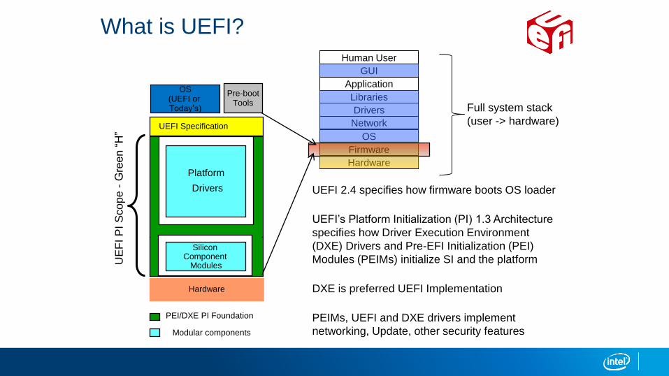
What is UEFI?
UEFI 2.4 specifies how firmware boots OS loader
UEFI’s Platform Initialization (PI) 1.3 Architecture
specifies how Driver Execution Environment
(DXE) Drivers and Pre-EFI Initialization (PEI)
Modules (PEIMs) initialize SI and the platform
DXE is preferred UEFI Implementation
PEIMs, UEFI and DXE drivers implement
networking, Update, other security features
Hardware
OS(UEFI or Today’s)
Pre-bootTools
UEFI Specification
Silicon Component
Modules
Platform
Drivers
UE
FI
PI
Sco
pe
-G
ree
n “
H”
PEI/DXE PI Foundation
Modular components
Network
Hardware
Firmware
OS
Drivers
Libraries
Application
GUI
Human User
Full system stack
(user -> hardware)

What’s in UEFI
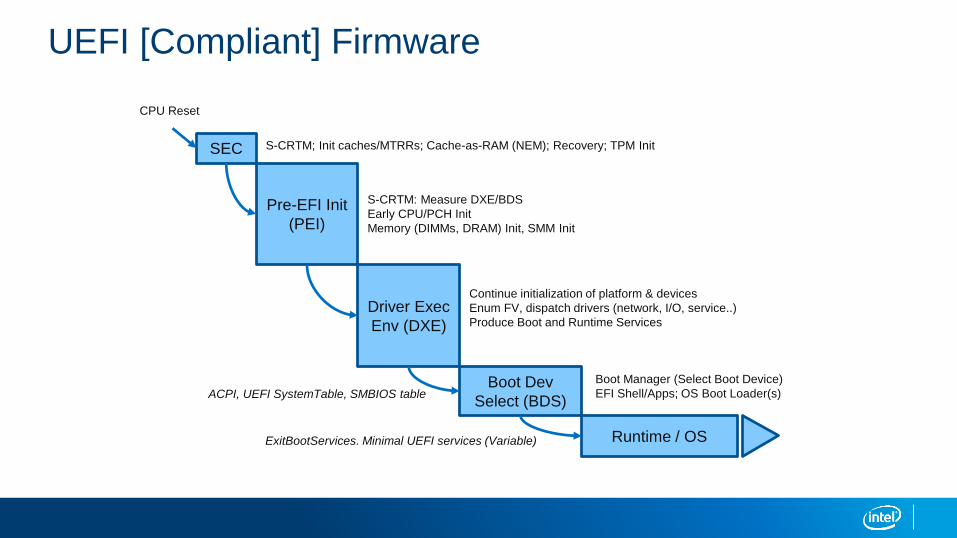
UEFI [Compliant] Firmware
SEC
Pre-EFI Init
(PEI)
Driver Exec
Env (DXE)
Boot Dev
Select (BDS)
Runtime / OS
S-CRTM; Init caches/MTRRs; Cache-as-RAM (NEM); Recovery; TPM Init
S-CRTM: Measure DXE/BDS
Early CPU/PCH Init
Memory (DIMMs, DRAM) Init, SMM Init
Continue initialization of platform & devices
Enum FV, dispatch drivers (network, I/O, service..)
Produce Boot and Runtime Services
Boot Manager (Select Boot Device)
EFI Shell/Apps; OS Boot Loader(s)
ExitBootServices. Minimal UEFI services (Variable)
ACPI, UEFI SystemTable, SMBIOS table
CPU Reset

No one expects the BIOS Inquisition!!

The hole is also greater… than expected…
• 37 unique publicly disclosed issues in the last ~2 years (by only a handful of
researchers)
• Multiple of these are really classes of issues with many instances in
affected firmware products (SMI input pointers, SMI “call-outs”, insecure use
of UEFI variables, etc.)
• Many issues affect multiple vendors at once (S3 boot script, BIOS write
protections, UEFI variables, SMI call-outs, SMI input pointers)
• Issues may need to be checked separately in every product
• And updating firmware is not easy
9
10
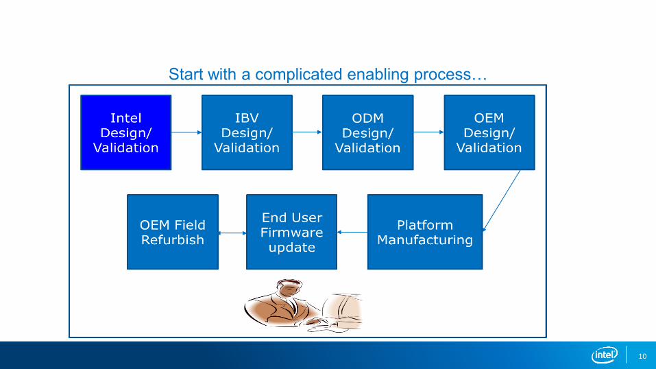
Start with a complicated enabling process…
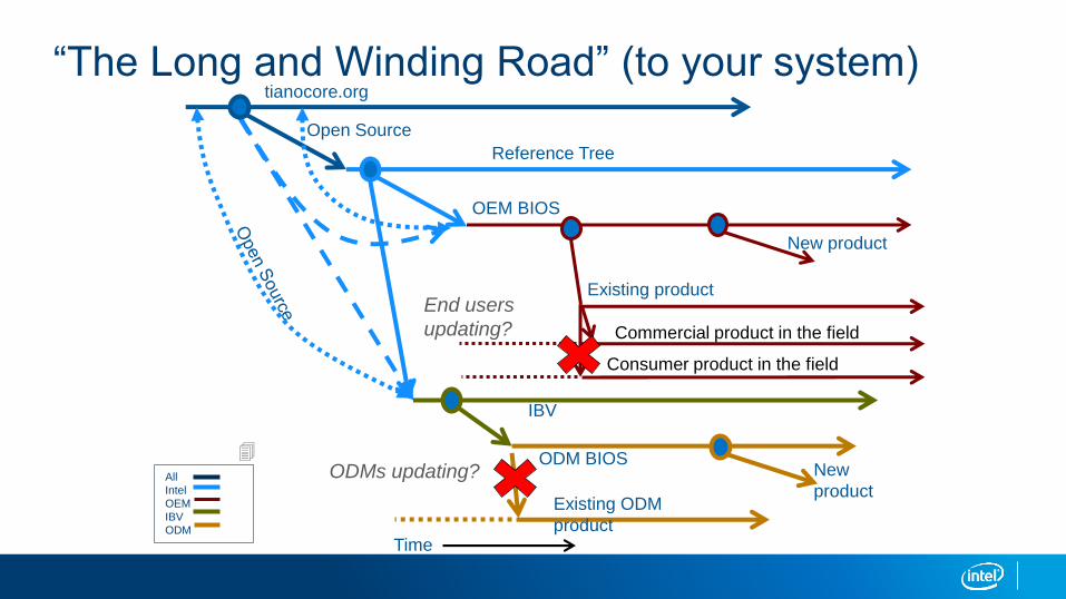
“The Long and Winding Road” (to your system)
Reference Tree
tianocore.org
OEM BIOS
New product
IBV
Existing product
ODM BIOSNew
productExisting ODM
product
Commercial product in the field
Consumer product in the field
End users
updating?
ODMs updating?
Time
Open Source
All
Intel
OEM
IBV
ODM

Some (quick) Examples
1. S3 Boot Script (Sleep/Resume) Issues
2. SMI Handler Call-Outs
3. Bad Pointer Input SMI Vulnerabilities
12
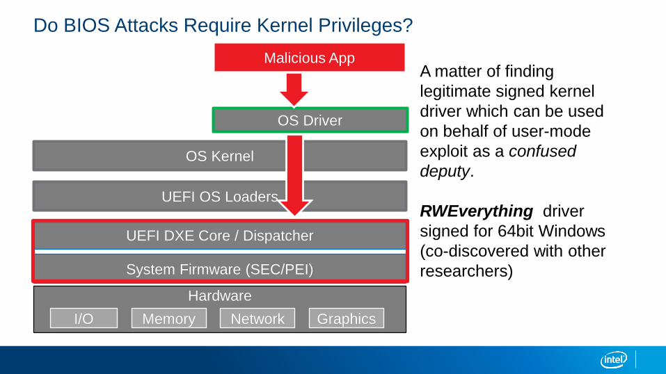
Do BIOS Attacks Require Kernel Privileges?
Hardware
I/O Memory Network Graphics
UEFI DXE Core / Dispatcher
UEFI OS Loaders
System Firmware (SEC/PEI)
OS Kernel
OS Driver
Malicious AppA matter of finding
legitimate signed kernel
driver which can be used
on behalf of user-mode
exploit as a confused
deputy.
RWEverything driver
signed for 64bit Windows
(co-discovered with other
researchers)

A quick summary of many ongoing efforts to improve system firmware security…
14

Parts to Consider…
Finding Issues
– Vulnerability Research
– Security Development Lifecycle activities
– Testing (CHIPSEC and more…)
Hardening
– Development processes and practices
– Threat Model and Mitigations
Community & Ecosystem Engagement
– UEFI Security Response Team
– Intel and Tianocore Advisories
15

16

Intel is looking for (and finding) issues…
2013
Secure Boot Bypass Research (BH 2013)
2014
Tianocore issues (see http://tianocore.org/security)
Multiple Secure Boot Bypasses (independent discovery by other researchers, co-presented at CanSecWest 2014)
Summary of BIOS Attacks (DEFCON 22, Ekoparty 10, Ruxcon 2014)
S3 Boot Script Vulnerabilities (independent discovery by external researchers, presented by Intel at Recon 2015)
2015
SMM Bad Pointer Input Vulnerabilities (CanSecWest 2015)
LTE Modem Security (DEFCON 23)
Attacking VMMs through Firmware (BH 2015)
17

CHIPSEC
Raising the Bar for Platform Security
*Other names and brands may be claimed as the property of others.
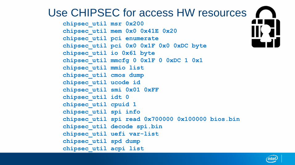
Use CHIPSEC for access HW resourceschipsec_util msr 0x200
chipsec_util mem 0x0 0x41E 0x20
chipsec_util pci enumerate
chipsec_util pci 0x0 0x1F 0x0 0xDC byte
chipsec_util io 0x61 byte
chipsec_util mmcfg 0 0x1F 0 0xDC 1 0x1
chipsec_util mmio list
chipsec_util cmos dump
chipsec_util ucode id
chipsec_util smi 0x01 0xFF
chipsec_util idt 0
chipsec_util cpuid 1
chipsec_util spi info
chipsec_util spi read 0x700000 0x100000 bios.bin
chipsec_util decode spi.bin
chipsec_util uefi var-list
chipsec_util spd dump
chipsec_util acpi list

Known Threats and CHIPSEC modulesChipsec Module PublicationModules/common/ bios_ts.py “BIOS Boot Hijacking and VMware Vulnerabilities Digging” - Sun Bing
Modules/common/ bios_kbrd_buffer.py DEFCON 16: “Bypassing Pre-boot Authentication Passwords by Instrumenting the BIOS
Keyboard Buffer” – Jonathan Brossard
Modules/common/bios_smi.py “Setup for Failure: Defeating SecureBoot” – Corey Kallenberg, Xeno Kovah, John Butterworth,
Sam Cornwell
Modules/remap Preventing & Detecting Xen Hypervisor Subversions – Joanna Rutkowska & Rafal Wojtczuk
Modules/smm_dma Programmed I/O accesses: a threat to Virtual Machine Monitors? – Lioc Duflot & Laurent Absil
Modules/common/ bios_wp.py Black Hat USA 2013 “BIOS Security” – MITRE (Kovah, Butterworth, Kallenberg)
NoSuchCon 2013 “BIOS Chronomancy: Fixing the Static Root of Trust for Measurement” –
MITRE (Kovah, Butterworth, Kallenberg)
Modules/common/ smm.py CanSecWest 2006 “Security Issues Related to Pentium System Management Mode” – Duflot
Modules/common/spi_desc.py Parsing of SPI descriptor access permissions is implemented in “ich_descriptors_tool” which is
part of open source flashrom.
Modules/common/ smrr.py “Attacking SMM Memory via Intel CPU Cache Poisoning” – ITL (Rutkowska, Wojtczuk)
“Getting into the SMRAM: SMM Reloaded” – Duflot, Levillain, Morin, Grumelard
Modules/common/ spi_lock.py FLOCKDN is in flashrom and MITRE's Copernicus
Modules/common/secureboot/keys.py UEFI 2.4 spec Section 28
Modules/common/secureboot/variables.py UEFI 2.4 spec Section 28
Modules/common/uefi/access_uefispec.py UEFI spec – Table 11 “Global Variables”
Modules/tools/smm/smm_ptr.py “A New Class of Vulnerability in SMI Handlers of BIOS/UEFI Firmware” Intel ATR

Some (quick) Examples
Check BIOS Write Protection
S3 Boot Script (Sleep/Resume) Issues
Bad Pointer Input SMI Vulnerabilities
22
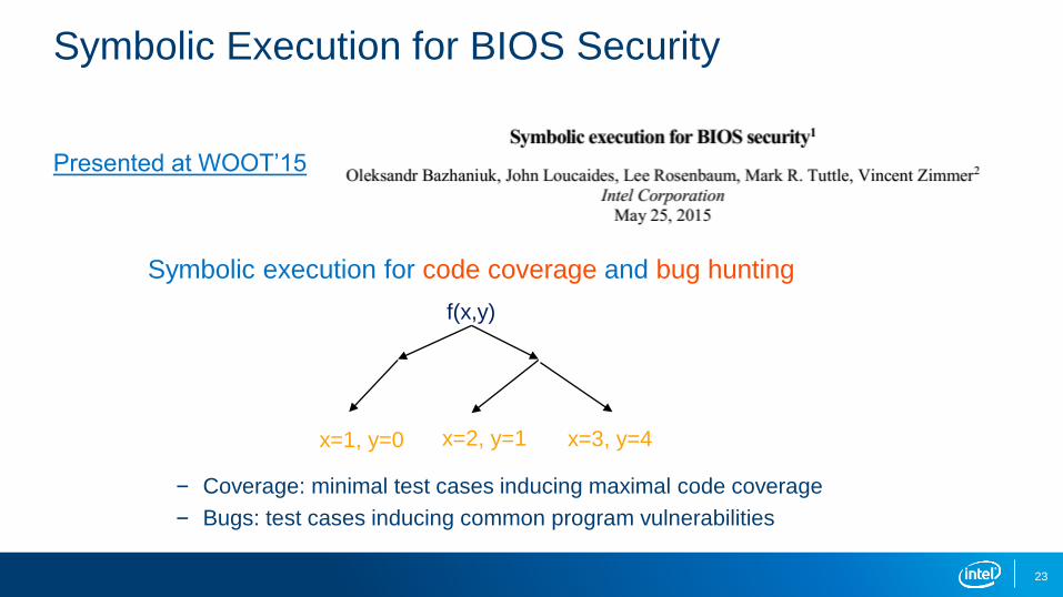
Symbolic Execution for BIOS Security
Presented at WOOT’15
23
Symbolic execution for code coverage and bug hunting
– Coverage: minimal test cases inducing maximal code coverage
– Bugs: test cases inducing common program vulnerabilities
f(x,y)
x=1, y=0 x=2, y=1 x=3, y=4
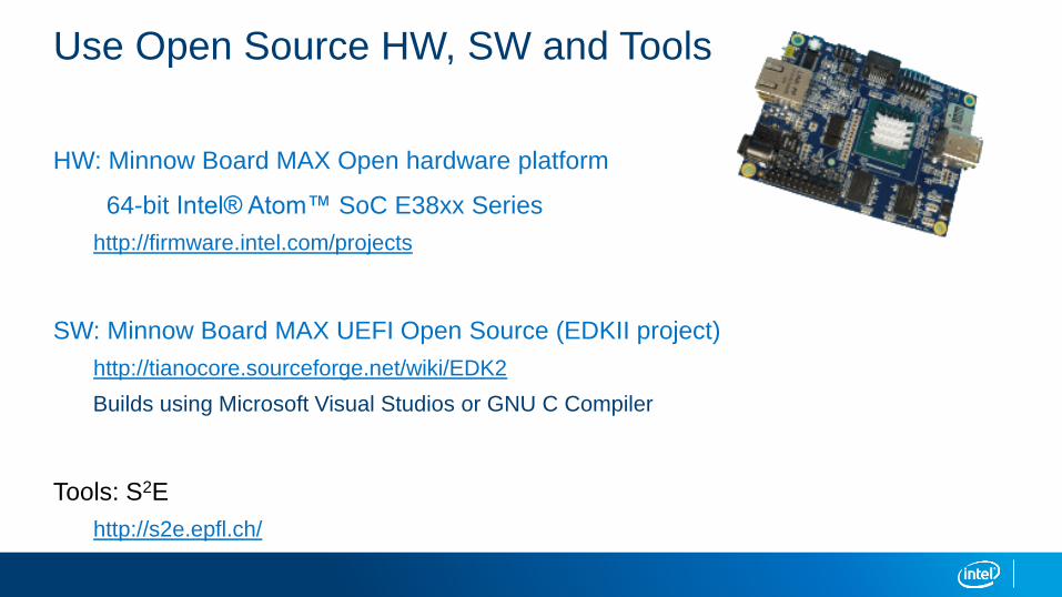
Use Open Source HW, SW and Tools
HW: Minnow Board MAX Open hardware platform
64-bit Intel® Atom™ SoC E38xx Series
http://firmware.intel.com/projects
SW: Minnow Board MAX UEFI Open Source (EDKII project)
http://tianocore.sourceforge.net/wiki/EDK2
Builds using Microsoft Visual Studios or GNU C Compiler
Tools: S2E
http://s2e.epfl.ch/
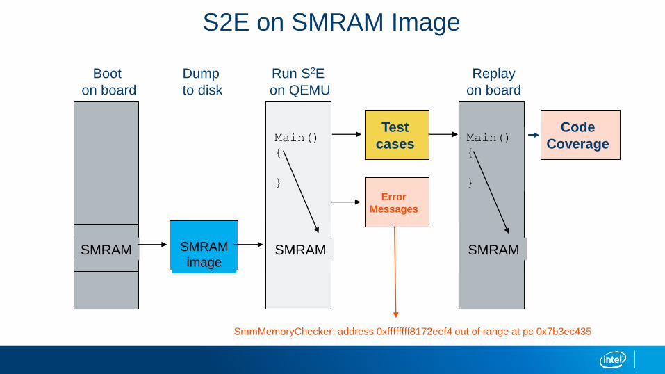
S2E on SMRAM Image
SMRAM SMRAM
image
Boot
on board
Dump
to disk
Run S2E
on QEMU
SMRAM
Main()
{
}
Replay
on board
SMRAM
Main()
{
}
Test
cases
Error
Messages
Code
Coverage
SmmMemoryChecker: address 0xffffffff8172eef4 out of range at pc 0x7b3ec435

26

Development Process
27
Architecture
• Threat Model
• Security Assets, Threats, Objectives, and Requirements
Design
• Design Reviews
Implementation
• Code Review
• Static Analysis
• Test Plan
Deployment
• Survivability Plan
• Incident Response
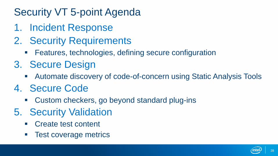
Security VT 5-point Agenda
1. Incident Response
2. Security Requirements Features, technologies, defining secure configuration
3. Secure Design Automate discovery of code-of-concern using Static Analysis Tools
4. Secure Code Custom checkers, go beyond standard plug-ins
5. Security Validation Create test content
Test coverage metrics
28

Know Your Deliverable
29

• Static Analysis into Continuous Integration
• Add Custom Checkers
• Make static analysis do secure design analysis
• Doxygen tags
~~~
• Stay away from project management
– just feed the issues
– impact projects metrics
• Define phases of quality goals
• Define security issues closure as milestone exit criteria
30
Twist the Tools, Sync with Process

31
Hardware Security Testability Interface
Initially…
• Mechanism to help avoid misconfiguration of Security Features
• Provide greater assurance of the Security configuration on all deployed
platforms - Even after configuration changes by IT and/or end-users
• Programmatic method for an Operating System to query security
configuration
Eventually…
• Establish trust between platform, the Intel-provided test module, and the
result published for the Operating System
32
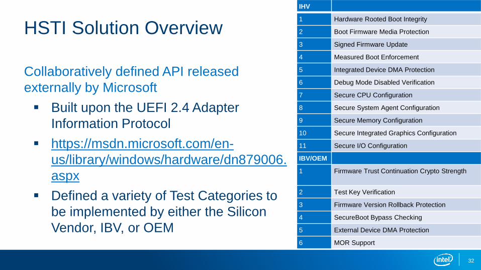
HSTI Solution Overview
Collaboratively defined API released
externally by Microsoft
Built upon the UEFI 2.4 Adapter
Information Protocol
https://msdn.microsoft.com/en-
us/library/windows/hardware/dn879006.
aspx
Defined a variety of Test Categories to
be implemented by either the Silicon
Vendor, IBV, or OEM
IHV
1 Hardware Rooted Boot Integrity
2 Boot Firmware Media Protection
3 Signed Firmware Update
4 Measured Boot Enforcement
5 Integrated Device DMA Protection
6 Debug Mode Disabled Verification
7 Secure CPU Configuration
8 Secure System Agent Configuration
9 Secure Memory Configuration
10 Secure Integrated Graphics Configuration
11 Secure I/O Configuration
IBV/OEM
1 Firmware Trust Continuation Crypto Strength
2 Test Key Verification
3 Firmware Version Rollback Protection
4 SecureBoot Bypass Checking
5 External Device DMA Protection
6 MOR Support
33
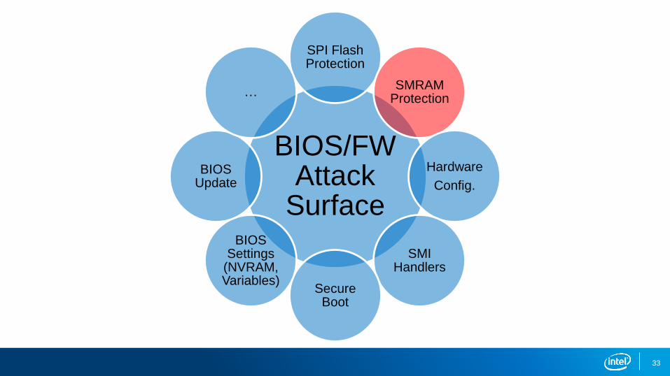
BIOS/FW Attack
Surface
SPI Flash Protection
SMRAM Protection
Hardware
Config.
SMI Handlers
Secure Boot
BIOS Settings
(NVRAM, Variables)
BIOS Update
…

DMA Protection
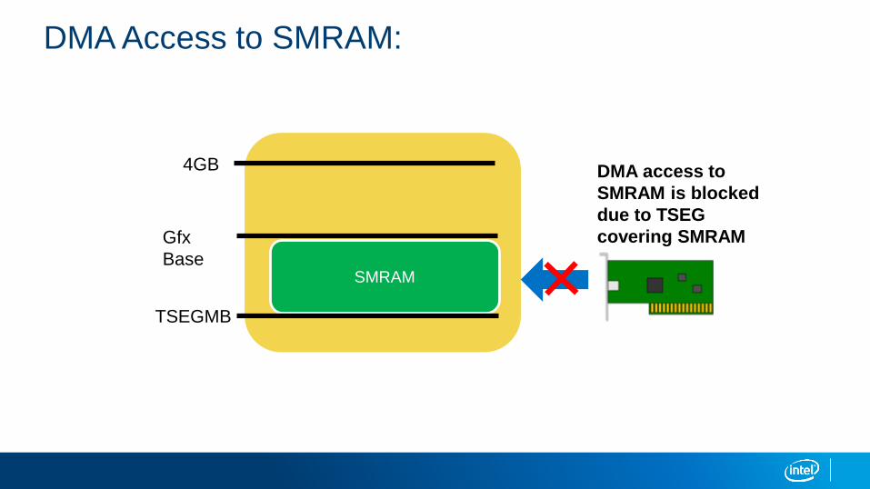
• SMRAM has to be protected from DMA Attack
• Protection from inbound DMA access is guaranteed by programming TSEG range
• When BIOS doesn’t lock down TSEG range configuration, malware can move TSEG outside of where actual SMRAM is
• Then program one of DMA capable devices (e.g. GPU device) or Graphics Aperture to access SMRAM
• Programmed I/O accesses: a threat to Virtual Machine Monitors?
• System Management Mode Design and Security Issues
• BIOS has to lock down configuration required to define range protecting SMRAM from inbound DMA access (e.g. TSEG range)
•chipsec_main --module smm_dma
DMA/GFx Aperture Attacks Against SMRAM
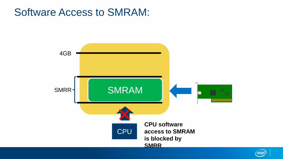
Software Access to SMRAM:
4GB
SMRAM
CPU software
access to SMRAM
is blocked by
SMRR
SMRR
CPU
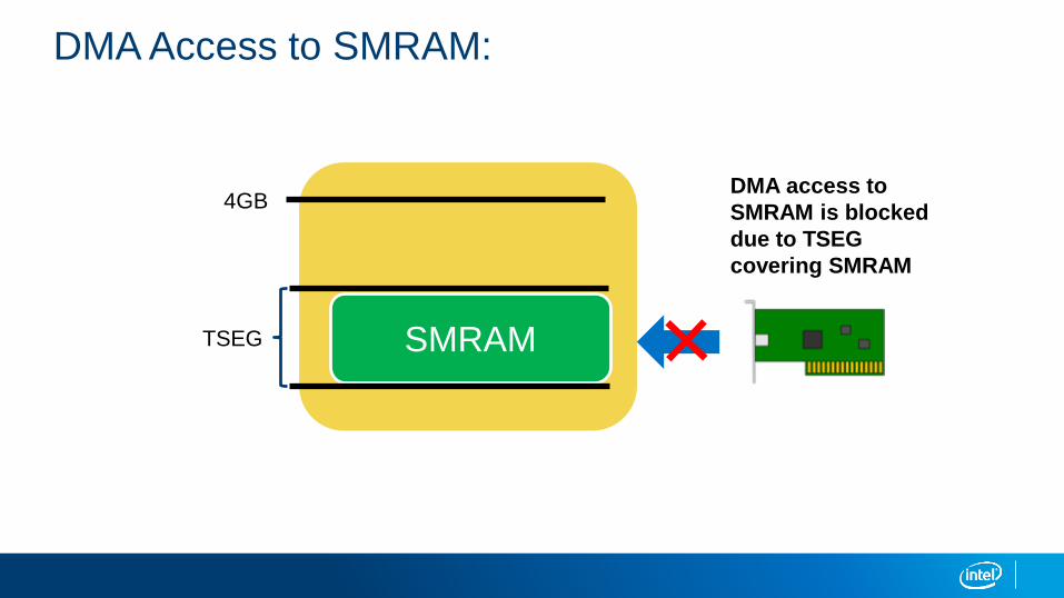
DMA Access to SMRAM:
4GB
SMRAM
DMA access to
SMRAM is blocked
due to TSEG
covering SMRAM
TSEG
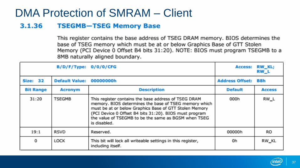
DMA Protection of SMRAM – Client
37
DMA Access to SMRAM:
4GB
SMRAM
DMA access to
SMRAM is blocked
due to TSEG
covering SMRAM
TSEGMB
Gfx
Base

Servers are People (computers) too
Architectural differences
Memory
Multi-processor
Register implementation differences
Feature support differences
Mitigation differences
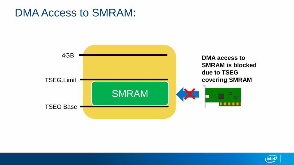
DMA Access to SMRAM:
4GB
SMRAM
DMA access to
SMRAM is blocked
due to TSEG
covering SMRAM
TSEG Base
TSEG.Limit

DMA Protection of SMRAM – Server
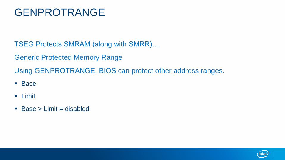
GENPROTRANGE
TSEG Protects SMRAM (along with SMRR)…
Generic Protected Memory Range
Using GENPROTRANGE, BIOS can protect other address ranges.
Base
Limit
Base > Limit = disabled

GENPROTRANGE Base and Limit

DMA Access to SMRAM:
Genprotrange[1].Base
Genprotrange[1].Limit
Genprotrange[0].Base
Genprotrange[0].Limit

After all, we’re in this together…
45

Response Process
1. Issue Discovery
[email protected] [email protected] (other security teams)
2. Investigation and Disposition of Impacts
PSIRT BIOS Core, representing BIOS leads in every segment
3. Mitigation Development and Validation
4. Non-public Communication for Mitigation Development/Deployment
Technical Advisories
USRT Coordination (http://uefi.org/security)
5. Public Communication
https://security-center.intel.com
http://tianocore.org/security
46

CHIPSEC Information
On the web: https://github.com/chipsec/chipsec
Email List: https://lists.01.org/mailman/listinfo/chipsec
Gaining activity/support from community
External interest in
– Deployable drivers
– Supporting other platforms/architectures
– Greater coverage of issues
– Increased user-friendliness
Contact: [email protected]
47

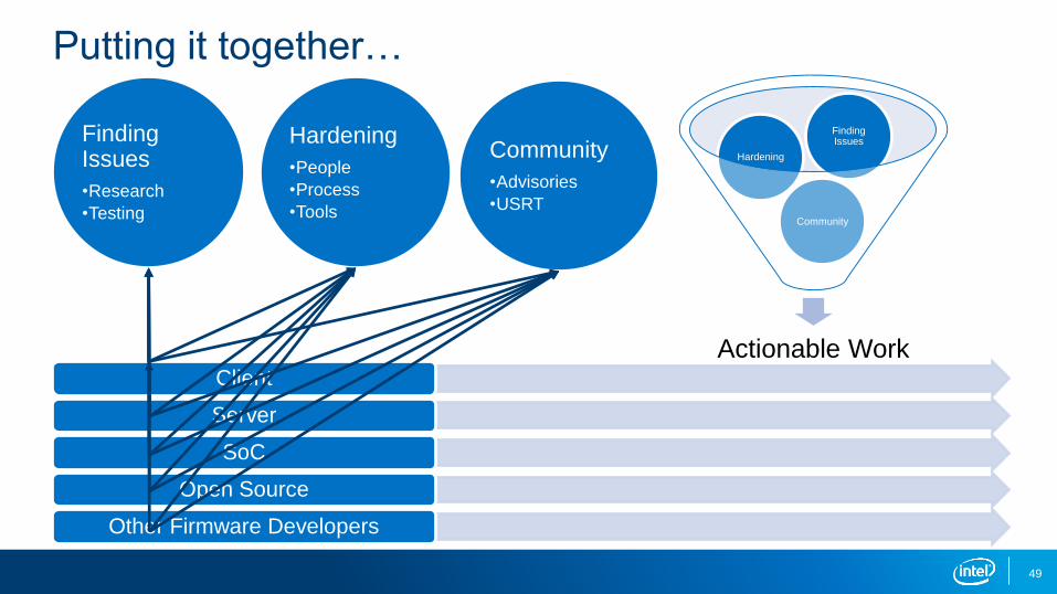
Putting it together…
Client
Server
SoC
Open Source
Other Firmware Developers
48
Actionable Work
Community
Hardening
Finding IssuesFinding
Issues
•Research
•Testing
Hardening
•People
•Process
•Tools
Community
•Advisories
•USRT
Putting it together…
Client
Server
SoC
Open Source
Other Firmware Developers
49
Actionable Work
Community
Hardening
Finding IssuesFinding
Issues
•Research
•Testing
Hardening
•People
•Process
•Tools
Community
•Advisories
•USRT
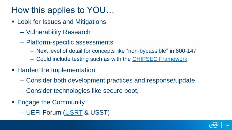
How this applies to YOU…
Look for Issues and Mitigations
– Vulnerability Research
– Platform-specific assessments
– Next level of detail for concepts like “non-bypassible” in 800-147
– Could include testing such as with the CHIPSEC Framework
Harden the Implementation
– Consider both development practices and response/update
– Consider technologies like secure boot,
Engage the Community
– UEFI Forum (USRT & USST)
50

Please visit Intel in the Show Floor Area in Booth 100

Example 1
52
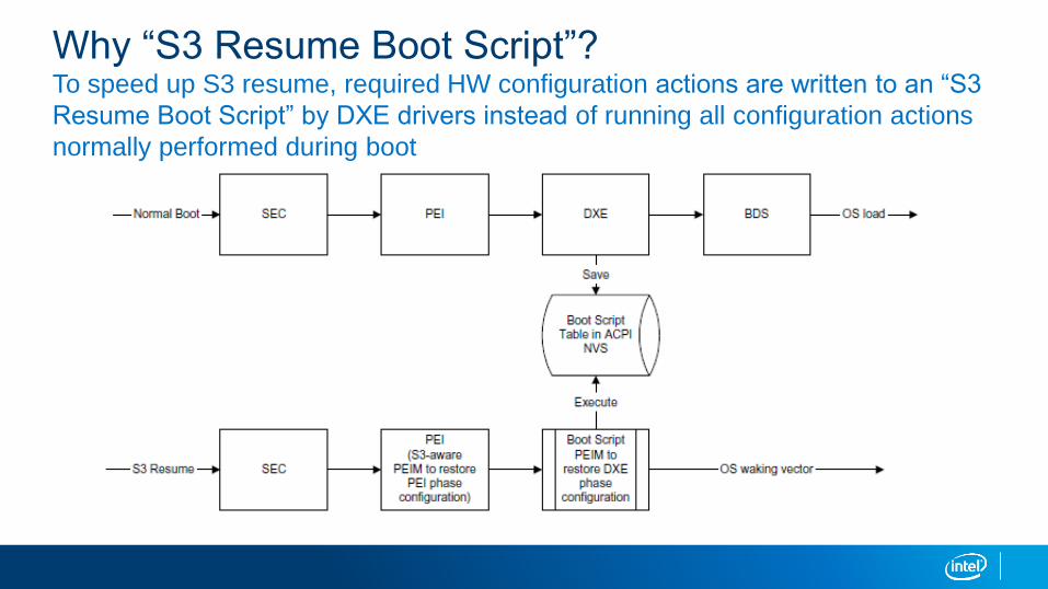
Why “S3 Resume Boot Script”?To speed up S3 resume, required HW configuration actions are written to an “S3
Resume Boot Script” by DXE drivers instead of running all configuration actions
normally performed during boot
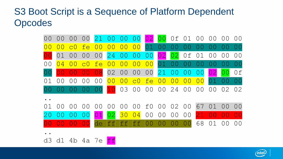
S3 Boot Script is a Sequence of Platform Dependent
Opcodes
00 00 00 00 21 00 00 00 02 00 0f 01 00 00 00 00
00 00 c0 fe 00 00 00 00 01 00 00 00 00 00 00 00
00 01 00 00 00 24 00 00 00 02 02 0f 01 00 00 00
00 04 00 c0 fe 00 00 00 00 01 00 00 00 00 00 00
00 00 00 00 08 02 00 00 00 21 00 00 00 02 00 0f
01 00 00 00 00 00 00 c0 fe 00 00 00 00 01 00 00
00 00 00 00 00 10 03 00 00 00 24 00 00 00 02 02
..
01 00 00 00 00 00 00 00 f0 00 02 00 67 01 00 00
20 00 00 00 01 02 30 04 00 00 00 00 21 00 00 00
00 00 00 00 de ff ff ff 00 00 00 00 68 01 00 00
..
d3 d1 4b 4a 7e ff

Decoding Opcodes
# chipsec_util.py uefi s3bootscript
[000] Entry at offset 0x0000 (length = 0x21):
Data:
02 00 0f 01 00 00 00 00 00 00 c0 fe 00 00 00 00
01 00 00 00 00 00 00 00 00
Decoded:
Opcode : S3_BOOTSCRIPT_MEM_WRITE (0x02)
Width : 0x00 (1 bytes)
Address: 0xFEC00000
Count : 0x1
Values : 0x00
..
[359] Entry at offset 0x2F2C (length = 0x20):
Data:
01 02 30 04 00 00 00 00 21 00 00 00 00 00 00 00
de ff ff ff 00 00 00 00
Decoded:
Opcode : S3_BOOTSCRIPT_IO_READ_WRITE (0x01)
Width : 0x02 (4 bytes)
Address: 0x00000430
Value : 0x00000021
Mask : 0xFFFFFFDE
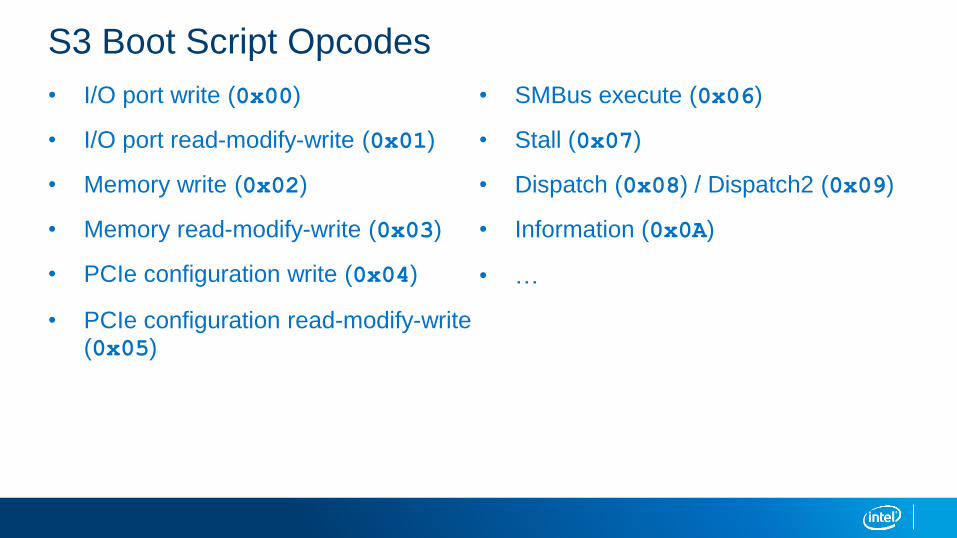
S3 Boot Script Opcodes
• I/O port write (0x00)
• I/O port read-modify-write (0x01)
• Memory write (0x02)
• Memory read-modify-write (0x03)
• PCIe configuration write (0x04)
• PCIe configuration read-modify-write (0x05)
• SMBus execute (0x06)
• Stall (0x07)
• Dispatch (0x08) / Dispatch2 (0x09)
• Information (0x0A)
• …
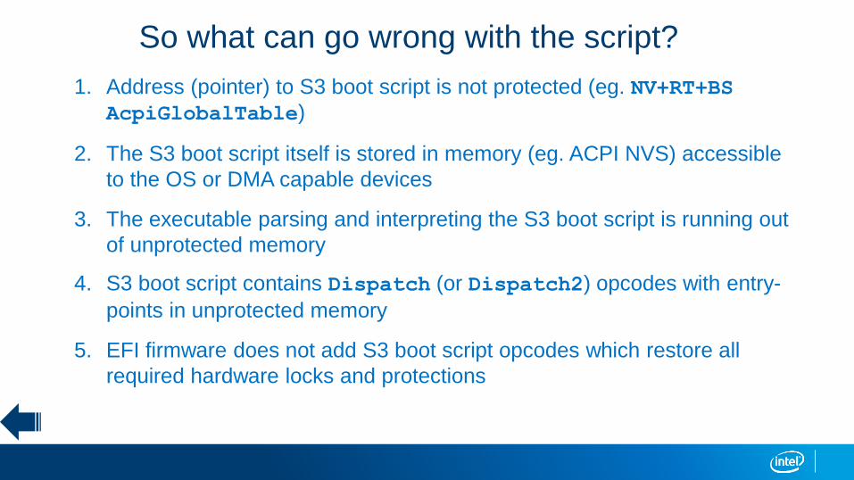
So what can go wrong with the script?
1. Address (pointer) to S3 boot script is not protected (eg. NV+RT+BS
AcpiGlobalTable)
2. The S3 boot script itself is stored in memory (eg. ACPI NVS) accessible
to the OS or DMA capable devices
3. The executable parsing and interpreting the S3 boot script is running out
of unprotected memory
4. S3 boot script contains Dispatch (or Dispatch2) opcodes with entry-
points in unprotected memory
5. EFI firmware does not add S3 boot script opcodes which restore all
required hardware locks and protections
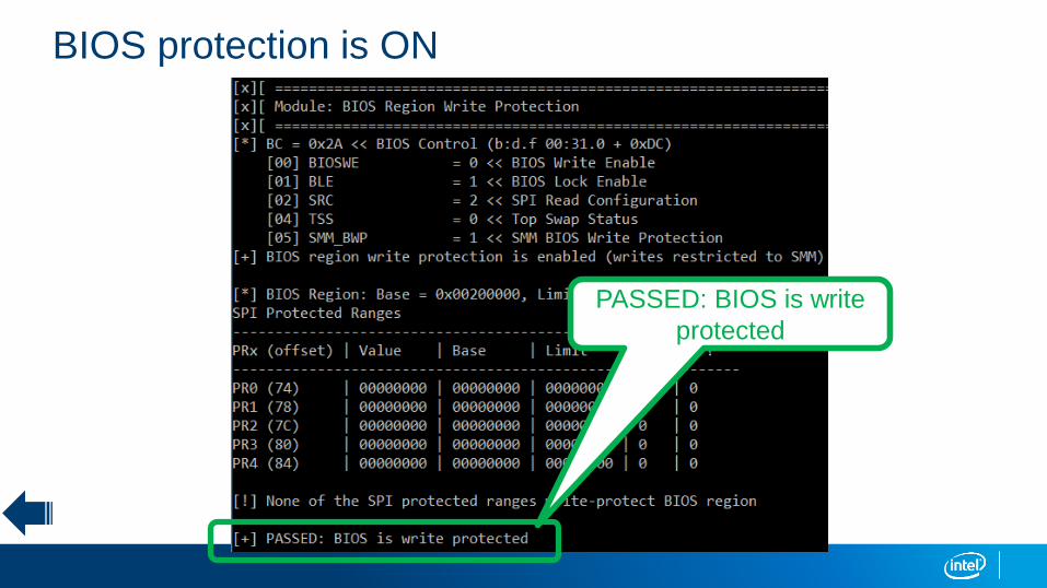
BIOS protection is ON
PASSED: BIOS is write
protected
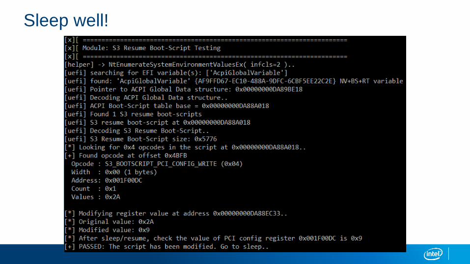
Sleep well!

Oh wait…
FAILED: BIOS is NOT
protected completely
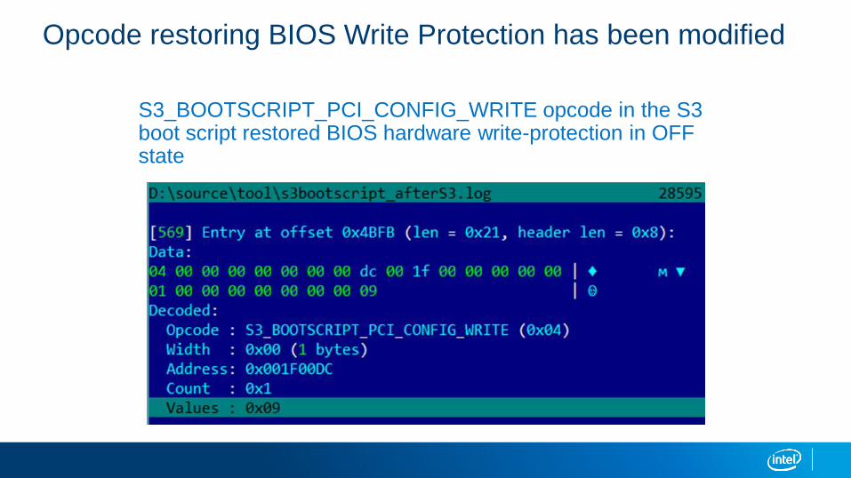
Opcode restoring BIOS Write Protection has been modified
S3_BOOTSCRIPT_PCI_CONFIG_WRITE opcode in the S3 boot script restored BIOS hardware write-protection in OFF state
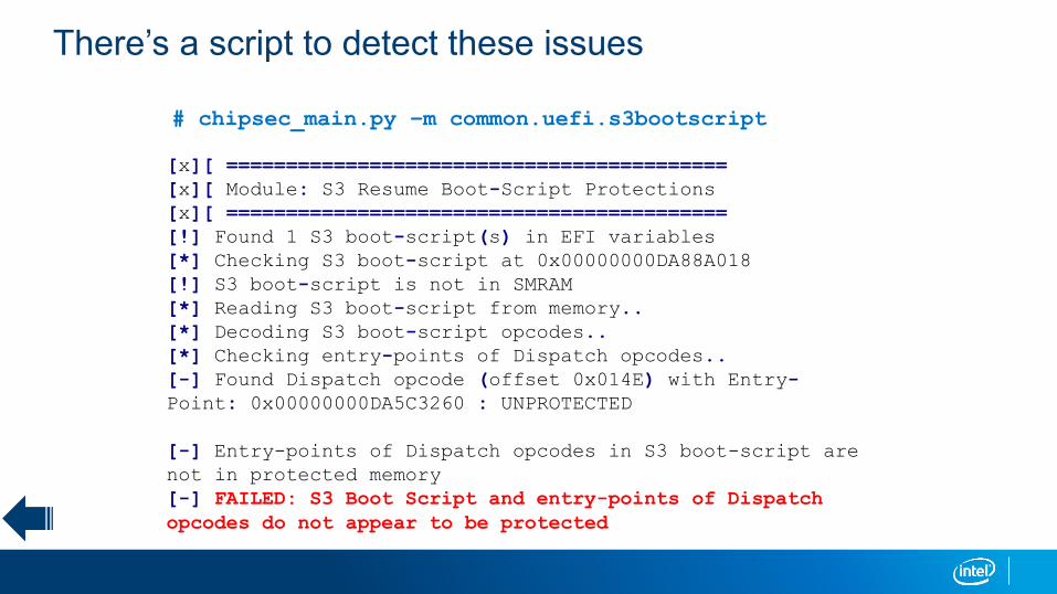
There’s a script to detect these issues
# chipsec_main.py –m common.uefi.s3bootscript
[x][ ==========================================
[x][ Module: S3 Resume Boot-Script Protections
[x][ ==========================================
[!] Found 1 S3 boot-script(s) in EFI variables
[*] Checking S3 boot-script at 0x00000000DA88A018
[!] S3 boot-script is not in SMRAM
[*] Reading S3 boot-script from memory..
[*] Decoding S3 boot-script opcodes..
[*] Checking entry-points of Dispatch opcodes..
[-] Found Dispatch opcode (offset 0x014E) with Entry-
Point: 0x00000000DA5C3260 : UNPROTECTED
[-] Entry-points of Dispatch opcodes in S3 boot-script are
not in protected memory
[-] FAILED: S3 Boot Script and entry-points of Dispatch
opcodes do not appear to be protected

Protecting the S3 Boot Script
1. Do not keep address (pointer) to S3 Boot Script table in unprotected non-volatile UEFI variable (ex. NV+RT+BS AcpiGlobalVariable)
2. Do not keep address (pointer) to S3 Boot Script table or to a structure containing address of the script in unprotected non-volatile UEFI variable (ex. NV+RT+BS AcpiGlobalVariable)
3. Do not save the S3 Boot Script table to memory accessible by the OS or DMA capable devices
4. Do not save the PEI executable that parses and executes the S3 Boot Script table and any other PEI executable(s) needed for S3 resume to memory accessible by the OS or DMA capable devices
5. Saving a pointer to the S3 boot script in a UEFI variable that is accessible by the OS or DMA capable devices
6. Review the S3 Boot Script for Dispatch opcodes and establish whether the target code is protected.

Example 2

Once upon a time…
• In 2009, SMI call-out vulnerabilities were discovered by Rafal Wojtczuk and
Alex Tereshkin in EFI SMI handlers (Attacking Intel BIOS) and by Filip
Wecherowski in legacy SMI (BIOS SMM Privilege Escalation Vulnerabilities)
• Also discussed by Loic Duflot in System Management Mode Design and
Security Issues
• In 2015(!) researchers from LegbaCore found that many modern systems are
still vulnerable to these issues How Many Million BIOS Would You Like To
Infect (paper)
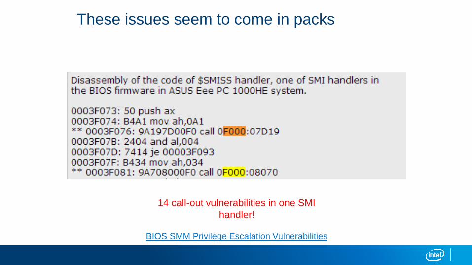
These issues seem to come in packs
14 call-out vulnerabilities in one SMI
handler!
BIOS SMM Privilege Escalation Vulnerabilities

Legacy SMI Handlers Calling Out of SMRAM
Phys Memory
SMRAMCALL F000:8070
Legacy BIOS Shadow
(F/ E-segments)
PA = 0xF0000
1 MB

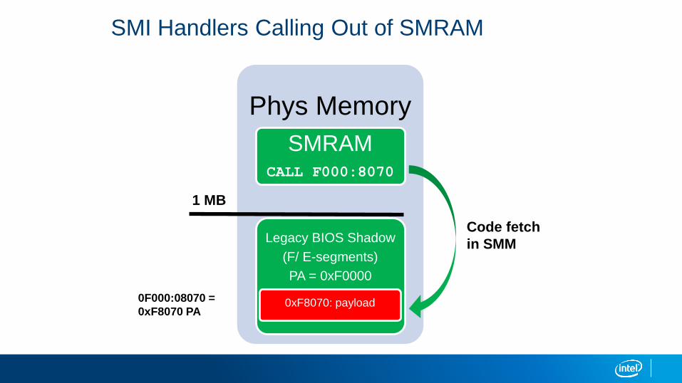
SMI Handlers Calling Out of SMRAM
Phys Memory
SMRAMCALL F000:8070
Legacy BIOS Shadow
(F/ E-segments)
PA = 0xF0000
1 MB
Code fetch
in SMM
SMI Handlers Calling Out of SMRAM
Phys Memory
SMRAMCALL F000:8070
Legacy BIOS Shadow
(F/ E-segments)
PA = 0xF0000
1 MB
0xF8070: payload0F000:08070 =
0xF8070 PA
Code fetch
in SMM

BIOS developers can easily detect call-outs
1. A “simple” HW debugger script to step on branches and verify that target address of the branch is within SMRAM
2. Enable SMM Code Access Check HW feature on pre-production systems based on newer CPUs to weed out all “intended” code fetches outside of SMRAM from SMI drivers
3. NX based soft SMM Code Access Check patches by Phoenix look promising
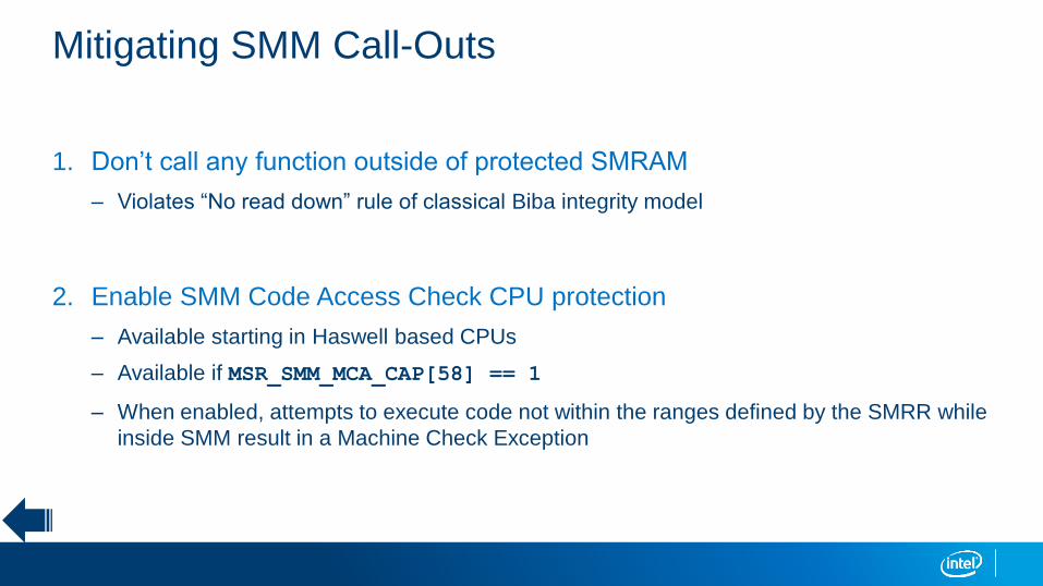
Mitigating SMM Call-Outs
1. Don’t call any function outside of protected SMRAM
– Violates “No read down” rule of classical Biba integrity model
2. Enable SMM Code Access Check CPU protection
– Available starting in Haswell based CPUs
– Available if MSR_SMM_MCA_CAP[58] == 1
– When enabled, attempts to execute code not within the ranges defined by the SMRR while
inside SMM result in a Machine Check Exception

Blocking Code Fetch Outside of SMRAM
Phys Memory
SMRAMCALL F000:8070
Legacy BIOS Shadow
(F/ E-segments)
PA = 0xF0000
1 MB
0xF8070: payload0F000:08070 =
0xF8070 PA
Code fetch
in SMM
causes MC
exception
Example 3

System Management Interrupt (SMI) Handlers
SMRR_PHYSBAS
E
SMRAM
0x00000000
0xFFFFFFFF
SMI
handlers
SMM state
save area
SMBASE + 8000h
SMBASE
SMBASE + FFFFh
SMRAM
SMBASE + FC00h

Pointer Arguments to SMI Handlers
Phys Memory
SMI Handlers in SMRAM
OS Memory
SMI Handler writes result to a buffer at address passed in RBX…
RAX (code)
RBX (pointer)
RCX (function)
RDX
RSI
RDI
SMI handler structure
SMI
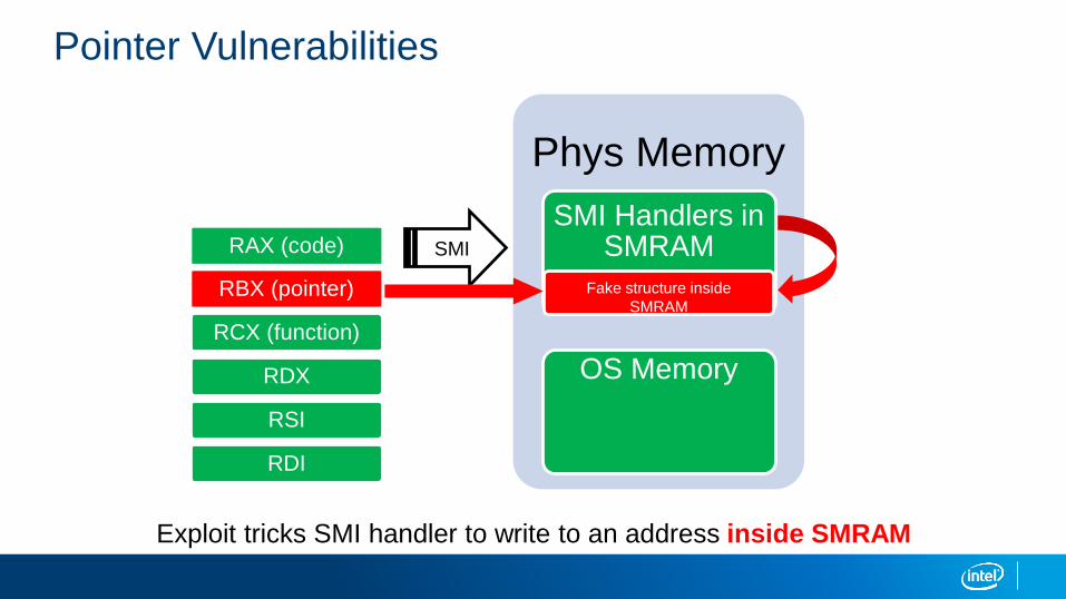
Pointer Vulnerabilities
Phys Memory
SMI Handlers in SMRAM
OS Memory
Exploit tricks SMI handler to write to an address inside SMRAM
RAX (code)
RBX (pointer)
RCX (function)
RDX
RSI
RDI
Fake structure inside
SMRAM
SMI
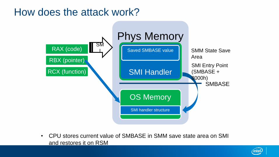
How does the attack work?
Phys Memory
SMI Handler
OS Memory
• CPU stores current value of SMBASE in SMM save state area on SMI
and restores it on RSM
RAX (code)
RBX (pointer)
RCX (function)
SMI handler structure
SM
I
SMBASE
SMM State Save
Area
Saved SMBASE value
SMI Entry Point
(SMBASE +
8000h)
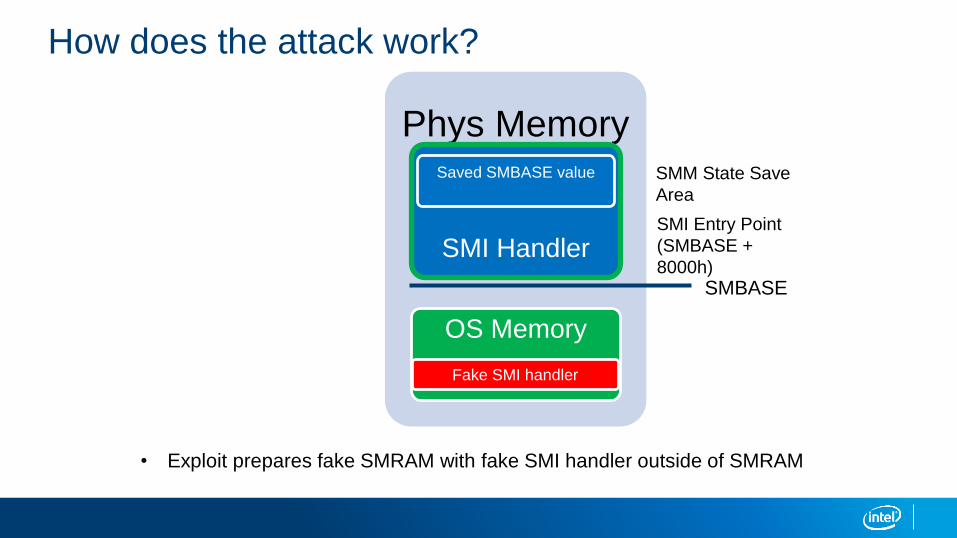
How does the attack work?
Phys Memory
SMI Handler
OS Memory
• Exploit prepares fake SMRAM with fake SMI handler outside of SMRAM
Fake SMI handler
SMBASE
Saved SMBASE value SMM State Save
Area
SMI Entry Point
(SMBASE +
8000h)

How does the attack work?
Phys Memory
SMI Handler
OS Memory
• Exploit triggers SMI w/ RBX pointing to saved SMBASE address in SMRAM
• SMI handler overwrites saved SMBASE on exploit’s behalf with address of fake SMI handler
outside of SMRAM (e.g. 0 PA)
RAX (code)
RBX (pointer)
RCX (function)
SM
I
SMBASE
Fake SMI handler
Saved SMBASE value SMM State Save
Area
SMI Entry Point
(SMBASE +
8000h)

How does the attack work?
Phys Memory
SMI Handler
OS Memory
• Exploit triggers another SMI
• CPU executes fake SMI handler at new entry point outside of original
protected SMRAM because SMBASE location changed
SM
I
SMBASEFake SMI handler
Saved SMBASE value SMM State Save
Area
New SMI Entry Point
How does the attack work?
Phys Memory
SMI Handler(SMRAM is not protected)
OS Memory
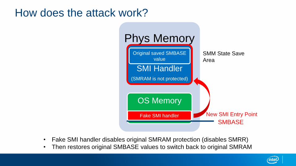
• Fake SMI handler disables original SMRAM protection (disables SMRR)
• Then restores original SMBASE values to switch back to original SMRAM
SMBASEFake SMI handler
Original saved SMBASE
valueSMM State Save
Area
New SMI Entry Point
How does the attack work?
Phys Memory
SMI Handler
(SMRAM is not protected)
OS Memory
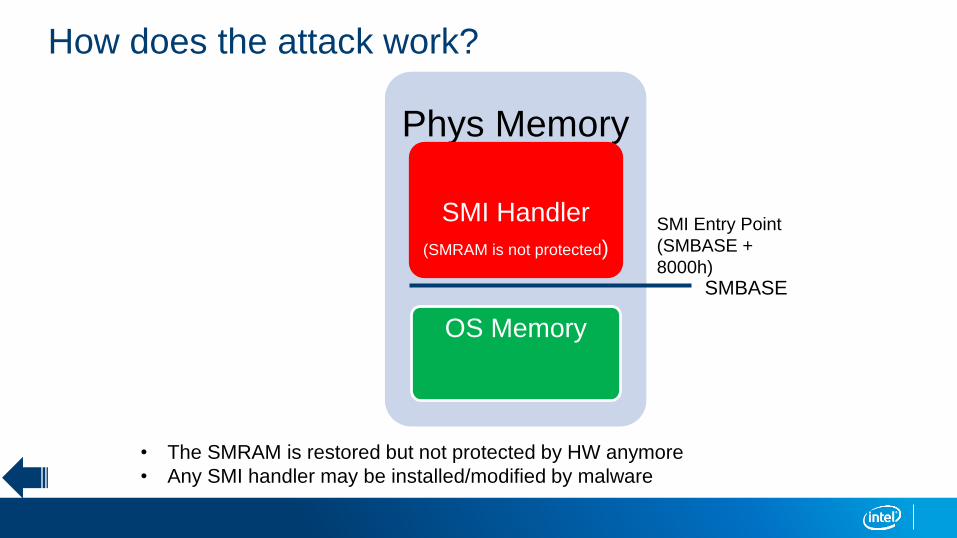
• The SMRAM is restored but not protected by HW anymore
• Any SMI handler may be installed/modified by malware
SMBASE
SMI Entry Point
(SMBASE +
8000h)
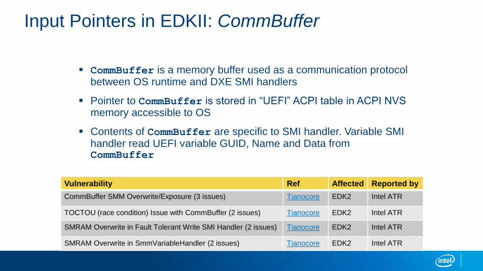
Input Pointers in EDKII: CommBuffer
CommBuffer is a memory buffer used as a communication protocol between OS runtime and DXE SMI handlers
Pointer to CommBuffer is stored in “UEFI” ACPI table in ACPI NVS memory accessible to OS
Contents of CommBuffer are specific to SMI handler. Variable SMI handler read UEFI variable GUID, Name and Data from CommBuffer
Vulnerability Ref Affected Reported by
CommBuffer SMM Overwrite/Exposure (3 issues) Tianocore EDK2 Intel ATR
TOCTOU (race condition) Issue with CommBuffer (2 issues) Tianocore EDK2 Intel ATR
SMRAM Overwrite in Fault Tolerant Write SMI Handler (2 issues) Tianocore EDK2 Intel ATR
SMRAM Overwrite in SmmVariableHandler (2 issues) Tianocore EDK2 Intel ATR

Attacking CommBuffer Pointer
SecurityPkg/VariableAuthenticated/RuntimeDxe:
SmmVariableHandler (
...
SmmVariableFunctionHeader = (SMM_VARIABLE_COMMUNICATE_HEADER *)CommBuffer;
switch (SmmVariableFunctionHeader->Function) {
case SMM_VARIABLE_FUNCTION_GET_VARIABLE:
SmmVariableHeader = (SMM_VARIABLE_COMMUNICATE_ACCESS_VARIABLE *)
SmmVariableFunctionHeader->Data;
Status = VariableServiceGetVariable (
...
(UINT8 *)SmmVariableHeader->Name + SmmVariableHeader->NameSize
);
VariableServiceGetVariable (
...
OUT VOID *Data
)
...
CopyMem (Data, GetVariableDataPtr (Variable.CurrPtr), VarDataSize);
SMRAMCommBuffer

Mitigating CommBuffer Attack
SMI Handlers often have multiple commands, calling a different function for each command and take command specific arguments
Note the calls to SmmIsBufferOutsideSmmValid. This checks for addresses to overlap with SMRAM range
SmiHandler() {
// check CommBuffer is outside SMRAM
if (!SmmIsBufferOutsideSmmValid(CommBuffer, Size)) {
return EFI_SUCCESS;
}
switch(command)
case 1: do_command1(CommBuffer);
case 2: do_command2(CommBuffer);
…SMRAMCommBuffer
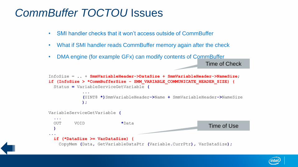
CommBuffer TOCTOU Issues
• SMI handler checks that it won’t access outside of CommBuffer
• What if SMI handler reads CommBuffer memory again after the check
• DMA engine (for example GFx) can modify contents of CommBuffer
InfoSize = .. + SmmVariableHeader->DataSize + SmmVariableHeader->NameSize;
if (InfoSize > *CommBufferSize - SMM_VARIABLE_COMMUNICATE_HEADER_SIZE) {
Status = VariableServiceGetVariable (
...
(UINT8 *)SmmVariableHeader->Name + SmmVariableHeader->NameSize
);
VariableServiceGetVariable (
...
OUT VOID *Data
)
...
if (*DataSize >= VarDataSize) {
CopyMem (Data, GetVariableDataPtr (Variable.CurrPtr), VarDataSize);
Time of Check
Time of Use

Detecting Bad SMI Input Pointers
1. Allocate a buffer in physical memory
2. Set GP registers to address of allocated memory buffer
3. Invoke SW SMI
4. Check fill pattern
[x][ =======================================================================
[x][ Module: A tool to test SMI handlers for pointer validation vulnerabilies
[x][ =======================================================================
Usage: chipsec_main -m tools.smm.smm_ptr [ -a <fill_byte>,<size>,<config_file>,<address> ]
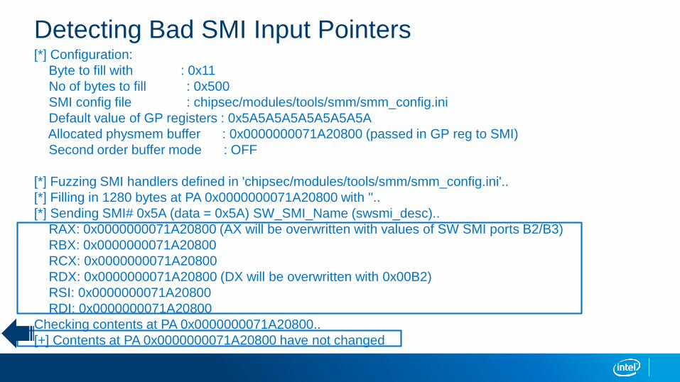
Detecting Bad SMI Input Pointers[*] Configuration:
Byte to fill with : 0x11
No of bytes to fill : 0x500
SMI config file : chipsec/modules/tools/smm/smm_config.ini
Default value of GP registers : 0x5A5A5A5A5A5A5A5A
Allocated physmem buffer : 0x0000000071A20800 (passed in GP reg to SMI)
Second order buffer mode : OFF
[*] Fuzzing SMI handlers defined in 'chipsec/modules/tools/smm/smm_config.ini'..
[*] Filling in 1280 bytes at PA 0x0000000071A20800 with ''..
[*] Sending SMI# 0x5A (data = 0x5A) SW_SMI_Name (swsmi_desc)..
RAX: 0x0000000071A20800 (AX will be overwritten with values of SW SMI ports B2/B3)
RBX: 0x0000000071A20800
RCX: 0x0000000071A20800
RDX: 0x0000000071A20800 (DX will be overwritten with 0x00B2)
RSI: 0x0000000071A20800
RDI: 0x0000000071A20800
Checking contents at PA 0x0000000071A20800..
[+] Contents at PA 0x0000000071A20800 have not changed
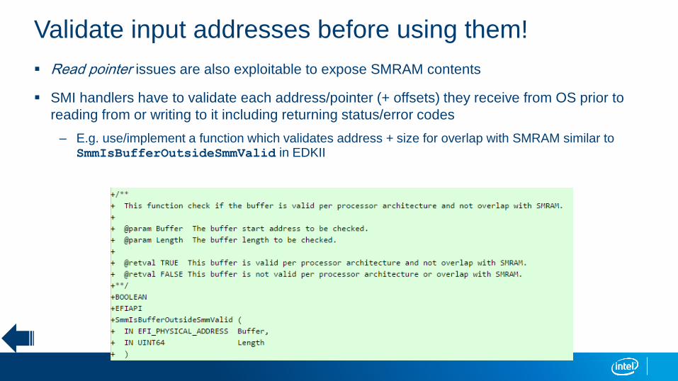
Validate input addresses before using them!
Read pointer issues are also exploitable to expose SMRAM contents
SMI handlers have to validate each address/pointer (+ offsets) they receive from OS prior to
reading from or writing to it including returning status/error codes
– E.g. use/implement a function which validates address + size for overlap with SMRAM similar to SmmIsBufferOutsideSmmValid in EDKII