substrates for large area oled, olec - swissphotonics for large area oled, olec ... additional...
TRANSCRIPT

Substrates for large area OLED, OLEC
Peter Chabrecek, Uriel Sonderegger
New application of SEFAR® fabric
Including results from KTI cooperation projects: WoCoLED Project no. 12055.1 PFNM-NM WoWLED Project no 13466.1 PFFLE-NM

Sefar AG
World leading manufacturer of monofilament precision fabrics for : filter components & screen printing others applications (architecture, medicine, etc.)
Annual sales of about 300 million CHF and 2000 employees worldwide Two headquarters in Switzerland: Thal and Heiden
Corporate headquarters in Thal (SG) Operational headquarters in Heiden (AR)
Substrates for large area OLED, OLEC
Large area SSL, 30.10.2014

New application of SEFAR® fabric
As a part of transparent flexible electrode (substrate) in optoelectronic industry (as replacement of ITO coated foils)
The fabric has following properties:
- highly transparent and very conductive
- more flexible and mechanically stabile than foils, larger surface areas
- allowing preparation of shaped (fabrics reinforced) objects
- allowing R-2-R manufacturing process in industrial scale
Substrates for large area OLED, OLEC
The electrodes, produced at Sefar from these conductive transparent fabrics, are already used in production of electroluminescent devices or flexible DSC.
Large area SSL, 30.10.2014

• Indium tin oxide (ITO) is the incumbent market solution today, but:
1. The uncertainty associated with the cost of raw indium is forcing many users to consider alternatives.
2. The limited sheet resistance (50-350 ohm/sqr) will also not readily meet the needs of emerging applications.
3. ITO-on-PET offers limited flexibility, but it does not survive when bent too much and/or too many times.
4. These drawbacks open space for ITO alternatives.
• ITO alternatives include: • Silver nanowires • Carbon nanotubes • Graphene • PEDOT • Metal mesh
No single technology fits for all solution satisfying all the emerging needs.
Substrates for large area OLED, OLEC
Large area SSL, 30.10.2014

ITO alternatives:
1. Graphene is a late entrant onto the scene and is currently over-priced and under-performing. It is however a technology that receives considerable attention due to its mechanical property and solution deposition.
2. Silver nanowire is a commercially well-funded solution and has already demonstrated initial product acceptance from a variety of end users. However, stability against corrosion is still a big problem as well as a price.
3. Carbon nanotubes offer a mederate sheet resistance and transparency but promise to minimize stack layers.
4. PEDOT has come a long way in terms of sheet resistance but is today only on a par with existing ITO-on-PET solutions.
5. Metal mesh offers low sheet resistance, low cost and the potential to skip the patterning step. There are multiple ways of manufacturing metal. In many instances, however, yield is still a sticky question mark.
Substrates for large area OLED, OLEC
Large area SSL, 30.10.2014

Sefar electrodes comprised a plastic foil and highly transparent and conductive fabrics embedded in a transparent and stable polymer matrix.
White color represents polymer fibers, black color represents metallic or metalized fibers.
Light blue color represents a polymer coating, gold color represents a transparent foil.
Electrode properties:
- highly transparent (T>87%) and very conductive (R<1 Ω)
- impermeable for liquids and gases
- more flexible and mechanically stabile than foils
- allowing non-expensive roll-to-roll production process
Substrates for large area OLED, OLEC
Large area SSL, 30.10.2014

• The fabrics are made from transparent synthetic fibers (PEN) with precisely defined large openings and metallic wires placed on precisely defined directions with precisely defined distances (gaps).
• Fabrics are coated with very high transparent (cross linked) polymer layers - thickness is controlled in such a way that the substrate is still conductive from one side, but non-conductive from another side.
Substrates for large area OLED, OLEC
Sefar patent PCT/EP 2009/007894 (DE 10 2008 055969.5, Nov. 5, 2008)
Production steps of Sefar flexible electrodes for OLED, OLEC
Large area SSL, 30.10.2014
Substrates for large area OLED, OLEC
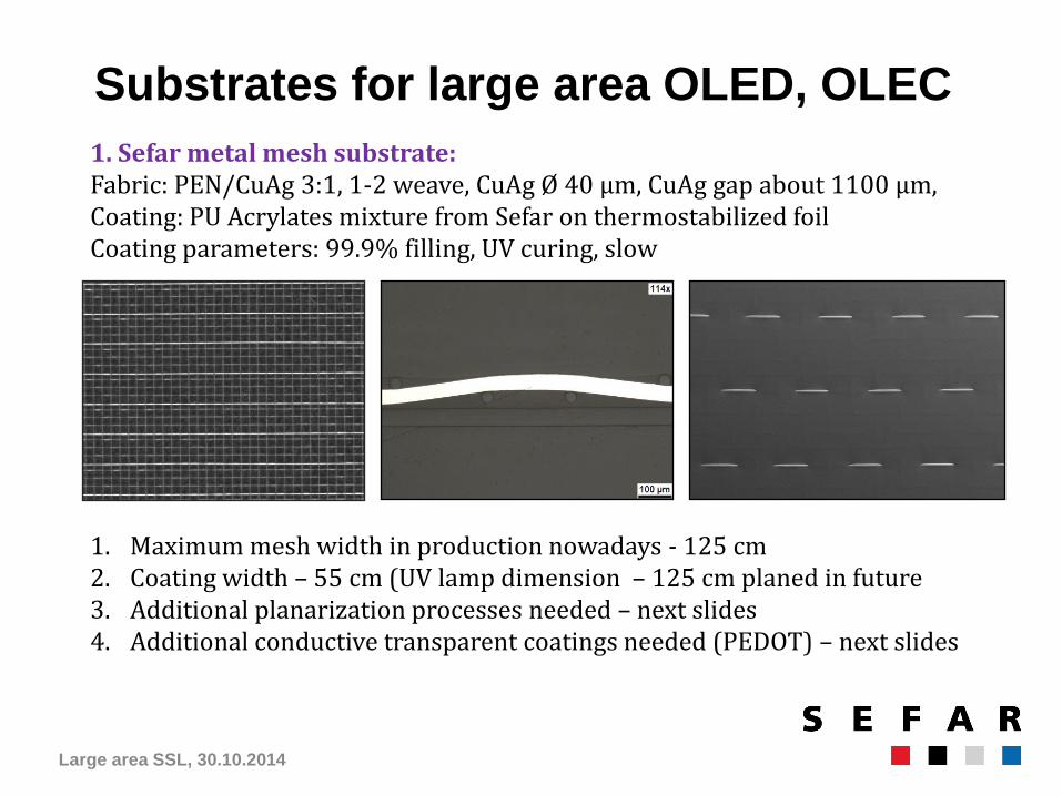
1. Sefar metal mesh substrate: Fabric: PEN/CuAg 3:1, 1-2 weave, CuAg Ø 40 μm, CuAg gap about 1100 μm, Coating: PU Acrylates mixture from Sefar on thermostabilized foil Coating parameters: 99.9% filling, UV curing, slow
1. Maximum mesh width in production nowadays - 125 cm 2. Coating width – 55 cm (UV lamp dimension – 125 cm planed in future 3. Additional planarization processes needed – next slides 4. Additional conductive transparent coatings needed (PEDOT) – next slides
Large area SSL, 30.10.2014

350 400 450 500 550 600 650 700 750
0
10
20
30
40
50
60
70
80
90
100
Wavelength (nm)
T %
V48_B
V47_C
V45_C
V45_D_K
V48_B direct
V47_C direct
V45_C direct
V45_D_K direct
Substrates for large area OLED, OLEC
Water (%) Polymer filler Cross linking
0.3 Standard PET
0.641 SEFAR – SF 1 Standard-UV
0.543 SEFAR – LF 1 Inert-UV
0.053 MX 004 Extrusion
0.024 MX 002 Extrusion
Light transmittance and water content
First samples already reached 85-87% transmittance in the visible range (400-800nm).
The latest generation of substrates shows increased transmittance by 2-3%.
A new polymer composition has a much lower water content. It has been tested at Fraunhofer IVV (Freising) and seems promising as a filling material for the fabric.
Large area SSL, 30.10.2014

PET Foil
SiOx
ORMOCER
SiOx
Sefar
coatings
Substrates for large area OLED, OLEC
The latest generation of substrates is produced in several steps incorporating SiOx-ORMOCER-SiOx barrier layers in the substrate.
Several materials for coating generation were already tested and analysed.
The most promising materials are under testing at Amcor and will be used for scale up processes. Additional components are under investigation and will be tested in the new CTI project with CSEM, starting on November 1st, 2014.
Large area SSL, 30.10.2014

Substrates for large area OLED, OLEC Additional plasma planarization processes realized
Rz ~ 10-15 µm
OLED devices fabricated using plain substrates present a high density of shorts, high leakage current and little light emission.
Results from KTI cooperation projects: WoCoLED Project no. 12055.1 PFNM-NM WoWLED Project no 13466.1 PFFLE-NM
Rz ~ 2-3 µm
Large area SSL, 30.10.2014

As a result of the planarization process, the leakage current is substantially reduced. This can be seen in Figure, where we present the total current (circles) and the fitted leakage current (solid red lines) of OLEDs made on non-planarised (left) and planarised (right) substrates. Even after planarization a certain number of shorts are still present.
Substrates for large area OLED, OLEC
Results from KTI cooperation projects: WoCoLED Project no. 12055.1 PFNM-NM WoWLED Project no 13466.1 PFFLE-NM
Large area SSL, 30.10.2014

Substrates for large area OLED, OLEC Additional conductive coating processes realized
Three types of conductive coatings were applied on the planarized Sefar substrates and the coated substrates were analysed.
Sample Coating R1 R2
V92 Cu/Ag40_850 PEDOT SV4 50 410
V93 Ag45-850 PEDOT SV4 20-80 400
V97 Cu/Ag40-1000 PEDOT SV4 20-80 370
PET Folie PEDOT SV4 370 370
V90 Cu/Ag45_1000 CNT 40 500
V90 Cu/Ag45_1000 AZO-Ag-AZO 0.2 8.5
Large area SSL, 30.10.2014

ELECTRICAL MEASUREMENTS PEDOT coated Sefar substrates have ca. 15 times better conductivity compared to PEDOT-coated PET film. CNT brings also considerable improvement at "only" 5% transmission loss. Plasma brings not only an improvement in conductivity, but also shows much better adhesion of the conductive layers. Nickel and copper appear badly with all electrical tests!
Substrates for large area OLED, OLEC
Large area SSL, 30.10.2014

Conductive layers (PEDOT:PSS, CNT,
TCO,…)
Generic fabric electrode layout for lab devices
PEDOT
Metallic wires
Generic fabric electrode layout for industrial application
Conductive wires in fabric:
Wire diameter 0,04mm Wires gap 0.5 -10 mm
Substrates for large area OLED, OLEC
Large area SSL, 30.10.2014

Construction scheme of the produced OLED on Sefar substrates temporary laminated on highly transparent glass plate.
Substrates for large area OLED, OLEC
1. The surface was plasma treated in order: - to remove residual layers formed on the metallic wires - to improve electrical contact between to the highly conductive PEDOT:PSS
2. Second PEDOT:PSS material was chosen as HTL layer based on its suitable WF for hole injection into the LEP (60 nm).
3. Poly (phenylvinylene) super-Yellow (SY, Merck Co., HOMO~-5.4eV, LUMO~3.0eV was dissolved in toluene, coated in glow-box and baked in a hot plate (~80nm).
4. The OLED devices were completed with a (3.5x4.0)cm2 cathode stack formed by 1nm LiF electron injection layer and 100 nm aluminum.
Results from KTI cooperation projects: WoCoLED Project no. 12055.1 PFNM-NM WoWLED Project no 13466.1 PFFLE-NM
Large area SSL, 30.10.2014

Flexible OLED devices fabricated on a SEFAR fabric-based electrode. On state at 1’000cd/m2 (~7Volts). Emissive area is 68 cm2. The device was not encapsulated and therefore operated under inert atmosphere.
Picture of an analogous device fabricated on ITO-coated glass at same voltage for comparison; the high sheet resistance of ITO results in a reduction in the emissive area.
Substrates for large area OLED, OLEC
Results from KTI cooperation projects: WoCoLED Project no. 12055.1 PFNM-NM WoWLED Project no 13466.1 PFFLE-NM
The high transparency and the low sheet resistance result in device performance of large-area devices similar to small-area devices made on e.g. ITO-coated glass.
68cm2
>1’000cd/m2
8.6 cd/A
Large area SSL, 30.10.2014

Current efforts are focused on engineering the substrate properties, OLED slot-die deposition processes and encapsulation solutions for roll-to-roll, flexible, large-area applications.
As a result of additional process development, SEFAR and CSEM have produced large-area (95cm2 emissive area), flexible OLED devices which demonstrated 3500cd/m2 and 12.1 cd/A at 10V.
Substrates for large area OLED, OLEC
Results from KTI cooperation projects: WoCoLED Project no. 12055.1 PFNM-NM WoWLED Project no 13466.1 PFFLE-NM
Large area SSL, 30.10.2014

Electroluminescence
OPV / OLED / Perovskite
Transparent Electrodes
Examples of using fabric based electrodes in optoelectronic industry
Substrates for large area OLED, OLEC
DSC
Large area SSL, 30.10.2014

CSEM, 4132 Muttenz, Switzerland
Marek Chrapa, Oscar Fernandez, Rolando Ferrini, Giovanni Nisato
Empa, 8600 Duebendorf, Switzerland
Frank Nüesch and his team
Sefar AG, 9425 Thal, Switzerland
Uriel Sonderegger, Murali Balakrishnan, Roland Blatter
…and you for your attention
Acknowledgement
Substrates for large area OLED, OLEC
Large area SSL, 30.10.2014