submicron features i n higher manganese silicide
TRANSCRIPT
Hindawi Publishing CorporationJournal of NanomaterialsVolume 2013, Article ID 701268, 5 pageshttp://dx.doi.org/10.1155/2013/701268
Research ArticleSubmicron Features in Higher Manganese Silicide
Yatir Sadia, Mor Elegrably, Oren Ben-Nun, Yossi Marciano, and Yaniv Gelbstein
Department of Materials Engineering, Ben-Gurion University of the Negev, Beer Sheva, Israel
Correspondence should be addressed to Yatir Sadia; [email protected]
Received 13 June 2013; Accepted 14 August 2013
Academic Editor: Jung-Kun Lee
Copyright © 2013 Yatir Sadia et al. This is an open access article distributed under the Creative Commons Attribution License,which permits unrestricted use, distribution, and reproduction in any medium, provided the original work is properly cited.
The world energy crisis had increased the demand for alternative energy sources and as such is one of the topics at the forefrontof research. One way for reducing energy consumption is by thermoelectricity. Thermoelectric effects enable direct conversion ofthermal into electrical energy. Higher manganese silicide (HMS, MnSi
1.75) is one of the promising materials for applications in the
field of thermoelectricity. The abundance and low cost of the elements, combined with good thermoelectric properties and highmechanical and chemical stability at high temperatures, make it very attractive for thermoelectric applications. Recent studies haveshown that Si-richHMS has improved thermoelectric properties.Themost interesting of which is the unusual reduction in thermalconductivity. In the current research, transmission (TEM) and scanning (SEM) electron microscopy as well as X-ray diffractionmethods were applied for investigation of the govern mechanisms resulting in very low thermal conductivity values of an Si-richHMS composition, following arc melting and hot-pressing procedures. In this paper, it is shown that there is a presence of sub-micron dislocations walls, stacking faults, and silicon and HMS precipitates inside each other apparent in the matrix, following ahigh temperature (0.9 Tm) hot pressing for an hour.These are not just responsible for the low thermal conductivity values observedbut also indicate the ability to create complicate nano-structures that will last during the production process and possibly duringthe application.
1. Introduction
Recent trends in clean energy have given rise to the needfor alternative energy sources. One such source is thermo-electric materials, which can utilize waste heat to increasethe efficiency of devices with high heat loss. The currentlyavailable thermoelectric materials are either not abundantenough formass production, expensive, toxic, or have too lowefficiency to be attractive.Themetal silicides are thermoelec-tric material with low production costs, made from abundantelements, nontoxic and highly stablematerials both thermallyand mechanically [1]. The most promising p-type materialsin this family are the higher manganese silicides (HMS)containing several very similar phases including Mn
4Si7,
Mn11Si19, Mn15Si26, andMn
27Si47[2]. While HMS offers one
of the fewmaterials which in addition to good thermoelectricproperties, low cost, and high abundance can also operate inatmospheric conditions [3, 4], it is yet not high enough inefficiency.
One of the most important measures to the efficiencyof a thermoelectric material is the dimensionless figure of
merit (ZT) defined as the square of Seebeck coefficienttimes the temperature over the electric resistivity time of thethermal conductivity.While the all three transport propertiesare related to the carrier concentration and are thereforeoptimized mainly by introducing an optimal amount ofcharge carriers into thematerials, research in the field showed[5] that ZT values can be also enhanced by increasing thestructure complexity and thereby decreasing the thermal con-duction by phonons without adversely affecting the chargecarrier concentration.
In recent publications, a low thermal conductivity wasrealized for HMS samples [6]. In the current research, theinfluence of apparent submicro features on reduction ofthe thermal conductivity, following an arc melting and hotpressing, was investigated.
2. Experimental Procedures
2.1. Synthesis. The samples were all synthesized from puresilicon (7N) and manganese (99.5%) pieces. The manganesepieces were cleaned using 50% hydrochloric acid and 50%
2 Journal of Nanomaterials
0102030405060708090
100
20 24 28 32 36 40 44 48 52 56 60 64 68 72 76 80
Inte
nsity
(AU
)
Arc melted sample
HMSSi
2𝜃 (∘)
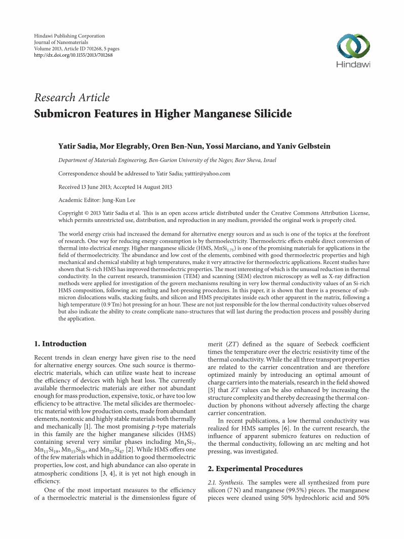
Figure 1: X-ray diffraction of eutectic arc melted specimen following hot pressing: e: silicon; ◼: higher manganese silicide peaks.
HMS
Si
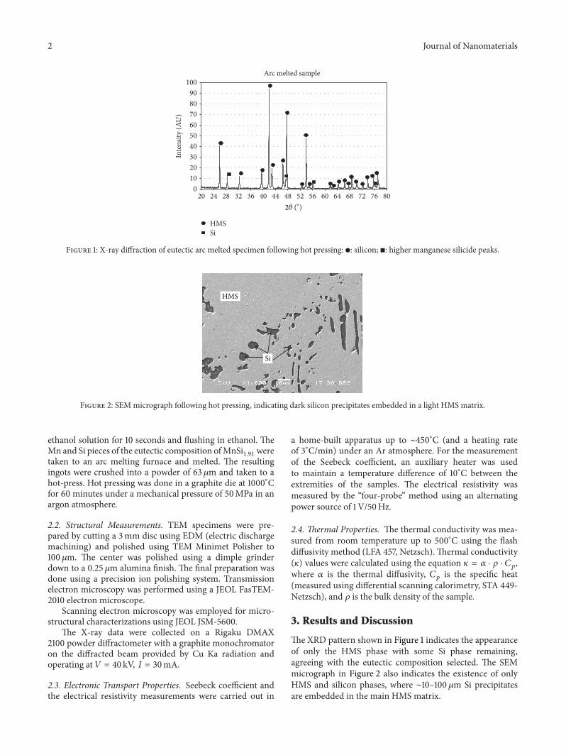
Figure 2: SEM micrograph following hot pressing, indicating dark silicon precipitates embedded in a light HMS matrix.
ethanol solution for 10 seconds and flushing in ethanol. TheMn and Si pieces of the eutectic composition ofMnSi
1.91were
taken to an arc melting furnace and melted. The resultingingots were crushed into a powder of 63𝜇m and taken to ahot-press. Hot pressing was done in a graphite die at 1000∘Cfor 60 minutes under a mechanical pressure of 50MPa in anargon atmosphere.
2.2. Structural Measurements. TEM specimens were pre-pared by cutting a 3mm disc using EDM (electric dischargemachining) and polished using TEM Minimet Polisher to100 𝜇m. The center was polished using a dimple grinderdown to a 0.25𝜇m alumina finish. The final preparation wasdone using a precision ion polishing system. Transmissionelectron microscopy was performed using a JEOL FasTEM-2010 electron microscope.
Scanning electron microscopy was employed for micro-structural characterizations using JEOL JSM-5600.
The X-ray data were collected on a Rigaku DMAX2100 powder diffractometer with a graphite monochromatoron the diffracted beam provided by Cu Ka radiation andoperating at 𝑉 = 40 kV, 𝐼 = 30mA.
2.3. Electronic Transport Properties. Seebeck coefficient andthe electrical resistivity measurements were carried out in
a home-built apparatus up to ∼450∘C (and a heating rateof 3∘C/min) under an Ar atmosphere. For the measurementof the Seebeck coefficient, an auxiliary heater was usedto maintain a temperature difference of 10∘C between theextremities of the samples. The electrical resistivity wasmeasured by the “four-probe” method using an alternatingpower source of 1 V/50Hz.
2.4. Thermal Properties. The thermal conductivity was mea-sured from room temperature up to 500∘C using the flashdiffusivity method (LFA 457, Netzsch). Thermal conductivity(𝜅) values were calculated using the equation 𝜅 = 𝛼 ⋅ 𝜌 ⋅ 𝐶
𝑝,
where 𝛼 is the thermal diffusivity, 𝐶𝑝is the specific heat
(measured using differential scanning calorimetry, STA 449-Netzsch), and 𝜌 is the bulk density of the sample.
3. Results and Discussion
The XRD pattern shown in Figure 1 indicates the appearanceof only the HMS phase with some Si phase remaining,agreeing with the eutectic composition selected. The SEMmicrograph in Figure 2 also indicates the existence of onlyHMS and silicon phases, where ∼10–100 𝜇m Si precipitatesare embedded in the main HMS matrix.
Journal of Nanomaterials 3
100 nm
(a)
Dislocationnet
100 nm
(b)
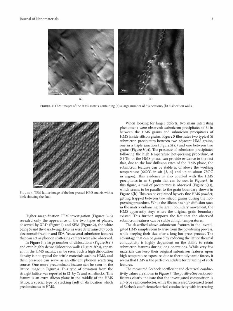
Figure 3: TEM images of the HMS matrix containing (a) a large number of dislocations, (b) dislocation walls.
2nm
Figure 4: TEM lattice image of the hot pressed HMS matrix with akink showing the fault.
Higher magnification TEM investigation (Figures 3–6)revealed only the appearance of the two types of phases,observed by XRD (Figure 1) and SEM (Figure 2), the whitebeing Si and the dark beingHMS, as were determined by bothelectrons diffraction andEDS. Yet, several submicron featuresthat can act as phonon scattering centers were also observed.
In Figure 3, a large number of dislocations (Figure 3(a))and even highly dense dislocation walls (Figure 3(b)), appar-ent in the HMS matrix, can be seen. Such a high dislocationdensity is not typical for brittle materials such as HMS, andtheir presence can serve as an efficient phonon scatteringsource. One more predominant feature can be seen in thelattice image in Figure 4. This type of deviation from thestraight lattice was reported in [2] by Ye and Amelinckx.Thisfeature is an extra silicon plane in the middle of the HMSlattice, a special type of stacking fault or dislocation whichpredominates in HMS.
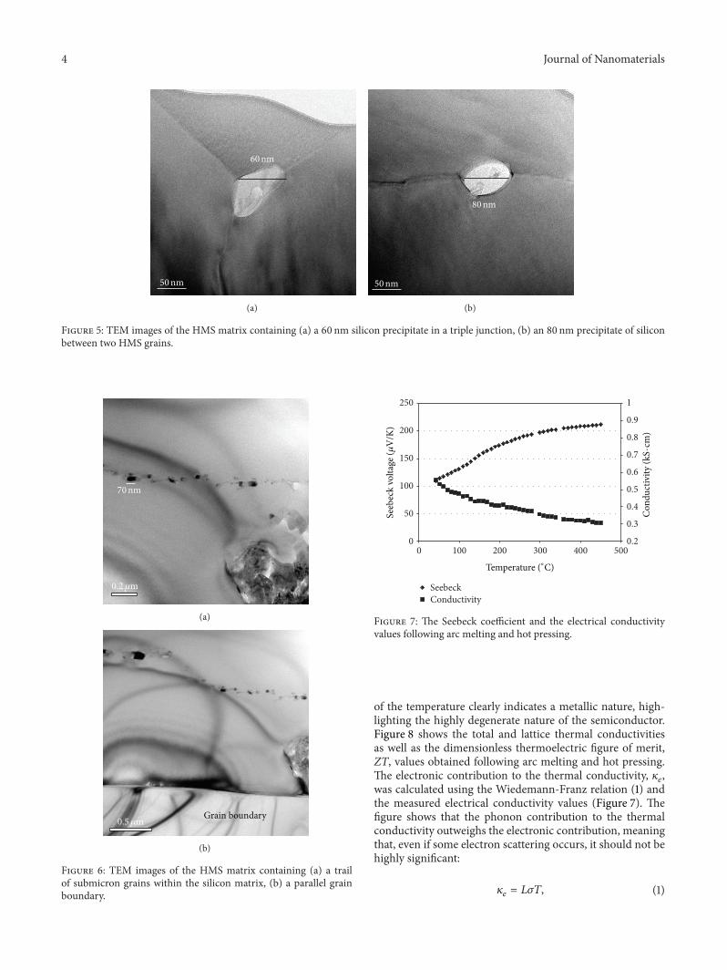
When looking for larger defects, two main interestingphenomena were observed: submicron precipitates of Si inbetween the HMS grains and submicron precipitates ofHMS inside silicon grains. Figure 5 illustrates two typical Sisubmicron precipitates between two adjacent HMS grains,one in a triple junction (Figure 5(a)) and one between twograins (Figure 5(b)). The presence of submicron precipitatesfollowing the high temperature hot-pressing procedure, at0.9 Tm of the HMS phase, can provide evidence to the factthat, due to the low diffusion rates of the HMS phase, thesubmicron features can be stable at or above the workingtemperature (660∘C in air [3, 4] and up to about 750∘Cin argon). This evidence is also coupled with the HMSprecipitates in an Si grain that can be seen in Figure 6. Inthis figure, a trail of precipitates is observed (Figure 6(a)),which seems to be parallel to the grain boundary shown inFigure 6(b). This can be explained by very fine HMS powder,getting trapped between two silicon grains during the hot-pressing procedure. While the silicon has high diffusion ratesin the matrix enhancing the grain boundary movement, theHMS apparently stays where the original grain boundaryexisted. This further supports the fact that the observedsubmicron features can be stable at high temperatures.
The described above submicron features in the investi-gatedHMS sample seem to arise from the powdering process,while keeping their size after a long hot-press process. Theadvantage that can be gained by reducing the lattice thermalconductivity is highly dependent on the ability to retainsubmicron features during long operations. While very fewmaterials can keep their original submicron features uponhigh temperature exposure, due to thermodynamic forces, itseems that HMS is the perfect candidate for retaining of suchfeatures.
The measured Seebeck coefficient and electrical conduc-tivity values are shown in Figure 7.The positive Seebeck coef-ficients clearly indicate that the investigated composition isa p-type semiconductor, while the increased/decreased trendof Seebeck coefficient/electrical conductivity with increasing
4 Journal of Nanomaterials
60nm
50nm
(a)
80nm
50nm
(b)
Figure 5: TEM images of the HMS matrix containing (a) a 60 nm silicon precipitate in a triple junction, (b) an 80 nm precipitate of siliconbetween two HMS grains.
70nm
0.2 𝜇m
(a)
0.5 𝜇m Grain boundary
(b)
Figure 6: TEM images of the HMS matrix containing (a) a trailof submicron grains within the silicon matrix, (b) a parallel grainboundary.
0.2
0.3
0.4
0.5
0.6
0.7
0.8
0.9
1
0
50
100
150
200
250
0 100 200 300 400 500
SeebeckConductivity
Con
duct
ivity
(kS·
cm)
Temperature (∘C)
Seeb
eck
volta
ge (𝜇
V/K
)
Figure 7: The Seebeck coefficient and the electrical conductivityvalues following arc melting and hot pressing.
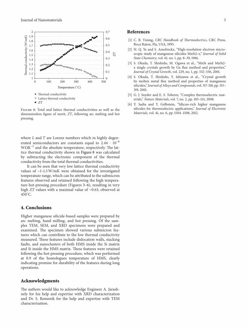
of the temperature clearly indicates a metallic nature, high-lighting the highly degenerate nature of the semiconductor.Figure 8 shows the total and lattice thermal conductivitiesas well as the dimensionless thermoelectric figure of merit,ZT, values obtained following arc melting and hot pressing.The electronic contribution to the thermal conductivity, 𝜅
𝑒,
was calculated using the Wiedemann-Franz relation (1) andthe measured electrical conductivity values (Figure 7). Thefigure shows that the phonon contribution to the thermalconductivity outweighs the electronic contribution, meaningthat, even if some electron scattering occurs, it should not behighly significant:
𝜅𝑒= 𝐿𝜎𝑇, (1)
Journal of Nanomaterials 5
0
0.1
0.2
0.3
0.4
0.5
0.6
0.7
11.11.21.31.41.51.61.71.81.9
2
ZT
Ther
mal
cond
uctiv
ity (W
/mK)
Thermal conductivityLattice thermal conductivityZT
0 100 200 300 400 500
Temperature (∘C)
Figure 8: Total and lattice thermal conductivities as well as thedimensionless figure of merit, ZT, following arc melting and hotpressing.
where 𝐿 and 𝑇 are Lorenz numbers which in highly degen-erated semiconductors are constants equal to 2.44 ⋅ 10−8WΩK−2 and the absolute temperature, respectively. The lat-tice thermal conductivity shown in Figure 8 was calculatedby subtracting the electronic component of the thermalconductivity from the total thermal conductivities.
It can be seen that very low lattice thermal conductivityvalues of ∼1–1.3W/mK were obtained for the investigatedtemperature range, which can be attributed to the submicronfeatures observed and retained following the high tempera-ture hot-pressing procedure (Figures 3–6), resulting in veryhigh ZT values with a maximal value of ∼0.63, observed at450∘C.
4. Conclusions
Higher manganese silicide-based samples were prepared byarc melting, hand milling, and hot pressing. Of the sam-ples TEM, SEM, and XRD specimens were prepared andexamined. The specimen showed various submicron fea-tures which can contribute to the low thermal conductivitymeasured. These features include dislocation walls, stackingfaults, and nanoclusters of both HMS inside the Si matrixand Si inside the HMS matrix. These features were retainedfollowing the hot-pressing procedure, which was performedat 0.9 of the homologues temperature of HMS, clearlyindicating promise for durability of the features during longoperations.
Acknowledgments
The authors would like to acknowledge Engineer A. Jarash-nely for his help and expertise with XRD characterizationand Dr. S. Remenik for the help and expertise with TEMcharacterization.
References
[1] C. B. Vining, CRC Handbook of Thermoelectrics, CRC Press,Boca Raton, Fla, USA, 1995.
[2] H. Q. Ye and S. Amelinckx, “High-resolution electron micro-scopic study of manganese silicides MnSi2-x,” Journal of SolidState Chemistry, vol. 61, no. 1, pp. 8–39, 1986.
[3] S. Okada, T. Shishido, M. Ogawa et al., “MnSi and MnSi2-x single crystals growth by Ga flux method and properties,”Journal of Crystal Growth, vol. 229, no. 1, pp. 532–536, 2001.
[4] S. Okada, T. Shishido, Y. Ishizawa et al., “Crystal growthby molten metal flux method and properties of manganesesilicides,” Journal of Alloys andCompounds, vol. 317-318, pp. 315–319, 2001.
[5] G. J. Snyder and E. S. Toberer, “Complex thermoelectric mat-erials,” Nature Materials, vol. 7, no. 2, pp. 105–114, 2008.
[6] Y. Sadia and Y. Gelbstein, “Silicon-rich higher manganesesilicides for thermoelectric applications,” Journal of ElectronicMaterials, vol. 41, no. 6, pp. 1504–1508, 2012.

Submit your manuscripts athttp://www.hindawi.com
ScientificaHindawi Publishing Corporationhttp://www.hindawi.com Volume 2014
CorrosionInternational Journal of
Hindawi Publishing Corporationhttp://www.hindawi.com Volume 2014
Polymer ScienceInternational Journal of
Hindawi Publishing Corporationhttp://www.hindawi.com Volume 2014
Hindawi Publishing Corporationhttp://www.hindawi.com Volume 2014
CeramicsJournal of
Hindawi Publishing Corporationhttp://www.hindawi.com Volume 2014
CompositesJournal of
NanoparticlesJournal of
Hindawi Publishing Corporationhttp://www.hindawi.com Volume 2014
Hindawi Publishing Corporationhttp://www.hindawi.com Volume 2014
International Journal of
Biomaterials
Hindawi Publishing Corporationhttp://www.hindawi.com Volume 2014
NanoscienceJournal of
TextilesHindawi Publishing Corporation http://www.hindawi.com Volume 2014
Journal of
NanotechnologyHindawi Publishing Corporationhttp://www.hindawi.com Volume 2014
Journal of
CrystallographyJournal of
Hindawi Publishing Corporationhttp://www.hindawi.com Volume 2014
The Scientific World JournalHindawi Publishing Corporation http://www.hindawi.com Volume 2014
Hindawi Publishing Corporationhttp://www.hindawi.com Volume 2014
CoatingsJournal of
Advances in
Materials Science and EngineeringHindawi Publishing Corporationhttp://www.hindawi.com Volume 2014
Smart Materials Research
Hindawi Publishing Corporationhttp://www.hindawi.com Volume 2014
Hindawi Publishing Corporationhttp://www.hindawi.com Volume 2014
MetallurgyJournal of
Hindawi Publishing Corporationhttp://www.hindawi.com Volume 2014
BioMed Research International
MaterialsJournal of
Hindawi Publishing Corporationhttp://www.hindawi.com Volume 2014
Nano
materials
Hindawi Publishing Corporationhttp://www.hindawi.com Volume 2014
Journal ofNanomaterials