study on passive intermodulation (pim) in microwave filters1188388/fulltext01.pdf · dispositivos...
TRANSCRIPT

IN DEGREE PROJECT ELECTRICAL ENGINEERING,SECOND CYCLE, 30 CREDITS
, STOCKHOLM SWEDEN 2018
Study on Passive Intermodulation (PIM) in Microwave FiltersDouble Degree Program KTH-UPM
IRENE ORTIZ DE SARACHO PANTOJA
KTH ROYAL INSTITUTE OF TECHNOLOGYSCHOOL OF ENGINEERING SCIENCES


Master Thesis Report
Title: Study on Passive Intermodulation (PIM) in
Microwave Filters
Author: Irene Ortiz de Saracho Pantoja
Supervisors: Prof. Urban Westergren (KTH)
Esa Myllyvainio (Microdata Telecom AB)
Jakob Petrén (Microdata Telecom AB)
Affiliation 1: School of Engineering Sciences
School of Electrical Engineering and Com-
puter Science
KTH Royal Institute of Technology
Affiliation 2: ETS de Ingenieros de Telecomunicación
Universidad Politécnica de Madrid
TRITA: SCI-GRU 2018:019
Thesis Committee
President: Prof. Urban Westergren
Member: Johan Richard Schatz
Opponent: Carlos Gonzalo Peces
Stockholm, 5th of March, 2018


i
Abstract
Passive Intermodulation (PIM) is a crucial problem in communication sys-tems where high power is involved and the transmitter and receiver areclose. Intermodulation products created by devices considered as linear aredifficult to predict and impossible to suppress, since they appear after thefiltering stage.
Manufacturing issues such as loose connections or metal particles areusually behind PIM generation. However, there are other causes such asmetal junctions or electrothermal effects which can also be enhanced by thephysical structures or the design. This work aims to study and propose prac-tical ways to improve PIM performance to be implemented during the de-sign stage. In particular, microwave filters for mobile communications areaddressed.
Since PIM generation is a current-related non-linearity, one approach tostudy it is to evaluate the current density distribution in the resonant cavitiestypically used for mobile communication filters.
Besides, the introduction of a PIM source as a circuital element in a fil-tering network helps to evaluate how topology, bandwidth or filter responsemay affect the interference levels. Several structures are analysed, from sim-ple all-pole filters to diplexers including transmission-zero responses.
The conclusions obtained in this work may help to take design decisions,keeping PIM control in mind. Future work lines are also proposed, aimingto go in depth in the derived results.
This Thesis has been developed in cooperation with Microdata TelecomAB.
Keywords: PIM, microwave filters, coaxial cavity resonators, non-linearinductor


iii
Sammanfattning
Passiv intermodulation (PIM) är ett viktigt problem i kommunikationssys-tem som utnyttjar högeffekt och där sändaren och mottagaren är nära placer-ade. Intermodulationsprodukter uppkommer i enheter som är att betraktasom linjära, och blir därför svåra att förutsäga. De är också omöjliga attundertrycka, eftersom de kan uppträda filtreringssteget och ofta faller inompassbandet.
Tillverkningsproblem som lösa kontaktanslutningar eller metallpartiklarär vanliga PIM källor i passiva komponenter. Det finns emellertid andra or-saker, till exempel metallövergångar eller elektrotermiska effekter, som kanförbättras av den fysiska utformningen. Detta arbete syftar till att studera ochföreslå praktiska sätt att förbättra PIM-prestanda redan under designfasen.Arbetet adresserar speciellt mikrovågsfilter för mobil kommunikation.
PIM-generering är en strömrelaterad olinjäritet. Studien har därför un-dersökt strömtäthetsfördelningen i de resonanskaviteter som vanligtvis an-vänds i mobilkommunikationsfilter.
Dessutom har en lumpad PIM-källa utvecklats för att möjlig göra kretssimu-leringar av hur filtertopolgin, bandbredd och filterrespons påverkar interfer-ensnivåerna. Enkla flerpoliga filter med och utan transmissionsnollor harundersökts. Även sammansatta combiner- och diplexfilter har studerats medhjälp av den lumpade PIM-källan.
Slutsatserna av arbetet kan bidra till att fatta bättre designbeslut medavseende på PIM-prestanda. Framtida arbetsområden föreslås också, somsyftar till att gå djupare i de presenterade resultaten.
Denna rapport framställdes i samarbete med Microdata Telecom AB.
Nyckelord: PIM, mikrovågsfilter, coaxial resonanshåligheter, olinjär in-duktor


v
Resumen
La Intermodulación Pasiva (PIM) es un problema importante en sistemas decomunicación donde hay involucrada mucha potencia y el transmisor y elreceptor se encuentran cerca. Los productos de intermodulación creados pordispositivos considerados lineales son difíciles de predecir e imposibles desuprimir, puesto que aparecen después de la etapa de filtrado.
Detrás de la PIM suele haber problemas de fabricación, como conexionessueltas o partículas de metal. No obstante, exiten otras causas como lasuniones metálicas o efectos electrotérmicos que pueden ser amplificados porla propia estructura física del diseño. Este trabajo está centrado en estudiary proponer técnicas prácticas de mejorar el rendimiento en términos de PIMque puedan ser implementadas en la fase de diseño. En concreto, se analizanlos filtros de microondas para aplicaciones de comunicaciones móviles.
Dado que la generación de PIM está relacionada con no-linealidades de-pendientes de la corriente, uno de los enfoques es evaluar la distribución dela densidad de corriente en las cavidades resonantes utilizadas en este tipode filtros.
Además, la introducción de una fuente de PIM como elemento circuital enun filtro puede ayudar a estudiar los efectos en los niveles de interferencia dela topología, el ancho de banda o la propia respuesta del filtro. Se analizanvarias estructuras, desde filtros sencillos con respuesta all-pole a diplexoresque incluyen filtros con ceros de transmisión.
Las conclusiones obtenidas en este trabajo pueden ayudar a la hora detomar decisiones de diseño, teniendo en mente el control de PIM. Además,se proponen otras líneas futuras de trabajo, con el objetivo de profundizar enlos resultados.
Este Trabajo Fin de Master se ha desarrollado en colaboración con Micro-data Telecom AB.
Palabras clave: PIM, filtros de microondas, cavidades coaxiales resonantes,inductor no lineal


vii
Acknowledgements
An incommensurable number of people have stepped into my life duringthese years. Some of them have always been there, others appeared quietlyand then turned everything upside down, and others are already gone. Butall of them have left a mark on me and I think it is a good moment to expressmy gratitude.
First, I would like to thank Microdata for giving me the opportunity ofdoing this project with them, in particular to my supervisors Esa and Jakob.Their help and availability were key for the work, specially in an obscurefield such as this one. Special thanks to Jakob for caring so much about meevery day. I would also like to acknowledge Johan, for his invaluable insightand concern, and Petri, for taking the time to deal with all the software issuesimaginable. Besides, I have been very lucky to count with the supervisionfrom KTH of Urban Westergren, always involved in the project even from adifferent continent.
These sixteen months in Sweden would have been very different withoutall the people who I have met here. I cannot express enough how grateful Ifeel for the opportunity of sharing a bit of Sweden with you: the ones whoare still here (Guayén, Pablo, Neelu, Per Olof, Emil and the people at the Lan-guage Café) and those who already left (Sebastian, Vicent, Thomas, Michael,Ángela, Viktor...). When being alone in a different country, 3000 km awayfrom my comfort zone, you made me feel at home.
Two more people clearly stand out. Carlos: we began this journey to-gether seven years ago (are we really that old?) and we will finish it togetheras well. I admire you enormously and I am sure you will be a fantastic engi-neer... at least as much as the wonderful friend you are. Enrique: I have hadto move 10 times the distance between Madrid and Jaén to find you, so donot count on me letting you go. Thank you for giving light and love to thedark days and making brighter the sunny ones.
Now that I will be a proper telecommunications engineer, I need to thankall the people from my second home in Madrid, la Escuela, who have taughtme everything I know. I have spent there more hours than I can rememberand I have made priceless friends: Alberto, Jorge, Cris, Marta, Natalia...

viii
My infinite gratitude will always be for José Ramón. Whatever I achieveprofessionally in the future, it will be because of you. Thank you for openingthe door to a magic world and for being such an example. Ezina ekinez egina,although that is not very valued nowadays.
I would like to remember Mariano as well, because no one who knew himcould remain indifferent.
Finally, I would like to say thank you to my whole family, and also tothose friends who have become family: papá, los yayes, las tías, el grupo. I havealways felt blessed and loved with you. Your support travels through timeand distance.
I finish with the two people who are indeed the beginning of everything.Lulú: I am extremely proud of you and I believe that our differences arestrengthening in some way. I love you, and I write it down so that you canread it whenever you need. Mamá: you are the person I admire the most andyou will be part of everything I will do in my life. Thank you for letting mefly, but also for waiting at the nest when I need to come back.

ix
Contents
Abstract i
Sammanfattning iii
Resumen v
Acknowledgements vii
1 Introduction 11.1 Problem statement . . . . . . . . . . . . . . . . . . . . . . . . . 11.2 Objectives . . . . . . . . . . . . . . . . . . . . . . . . . . . . . . 2
2 Background and Literature Review 52.1 Introduction to PIM . . . . . . . . . . . . . . . . . . . . . . . . . 52.2 Measurement . . . . . . . . . . . . . . . . . . . . . . . . . . . . 72.3 Sources . . . . . . . . . . . . . . . . . . . . . . . . . . . . . . . . 8
2.3.1 Contact . . . . . . . . . . . . . . . . . . . . . . . . . . . . 92.3.2 Thermal effects . . . . . . . . . . . . . . . . . . . . . . . 102.3.3 Materials . . . . . . . . . . . . . . . . . . . . . . . . . . . 112.3.4 Structure . . . . . . . . . . . . . . . . . . . . . . . . . . . 11
2.4 Identification of PIM sources . . . . . . . . . . . . . . . . . . . 122.5 PIM Modelling . . . . . . . . . . . . . . . . . . . . . . . . . . . 122.6 Other aspects . . . . . . . . . . . . . . . . . . . . . . . . . . . . 13
2.6.1 Input power . . . . . . . . . . . . . . . . . . . . . . . . . 132.6.2 Effect of impedance . . . . . . . . . . . . . . . . . . . . 142.6.3 Time dependence . . . . . . . . . . . . . . . . . . . . . . 14
2.7 Conclusions . . . . . . . . . . . . . . . . . . . . . . . . . . . . . 14
3 Current Analysis in Coaxial Resonators 173.1 Motivation . . . . . . . . . . . . . . . . . . . . . . . . . . . . . . 173.2 Foundations of coaxial resonators . . . . . . . . . . . . . . . . . 183.3 Coaxial cavity resonator with hat . . . . . . . . . . . . . . . . . 19
3.3.1 Electromagnetic fields and current density . . . . . . . 20

x
3.3.2 Cavity resonator model. Analysis setup. . . . . . . . . 213.4 Disc junction: Variation over the coaxial cavity resonator with
hat . . . . . . . . . . . . . . . . . . . . . . . . . . . . . . . . . . . 253.5 Coupled resonators . . . . . . . . . . . . . . . . . . . . . . . . . 273.6 In-coupling structures . . . . . . . . . . . . . . . . . . . . . . . 293.7 Conclusions . . . . . . . . . . . . . . . . . . . . . . . . . . . . . 30
4 Circuital Model of PIM Sources 334.1 Motivation . . . . . . . . . . . . . . . . . . . . . . . . . . . . . . 334.2 PIM source models . . . . . . . . . . . . . . . . . . . . . . . . . 34
4.2.1 External non-linear element as a PIM source . . . . . . 354.2.2 Internal non-linear element as a PIM source . . . . . . 36
4.3 Non-Linear Inductor (NLI) as a PIM source . . . . . . . . . . . 364.3.1 IM products with NLI . . . . . . . . . . . . . . . . . . . 374.3.2 NLI coefficient determination . . . . . . . . . . . . . . . 38
4.4 Placement of PIM sources at filtering networks . . . . . . . . . 394.5 Conclusions . . . . . . . . . . . . . . . . . . . . . . . . . . . . . 40
5 Circuital Analysis of Filters with PIM sources 415.1 Motivation . . . . . . . . . . . . . . . . . . . . . . . . . . . . . . 415.2 Analysis setup and considerations . . . . . . . . . . . . . . . . 425.3 Single filter analysis . . . . . . . . . . . . . . . . . . . . . . . . . 44
5.3.1 All-pole filter . . . . . . . . . . . . . . . . . . . . . . . . 445.3.2 Filters with one transmission zero . . . . . . . . . . . . 46
Positive cross-coupling . . . . . . . . . . . . . . . . . . . 46Negative cross-coupling . . . . . . . . . . . . . . . . . . 50Other variations: bandwidth . . . . . . . . . . . . . . . 51
5.4 Example: complex structures and reflected PIM . . . . . . . . 52Filter 1 . . . . . . . . . . . . . . . . . . . . . . . . . . . . 53Filter 2 . . . . . . . . . . . . . . . . . . . . . . . . . . . . 55Diplexer . . . . . . . . . . . . . . . . . . . . . . . . . . . 56
5.5 Conclusions . . . . . . . . . . . . . . . . . . . . . . . . . . . . . 59
6 Conclusion 616.1 Conclusions . . . . . . . . . . . . . . . . . . . . . . . . . . . . . 61
6.1.1 Current analysis in coaxial resonators . . . . . . . . . . 626.1.2 Circuital model of PIM sources and analysis of filtering
networks . . . . . . . . . . . . . . . . . . . . . . . . . . . 626.2 Future work . . . . . . . . . . . . . . . . . . . . . . . . . . . . . 63

xi
A Introduction to filter design 65A.1 Filter parameters . . . . . . . . . . . . . . . . . . . . . . . . . . 65A.2 Low-pass to bandpass transformation . . . . . . . . . . . . . . 66A.3 Transmission zeros . . . . . . . . . . . . . . . . . . . . . . . . . 67A.4 Insertion losses and Q value . . . . . . . . . . . . . . . . . . . . 69A.5 Group delay . . . . . . . . . . . . . . . . . . . . . . . . . . . . . 70


xiii
List of Figures
2.1 Output spectrum when two tones f1, f2 are applied to a non-linear system . Figure taken from P.L.Lui, ”Passive Intermodula-tion Interference in Communication Systems”[3] . . . . . . . . . . 5
2.2 PIM scenario A (Transmitted PIM) . . . . . . . . . . . . . . . . 72.3 PIM scenario B (Reflected PIM) . . . . . . . . . . . . . . . . . . 72.4 Block diagram of the PIM measurement setup [6] . . . . . . . 82.5 a) Contact of two metallic plates b) Enhanced view of the junc-
tion c) Approximate model using steps. Figure taken from J.Russer et al., ”Phenomenological Modeling of Passive Intermodula-tion due to Electron Tunneling at Metallic Contacts” [9] . . . . . . 10
2.6 Equivalent representation of a cavity, with ro assumed non-linear. Figure taken from G. Macchiarella et al., ”Passive Intermod-ulation in Microwave Filters: Experimental Investigation” [18] . . 12
3.1 λ/4 coaxial resonator: (A) single cavity, (B) equivalent circuitand (C) cavity with tuning screw. . . . . . . . . . . . . . . . . . 18
3.2 Coaxial resonator with hat . . . . . . . . . . . . . . . . . . . . . 193.3 Electromagnetic fields at the resonant frequency for the coaxial
cavity with hat . . . . . . . . . . . . . . . . . . . . . . . . . . . . 203.4 Surface current density in the inner cylinder of the cavity:(A)
vector, (B) magnitude. Colours from red (highest value) toblue (lowest). . . . . . . . . . . . . . . . . . . . . . . . . . . . . 20
3.5 Cross-sectional view of the cavity resonator. Junction in dashedline. . . . . . . . . . . . . . . . . . . . . . . . . . . . . . . . . . . 21
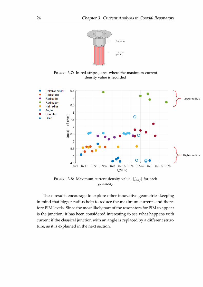
3.6 Diagram of modifications 5 and 6 . . . . . . . . . . . . . . . . . 223.7 In red stripes, area where the maximum current density value
is recorded . . . . . . . . . . . . . . . . . . . . . . . . . . . . . . 243.8 Maximum current density value, |Jsur f | for each geometry . . 243.9 Analysed options for the junction . . . . . . . . . . . . . . . . . 253.10 Cross-sectional view of the cavity resonator with markers M1,
M2 . . . . . . . . . . . . . . . . . . . . . . . . . . . . . . . . . . . 26

xiv
3.11 In white, area where the maximum current density value isrecorded . . . . . . . . . . . . . . . . . . . . . . . . . . . . . . . 26
3.12 Variation in current density, |Jsur f |, between markers M1 andM2 for each geometry . . . . . . . . . . . . . . . . . . . . . . . . 27
3.13 Equivalent coupling situations for two coaxial cavity resonators 283.14 Two in-coupling configurations for coaxial cavity resonators . 293.15 Current density peaks for in-coupling configurations from Fig-
ure 3.14 . . . . . . . . . . . . . . . . . . . . . . . . . . . . . . . . 30
4.1 Four different ideas to include a PIM source in a linear circuit.f1 and f2 belong to the passband. . . . . . . . . . . . . . . . . . 34
4.2 Circuital PIM source model with diode . . . . . . . . . . . . . 354.3 Genesys model of a non-linear inductor (NLI) . . . . . . . . . 374.4 PIM source measurement simulation setup . . . . . . . . . . . 394.5 Possible locations of PIM sources in a filter . . . . . . . . . . . 39
5.1 Examples of PIM scenarios in mobile communications filterapplications . . . . . . . . . . . . . . . . . . . . . . . . . . . . . 42
5.2 Explanation of the typical PIM plots included in this work . . 435.3 S-parameters and group delay for the all-pole filter . . . . . . 445.4 PIM levels for the all-pole filter with non-linear resonators . . 455.5 Peak current at the resonators . . . . . . . . . . . . . . . . . . . 465.6 S-parameters and group delay for the 6-1 filter with positive
cross-coupling . . . . . . . . . . . . . . . . . . . . . . . . . . . . 475.7 Six different topologies to implement the response in Figure 5.7 475.8 PIM levels measured at the output (L) for the 6-1 filter with
positive cross-coupling . . . . . . . . . . . . . . . . . . . . . . . 485.9 Peak current in jumped resonators for topologies A,B and C . 495.10 S-parameters and group delay for the 6-1 filter with negative
cross-coupling . . . . . . . . . . . . . . . . . . . . . . . . . . . . 505.11 PIM level for the 6-1 filter with negative coupling . . . . . . . 505.12 S-parameters and group delay for the 6-1 filter with positive
coupling and double bandwidth . . . . . . . . . . . . . . . . . 515.13 Comparison of PIM levels for 6-1 filters with positive coupling
and different bandwidth (75 vs 150MHz) . . . . . . . . . . . . 525.14 Diagram of the diplexer . . . . . . . . . . . . . . . . . . . . . . 525.15 Frequency bands of the diplexer . . . . . . . . . . . . . . . . . 535.16 S-parameters of Filter 1 . . . . . . . . . . . . . . . . . . . . . . . 545.17 Frequency spectrum for filter 1 . . . . . . . . . . . . . . . . . . 54

xv
5.18 PIM values for filter 1 f1 fixed to 1805 MHz . . . . . . . . . . . 555.19 S-parameters of Filter 2 . . . . . . . . . . . . . . . . . . . . . . . 555.20 Diagram of the diplexer including the directional couplers and
port naming . . . . . . . . . . . . . . . . . . . . . . . . . . . . . 565.21 Genesys schematic for the diplexer . . . . . . . . . . . . . . . . 565.22 Diplexer frequency spectrum when there are input tones from
both TX filters . . . . . . . . . . . . . . . . . . . . . . . . . . . . 57
A.1 Working flow for filter design . . . . . . . . . . . . . . . . . . . 65A.2 Example of Chebychev low-pass prototype, N=4 . . . . . . . . 66A.3 Example of Chebychev bandpass filter . . . . . . . . . . . . . . 66A.4 Diagram of a Chebychev fourth-order filter . . . . . . . . . . . 67A.5 S-parameters of a fourth-order Chebychev filter . . . . . . . . 67A.6 S-parameters of a fourth-order Chebychev filter with one TZ . 68A.7 Diagram of a Chebychev fourth-order filter with one TZ . . . 68A.8 Chebychev bandpass filter with cross-coupling . . . . . . . . . 68A.9 Parallel resonant circuit including losses . . . . . . . . . . . . . 69A.10 Group delay characteristic for the filter in Figure A.10 . . . . . 70


xvii
List of Tables
2.1 Summary of references for the literature review . . . . . . . . . 15
3.1 Summary of the geometrical variations of the cavity. Variablesreferred according to Figure 3.5. Values in millimetres. . . . . 23
3.2 Summary of the geometrical variations of the disc. Variablesreferred according to Figure 3.10. Values in millimetres. . . . . 27
3.3 Comparison between coupling situations from Figure 3.13 . . 28
5.1 Diplexer PIM levels . . . . . . . . . . . . . . . . . . . . . . . . . 58


xix
List of Abbreviations
IM InterModulationPIM Passive InterModulationAM-PM Amplitude-to-PhaseTX Transmitter,TransmissionRX Receiver, ReceptionDUT Device Under TextLNA Low Noise AmplifierSA Spectrum AnalyserNLI Non-Linear InductorTZ Transmission Zero


xxi
Para M, siempre.Para E, por siempre.


1
Chapter 1
Introduction
1.1 Problem statement
One of the words that describes best our world nowadays is ”connectivity”.Being connected has moved from an advantage to a real need, as the increas-ing number of mobile phone users show. Only in Sweden, 98% of the pop-ulation own a mobile phone, and 85% have a smartphone [1]. If a globalperspective is considered, smartphones will be used by more than a third ofthe global population by the end of the current year [2]. Such increase ofusers and the growing data rates demanded make critical the developmentof the network components.
Such a hyper-connected environment emphasizes traditional communi-cation problems, for example interference, which is a basic issue encounteredfrom the very beginning of communication. The term refers to the addition ofunwanted signals to a useful signal. Interference becomes more critical whenthe two key resources - frequency and power - are pushed to their limits.
Firstly, the frequency spectrum is finite and there is a great number ofapplications sharing it. Therefore it is not possible to use it carelessly, sincefrequency bands for different applications are very close. Interference levelsmust be kept low so that they do not disturb neighbour services performance.
Besides, interferences have an impact on the number of users granted aservice. The minimum power required to obtain a certain capacity, i.e. sen-sitivity, increases in presence of interferences. In other words, more poweris required to provide the same capacity. If the power level is set, the conse-quence is that less users can access the service.
As a result, interference generation and control is a widely studied field.Moreover, the future of mobile communications and the rising of other areassuch as Internet of Things (IoT) allow to predict a continuing interest in thearea.

2 Chapter 1. Introduction
Within the field of interference generation, there is one distortion phe-nomenon known as intermodulation (IM). It is caused when two or moresignals are mixed through a non-linear characteristic and originate spurioussignals (IM products) at other frequencies [3]. Non-linear systems are typ-ically made out of active elements, such as amplifiers. They have a knownnon-linear response, which can be described and controlled, and so can bethe new generated signals.
However, some intermodulation processes cannot be precisely described,like the so-called passive intermodulation. Passive Intermodulation (PIM) isa type of distortion consisting in the generation of intermodulation productsin devices whose response is thought of as linear. The main characteristic ofPIM is that it appears in passive devices like cables, connectors or filters. Inthis case, the intrinsic non-linearity is so weak that it should not be detected,yet it appears.
PIM has been a difficult issue for many years in communication systems.In this Thesis, the focus is on microwave filters, in particular those used formobile communication applications. It is a field where PIM requirements forthe equipment involved are becoming more critical, due to the strict restric-tions in terms of frequency and system sensitivity.
1.2 Objectives
The main goal of this Thesis is to study and propose practical ways to improvePIM performance in microwave filters to be implemented during the design stage.
As it will be described, PIM is a very heuristic problem and it greatlydepends on the manufacturing process. Consequently, that is the stage wherePIM is usually encountered and handled. However, it is worth studying ifsome small variations throughout the design stage may help to reduce theexpected PIM floor level. In other words, if the manufacturing process isconsidered to be the same, it is interesting to test if some geometries or designprocedures favour PIM generation more than others.
In order to fulfil the main task, the first step is to carry out a literaturereview, specially when dealing with such a broad field as PIM. This phe-nomenon has been studied in the last decades taking many different perspec-tives. From practical experiments to complex models, aiming to determinethe main source or even how PIM varies with time. This analysis allows tonarrow down the Thesis approach and establish three feasible sub-objectives:

1.2. Objectives 3
1. Induced surface current analysis of coaxial resonatorsPIM levels are influenced by the induced surface current passing througha certain structure. Since resonators are the basic units of filters, the goalis to study how geometry variations may mean a change in current andfavour or deteriorate interference levels. It gives helpful informationwhen modifying resonant structures during design or optimization.
2. Circuital model of PIM sourcesAiming to introduce PIM at the earlier stages of design, a non-linearityis modelled and tested. The goal is to provide a valid model to includein complex circuits, such as filtering networks.
3. Analysis of PIM sources in filtering networks from a circuital per-spectiveThe previously proposed PIM source model is included into complexfilter networks, some of which include transmission zeros. Interferencelevels are evaluated for different positions of the PIM source within thefilter and for several topologies, seeking for their lowest value. The goalis to evaluate which parts of the filter are more sensitive and shouldbe handled more carefully, especially when taking manufacturing deci-sions.
These three steps go from the simplest part - the resonator - to the generalone - the filter -. They provide two different but complementary insights. Theformer pays more attention to the physical structure of a resonator and howthe designs could be modified when thinking about practical implementa-tion. On the contrary, the other two are focused in the circuital perspectiveand how PIM may influence design decisions when only ideal lumped ele-ments are considered.


5
Chapter 2
Background and Literature Review
2.1 Introduction to PIM
One of the most challenging aspects of intermodulation phenomena is the so-called Passive Intermodulation (PIM). As it was previously defined, PIM isa type of distortion consisting in the generation of intermodulation productsin devices whose response is thought of as linear.
Intermodulation itself is caused when two or more signals are mixedthrough a non-linear characteristic and originate spurious signals at otherfrequencies [3].
FIGURE 2.1: Output spectrum when two tones f1, f2 are ap-plied to a non-linear system . Figure taken from P.L.Lui, ”Passive
Intermodulation Interference in Communication Systems”[3]
The basic representation of the output spectrum of a non-linear compo-nent when two signals are applied appears in Figure 2.1. Two input tonesgenerate spurious signals at the frequencies n f1 ± m f2, being n and m inte-gers. The intermodulation products are usually described by the abbrevi-ation IM and the product order, which is |n|+|m|. Therefore the createdsignals at 2 f1 − f2 or 2 f2 − f1 would be named IM3. Those are also the clos-est products to the transmitted signals and the most studied also. They are

6 Chapter 2. Background and Literature Review
highlighted in green. Unless stated otherwise, when the term PIM frequencyis used throughout this work, it will be referred to these undesired IM3 prod-ucts.
On one hand, active devices such as transistors or diodes have non-linearcharacteristics of great utility for functions such as amplification, detectionor frequency conversion. Non-linearities can of course lead to undesirableeffects, not only IM but also gain compression, cross-modulation or AM-PMconversion. They may cause increased losses, distortion and possible inter-ferences [4].
On the other hand, passive elements like cables or filters are not supposedto cause any of those effects, since their intrinsic non-linearity is very small.Consequently, when PIM appears it is difficult to state where it comes from.Besides, it is quite unpredictable and variable: interferences may land in fre-quency bands thought to be spurious-free and PIM levels may differ a loteven in different units of the same device.
Finally, non-linearities from active devices such as amplifiers or mixerscan be suppressed, yet PIM is generated after the filter [5].
In particular, PIM generation in filtering structures turns out to be a harm-ful risk when several filters for transmission (TX) and reception (RX) are com-bined and close. Besides, it is very dangerous when high power is involved.That is usually the case for TX links. Several architectures may be considered,yet the underlying process is the same:
• The TX filter is fed with strong signals within its band.
• Small non-linearities in the device generate IM products, which may betransmitted or reflected.
• The unwanted signals fall within the RX band increasing the noise floorand limiting the receiver sensitivity.
Two examples of possible architectures appear in Figures 2.2 and 2.3. InFigure 2.2, the TX filter causes IM products from the input tones ( f1 and f2 atP1). Part of the IM3 is reflected back to P1 (reflected PIM), but another part(transmitted PIM) goes through the RX filters and it is also amplified. Thattransmitted PIM appears at P2, P3 and P4, and it is the most relevant in thiscase.

2.2. Measurement 7
FIGURE 2.2: PIM scenario A (Transmitted PIM)
The architecture shown in Figure 2.3 is a bit different, since both the TXand RX bands are included in one filter, as it appears in the right part of thefigure. Again, the intermodulated signals are the ones corresponding to thetransmission band, yet the interesting PIM value now is the reflected one,which corresponds with the RX output (P1).
FIGURE 2.3: PIM scenario B (Reflected PIM)
2.2 Measurement
In order to evaluate the maximum PIM level acceptable for a certain device, ameasurement must be conducted. The most common setup is called two-tonetest and it is based in the architecture from Figure 2.2, yet a the exact blockdiagram is shown in Figure 2.4.

8 Chapter 2. Background and Literature Review
FIGURE 2.4: Block diagram of the PIM measurement setup [6]
Two high-power carriers ( f1, f2) - typically 43 dBm - are generated at dif-ferent frequencies within TX band, combined and injected into the deviceunder test (DUT), which is matched at the other end. The generated inter-modulation products are consequently reflected back to the input. They arefiltered and amplified (Low Noise Amplifier, LNA) so that they can be seenin the spectrum analyser (SA).
To cover the whole band of interest, one of the input tones ( f1) is fixedand the other one ( f2) is varied so that the generated IM products land in allthe RX band. The process is repeated, but now f2 is the fixed tone whereas f1
is swept.One of the main problems when measuring PIM is that the dynamic range
is not very wide. Specifications regarding PIM are quite demanding, typi-cally a maximum PIM value of -117 dBm for filters is required. Sometimesthe difference between the measured PIM level and the noise floor of themeasurement equipment is just a few dB.
2.3 Sources
There are several mechanisms responsible for PIM, i.e. for the non-linearitywhich interacts with the input signals. Research shows that PIM generationis a current-related non-linearity [7]. Many of them have been identified andexperimentally studied along the years, yet the physical description of thedifferent sources is quite obscure in many cases. It is also difficult to evaluatewhich of all the possible sources is causing the measured PIM level, as wellas to isolate one of them to perform a rigorous experimental study.
After a general review of the literature published regarding PIM in thelast decades, it has been found convenient to divide the main PIM sources infour groups. Each of them includes different physical phenomena and theywill be addressed in more detail.

2.3. Sources 9
• Contact: Including metal-to-metal (MM) or metal-insulator-metal (MIM)contact, tunneling effect or fritting.
• Material: Presence of ferromagnetic or ferrimagnetic materials.
• Electrothermal: Thermal-based distortion due to non-linearities in theconductivity.
• Structural: Influenced by the geommetry or the dimensions.
This classification is neither official nor exact, but it is a good way to or-ganize the research approaches taken towards PIM in the last years.
It is important to highlight that PIM can also be caused by poor workman-ship or production flaws. Loose connections, small cracks, metal particles,dirt or oxidisation are very likely to cause PIM. In fact, one of the originalnames of PIM was ”rusty-bold effect”, although experience proved that itwas not the major cause for high PIM levels [3].
Several work regarding PIM includes general guidelines to minimise it,such as cleaning the surfaces, tightening connectors properly or looking forscratches [8]. Such approach deals more with the ”human” causes of PIMthan with the intrinsic ones, or the ones related with the design. One of thereasons is that the former may be difficult to detect, but they are easier tomitigate.
However, a lot of research has been made towards a better understandingof the physical effects that cause PIM in different devices.
2.3.1 Contact
When PIM caused by contact is mentioned, it usually refers to all the micro-scopic effects in an interface between metallic surfaces. At that level, theinherent roughness in the metals causes two different contacts to appear:metal-to-metal (MM) and metal-insulator-metal (MIM) contact.
One possible representation appears in Figure 2.5, from [9], where a metal-lic junction is enhanced to see the contact flaws. Those are step-shaped mod-elled in the bottom of the figure.
Another related effect is the electron tunneling. The layer of oxide on thesurface of most metals causes a potential difference between the two materi-als. If the electrons do not have enough energy to jump, they may tunnel thepotential barrier due to their wave nature. It is an effect only measurable forfilms thinner than 50 Angstroms [8, 10].

10 Chapter 2. Background and Literature Review
FIGURE 2.5: a) Contact of two metallic plates b) Enhanced viewof the junction c) Approximate model using steps. Figure takenfrom J. Russer et al., ”Phenomenological Modeling of Passive Inter-
modulation due to Electron Tunneling at Metallic Contacts” [9]
Besides, fritting may play a role in PIM generation as well. It occurs whenthere are small voltage breakdowns in the surface and the electrons flow tocertain areas where the surface is heated resulting in intimate MM contact [8,10].
One of the most exhaustive works regarding metal junctions is carriedout in [11] and [12], whereas in [9] the electron tunneling effect is addressed.Finally, another interesting PIM model regarding contact is developed in [10].
The three studies present a circuital model where the elements are more orless complex, but try to represent the physical characteristics of the junction.Then, the non-linearity is modelled with a Taylor-series approach where thecoefficients are settled by experimental means.
2.3.2 Thermal effects
Thermal PIM was overlooked along the years due to the difference in timeconstants between microwave and thermal processes [13]. However, thethermal transients cause time-varying resistance which ultimately results inintermodulation components at high frequencies. Moreover, since the mate-rial non-linearities can be avoided and assuming proper design and connec-tion of components, thermal distortion sets the limiting PIM level.
In Wilkinson’s work [13], non-linear electro-thermal theory is developedtogether with circuit models. They are tested with some lumped compo-nents, microwave terminations and an attenuator.

2.3. Sources 11
After that, [14] focuses on the self-heating process of printed transmissionlines. It presents closed expressions to PIM, depending on parameters ob-tained by finite-element simulations and measurements of the transmissionlines.
2.3.3 Materials
There are some materials whose intrinsic nature is non-linear, therefore theyare likely to produce higher levels of distortion [13].
One of those groups is the so-called ferromagnetic materials, such as iron,steel, cobalt and nickel [15]. Their non-linear response is caused by theirhysteresis, i.e. the irreversibility of the magnetization and demagnetizationprocess.
Another set is the ferrimagnetic materials or ferrites. Their non-linearbehaviour in terms of PIM is studied in [16].
Some experimental work has been carried out to evaluate how the varia-tion of the material affects the measured PIM level [17].
The only way to minimize material PIM is to avoid the use of those mate-rials when manufacturing devices, at least in the electrical interface.
2.3.4 Structure
This fourth group is perhaps the least clear one, since variations in PIM levelsdue to variations in the geometry of the structure under analysis are eventu-ally related to the aforementioned sources. For example, a different geometrymay lead to higher current density, heat and therefore electro-thermal distor-tion.
However, it is interesting to set together the studies which deal with PIMfrom a higher level, considering physical parameters of the structures insteadof the microscopic behaviour. Specially when the ultimate sources of PIM areextremelly difficult to determine when dealing with real components.
An interesting work directly connected with PIM in filters is conductedby Macchiarella in [18] and [19]. A single cavity is modelled with a simpleRLC circuit (Figure 2.6), including a non-linearity in the resistor. A closedexpression for PIM is derived. Finally, a verification of the model is done bymeasuring a large number of cavities with different physical characteristics.Some design guidelines are derived.

12 Chapter 2. Background and Literature Review
FIGURE 2.6: Equivalent representation of a cavity, with ro as-sumed non-linear. Figure taken from G. Macchiarella et al., ”Pas-sive Intermodulation in Microwave Filters: Experimental Investiga-
tion” [18]
A similar experimental work is presented in [20] aiming for low-PIM mi-crostrip designs. The effect of different geometrical discontinuities is subse-quently analysed.
2.4 Identification of PIM sources
As it has been previously mentioned, one of the most challenging aspectsof PIM is to properly identify the source. Assuming that there are no loosecomponents or production flaws, some research has been conducted tryingto identify the origin of PIM for several microwave components.
[21] makes use of the measurement of higher harmonics to determine themost probable origin. Even if the IM3 level is the same, the behaviour of thenext harmonics helps to distinguish between electrothermal PIM or tunnel-ing effects in coaxial connectors or microwave circulators.
[22] is based in the same idea of predicting the source with help of extrameasurements. However, in this case the input power is changed and thePIM level increases with a slope depending on the origin of the PIM. As in[21], the method is mainly tested in coaxial connectors.
Finally, another attempt of discriminating the PIM source is developed in[23], yet with a more specific target. Several microstrip lines with varyingwidth and substrate are measured. The results are compared with a the-oretical analysis of PIM on microstrip lines due to non-linear dielectric orconductor, in order to determine which one is more relevant.
2.5 PIM Modelling
Apart from the different PIM sources and the work devoted to identify whichpredominates in each situation, there is another set of literature dealing with

2.6. Other aspects 13
a slightly different aspect. In this case, the problem encountered is how tomodel PIM, regardless the origin.
The idea underlying this approach is to treat PIM as a source in a circuitand then analyse it. PIM can be a point source [24, 25], like a voltage genera-tor, or a distributed one [26], like a non-linear transmission line.
This is also the approach followed in the second half of this work, yetfrom a simulation perspective and using more complex structures.
2.6 Other aspects
2.6.1 Input power
The amplitude of the IM products in the spectrum plotted in Figure 2.1 can becalculated. The two input tones with amplitudes A1, A2 at frequencies f1, f2
respectively go into the system, and if the IM3 is analysed, it can be seen that:
AIM3,1 ∝ A21 · A2
AIM3,2 ∝ A1 · A22
If the two tones have the same amplitude, which is usually the case in thetwo-tone test, then the amplitude of the IM product has a three-to-one de-pendence to the input amplitude. That can be of course extended to powerand easily expressed in dB, leading to one of the basic ideas of intermodula-tion: the 3 dB/dB rule. It means that an increase of 1 dB in the input powercauses 3 dB extra in the IM3 output.
However, this theoretical analysis does not hold in reality. Many exper-imental measurements show that the 3 dB slope holds up to a certain inputpower level [12, 17, 18, 21]. In fact, that is the tool used in [22] to identify thePIM source. Considering that there are certain PIM mechanisms which causea raising slope with increasing power and others with the opposite effect, thesimple observation of how the PIM level evolves may help to identify theproblem.
Some work has also be conducted trying to find an empirical equation forinput power dependence of PIM in devices such as couplers [27].

14 Chapter 2. Background and Literature Review
2.6.2 Effect of impedance
Behaviour of PIM sources is complex and its measurement is rather difficultas well. It may be affected by the source and load impedances, i.e. the match-ing, as it is studied in [28], where a simple quantitative model is proposedand experimentally verified.
2.6.3 Time dependence
PIM sources are typically variable with respect to time [28]. That could betaken into account, although time independence is one of the assumptionsusually made in the models, calling the PIM source ”memoryless” [25]. Thenit comes naturally to use a Taylor polynomial, although it can be also ex-tended to account for memory effects.
A proper verification of stability regarding PIM output was conducted in[24], involving transients and ageing of the device under test. It consisted onbasic verifications, for instance tightening a loose connector and making surethat there was not a long PIM transient once the connection was well done.The connectors were also used many times, trying to simulate a commonlifetime, to test how PIM level varied over the time.
2.7 Conclusions
Passive intermodulation is a complex phenomenon that can be addressedfrom several perspectives. Its sources are qualitatively clear, yet they aredifficult to model. A model usually implies a theoretical construction andan experimental validation. But one of the main problems with PIM is thatseveral sources may be having a simultaneous effect, therefore they cannotbe isolated and the measurement corresponds to the total PIM power.
When talking about PIM sources, there are some important ideas:
• Material PIM can only be solved by avoiding certain materials.
• Contact PIM has been deeply studied and some models for metal-to-metal junctions have been developed and tested. However, it has apartial application, since it does not involve the whole structure.
• Thermal PIM has been addressed for some microwave components, in-cluding transmission lines. Circuit models have been proposed and

2.7. Conclusions 15
finite-element simulations have also been used. The approach involvesthe whole structure.
• Structural PIM has been handled mostly experimentally, trying to ob-tain design guidelines from sets of measurements. It also focuses oncomplete structures.
• PIM caused by poor workmanship or manufacturing issues is very im-portant as well, and it is usually the easiest to fix.
The main focus of this Thesis is to work with structural PIM, in particularwith the relation between current and PIM levels, and to deal with more com-plex structures from a modelling perspective. Experimental identification ofPIM sources as well as its dependence with input power or load impedanceare beyond the scope of this work.
Finally, the references appear in Table 2.1 classified following the structureof the previous sections.
TABLE 2.1: Summary of references for the literature review
PIM sourcesContact [9–12]Thermal [13, 14, 29]Material [15–17]Structure [18–20]
Identification of PIM sources[21–23]
PIM modellingPoint source [24, 25]
Distributed source [26, 30]Other aspects
PIM and input power [22, 27]Effect of impedance [28]Time dependence [24, 25]


17
Chapter 3
Current Analysis in CoaxialResonators
3.1 Motivation
When facing the problem of PIM in microwave filters, the smallest functionalparts to address are the resonators. The current density at the resonant fre-quency, and therefore the field distribution, may be relevant for PIM levelsfrom a practical perspective. PIM sources are unpredictable, yet the morecurrent involved, the more the same non-linearity affects, since the gener-ated IM products are higher.
As it has been explained in Chapter 2, PIM mostly appears when there areconnections, contact between different materials or other mechanical issues.Such situations are unavoidable since they are part of the manufacturing pro-cess. However, if those situations happen at areas where the current densityis particularly high, it is likely that PIM level increases. An analysis of thecurrent in the cavity to be manufactured may help to detect those sensitiveparts aiming to avoid them when possible, or at least to be aware of them.
Besides, during the optimization process it is necessary to modify the di-mensions of the resonators seeking for the desired electrical response. If thevariation of current with the resonator geometry is kept in mind, the opti-mization may be conducted trying to avoid structures where current peaksare higher.
All models and simulations in this chapter have been done with HighFrequency Structure Simulator (HFSS) [31].

18 Chapter 3. Current Analysis in Coaxial Resonators
3.2 Foundations of coaxial resonators
Coaxial resonators are the basis of the microwave filters handled in this work,which are intended to work for mobile communication applications. Forsuch use, the working frequency bands are somewhere between 300 MHzand 3000 GHz.
In particular, quarter-wavelength (λ/4) coaxial cavity resonators are used.Quarter-wavelength resonators are traditionally used as the transmission lineequivalent of lumped resonators [32]. The basic structure is similar to the onedepicted in Figure 3.1a.
(A) (B)
(C)
FIGURE 3.1: λ/4 coaxial resonator: (A) single cavity, (B) equiv-alent circuit and (C) cavity with tuning screw.
Variations in the dimensions modify the resonant frequency of the cav-ity, as it is equivalent to modifying the inductor or capacitor in the circuitalmodel (Figure 3.1b). Generally speaking, increasing the height of the innercylinder decreases the resonant frequency, due to the higher value of the ca-pacitance, whereas the radius of the resonator is mostly related to the induc-tance.

3.3. Coaxial cavity resonator with hat 19
When synthesizing a filter, each resonator has a different resonant fre-quency in order to obtain the desired response. However, the usual proce-dure when moving to real three-dimensional cavities is to make all the cav-ities the same and then tune the device. Tuning is made with screws addedon top of the cavity, like the one in red in Figure 3.1c. The equivalent capaci-tance varies depending on how deep the screw goes inside the cavity, and sodoes the resonant frequency until the right response is achieved.
More complex cavities may also be used as resonators in this kind of fil-ters. One of them appears in Figure 3.2, with an extra piece highlighted inred. This hat is added on top aiming to increase the capacitance and thereforedecrease the resonant frequency, while keeping the volume of the whole cav-ity the same. This second type of cavities is the one analysed in more detailthroughout this chapter.
FIGURE 3.2: Coaxial resonator with hat
3.3 Coaxial cavity resonator with hat
As it was previously mentioned, the coaxial cavity from Figure 3.2 is the oneto be analysed in terms of current density. It is interesting to evaluate becausethe real structure is composed by two pieces attached: the resonant cavity inFigure 3.1a and the hat. Consequently, the junction is a possible PIM sourcewhose effect may be increased if current peaks are very high.
The three dimensional model presented here is a simplification of the realstructure, which is of course more complex. However, it is enough to illus-trate the general procedure for the analysis.

20 Chapter 3. Current Analysis in Coaxial Resonators
3.3.1 Electromagnetic fields and current density
The electric and magnetic field of the cavity at the resonant frequency andwith 90°-phase appears in Figure 3.3. The current density is perpendicular tothe magnetic field, as it appears in Figure 3.4, at the left side of the figure. Itappears for the inner cylinder only, since that is the most relevant part and theone to be modified. The plot is a qualitative description, with the colour codegoing from red for the highest value to blue for the lowest. Consequently, itcan be seen that the highest current density appears at the bottom part of thecylinder and it is then reduced in its way up towards the hat.
(A) E-field (B) H-field, top view
FIGURE 3.3: Electromagnetic fields at the resonant frequencyfor the coaxial cavity with hat
(A) Current density,−−→Jsur f (A/m)
(B) Current density magnitude,|−−→Jsur f |(A/m)
FIGURE 3.4: Surface current density in the inner cylinder ofthe cavity:(A) vector, (B) magnitude. Colours from red (high-
est value) to blue (lowest).

3.3. Coaxial cavity resonator with hat 21
3.3.2 Cavity resonator model. Analysis setup.
The cross-sectional view of the resonator model, considering the axial sym-metry, appears in Figure 3.5. The parametrization uses twelve different lengthsand three angles for the inner part, together with the total radius (R) andheight (H) of the cavity. As a result, it is easier to slightly modify the geomet-rical dimensions to see how the current varies. One of the main simplifica-tions is the use of one single piece, instead of detaching the top part and thenormal cylinder. The hypothetical junction appears as a blue dashed line inFigure 3.5.
FIGURE 3.5: Cross-sectional view of the cavity resonator. Junc-tion in dashed line.
Four different aspects are modified to study how the current density varieswithin the cavity. The affected parameter appears in brackets (referred to Fig-ure 3.5):
1. Relative height (l3, l6), i.e. length of the top hat in relation to the totalheight of the inner part.
2. Radius (l1)
3. Hat radius (l10)

22 Chapter 3. Current Analysis in Coaxial Resonators
Besides, three additional situations which add new variables are consid-ered:
4. Chamfer at the bottom edge (lcham f er), as in Figure 3.6a.
5. Fillet at the bottom edge (r f illet), as in Figure 3.6b.
6. Addition of two small holes at the top of the hat (rcyl)
(A) Chamfer (B) Fillet
FIGURE 3.6: Diagram of modifications 5 and 6
In all situations the global dimensions of the cavity, i.e. radius and height,remain the same. The resonant frequency is always 673.5 ± 2.5 MHz, there-fore it can be considered as the same in all cases (variation of 0.37 %).
The procedure would be as follows:
• Choose the parameter to vary, for instance l10 for the hat radius, in case3.
• Define an additional variable to decouple the variation from the origi-nal value, i.e. q is defined and the hat radius becomes l10 + q.
• Choose an initial value for the additional variable, for example q = −2mm. This would be directly the starting point for situations includingnew parameters, i.e. cases 5-7.
• Adjust other parameters so that the resonant frequency of the cavity iskept the same. This step usually implies variations in l1 and l3.
• Sweep the additional variable within a small range and keep the results.

3.3. Coaxial cavity resonator with hat 23
Two aspects should be highlighted from this process. Firstly, the use ofan initial value different from zero for the additional variable, which impliesthe subsequent adjustment of other dimensions. This is made seeking fora geometry as different from the original as possible, so that the obtainedcurrent values are different as well.
Then, the most important aspect is which outputs are relevant for the sakeof PIM. In this case, the maximum current density value is the key parameterto compare. The resonating mode in the cavity is the same in all cases, i.e.the shape of the electromagnetic fields does not differ. Consequently, thecurrent distribution is the same as in Figure 3.4: higher at the bottom andlower in the upper part. However, if the maximum current density value issmaller for a certain geometry, that would benefit possible PIM generation.Besides, geometrical variations that may seem relevant from the designersperspective may not impact the maximum current density value that much,and therefore be quite neutral in terms of PIM.
A summary of the different situations analysed, including the additionalvariables and the adjusted parameters, appears in Table 3.1. All dimensionsare in millimetres.
TABLE 3.1: Summary of the geometrical variations of the cav-ity. Variables referred according to Figure 3.5. Values in mil-
limetres.
Case Situation Additional variable Varied param. Adjusted param.1 Relative height −2.5 ≤ t ≤ 0.5 l3 − t, l6 + t
2 Radius−1.8 ≤ s ≤ −1.4 l1 + s l3−2.95 ≤ s ≤ −2.75 l1 + s l3, l10−4.55 ≤ s ≤ −4.35 l1 + s l3, l10
3 Hat radius 1.8 ≤ q ≤ 2.3 l10 + q l3, l14 Chamfer 0.2 ≤ lcham f er ≤ 0.8 lcham f er l1, l3, l105 Fillet 0.7 ≤ r f illet ≤ 2 r f illet l1, l3, l106 Holes 0.5 ≤ rcyl ≤ 1.25 rcyl
The maximum surface current density value for each simulation appearsas a dot in Figure 3.8. Geometrically, it always happens along the bottom partof the cylinder (red striped area in Figure 3.7), yet the value is quite differentfrom one cavities to others.
The main conclusion that may be obtained from these results is that theradius of the inner part of the cavity tower has the greatest influence on themaximum current values.
24 Chapter 3. Current Analysis in Coaxial Resonators
FIGURE 3.7: In red stripes, area where the maximum currentdensity value is recorded
FIGURE 3.8: Maximum current density value, |Jsur f | for eachgeometry
These results encourage to explore other innovative geometries keepingin mind that bigger radius help to reduce the maximum currents and there-fore PIM levels. Since the most likely part of the resonators for PIM to appearis the junction, it has been considered interesting to see what happens withcurrent if the classical junction with an angle is replaced by a different struc-ture, as it is explained in the next section.

3.4. Disc junction: Variation over the coaxial cavity resonator with hat 25
3.4 Disc junction: Variation over the coaxial cavity
resonator with hat
Aiming for a lower surface current at the junction between the top part andthe cavity tower or pedestal, other geometries are explored. For instance, theangle that connects these two parts (Figure 3.9a) may be replaced by a discwith a bigger radius (Figure 3.9b).
(A) Original inner structure (B) Disc junction
FIGURE 3.9: Analysed options for the junction
The main goal is to spread the current so that most of it is confined atthe bottom part. The model schematic with the parameters appears in Fig-ure 3.10, where the new part is highlighted in green. Besides, two mark-ers have been placed at points M1 and M2, to see how the current densityvalue evolves from one point to another when the disc geometry is modified.Again, the hypothetical junction is shown as a dashed line.
The process to study geometrical variations is the same as the one de-scribed in the previous section. In this case, however, the different cases are:
1. Relative height (l3, l6), i.e. length of the top hat in relation to the totalheight of the inner part and therefore disc position.
2. Disc radius (l4, l4b)
3. Disc thickness (l5)
The parameters in brackets are the ones affected in each case. The outerdimensions of the cavity are kept the same, and the resonant frequency iswithin the range 673 ± 3 MHz. As a consequence, it can be considered to bethe same (0.44% variation).
A summary of the conducted simulations appears in Table 3.2. The areawhere the maximum induced current density happens is marked in white

26 Chapter 3. Current Analysis in Coaxial Resonators
FIGURE 3.10: Cross-sectional view of the cavity resonator withmarkers M1, M2
in Figure 3.11. Figure 3.12 shows the variation - as a percentage - in thecurrent density measured at M1 and M2 for each geometry ( JM2−JM1
JM1, in %).
The current value is always lower in M2 than in M1, but the reduction ismore significant for some geometries.
FIGURE 3.11: In white, area where the maximum current den-sity value is recorded
From Figure 3.12, it can be observed that the parameter that affects themost is the radius. Differences in w (radius) reduce the current density at M2between 30 and 60 % with respect to M1. It was expected in some way, sincethe radius is related to the inductance in the equivalent circuit, i.e. with the

3.5. Coupled resonators 27
TABLE 3.2: Summary of the geometrical variations of the disc.Variables referred according to Figure 3.10. Values in millime-
tres.
Case Situation Additional variable Varied param. Adjusted param.1 Relative height −2 ≤ t ≤ 2 l3 − t, l6 + t2 Disc radius −1 ≤ w ≤ 5 l4 + w, l4b + w l33 Disc thickness −2 ≤ h ≤ 2 l5 + h l3
FIGURE 3.12: Variation in current density, |Jsur f |, betweenmarkers M1 and M2 for each geometry
magnetic field. The disc thickness also has some impact, and the effect of therelative height, i.e. the position of the disc, is the one affecting the least. FromPIM perspective, wider structures for the junction would be more beneficial.
3.5 Coupled resonators
Once that the current density values in closed resonators are analysed, thenatural step is to move to more complex structures. The immediate nextsituation would be the coupling between two cavities, prior to a completefilter. The underlying idea behind coupling is to connect the cavities so thatelectromagnetic fields can move from one resonator to another in the desiredway. This can be done in many different ways [33], depending on the natureof the coupling (inductive or capacitive) or the nature of the cavities (coaxial-to-waveguide, waveguide-to-waveguide...).

28 Chapter 3. Current Analysis in Coaxial Resonators
However, there may be equivalent coupling situations worth consideringregarding PIM generation. Perhaps there is no significant difference from theperspective of the electrical response, yet one of them enhances PIM muchmore than the other.
As an example, situation in Figure 3.13 is considered. Two resonatorswith hat are connected by means of a ridge. Besides, there is a tuning screwon top of the joint cavity. The length of the screw and the height of the ridgeare inversely related.
(A) (B)
FIGURE 3.13: Equivalent coupling situations for two coaxialcavity resonators
The data in Table 3.3 proves that the two situations are equivalent, wherethe resonant frequencies ( fr) of each resonator together with the bandwidth(BW) are stated. The maximum value of the surface current density for eachstructure is also included.
(A) (B)fr1 (MHz) 956.8 957.7fr2 (MHz) 1097.1 1098.5
BW (MHz) 140.3 140.8|Jsur f | (mA/m) 0.426 0.496
|Jsur f | screw-cavity junction (mA/m) 3e-10 4e-9
TABLE 3.3: Comparison between coupling situations from Fig-ure 3.13
Apparently, both situations are indeed equivalent, since the maximumcurrent density values are similar. However, if the current density at themetal-to-metal junction between the screw and the cavity is considered (redarrow in Figure 3.13), then there is a difference. Practical experience sug-gests that the geometry in Figure 3.13b is worse in terms of PIM generation,and that corresponds with the higher current density value obtained in thesimulations.
3.6. In-coupling structures 29
Besides, screw edges can also be a potential PIM source, yet they are notincluded in the model. This illustrates one of the limitations of current simu-lations: simple models may be quite limited sometimes.
3.6 In-coupling structures
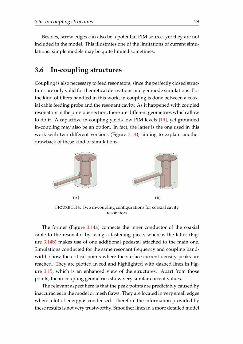
Coupling is also necessary to feed resonators, since the perfectly closed struc-tures are only valid for theoretical derivations or eigenmode simulations. Forthe kind of filters handled in this work, in-coupling is done between a coax-ial cable feeding probe and the resonant cavity. As it happened with coupledresonators in the previous section, there are different geometries which allowto do it. A capacitive in-coupling yields low PIM levels [19], yet groundedin-coupling may also be an option. In fact, the latter is the one used in thiswork with two different versions (Figure 3.14), aiming to explain anotherdrawback of these kind of simulations.
(A) (B)
FIGURE 3.14: Two in-coupling configurations for coaxial cavityresonators
The former (Figure 3.14a) connects the inner conductor of the coaxialcable to the resonator by using a fastening piece, whereas the latter (Fig-ure 3.14b) makes use of one additional pedestal attached to the main one.Simulations conducted for the same resonant frequency and coupling band-width show the critical points where the surface current density peaks arereached. They are plotted in red and highlighted with dashed lines in Fig-ure 3.15, which is an enhanced view of the structures. Apart from thosepoints, the in-coupling geometries show very similar current values.
The relevant aspect here is that the peak points are predictably caused byinaccuracies in the model or mesh flaws. They are located in very small edgeswhere a lot of energy is condensed. Therefore the information provided bythese results is not very trustworthy. Smoother lines in a more detailed model

30 Chapter 3. Current Analysis in Coaxial Resonators
(A)(B)
FIGURE 3.15: Current density peaks for in-coupling configura-tions from Figure 3.14
or further mesh refinements would be a possible approach, yet the computa-tional cost exceeds dramatically the usefulness of the results.
3.7 Conclusions
As it was stated in the objectives of the Thesis, one of the goals was to studyhow geometry variations could mean a change in current values and there-fore enhance or deteriorate interference levels. Such information may beused to perform a PIM-aware optimization process or to decide which partsshould be handled more carefully at the manufacturing stage.
The starting point to do so has been the coaxial cavity resonator, obtain-ing the maximum surface current density values for several geometries. Allof them are equivalent in terms of resonant frequency and outer dimensions,but not in the inner structure. Some interesting results have helped to pro-pose a more innovative variation from the original resonator.
Besides, two more complex situations - coupled resonators and in-couplingstructures - have been analysed. They have helped to highlight the limita-tions of this kind of studies regarding PIM.
Some main ideas can be concluded from this Chapter. In first place, cur-rent density values do not directly give information about PIM levels, yetthey help finding the areas where interference could be enhanced in pres-ence of a PIM source.
Besides, in coaxial cavity resonators, the radius is the parameter with thebiggest impact in current density values. Structures tending to bigger radiuswould be better to avoid PIM. That should be kept in mind when optimizingfilters or deciding where to place connections or junctions.

3.7. Conclusions 31
Finally, concerning model limitations, the simplicity is one of the mainhandicaps to obtain relevant results to relate with interference levels. Be-sides, insights derived from practical experience are always worth consider-ing, especially in a heuristic issue as PIM. Other aspects such as the meshquality may have an impact in the reliability of results. At a certain point, itis important to evaluate if the computational cost overcomes the usefulnessof the simulation results.

33
Chapter 4
Circuital Model of PIM Sources
4.1 Motivation
Finding the source behind high PIM levels has been one of the most commonapproaches to deal with this issue, as it has been presented in Chapter 2.That has proven to be hard and costly in terms of resources, specially consid-ering that PIM is subject to a low repeatability. However, PIM models maybe proposed to try to analyse the consequences of the undesired interferencesregardless of the origin, and that is the scope of this and the following chap-ter.
Unlike Chapter 3, this one offers a circuital perspective of PIM in mi-crowave filters instead of focusing in the three-dimensional structure. Thelimited insight provided by current simulations and the need of handlingbigger and more complex devices makes it natural to take a different ap-proach. Since the goal of this work is to focus on PIM at the design stage, itis also reasonable to try to introduce it in the earlier stages of filter synthesisand design.
Of course, it is not possible to predict or simulate PIM values withoutknowing the source, yet it may be feasible to compare the effects of the samesource when it is moved around the filter. In this case, the same source meansthat the non-linear coefficients causing the intermodulation remain constantthroughout the process. Consequently, the most sensitive topological areasmay be detected. Design decisions such as the filter topology may be influ-enced by such information.
The advantage of dealing with circuits is double. On one hand, compu-tational and time costs are very low. On the other hand, a circuital model ismuch easier to modify and attach to previously existing designs.
Keysight Genesys [34] has been the software used for the study presentedhere, in particular the Harbec (Harmonic Balance) simulation module [35].

34 Chapter 4. Circuital Model of PIM Sources
4.2 PIM source models
The first question which arises when thinking about IM products is how toproperly introduce non-linearities in a circuit. Either the existing compo-nents must be made non-linear or new elements must be added. Besides, itmay also be discussed whether the PIM frequency can be intrinsically gener-ated inside the circuit or added as an external source. Instead of presentingdirectly the final model, four possibilities are briefly described and schemati-cally depicted in Figure 4.1. The reasons why almost all of them are discardedare also stated.
(A) (B)
(C) (D)
FIGURE 4.1: Four different ideas to include a PIM source in alinear circuit. f1 and f2 belong to the passband.
1. Oscillator at PIM frequency - Figure 4.1aAn extra source is included directly at the IM3 frequency ( fPIM and theresponse of the filter is analysed. Such approach is a very simple andlimited. It does not represent the interaction between tones which is thebasis of intermodulation.
2. Oscillator at a frequency in the filter passband - Figure 4.1bAn extra source is included in a different part of the circuit at a fre-quency within the passband ( f2) so that IM products are created. Twoproblems arise here. Firstly, addition of extra sources inside the circuitcauses a matching issue that disturbs the normal filter response. Be-sides, the tones interacting to create PIM ( f1, f2) should both come fromthe filter input, therefore this model does not describe reality either.

4.2. PIM source models 35
3. External non-linear element, e.g. diode - Figure 4.1cA non-linear element with a known and controlled response is included.An auxiliary frequency ( fx) is used to generate the wanted IM products.The whole circuit is made non-linear and therefore the IM frequenciesare generated. Matching issues should be handled as well.
4. Internal non-linear element - Figure 4.1dThe response of one of the linear elements in the circuit is modified sothat non-linear terms are included. IM frequencies are consequentlygenerated.
The first two options are far from representing a PIM source in a passivecircuit, therefore they are discarded. The other two, i.e. the external andinternal elements, are discussed a bit more in detail, although by taking alook at Figure 4.1 it is clear that the internal non-linear element seems to be amore trustworthy model.
4.2.1 External non-linear element as a PIM source
Adding the non-linearity thanks to a new element, for instance a diode, re-quires both another source and an isolation element to keep the linear re-sponse of the filter unchanged. Consequently, the PIM source would looklike the subcircuit in Figure 4.2. It could be then placed in different positionsaround the circuit, for instance in series or parallel with the resonators.
FIGURE 4.2: Circuital PIM source model with diode
The three parameters of the PIM source would be the power and fre-quency of the oscillator and the resistor. The latter should be extremely high,because it is the way to isolate the linear filter response. The oscillator poweris related to the PIM level measured at the filter output and it would be themain parameter to be adjusted. Finally, the oscillator frequency would beone that mixed with the input tone would cause an IM product at the knownPIM frequency.

36 Chapter 4. Circuital Model of PIM Sources
This first model presents many limitations. Firstly and most important,IM products should be created when two input tones in the passband inter-act, therefore no auxiliary frequency or source should be used. In that way,the model does not represent what is happening. Besides, the use of the re-sistor to isolate the filter is not an accurate procedure.
4.2.2 Internal non-linear element as a PIM source
This last option is probably the most logical one as well, yet it was importantto highlight whether other ideas were feasible and the reasons to not to usethem.
In this case, the idea is to make one of the resonator elements directlynon-linear, either the capacitor, the inductor or the resistor. Then, two inputtones at frequencies within the passband would be enough to generate IMproducts. The linear coefficient would be maintained, therefore the basicfilter response would remain the same.
The main advantage of this procedure is that it does not require any ad-ditional elements. It also depicts what happens in real life, since the onlysource is the one at the filter input and any other frequency is caused by thenon-linearity. Besides, the use of coefficients to adjust the behaviour of thePIM source is quite intuitive.
As a result, the model explained in detail in the following section consistson a non-linear inductor (NLI) as IM generator. A non-linear resistor wasinitially discarded aiming to include the non-linearity in one of the intrinsicelements of an ideal resonator. Then, due to the strong relation between PIMand current, the inductor was the chosen element. Some tests were also con-ducted with a non-linear capacitor instead, yet the results were not reliable.
4.3 Non-Linear Inductor (NLI) as a PIM source
A non-linear inductor is available in one of the Genesys libraries (Figure 4.3).Several different responses are possible, for instance polynomial or exponen-tial. Following a simple Taylor expansion, the polynomial response is cho-sen. Therefore, the inductance of the NLI will depend on the current passingthrough it according to:
L(i) = l0 + l1 · i + l2 · i2 + l3 · i3...

4.3. Non-Linear Inductor (NLI) as a PIM source 37
The next step is to determine the number of relevant coefficients for thePIM study, together with their value. In order to do so, the output voltagecaused by two input tones at different frequencies is theoretically obtained.The frequencies of interest are the ones corresponding to IM3 products.
FIGURE 4.3: Genesys model of a non-linear inductor (NLI)
4.3.1 IM products with NLI
Given a NLI (Figure 4.3) with a current-dependent inductance L(I):
L(i) = l0 + l1 · i + l2 · i2
and two input tones with frequencies f1 and f2 which can be written as:
i(t) = A1sin(ω1t) + A2sin(ω2t)
The voltage across a non-linear inductor can be expressed as [36]:
v(t) = L(i) · di(t)dt
The IM products can be obtained as follows:
v(t) = (l0 + l1 · i(t) + l2 · i(t)2) · di(t)dt
=
= [l0 + l1(A1sin(ω1t) + A2sin(ω2t)) + l2(A1sin(ω1t) + A2sin(ω2t))2]·
[ω1A1cos(ω1t) + ω2A2cos(ω2t)]
Expanding the expression:
v(t) = lo · [ω1A1cos(ω1t) + ω2A2cos(ω2t)]+
+l1 · [ω1A21sin(ω1t)cos(ω1t) + ω1A1A2sin(ω2t)cos(ω1t)+
+ω2A1A2sin(ω1t)cos(ω2t) + ω2A22sin(ω2t)cos(ω2t)]+
+l2 · [A21sin(ω1t) + 2A1A2sin(ω1t)sin(ω2t) + A2
2sin(ω2t)]·
·[ω1A1cos(ω1t) + ω2A2cos(ω2t)]

38 Chapter 4. Circuital Model of PIM Sources
Using trigonometric identities and grouping terms, the IM products andtheir amplitudes are:
ω1 · [l0A1 + l2 · (14 A3
1 +12 A1A2
2)] cos(ω1t)ω2 · [l0A2 + l2 · (1
4 A32 +
12 A2A2
1)] cos(ω2t)l1
ω12 A2
1 sin(2ω1t)l1
ω22 A2
2 sin(2ω2t)−l2
ω14 A3
1 cos(3ω1t)−l2 ω2
4 A32 cos(3ω1t)
l1A1 A2
2 (ω1 −ω2) sin((ω2 −ω1)t) IM2
l1A1 A2
2 (ω1 + ω2) sin((ω1 + ω2)t) IM2
l2A1 A2
22 (ω2 − ω1
2 ) cos((2ω2 −ω1)t) IM3
−l2A1 A2
22 (ω2 +
ω12 ) cos((2ω2 + ω1)t) IM3
l2A2
1 A22 (ω1 − ω2
2 ) cos((2ω1 −ω2)t) IM3
−l2A2
1 A22 (ω1 +
ω22 ) cos((2ω1 + ω2)t) IM3
The derivations show both the input frequencies, the higher harmonicsand the IM products of second and third order. It is clear that coefficient l2controls IM3 products, which are the most dangerous and the ones analysedfor PIM measurements. Besides, from now on the NLI will have l0 set to thenominal linear value and l1 set to zero, since the second order IM productsare not interesting from a PIM perspective.
4.3.2 NLI coefficient determination
Considering the previous derivations, coefficient l2 must be determined tohave the PIM source model ready to use. It is important to remember that itis a parameter in the model with no direct connection with a physical dimen-sion. Consequently, it will not give information about absolute PIM levelsand it is not extremely important to set a very accurate value for l2, as longas it remains the same in all simulations.
However, a good approach to set a value for the coefficient is to considerthe order of magnitude of manufactured PIM sources [37]: -110 dBm mea-sured at IM3 frequency for two input tones of 43 dBm. Running a simulationof the circuit which appears in Figure 4.4, l2 is set to 3.5e-16 to obtain thedesired level at the so-called PIM frequency. That value is small, which cor-responds with the idea of a very weak non-linear behaviour.

4.4. Placement of PIM sources at filtering networks 39
FIGURE 4.4: PIM source measurement simulation setup
4.4 Placement of PIM sources at filtering networks
Now that the PIM source has been modelled, the next step is to analyse thedifferent ways to include it in a filter like the ones presented in Chapter 2.The main two positions to consider are either in the resonators themselves ornext to the inverters, modelling a non-linearity in the couplings. These twooptions appear in Figure 4.5.
(A) PIM source in the resonator
(B) PIM source in the coupling
FIGURE 4.5: Possible locations of PIM sources in a filter
The former (Figure 4.5a) emulates any kind of non-linearity at the reso-nant cavity. For instance, a tuning screw, a bad contact between the cylinderand the top hat or material shavings. On the contrary, the latter (Figure 4.5b)represents non-linear issues in the coupling between cavities. In this case, ofcourse, the coefficient l0 of the NLI is also set to zero. However, the maindisadvantage of this set-up is how unspecific it is. For example, it is difficultto decide if a non-linearity in the coupling should be represented by placingthe NLI before or after the resonator in the circuital model, specially whendealing with complex designs.

40 Chapter 4. Circuital Model of PIM Sources
As a result, the filters analysed in the following chapter have the NLIincluded always at the resonator.
4.5 Conclusions
This chapter aimed to establish the basic PIM model to include in the filtersin the last part of this work. Since the circuital approach consists in defininga PIM source, i.e. a non-linearity, and move it around the circuit, it was worthexplaining in detail how the model is built.
Firstly, different ideas are discussed to keep the most simple and reason-able approach: include the non-linearity in one of the previously existingfilter elements. In particular, an inductor with a polynomial response is theone considered in this work, mainly because of the relation between PIM andcurrent.
Then, the important terms of the polynomial must be identified. The the-oretical derivations confirm that the coefficient of the quadratic term, l2, isthe one generating and controlling the level of the third-order IM products.These are the most relevant ones in a PIM study.
The absolute value of the non-linear coefficient is not extremely relevant,since subsequent simulations intend to compare how PIM levels vary, in-stead of reading exact values. However, a sensible approach to choose atleast the order of magnitude may be to evaluate the NLI as commercial PIMreferences.
Finally, the NLI must be placed in the filter network. Seeking for simplic-ity, it will always be part of the resonator, as if the non-linearity was anythinghappening at the resonant cavity in the real device.
Now that the model is set, it is imperative to simulate it in different filterdesigns. The goal is double. On one hand, to see if the results are reasonableand correspond with real experience, taking into account everything knownabout PIM. On the other hand, to evaluate the response of PIM levels whenthe NLI is moved from one resonator to another, aiming to obtain any designadvice.

41
Chapter 5
Circuital Analysis of Filters withPIM sources
5.1 Motivation
In the previous chapter, a PIM source model has been established so that itis easy to introduce in a bigger circuit. When placed in filters, simulationsshould give results coherent with what is known about PIM. Depending onthe obtained results, it will be possible to validate the model and keep usingit in more complex structures, for example diplexers or combiners.
Apart from that validation, interesting insight from a design perspectivemay also be obtained. As it was explained in Chapter 2, different topolo-gies are available to implement the same response. Knowing which partsof the filter are more sensitive to PIM sources, a better choice may be made.Essentially, it is the same idea behind the current analysis in cavities (Chap-ter 3), yet at an earlier stage. Before, it implied geometrical variations inthree-dimensional structures, but now it is related to cross-coupling posi-tions, for instance.
In the current chapter, the PIM source model is introduced in differentkinds of filters. All-pole responses are considered in first place, before mov-ing to more sophisticated filters, with one transmission zero. The NLI ismoved around all filter resonators in each case, to see how PIM levels fluctu-ate.
Finally, a diplexer with dual filters is studied in detail, as an example ofhow this model could be used to analyse PIM behaviour in real designs.
All filter synthesis has been made with own scripts in Matlab [38], whereasGenesys has been used for the simulations, in particular the Harbec module[35].

42 Chapter 5. Circuital Analysis of Filters with PIM sources
5.2 Analysis setup and considerations
When the PIM issue was stated for the first time in Chapter 1, two commonsituations within the mobile communications field were shown. Figures areincluded here again for the sake of clarity. (Figure 5.1), with the most relevantPIM (transmitted or reflected) in each case.
(A) Transmitted PIM (B) Reflected PIM
FIGURE 5.1: Examples of PIM scenarios in mobile communica-tions filter applications
In this chapter, the two different PIM situations are analysed. TransmittedPIM is measured at the output of the structures (ANT port, P2), whereas re-flected PIM is measured at the physical input (P1), although it may representthe filter output. Firstly, PIM frequencies can be divided into in-band or out-band PIM. Such classification reflects whether the IM3 product - the only oneaddressed in this work - lands within the filter passband or not. In the firstarchitecture (Figure 5.1a), TX and RX filters are completely different struc-tures, therefore generated PIM lands outside the TX filter passband: out-bandPIM is interesting.
On the contrary, both TX and RX bands belong to the same structure inthe second architecture (Figure 5.1b). As a result, IM3 products land in thefilter passband (in-band PIM), although in a different part of it.
Consequently, the analysis involves the simulation of PIM levels both in-and out-band, starting with the simplest all-pole filters. For all single filter-ing structures, the analysed scenario will correspond to the situation in Fig-ure 5.1, i.e. transmitted PIM will be measured considering the filter as theTX one. Apart from sophisticated responses such as transmission zeros, theimpact of aspects like the filter bandwidth will also be considered.

5.2. Analysis setup and considerations 43
Afterwards, reflected PIM will be introduced through the analysis of twodual filters like the one in Figure 5.1b.
Finally, before going in detail to the filters themselves, it may be relevantto explain the kind of plots shown in this chapter to evaluate PIM levels.They are very similar to the one in Figure 5.2.
FIGURE 5.2: Explanation of the typical PIM plots included inthis work
The graph represents the output power of the IM3 product (transmittedPIM) when the input tones are moved along the filter passband (1805 - 1880MHz) when one resonator has the NLI. If that is a TX filter, IM3 is only rele-vant at RX band, yet all frequencies are plotted here for the sake of general-ization.
To sweep the input tones, one of them is always fixed at the lowest fre-quency ( f1=1805 MHz) whereas the other moves along the rest of the pass-band ( f2=1806 - 1880 MHz). Consequently, two kinds of third-order IM prod-ucts appear: one at the right side of the input tones (2 f2 − f1) and one at theleft side (2 f1− f2). The areas are highlighted in green in Figure 5.2. The latteris the one landing at RX band, since it is often located at lower frequencies.
Of course, the frequency sweep can be done the other way around: leav-ing f2 or any other frequency fixed and varying f1.
Finally, the NLI is the same as in Chapter 4, except for the coefficient valuel2. In these simulations, l2=1e-20.
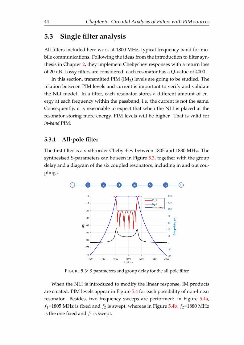
44 Chapter 5. Circuital Analysis of Filters with PIM sources
5.3 Single filter analysis
All filters included here work at 1800 MHz, typical frequency band for mo-bile communications. Following the ideas from the introduction to filter syn-thesis in Chapter 2, they implement Chebychev responses with a return lossof 20 dB. Lossy filters are considered: each resonator has a Q-value of 4000.
In this section, transmitted PIM (IM3) levels are going to be studied. Therelation between PIM levels and current is important to verify and validatethe NLI model. In a filter, each resonator stores a different amount of en-ergy at each frequency within the passband, i.e. the current is not the same.Consequently, it is reasonable to expect that when the NLI is placed at theresonator storing more energy, PIM levels will be higher. That is valid forin-band PIM.
5.3.1 All-pole filter
The first filter is a sixth-order Chebychev between 1805 and 1880 MHz. Thesynthesised S-parameters can be seen in Figure 5.3, together with the groupdelay and a diagram of the six coupled resonators, including in and out cou-plings.
FIGURE 5.3: S-parameters and group delay for the all-pole filter
When the NLI is introduced to modify the linear response, IM productsare created. PIM levels appear in Figure 5.4 for each possibility of non-linearresonator. Besides, two frequency sweeps are performed: in Figure 5.4a,f1=1805 MHz is fixed and f2 is swept, whereas in Figure 5.4b, f2=1880 MHzis the one fixed and f1 is swept.
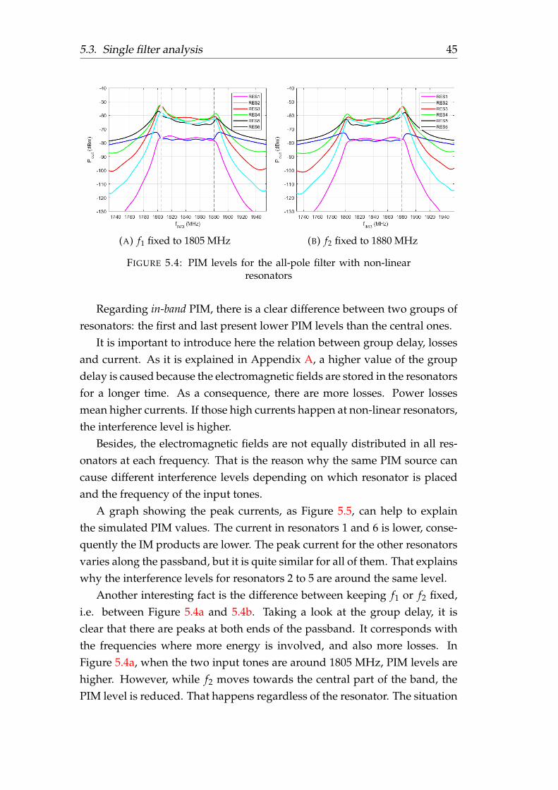
5.3. Single filter analysis 45
(A) f1 fixed to 1805 MHz (B) f2 fixed to 1880 MHz
FIGURE 5.4: PIM levels for the all-pole filter with non-linearresonators
Regarding in-band PIM, there is a clear difference between two groups ofresonators: the first and last present lower PIM levels than the central ones.
It is important to introduce here the relation between group delay, lossesand current. As it is explained in Appendix A, a higher value of the groupdelay is caused because the electromagnetic fields are stored in the resonatorsfor a longer time. As a consequence, there are more losses. Power lossesmean higher currents. If those high currents happen at non-linear resonators,the interference level is higher.
Besides, the electromagnetic fields are not equally distributed in all res-onators at each frequency. That is the reason why the same PIM source cancause different interference levels depending on which resonator is placedand the frequency of the input tones.
A graph showing the peak currents, as Figure 5.5, can help to explainthe simulated PIM values. The current in resonators 1 and 6 is lower, conse-quently the IM products are lower. The peak current for the other resonatorsvaries along the passband, but it is quite similar for all of them. That explainswhy the interference levels for resonators 2 to 5 are around the same level.
Another interesting fact is the difference between keeping f1 or f2 fixed,i.e. between Figure 5.4a and 5.4b. Taking a look at the group delay, it isclear that there are peaks at both ends of the passband. It corresponds withthe frequencies where more energy is involved, and also more losses. InFigure 5.4a, when the two input tones are around 1805 MHz, PIM levels arehigher. However, while f2 moves towards the central part of the band, thePIM level is reduced. That happens regardless of the resonator. The situation

46 Chapter 5. Circuital Analysis of Filters with PIM sources
FIGURE 5.5: Peak current at the resonators
is just the opposite in Figure 5.4a: higher PIM values are reached when thetwo tones are around 1880 MHz, since f2 is always fixed.
Finally, the out-band PIM also follows the expected behaviour. Since PIMis measured at the filter output, the closer the NLI is to the output, the higherthe measured power. That happens in both Figure 5.4a and 5.4b, for frequen-cies at the right and left side of the passband. However, there is one excep-tion: resonator 5 always presents the highest PIM value, even more than thesituation when resonator 6 has the non-linearity.
5.3.2 Filters with one transmission zero
When facing demanding electrical responses, it is very common to make useof transmission zeros (TZ) to achieve higher rejection closer to the passband.In this work, a sixth-order Chebychev filter with one TZ is analysed (6-1).The filter characteristics are the same in terms of frequency band (1805-1880MHz), return loss (20 dB) and Q (4000).
Positive cross-coupling
Firstly, a TZ is included at the right side of the passband, i.e. above. Thatimplies a positive cross-coupling between two resonators, which creates atransmission zero at 1900 MHz. The synthesized response appears in Fig-ure 5.6, together with the group delay. It is clearly seen that higher rejectioninvolves higher group delay.
The previous response can be implemented by using six different topolo-gies, depending on where the cross-coupling is placed. They have beennamed from A to F, and they appear as diagrams in Figure 5.7. In eachcase, the resonant frequency of the resonators and the coupling values are

5.3. Single filter analysis 47
FIGURE 5.6: S-parameters and group delay for the 6-1 filterwith positive cross-coupling
different. In general, the resonator under the coupling resonates at a higherfrequency than the others.
FIGURE 5.7: Six different topologies to implement the responsein Figure 5.7
Each resonator in each topology can be made non-linear to check the IMlevels. Topologies A-F, B-E and C-D are symmetric, yet the PIM analysiswill not be so. However, It is not necessary to include the 36 simulations toexplain the main ideas. Only PIM levels measured for topologies A,B and Cwhen the frequencies f1 and f2 are fixed. They appear in Figure 5.8.

48 Chapter 5. Circuital Analysis of Filters with PIM sources
(A) Topology A, f1 fixed to 1805 MHz (B) Topology A, f2 fixed to 1880 MHz
(C) Topology B, f1 fixed to 1805 MHz (D) Topology B, f2 fixed to 1880 MHz
(E) Topology C, f1 fixed to 1805 MHz (F) Topology C, f2 fixed to 1880 MHz
FIGURE 5.8: PIM levels measured at the output (L) for the 6-1filter with positive cross-coupling

5.3. Single filter analysis 49
Regarding in-band PIM, some conclusions can be obtained:
• Resonators 1 and 6 present the lowest PIM levels, as long as they arenot jumped by the cross coupling (topology A).
• The resonator jumped by the cross coupling (1 in A, 2 in B, 3 in C)generates almost the lowest PIM at the lower part of the passband -where it stores less energy -. On the contrary, interference values aremaximal when the input tones are at the higher part of the passband -where the resonator stores more energy-.
• PIM values for the other resonators are quite stable and similar in thecentral part of the passband regardless of the topology.
Figure 5.9 helps to verify the behaviour of the jumped-by resonators. Itis clear how the current increases when moving towards higher frequencies.Besides, its maximum value increases as well.
FIGURE 5.9: Peak current in jumped resonators for topologiesA,B and C
Regarding out-band PIM, other ideas are also worth highlighting:
• When the non-linearity appears before the cross coupling, the transmis-sion zero can also be seen at the PIM values, e.g. resonators 1 and 2 intopology C.
• As it happened in all-pole filters, the closer to the output, the higher thetransmitted PIM value, except for resonators 5 and 6. The highest PIMlevel is achieved when the NLI is placed at resonator 5.

50 Chapter 5. Circuital Analysis of Filters with PIM sources
Negative cross-coupling
The same analysis can be performed when the TZ is introduced at the otherside of the passband, i.e. the cross-coupling is negative. Once more, the filtercharacteristics are the same except for the TZ, which is placed at 1765 MHz.The S-parameters and the group delay appear in Figure 5.10.
FIGURE 5.10: S-parameters and group delay for the 6-1 filterwith negative cross-coupling
(A) Topology D, f1 fixed to 1805 MHz (B) Topology D, f2 fixed to 1880 MHz
FIGURE 5.11: PIM level for the 6-1 filter with negative coupling
All topologies from Figure 5.7 can be used to implement the response.However, only one of them is included here for the sake of concision: topol-ogy D. The obtained PIM levels appear in Figure 5.11 for both frequency

5.3. Single filter analysis 51
sweeps: when f1 or f2 are fixed. With negative couplings, the jumped-byresonator has a lower resonant frequency than the others.
The plots confirm the conclusions highlighted for the 6-1 filter with posi-tive coupling. Yet now everything that happened at higher frequencies takesplace at the lower part of the spectrum and vice versa.
It is interesting to notice that resonator 5 keeps being the one causinghigher out-band PIM levels.The only situation where that does not happen isin topology E, when it is the one jumped by (Figure 5.11). Even in that case,its level is not very low, but equal to the one caused by other resonators.
Other variations: bandwidth
The influence of the filter bandwidth may be a relevant feature to consider aswell. In order to do so, another 6-1 filter with positive coupling is designed.
FIGURE 5.12: S-parameters and group delay for the 6-1 filterwith positive coupling and double bandwidth
The central frequency is the same, yet the passband goes from 1767.5 to1917.5 MHz, which means a bandwidth twice as big as the one from Fig-ure 5.6. The response can be seen in Figure 5.12, together with the groupdelay. Besides, topology D from Figure 5.7 is chosen.
When PIM levels are compared with the original filter with the sametopology (Figure 5.13), one important aspect should be highlighted: IM levelis around 10 dB lower in the wider filter. It can be concluded that narrowresponses lead to greater PIM values due to higher group delay and storedenergy.

52 Chapter 5. Circuital Analysis of Filters with PIM sources
(A) Original filter, BW=75 MHz (B) Double bandwidth, BW=150 MHz
FIGURE 5.13: Comparison of PIM levels for 6-1 filters with pos-itive coupling and different bandwidth (75 vs 150MHz)
5.4 Example: complex structures and reflected PIM
After studying the response of filters when PIM sources are included, theflexibility of the model allows to move up to more complex structures. Inthis section, one diplexer like the one in Figure 5.14 will be analysed in detail.The main goal is to find the relevant frequencies to look at in terms of PIM.Besides, it allows to introduce reflected PIM, since only transmitted PIM hasbeen handled so far.
FIGURE 5.14: Diagram of the diplexer
There are two dual filters in Figure 5.14, and a diagram of the frequencybands can be seen in Figure 5.15. The first filter works from 1710 to 1880

5.4. Example: complex structures and reflected PIM 53
MHz, but that includes both transmission and reception bands. On the con-trary, the second filter has its passband between 1920 and 2170 MHz, includ-ing two sub-bands as well. The common port of the structure is the outputof the TX filters and the input of RX filters simultaneously.
FIGURE 5.15: Frequency bands of the diplexer
PIM issues are caused by the TX bands. For filter 1, it must be verified ifinput TX tones would cause IM3 at RX bands of filter 1 itself (in-band PIM)or filter 2 (out-band PIM). In-band PIM should be measured at the output ofthe RX filter, i.e. the input of the structure, therefore it is reflected PIM. Out-band PIM can be measured at the input of the RX filter, i.e. the common port,because filter 2 just increases the attenuation level. PIM relations are exactlythe same for filter 2.
Filters should be handled separately and then combined together.
Filter 1
Filter 1 has the same characteristics as the other presented in this chapter:sixth-order Chebychev, 20 dB return loss, Q value of 4000. One TZ is includedat 1905 MHz. Its response appears in Figure 5.16, together with a diagram ofthe topology.

54 Chapter 5. Circuital Analysis of Filters with PIM sources
FIGURE 5.16: S-parameters of Filter 1
The filter passband includes both TX and RX band, as it can be seen in Fig-ure 5.17. Besides, two input tones from the TX sub-band create IM3 productsat the two RX bands, like it was expected.
FIGURE 5.17: Frequency spectrum for filter 1
The IM3 out-band product can be measured like it has previously done inthis chapter: at the filter output. However, the IM3 in-band signal requiresto measure the reflected power at the filter input. In order to do that, anideal coupler has been used, with no coupling relation, perfect isolation andno insertion losses. Thanks to it, the results that appear in Figure 5.18 wereobtained.
As it was previously done, one of the input tones was fixed ( f1 to 1805MHz) and the other was swept within the TX band. Power levels at frequen-cies higher than 1800 MHz correspond to transmitted PIM. The relevant partis beyond the dashed blue line, which marks the beginning of the RX bandof filter 2. The curves at lower frequencies (below 1800 MHz) correspond toreflected PIM.

5.4. Example: complex structures and reflected PIM 55
FIGURE 5.18: PIM values for filter 1 f1 fixed to 1805 MHz
The behaviour of out-band PIM corresponds to the analysis done in previ-ous sections. For reflected PIM, levels are lower, yet they follow the conclu-sions derived for in-band PIM. Besides, the levels are quite similar regardlessof which resonator holds the non-linearity.
Filter 2
Filter 2 presents the same characteristics in terms of order, return loss or Qvalue. Moreover, there is a TZ at 1885 MHz. The filter response appears inFigure 5.19.
FIGURE 5.19: S-parameters of Filter 2

56 Chapter 5. Circuital Analysis of Filters with PIM sources
TX and RX sub-bands are more spaced than in filter 1, therefore the band-width is wider. It causes that two input tones from the TX band do not causeany IM3 products that land in the RX bands. Consequently, the analysis offilter 2 as a single device is done.
Diplexer
Diplexing techniques are a wide field of study themselves [32], but for thisexample it is just enough to adjust the circuital model. Figures 5.20 and 5.21show a diagram of the whole diplexer and the Genesys schematic respec-tively. Joining the filters together requires the use of an extra cavity andcouplings to match the common port (P3). Besides, there must be two idealdirectional couplers at the filter inputs (P1, P2) to be able to measure PIM atthe input (P4, P5).
FIGURE 5.20: Diagram of the diplexer including the directionalcouplers and port naming
FIGURE 5.21: Genesys schematic for the diplexer
When the two filters are joined together, it can be considered the situationof input tones in both TX bands simultaneously. If the input tones are at the

5.4. Example: complex structures and reflected PIM 57
two ends of the bands, the spectral situation would be as the one plotted inFigure 5.22. Four different IM products appear:
• IM3 at 1730 MHz (= 2 · 1805− 1880 MHz)Third-order IM product from TX1 that lands in RX1 (in-band PIM). Mea-sured at the output of the RX1 filter, i.e. P4 in Figure 5.20 (reflectedPIM).
• IM3 at 1955 MHz (= 2 · 1880− 1805 MHz)Third-order IM product from TX1 that lands in RX2 (out-band PIM).Measured at the output of the RX2 filter, i.e. P5 in Figure 5.20 (trans-mitted PIM).
• IM product at 1745 MHz(= 1805 + 2110− 2170 MHz)IM product from the combination of TX1 and TX2 that lands in RX1.Measured at the ouput of the RX1 filter, i.e. P4 in Figure 5.20.
• IM product at 1940 MHz(= 1880− 2110 + 2170 MHz)IM product from the combination of TX1 and TX2 that lands in RX2.Measured at the ouput of the RX2 filter, i.e. P5 in Figure 5.20.
FIGURE 5.22: Diplexer frequency spectrum when there are in-put tones from both TX filters
Conducted simulations show the PIM levels in Table 5.1 for each of thefour aforementioned frequencies. The NLI can be placed in twelve differentpositions (six resonators in each filter). The second column shows whichresonator has the non-linearity in each case.
From this data, some information can be obtained:
• Highest PIM levels at all frequencies are achieved when the non-linearityis close to the common port (resonators 5 and 6 for both filters).

58 Chapter 5. Circuital Analysis of Filters with PIM sources
TABLE 5.1: Diplexer PIM levels
P (dBm)@ 1740 MHz @ 1955 MHz @ 1745 MHz @ 1940 MHz
Filter 1
R1 -122 -170 -274 -255R2 -110 -150 -241 -280R3 -107 -138 -211 -240R4 -111 -121 -203 -209R5 -110 -124 -165 -176R6 -118 -123 -141 -144
Filter 2
R1 < -300 -270 -232 -211R2 < -300 -246 -205 -148R3 -268 -226 -184 -143R4 -214 -161 -177 -124R5 -176 -143 -145 -112R6 -142 -127 -130 -115
• IM3 products (1730 MHz, 1955 MHz) present higher values when thenon-linearities are placed in filter 1. That is because such IM productsare caused by the input tones in TX1.
• IM3 in-band product (1730 MHz) has higher levels than the out-bandproduct (1955 MHz), since the latter includes the attenuation from filter2.
• IM products at 1745 and 1940 MHz have higher values when the non-linearity is placed at filter 2. That is because TX2 input tones have agreat contribution to the generated signals.
• IM product at 1745 MHz has a lower level than the one at 1940 MHzbecause the former is out-band for filter 2, whereas the latter is in-band.
It is worth highlighting that all IM levels have been stated here, althoughsome of them are extremely low and they would be considered as no PIM inreal life.
An analysis such as the one performed here is important to confirm whichfilters or resonators should be handled with more care, specially when thereare different TX and RX bands involved. There are frequency bands moresensitive to IM products and that is something to be considered.
5.5. Conclusions 59
5.5 Conclusions
This final chapter of the Thesis makes use of the previous work developedwith the PIM source model. The NLI is included in different filtering net-works to see how PIM levels vary depending on where the non-linearity is.On one side, it allows to verify the adequacy of the model. On the other side,it emphasizes the sensitive areas to keep in mind when moving from designto the manufacturing stage.
The filters presented here have an increasing level of complexity. All-pole Chebychev responses are handled first, before including one TZ. In bothcases transmitted PIM is measured. Finally, an example of a complex devicewith several sub-bands and reflected PIM is described step by step. The goalis to set the basis for a procedure to analyse any structure.
Regarding PIM levels in filters, some important points to highlight are:
• For in-band transmitted PIM:
– PIM levels depend on the energy stored at each resonator for eachfrequency, in terms of current passing through. For symmetricstructures, such as all-pole filters, the PIM levels are quite similarin the whole band regardless of the resonator. However, when aTZ is introduced, the variation in the energy distribution is mostlyseen in the resonator jumped by the cross-coupling.
– PIM levels are low when the non-linearity is placed at the first orlast resonator.
– Filters with negative or positive couplings show a symmetric be-haviour. The main variation applies to the jumped-by resonatorand where the interference that it causes is maximal or minimal.
• For out-band transmitted PIM:
– In general, the closer the non-linearity to the filter output, the greaterthe interference level.
– The exception happens when the non-linearity is placed at thenext-to-last resonator. Then PIM levels are the highest.
Besides, narrow filter responses in terms of bandwidth lead to higher PIMvalues.
Finally, the analysis of the diplexer clarifies some ideas as well. Firstly, itis important to analyse each single filter before joining them together. Once

60 Chapter 5. Circuital Analysis of Filters with PIM sources
the whole structure is completed, if both filters are excited simultaneously,new IM products may appear. Besides, the diplexer has shown how complexstructures or topologies involve transmitted and reflected PIM, together within- and out-band interferences.

61
Chapter 6
Conclusion
6.1 Conclusions
Passive Intermodulation is a crucial issue in mobile communications nowa-days, enhanced by the shortage of frequencies and the limitations in power. Itis a kind of distortion caused by unpredictable non-linearities, mostly relatedwith current. Unlike what happens with the distortion from active devicessuch as amplifiers or mixers, PIM cannot be suppressed once it is there, sinceit appears at the output of filtering structures. Therefore it is interesting tostudy how it is generated in filters and how it may affect their performance.
The goal of this Master Thesis is to study and propose practical ways toimprove PIM performance in microwave filters. The work is focused at thedesign stage, consequently all measures regarding careful manufacturing ormaterial selection are not considered.
The main objective is very ambitious, since PIM has been subject to adeep study from many perspectives, as it was summarized in Chapter 2. Thenovelty brought by this work is the practical approach and the active use ofsimulation tools to deal directly with complex filtering structures.
In particular, two main perspectives have been used: current density anal-ysis in resonant cavities and PIM source modelling in filtering networks.Each of them focuses in one unit (resonator or filter) and one part of thedesign stage (circuital model or three-dimensional cavity). The main con-clusions obtained in each case are explained below. Some of them help todiscard previous misconceptions, for instance the influence of the topologyin the interference levels.
To sum up, the work conducted here has allowed to get some small hintsabout how PIM can be handled at the design stage. It has been challenging,because working with such an heuristic issue from a practical perspectivealways is. However, it has also helped to open new working lines whichmay be explored in future projects.

62 Chapter 6. Conclusion
6.1.1 Current analysis in coaxial resonators
The first approach, developed in Chapter 3, involves the basic element offilters: resonators. Besides, it does not consider the lumped element circuitalelement, but directly the three-dimensional cavity. Since PIM generation isrelated with current non-linearities and PIM level with current amplitude, itis interesting to see how variations of the resonator geometry may modifypeak current values. Then, such information can be used to keep possiblePIM sources (screws, weldings... ) away from those places. Besides, low-current geometries may be used to lead optimization processes.
The simulations conducted in this work show that the radius is the pa-rameter with a bigger impact in coaxial cavity resonators. That is due to itsrelation with the resonator inductance. Other modifications, some of themquite innovative were also tried, yet the obtained results were not very rele-vant.
Structures with bigger radius may be used to replace sensitive connec-tions, for instance the disc variation proposed for the junction of the resonatorwith hat.
Finally, these kind of simulations are also quite limited, as it was alsohighlighted. Their main drawbacks go from the simplicity of the models tothe trade off between computational cost and mesh quality. However, theyare a resonable tool to begin with the study of PIM in filtering structures.
6.1.2 Circuital model of PIM sources and analysis of filtering
networks
The second approach is presented in Chapters 4 and 5. It deals with com-plete filtering networks with complex responses including transmission ze-ros. Circuital models are considered, and they are made non-linear throughthe use of an inductor with a current-dependent inductance. The dependenceis modelled by a second-order polynomial, therefore the IM3 products iden-tified as PIM are created. The advantages of the non-linear inductor are theflexibility to add it in existing circuits and also to modify its value and controlthe interference levels.
Chebychev filters with all-pole and 1-TZ responses are analysed, placingthe PIM source at one resonator at a time and comparing the measured PIMvalues. The simulations do not provide valid PIM levels themselves, yet therelevance of the results is the comparison of the relative differences in IM3
depending on the position.

6.2. Future work 63
The difference between transmitted and reflected PIM is also considered,but only the first one is analysed in detail. The latter is introduced in thediplexer example which concludes Chapter 5, aiming to show how the anal-ysis of a more complex network should be done.
Regarding transmitted PIM, some ideas are derived from the filter sim-ulations. For in-band PIM, the interference is lower when the non-linearityis placed at the first or last resonator. On the contrary, the worst case sce-nario happens when the non-linearity is placed in the resonator jumped bythe cross-coupling. It happens regardless of the topology and therefore thatchoice is not influenced by PIM.
For out-band PIM, the main conclusion is that the highest PIM levels hap-pen when the non-linearity is placed at the next-to-last resonator, regardlessof the topology. Apart from that, results follow an intuitive behaviour: thecloser to the filter output, the greater the interference level.
6.2 Future work
There are some issues brought up in this work that would be worth consid-ering in future projects:
• Model refinement of resonant cavitiesOne work line is to develop a more reliable model of resonant cavi-ties, including more geometrical details. Different kinds of materialscould also be used, including some with non-linearities as PIM sourcesin key areas such as screw edges. IM products could be generated andcompared for different kinds of cavities, to move a step beyond currentdensity.
• Experimental determination of l2 coefficient valueAlthough the value of the l2 coefficient of the NLI was not relevantfor this work, it could be worth determining by practical means. Forinstance, artificial PIM sources could be added to PIM-free filters totry to characterize the source experimentally. Then, the results couldbe interpolated and used to model the behaviour of units experiencingreal PIM problems.
• Experimental verification of the obtained resultsThe derived conclusions from the simulations should be verified withmeasurements. Again, artificial PIM sources could be used, so that

64 Chapter 6. Conclusion
the impact of the different topologies or non-linear resonators are con-firmed. This is the most immediate and relevant working line, since aproject regarding PIM, which is an issue of learning through discovery,cannot be complete lacking real data.

65
Appendix A
Introduction to filter design
This section aims to be a short and practical introduction to filter design forreaders not familiar with the subject. The main ideas used for the filters usedin this work are explained, without delving into mathematical derivations orfilter theory. For detailed information, texts such as [32, 33, 39] are recom-mended.
A.1 Filter parameters
There are four different types of filters: low-pass, high-pass, bandpass andbandstop. The low-pass model is the basic one, since frequency transforma-tions allow to obtain all other responses from the former. Besides, a filtercan have several attenuation profiles, e.g. Butterworth, Chebychev, or Cauer.The Chebychev characteristic is extensively used, due to its sharper responsecompared to others, for instance the Butterworth, and the flatness of the pass-band. Its name is because the filter response approximates the analytical be-haviour of the Chebychev polynomials. In this work, bandpass Chebychevfilters are used.
The first step of filter design involves a process like the one depicted inFigure A.1. Specifications include the bandpass, attenuation and losses. Thetype will be Chebychev, and the filter order will be the necessary one to fulfilthe specifications. Insertion losses are not considered yet.
FIGURE A.1: Working flow for filter design
The filter order refers to the number of resonators needed to achieve thedesired response. Stronger couplings require higher-order filter. Besides,

66 Appendix A. Introduction to filter design
higher order filters imply sharper responses, therefore demanding attenua-tion specifications will require a high-order filter as well.
A.2 Low-pass to bandpass transformation
When the filter order is set, a low-pass filter prototype with lumped compo-nents is obtained. An example of fourth order appears in Figure A.2. Elementvalues g0-g5 come from the Chebychev polynomials.
FIGURE A.2: Example of Chebychev low-pass prototype, N=4
The next step is to transform the low-pass prototype into a bandpass one.Such transformation implies that each inductor or capacitor will become aresonator. However, if that is directly done, the circuit would not represent afeasible network in real life. There are two main issues to handle:
• Resonators must all be of the same kind.
• Resonators are coupled, and such coupling should be represented inthe circuital model as well.
An auxiliary element is used to overcome these problems: the inverter. Itis used to transform the elements of a circuit and their values without chang-ing the response. It appears as a box in Figure A.3. It allows to use four equalparallel resonators coupled one to the next one and to the source (S) and load(L). The value Jx of each inverter is the value of the coupling.The couplingvalues are calculated through the synthesis process. Higher values mean astronger coupling. Besides, the sign indicates if the coupling is inductive orcapacitive.
FIGURE A.3: Example of Chebychev bandpass filter

A.3. Transmission zeros 67
The network from Figure A.3 may also be schematically represented as inFigure A.4, where each circle represents a resonator and each line is a cou-pling.
FIGURE A.4: Diagram of a Chebychev fourth-order filter
At this point, the circuital synthesis of the filter would be finished and theresponse would look similar to the one in Figure A.5, which goes from 1805to 1880 MHz. Return loss has been set to 25 dB and there are no requirementsregarding attenuation.
FIGURE A.5: S-parameters of a fourth-order Chebychev filter
The next step in the design process would be to replace the lumped res-onators with real transmission lines. However, in order to follow this workit is enough with stopping here, since all circuital simulations are conductedwith filters that look like the one in Figure A.3.
A.3 Transmission zeros
Sometimes, the responses provided by regular Chebychev filters (all-pole re-sponses) are not good enough to meet demanding specifications, specially interms of attenuation. As an example, the previous filter (Figure A.5) can beconsidered. If the rejection at 1775 MHz is required to be greater than 30 dB,one possibility is to introduce a transmission zero (TZ) at that frequency. Thenew response would look like the one in Figure A.6.
However, increasing rejection has some cost. As it can be seen when thetwo filter responses are compared, attenuation has increased a lot at the left

68 Appendix A. Introduction to filter design
FIGURE A.6: S-parameters of a fourth-order Chebychev filterwith one TZ
side, yet the opposite effect happens at the right side. Besides, the filter struc-ture it is more complex.
The idea behind a TZ is to create another path for the energy to travel sothat the signals cancel out at the desired frequency. In a topology such as theone in Figure A.4, there is only one possibility to connect the input with theoutput. However, if an extra coupling is added like in Figure A.7, a differentpath is created and a TZ could happen. The circuit would be like the one inFigure A.8, with one extra coupling between two resonators. As it will bediscussed in Chapter 4, there is no unique position for the cross-coupling.
FIGURE A.7: Diagram of a Chebychev fourth-order filter withone TZ
FIGURE A.8: Chebychev bandpass filter with cross-coupling
Introducing a cross-coupling makes the values of the circuit elementschange. In all-pole filters, all resonators have the same resonant frequency,

A.4. Insertion losses and Q value 69
whereas in this kind of responses each of them has a slightly different reso-nant frequency. Besides, the sign of the cross-coupling indicates whether theTZ is at the right side (positive) or at the left side (negative) of the passband.
A.4 Insertion losses and Q value
So far, the filters designed here are dissipationless. To include losses in res-onators, a resistive element must be added, so that a complete parallel res-onator looks like the one in Figure A.9.
FIGURE A.9: Parallel resonant circuit including losses
Besides, a quality factor Q for any resonance phenomena can be defined,in terms of stored energy and energy loss at the resonant frequency ωr [40].Actually, three different Q factors can be defined, depending on which loss isconsidered: unloalded Q (QU), external Q (QE) and loaded Q (QL). They aredefined as follows:
QU ≡ ωrEnergy stored in the resonator
Power loss in the resonator
∣∣∣∣at ωr
QE ≡ ωrEnergy stored in the resonator
Power loss in the external circuit
∣∣∣∣at ωr
QL ≡ ωrEnergy stored in the resonator
Total power loss
∣∣∣∣at ωr
The unloaded Q measures the quality of the resonant circuit itself: if thevalue is infinite, it means that the circuit has no losses. External Q measuresthe coupling between the resonator and the rest of the circuit, whereas theloaded Q includes all the information. The relationship between them is:
1QL
=1
QE+
1QU

70 Appendix A. Introduction to filter design
A.5 Group delay
The group delay is time it takes for a packet of frequencies to go througha system. It is defined as the derivative of the phase characteristic (φ) withrespect to frequency (ω):
τg =dφ
dω
The group delay characteristic for the filter in Figure A.5 appears in Fig-ure A.10. It is only relevant in the passband of the filter.
FIGURE A.10: Group delay characteristic for the filter in Fig-ure A.10
The group delay introduced by the filter is physically made by keepingthe energy stored at the resonators for a certain time. The fields are stored inthe reactive elements of the circuit. However, keeping the signal at the res-onators causes more losses. Therefore the frequencies where the time delayis highest, correspond with the highest insertion losses. That happens at theedges of the passband.
Besides, the inclusion of transmission zeros also has a cost in terms ofgroup delay. The side of the passband where the TZ is introduced suffers anincrease in the group delay as well. On the contrary, the other side ends upwith lower attenuation but also a lower group delay.

71
References
[1] Svenskarna och internet 2017. Tech. rep. World Internet Institute, 2017.URL: http://www.soi2017.se.
[2] D. Murphy. “2.4 BN smartphone users in 2017”. Mobile Marketing Maga-zine (2017). URL: http://mobilemarketingmagazine.com/24bn-smartphone-users-in-2017-says-emarketer.
[3] P.L. Lui. “Passive intermodulation interference in communication sys-tems”. Electronics & Communication Engineering Journal (1990), pp. 109–117.
[4] D. M. Pozar. Microwave Engineering. Wiley, 2011.
[5] A. Christianson and W. Chappell. “Measurement of ultra low passiveintermodulation with ability to separate current/voltage induced non-linearities”. Microwave Symposium Digest (2009).
[6] F. Hall. A prime on passive intermodulation (PIM). Radio Frequency Sys-tems, 2009.
[7] J. R. Wilkerson et al. “Distributed Passive Intermodulation Distortionon Transmission Lines”. IEEE Transactions on Microwave Theory and Tech-niques 59.5 (May 2011), pp. 1190–1205.
[8] Anritsu. Understanding PIM. 2017. URL: https://www.anritsu.com/en-us/test-measurement/technologies/pim#.
[9] J. Russer et al. “Phenomenological Modeling of Passive Intermodula-tion (PIM) due to Electron Tunneling at Metallic Contacts”. MicrowaveSymposium Digest, 2006. IEEE MTT-S International. 2006.
[10] M. Vladimirescu, R. Kwiatkowski, and K. Engel. Passive Intermodula-tion Distortion in RF Coaxial Electro-Mechanical Switches For Space Appli-cations.
[11] C. Vicente and H. L. Hartnagel. “Passive-Intermodulation Analysis Be-tween Rough Rectangular Waveguide Flanges”. IEEE Trans MicrowaveTheory Tech 53.8 (2005).

72 References
[12] C. Vicente et al. “An Experimental Investigation on Passive Intermodu-lation at Rectangular Waveguide Interfaces”. Microwave Symposium Di-gest, 2006. IEEE MTT-S International. (San Francisco, CA, USA, June 11,2006). 2006.
[13] J. R. Wilkinson. “Passive Intermodulation Distortion in Radio FrequencyCommunication Systems”. PhD thesis. North Carolina State Univer-sity, 2010.
[14] E. Rocas et al. “Passive Intermodulation Due to Self-Heating in PrintedTransmission Lines”. IEEE Trans. Microwave Theory Tech. 59.2 (2011),pp. 311–322.
[15] G. C. Bailey and A. C. Ehrlich. “A study of rf nonlinearities in nickel”.Journal of Applied Physics 50 (1 1979), pp. 453–461.
[16] Y. Wu, W. H. Ku, and J. E. Erickson. “A Study of Nonlinearities and In-termodulation Characteristics of 3-Port Distributed Circulators”. IEEETransactions on Microwave Theory and Techniques 24 (2 1976), pp. 69–77.
[17] B. El Banna. “Passive Intermodulation from Printed Circuit Boards”.MA thesis. Royal Institute of Technology (KTH), 2006.
[18] G. Macchiarella, G. B. Stracca, and L. Miglioli. “Experimental Study ofPassive Intermodulation in Coaxial Cavities for Cellular Base StationsDuplexers”. 34th European Microwave Conference. 2004, pp. 981–984.
[19] G. Macchiarella and A. Sartorio. “Passive Intermodulation in MicrowaveFilters: Experimental Investigation”. WMB-7: MTT-S Workshop on FilterII: Practical Aspects of Microwave Filter Design and Realization. 2005.
[20] A. P. Shitvov et al. “Effects of Geometrical Discontinuities on DistributedPassive Intermodulation in Printed Lines”. IEEE Trans. Microwave The-ory Tech. 58.2 (2010), pp. 356–362.
[21] A. J. Christianson, J. J. Henrie, and W. J. Chappell. “Higher Order In-termodulation Product Measurement of Passive Components”. IEEETrans. Microwave Theory Tech. 56.7 (2008), pp. 1729–1736.
[22] J. J. Henrie, A. J. Christianson, and W. J. Chappell. “Linear-NonlinearInteraction and Passive Intermodulation Distortion”. IEEE Trans. Mi-crowave Theory Tech. 58.5 (2010), pp. 1230–1236.
[23] D.E. Zelenchuk et al. “Discrimination of Passive Intermodulation Sourceson Microstrip Lines”. Proceedings of The International Workshop in Multi-pactor, Corona and Passive Intermodulation. 2008.

References 73
[24] J. Henrie, A. Christianson, and W. J. Chappell. “Prediction of PassiveIntermodulation From Coaxial Connectors in Microwave Networks”.IEEE Trans. Microwave Theory Tech. 56.1 (2007), pp. 209–216.
[25] S. Hienonen. “Studies On Microwave Antennas: Passive Intermodula-tion Distortion In Antenna Structures And Design Of Microstrip An-tenna”. PhD thesis. Helsinki University of Technology, 2005.
[26] D. E. Zelenchuk et al. “Passive Intermodulation in Finite Lengths ofPrinted Microstrip Lines”. IEEE Trans. Microwave Theory Tech. 56.11 (2008),pp. 2426–2434.
[27] M. Ye, Y. He, and H. Zhu. “Empirical Equation for Carrier Power De-pendence of Passive Intermodulation Product”. IEEE International Wire-less Symposium. 2015.
[28] S. Hienonen and A. V. Räisänen. “Effect of load impedance on passiveintermodulation measurements”. Electron. Lett. 40.4 (2004), pp. 245–247.
[29] J. Z. Wilcox and P. Molmud. “Thermal Heating Contribution to Inter-modulation Fields in Coaxial Waveguides”. IEEE Transactions on Com-munications (1976).
[30] A. Shitvov and D. Kozlov. “Nonlinear Characterisation for MicrostripFilters with Low Passive Intermodulation”. Integrated Nonlinear Mi-crowave and Millimetre-wave Circuits Workshop. 2017.
[31] ANSYS-HFSS: High Frequency Simulation Software. URL: http://www.ansys.com/Products/Electronics/ANSYS-HFSS.
[32] G. Matthaei, L. Young, and E.M.T. Jones. Microwave Filters, Impedance-Matching Networks, and Coupling Structures. McGraw-Hill, 1964.
[33] R. E. Collin. Foundations for Microwave Engineering. McGraw-Hill, 1992.
[34] Keysight Technologies. Genesys RF/Microwave Synthesis and SimulationSoftware. URL: https://www.keysight.com/en/pc-1297125/genesys-rf-and-microwave-design-software?cc=GB&lc=eng.
[35] Keysight Technologies. Genesys Harbec. URL: https://www.keysight.com/main/editorial.jspx?cc=GB&lc=eng&ckey=1634935&nid=-
11143.0.00&id=1634935.
[36] S. R. Talluri. “Analysis of Transmission Line Models with Non LinearElements for Opposite Phase and Group Velocities”. PhD thesis. JaypeeUniversity of Information Technology, 2016.

74 References
[37] Rosenberger. Passive Intermodulation Analyzers PIM Test Solutions for allApplications. URL: www.rosenberger.com/0_documents/de/catalogs/ba_communication/COM_PIA_2016_Catalog.pdf.
[38] Mathworks. MATLAB. URL: https://www.mathworks.com/products/matlab.html.
[39] R. J. Cameron, C.M. Kudsia, and R.R. Mansour. Microwave Filters forCommunication Systems: Fundamentals, Design and Applications. Wiley,2007.
[40] P.A. Rizzi. Microwave Engineering: Passive Circuits. Prentice Hall, 1988.

TRITA SCI-GRU 2018:019
www.kth.se