study of the impact of void-defect in 11 kv xlpe cable
TRANSCRIPT
International Journal of Scientific & Engineering Research Volume 11, Issue 11, November-2020 330
ISSN 2229-5518
IJSER © 2020
http://www.ijser.org
Study of the Impact of Void-defect in 11 kV XLPE Cable Insulation
M. Alsharif, I. S. Naser
Abstract— Worldwide, electric power distribution relies on a vast network of MV XLPE cables. This paper investigated the variation nature
of electric field distribution of typical energized underground 11 kV XLE armoured insulted cable containing void-defects using finite
element software. The calculations of electric stress in void-defects based on electric stress of insulation materials are presented with a
consideration of the directions of the electrical field stress in voids. The size and location of void-defect as a function of electric stress are
achieved. The electric stresses of the void-defects vary within their sizes, locations, and direction of the applied electric field. The results
will lead to better understanding of the void-defects in armoured XLPE insulated cable in respect to the void size, location, and x- and y-
electric field direction.
Index Terms—MV XLPE cable, Insulation, Partial discharge, Finite element method, Electric stress, Void-defect, Electrostatics.
—————————— ——————————
1 INTRODUCTION
owadays, the most common types of medium voltage (MV) underground cables in use in electrical distribution systems are the Cross-linked polyethylene (XLPE) ca-
bles. The electric strength of the cable insulation material to withstand failure are the result of many factors such as pres-sure, temperature, voltage waveform, conductor material, presence of impurities and imperfections in the insulating ma-terial, and electrode field configurations. However, the insula-tion may deteriorate due to a combination of factors such as ageing, stress, and manufacturing and/or installation errors [1]. In addition, operational stresses that occur in cable insula-tion such as thermal, mechanical and electrical vary with time and can cause degradation due to the physical and chemical changes in cable properties. The major factors which lead to the breakdown of insulation in solid dielectrics are by intrin-sic, electromechanical/chemical, thermal, treeing/tracking phenomenon’s and the presence of voids [2]. Voids may form in insulating material during the manufacture, installation or operation of the high voltage system [3]. The voids are usually filled with a gaseous or a liquid medium [2]. Thus, the voids have lower electric permittivity and breakdown strength than those of the insulation material in which they present. When the applied voltage across the cable increases, the correspond-ing electric field stress over the void increases as well; because of the low permittivity of the gas, a much higher electric field exists in the void compared to the electric field of surrounding the dielectric. If the electric field of the void exceeds the breakdown strength field and electron generation starts, then
partial discharge (PD) will occur. PD over a period of time
leads to apparatus insulation failure. Also, the void initiates further degradation such as internal treeing, surface and coro-na discharges, leading to complete failure of the cable insula-tion system [4]. The probability of a discharge is dependent on many factors such as the temperature, pressure, shape, po-sition, and size of the void. The electric stress within the void is dependent on its axis of orientation with respect to the ap-plied electric field [5]. The behavior of insulation degradation is not yet well understood and there are, a lot of research ac-tivities are being carried out to get a better understanding of discharge degradation [6].
Since, the void can be the source of electrical discharges, it is important to understand the effect of void defects on the electric field distribution at cable insulations [7]. In this paper armoured XLPE cable model is developed to study the behav-ior of electric field of this cable and to analyze the electric stress of different void-defect sizes at different locations with-in XLPE insulted cable. The resultant electric field components in the x- and y- directions are calculated. Consideration of the void-defect electric stress magnitudes, the directions of high electrical field in void-defect, the location of void-defect, the void-defect size in cable insulation will establish knowledge rules in modelling and analysis of medium voltage equipment and degradation phenomena.
The cable dimensions and characteristics are taken from da-ta of a common single-phase 11 kV armoured XLPE cable [8].
2 ELECTRIC FIELD MODELLING
The electric field modelling of typical energized underground 11kV XLE armoured cable with and without insulation defect using finite element software COMSOL is presented.
Electrostatic application mode solves the following Pois-son’s equation:
V 0 r V (1) Where is the charge density.
The electric field intensity is obtained from the negative gradient scalar potential as:
N
————————————————
M Alsharif is an assistant professor in department of agricultural engi-neering, Sebha University, Libya, PH-00 21871 2632960. E-mail: [email protected]
I. S. Nase is a lecturer in department of physics, Education Faculty, Sebha University, Libya, PH-00 21871 2632960. E-mail: [email protected]
IJSER

International Journal of Scientific & Engineering Research Volume 11, Issue 11, November-2020 331
ISSN 2229-5518
IJSER © 2020
http://www.ijser.org
E V (2)
The electric field distribution within the cable cross-section is solved over one applied voltage cycle where a voltage fre-quency of 50 Hz is assumed. 11 kV applied to the conductor and 0 V applied to the outer sheath. The two-dimensional elec-tric field model is solved for a non-degraded system configu-ration as a base for further analysis. Air-filled voids are intro-duced into the model cable insulation to investigate the void electric field stresses. The magnitude of the void electric stress is calculated by:
E = V / d (3)
Where V is the electrical potential differences across the
void: V =V1-V2
V1 and V2 are depending on the position of the void
dc = depth of the void.
3 VOID SETTING
Since, in practice, the existence of spherical void-defect type in insulation material is common [9], air-void in spherical two-dimensional models have been introduced in the XLPE cable insulation cross-sections. The air-filled void-defect will corre-spond to high, medium, and low electric fields. The voids are located adjacent to a conductor, in the middle of the insula-tion, and near the ground sheath, respectively, as shown in Figure 1. Given the symmetry of the cable arrangement, these positions can be related to similar positions around the rest of the region of the cable.
4 RESULTS
4 RESULTS
4.1 Electric Field Distribution
Figure 2 shows the electric field and equipotential distribution within the cable at the point in the AC cycle where the con-ductor potential is at its maximum value. The electric field decreases gradually over the XLPE insulation from the high level at the conductor surface to minimum level at the ground sheath. The electric field is zero at the conductor and ground sheath. The equipotential lines are close to each other where the electric field intensity is high and vice versa. The equipo-tential field lines are parallel to the ground sheath.
4.2 Electric Field Strength of (x-y) Components of Void-defect Over Specific Locations
The electrical stress across air-filled void defects of size 0.5 mm is measured over a single AC cycle of 20 ms in respect of electric field strength of x-component and y-component. This calculation was repeated for different voltage levels in the sin-gle-phase XLPE cable and for the void locations considered in Figure 2.
In the Chart 1 and the Table 1 the maximum values of the electric field in the void over AC cycle are presented. In void positions inserted into the cable model shown in Fig-ure 1, the magnitudes of x-component and y-component of the electric field have been calculated. The results of the analyses are presented in Table 1 and Chart 1.
As expected, in void positions of 1, 2, and 3, the electrical field is in the direction between the centre of the conductor and the earthed sheath. In respect of y-component magnitude, it is much greater than that of the x-component. The data in Figure 3 demonstrates the symmetry of the data. The results of the analysis are presented in Table and Figure 3. Table pre-sents the maximum normal, x- and y electric field of void-defects in kV/mm of size 0.5 mm in positions 1, 2, and 3 con-sidered in Figure 2. The normal electric stress over all posi-tions is in the range of 3.044 kV/mm to 3.884 kV/mm, the y-electric stress component is in the range of 3.044 kV/mm to 3.882 kV/mm, and the x-electric stress component is in the range of 0.061 kV/mm to 0.62 kV/mm.
The electric field of void-defect of position 1 is high, and it
Fig. 2. The electric field and equipotential distribution through the XLPE cable cross-section within the cable at the point in the AC cycle where the conductor potential is at its maximum value.
Fig. 1 Cross-section view of the XLPE cable on x-y plane with air-filled voids in positions, 1, 2, and 3.
.
IJSER
International Journal of Scientific & Engineering Research Volume 11, Issue 11, November-2020 332
ISSN 2229-5518
IJSER © 2020
http://www.ijser.org
decreases gradually over positions 2 and 3, respectively. The electric field magnitude in the position of the void-defect close or around the conductor position 1 is high. The lowest level of electric field is in the position of the void-defect far away from conductor positions 2 and 3.
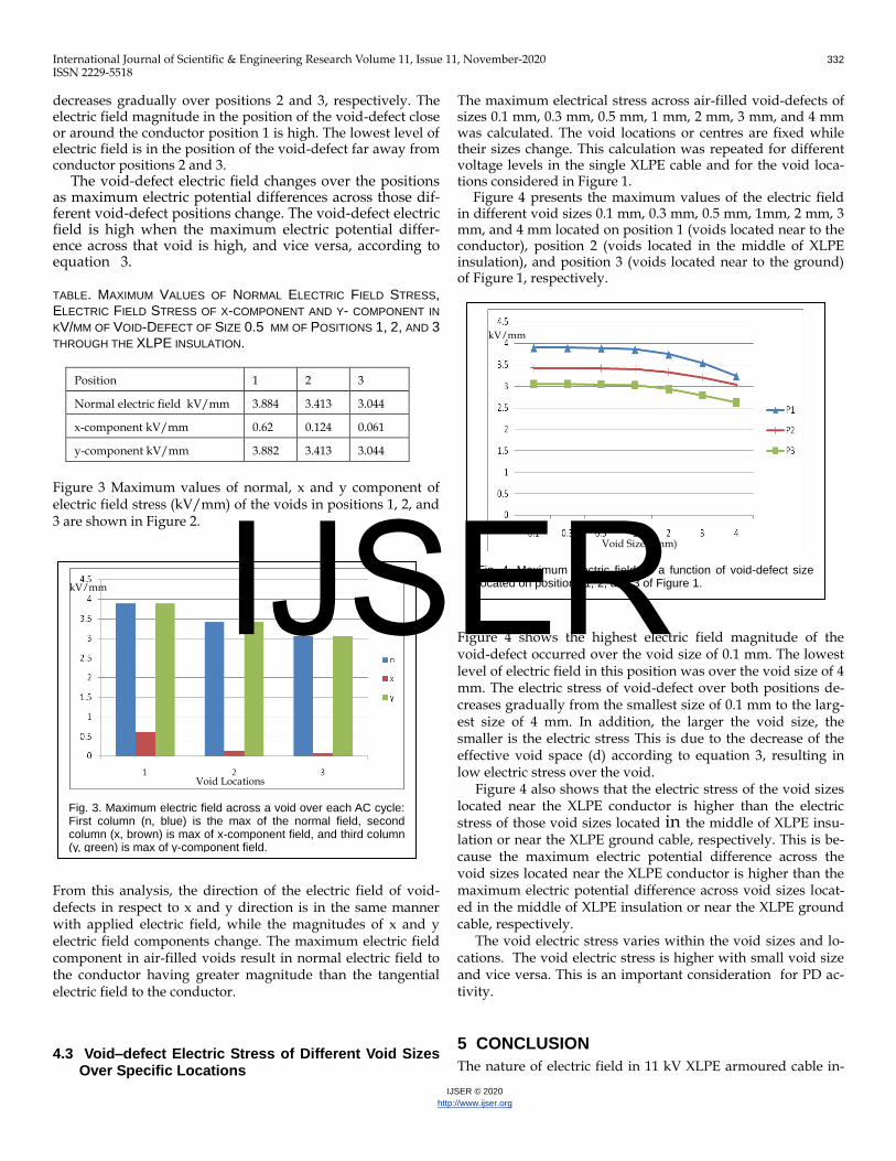
The void-defect electric field changes over the positions as maximum electric potential differences across those dif-ferent void-defect positions change. The void-defect electric field is high when the maximum electric potential differ-ence across that void is high, and vice versa, according to equation 3. TABLE. MAXIMUM VALUES OF NORMAL ELECTRIC FIELD STRESS, ELECTRIC FIELD STRESS OF X-COMPONENT AND Y- COMPONENT IN
KV/MM OF VOID-DEFECT OF SIZE 0.5 MM OF POSITIONS 1, 2, AND 3
THROUGH THE XLPE INSULATION.
Position 1 2 3
Normal electric field kV/mm 3.884 3.413 3.044
x-component kV/mm 0.62 0.124 0.061
y-component kV/mm 3.882 3.413 3.044
Figure 3 Maximum values of normal, x and y component of electric field stress (kV/mm) of the voids in positions 1, 2, and 3 are shown in Figure 2.
From this analysis, the direction of the electric field of void-defects in respect to x and y direction is in the same manner with applied electric field, while the magnitudes of x and y electric field components change. The maximum electric field component in air-filled voids result in normal electric field to the conductor having greater magnitude than the tangential electric field to the conductor.
4.3 Void–defect Electric Stress of Different Void Sizes Over Specific Locations
The maximum electrical stress across air-filled void-defects of sizes 0.1 mm, 0.3 mm, 0.5 mm, 1 mm, 2 mm, 3 mm, and 4 mm was calculated. The void locations or centres are fixed while their sizes change. This calculation was repeated for different voltage levels in the single XLPE cable and for the void loca-tions considered in Figure 1.
Figure 4 presents the maximum values of the electric field in different void sizes 0.1 mm, 0.3 mm, 0.5 mm, 1mm, 2 mm, 3 mm, and 4 mm located on position 1 (voids located near to the conductor), position 2 (voids located in the middle of XLPE insulation), and position 3 (voids located near to the ground) of Figure 1, respectively.
Figure 4 shows the highest electric field magnitude of the void-defect occurred over the void size of 0.1 mm. The lowest level of electric field in this position was over the void size of 4 mm. The electric stress of void-defect over both positions de-creases gradually from the smallest size of 0.1 mm to the larg-est size of 4 mm. In addition, the larger the void size, the smaller is the electric stress This is due to the decrease of the effective void space (d) according to equation 3, resulting in low electric stress over the void.
Figure 4 also shows that the electric stress of the void sizes located near the XLPE conductor is higher than the electric stress of those void sizes located in the middle of XLPE insu-lation or near the XLPE ground cable, respectively. This is be-cause the maximum electric potential difference across the void sizes located near the XLPE conductor is higher than the maximum electric potential difference across void sizes locat-ed in the middle of XLPE insulation or near the XLPE ground cable, respectively.
The void electric stress varies within the void sizes and lo-cations. The void electric stress is higher with small void size and vice versa. This is an important consideration for PD ac-tivity.
5 CONCLUSION
The nature of electric field in 11 kV XLPE armoured cable in-
Fig. 3. Maximum electric field across a void over each AC cycle: First column (n, blue) is the max of the normal field, second column (x, brown) is max of x-component field, and third column (y, green) is max of y-component field.
.
Fig. 4. Maximum electric field as a function of void-defect size located on positions 1, 2, and 3 of Figure 1.
Void Sizes (mm)
kV/mm
Void Locations
kV/mm IJSER

International Journal of Scientific & Engineering Research Volume 11, Issue 11, November-2020 333
ISSN 2229-5518
IJSER © 2020
http://www.ijser.org
sulation using finite element method software were devel-oped. Electrostatic consequences of voids in XLPE cable insu-lation material were investigated. The effect of the electric stress of different void-defect locations and sizes in MV XLPE insulted cable were presented. The void-defect electric stresses vary within their locations, sizes and direction of the applied field. The void-defect electric stress at high electric field back-ground is high and vice versa. The void-defect stress is high within small void-defect size and vice versa. The maximum electric field component in voids result in normal electric field to the conductor having greater magnitude than the tangential electric field to the conductor.
REFERENCES
[1] J. Veen, “On-line signal analysis of partial discharges in medium
voltage power cables,” Ph.D. dissertation, Dept. Elect. Eng., Tech-
nische Universiteit Eindhoven, Eindhoven, Netherlands, 2005.
[2] M. Kannan and P. Sreejaya, “Partial Discharge Detection in Solid
Dielectrics,”International Journal of Scientific and Engineering Research,
vol. 4, no. 8, August 2013.
[3] T. Seghir, D. Mahi, T. Lebey, and D. Malek, “Analysis of the electric
field and the potential distribution in cavities inside solid insulating
electrical materials,” Proceedings of the COMSOL Users Conference.
Pais, November. 2006.
[4] R. H. Bhuiyan, R. A. Dougal, and M. Ali, “Proximity coupled inter-
digitated sensors to detect insulation damage in power system ca-
bles,” IEEE sensors journal, vo l.7 no. 12 pp. 1589–1596, October. 2007.
[5] D. D. Chang, T. S. Sudarshan, and J. E. Thompson, “Analysis of
electric stress distribution in cavities embedded within dielectric
structures,” IEEE transaction on electrical insulation, Tema, May. 1986.
[6] D. Adhikari, D. M. Hepburn, and B. G. Stewart , “Analysis of deteri-
oration of PET insulation with multiple voids due to electrical stress-
ing,” IEEE Electrical Insulation Conference (EIC), Annapolis, 5-8 June.
2011.
[7] H. A. Illias, Q. L. Ng, A. H. A. Bakar, H. Mokhlis, and A. M. Ariffin, “
Electric field distribution in 132 kV XLPE cable termination model
from finite element method,” International Conference on Condition
Monitoring and Diagnosis (CMD), Bali , September. 2012.
[8] M. Alsharif , P. A. Wallace, D. M. Hepburn, and C Zhou, “FEM Mod-
elling of Electric Field and Potential Distributions of MV XLPE Ca-
bles Containing Void Defect,” Proceedings of the COMSOL Users Con-
ference. MILAN, pp 1-4, October. 2012 .
[9] T. William, Electrical Power Cable Engineering. 3rd ed. CRC Press,
pp.165-166, 2011.
IJSER