study of indium tin oxide (ito) for novel … of indium tin oxide (ito) for novel optoelectronic...
TRANSCRIPT
Study of Indium Tin Oxide (ITO) for
Novel Optoelectronic Devices
by
Shabbir A. Bashar B.Eng.
Submitted in accordance with the requirement for the Degree of Doctor of Philosophy
KING’S COLLEGE LONDON
University of London
Department of Electronic Engineering
1998

2
“¢hp¢jmÔ¡qÚ Bl-l¡qj¡e Bl-l¡¢qj”
To,
My parents
and
in loving memory of my grandparents
“k¡l¡ ü¢eiÑla¡l fb −M¡y−S, −M¡c¡ a¡−cl−L p¡q¡kÉ L−le”

3
Acknowledgments I would like to gratefully acknowledge the enthusiastic supervision of Dr. Ali Rezazadeh during this work. I thank Prof. Garth Swanson for the technical discussions on the spectral response model and Dr. S. E. Kanellopoulos for the help with optical measurements and relevant discussions. Postgraduates of the Physical Electronics Research Group are thanked for numerous stimulating discussions, help with experimental setup and general advice; in particular I would like to acknowledge the help of Dr. Jim Luck for his support. Sean Wootton, Kevin Smith and Nick Nicola are thanked for their assistance with all types of technical problems - at all times. I am grateful to all my friends from International Hall, University of London, for being the surrogate family during the many years I stayed there and for their continued moral support there after. From the staff, Donald Mann and Margaret Wilson are especially thanked for their care and attention. Finally, I am forever indebted to my parents and Anita for their understanding, endless patience and encouragement when it was most required. I am also grateful to Naela and Tanvir for their support. © 1998: Shabbir A. Bashar (in accordance with paragraph 8.2d, University of London Regulations for the Degrees of M.Phil. and Ph.D., October 1997) The Copyright of this thesis rests with Shabbir A Bashar, the author, and no quotation from it or information derived from it may be published without the prior written consent of the said author.

4
Abstract
Indium Tin Oxide (ITO) films were deposited on a number of semi-conductor materials using reactive r.f. sputtering technique to form both rectifying Schottky and ohmic contacts. These contacts were applied in the fabrication of a number of novel optoelectronic devices: Schottky photo-diodes, transparent gate High Electron Mobility Transistors (HEMTs), heterojunction bipolar transistors (HBTs) being used as heterojunction phototransistors (HPTs), light emitting diodes (LEDs) and vertical cavity surface emitting lasers (VCSELs). A number of these novel devices were studied in comparatively greater detail; these were the Schottky diode and the HPT. Deposition conditions necessary to produce ITO films with high conductivity and optical transparency over a wide spectral range were studied and optimised. Separate post deposition techniques were developed to produce near ideal rectifying contacts and ohmic contacts with low contact resistance respectively. A thin film of indium (In) was also used to optimise ITO ohmic contacts to n+ - GaAs substrates. Near ideal Schottky diodes were realised on n-GaAs substrates using aluminium (Al) and gold (Au) metal contacts. A simulation model was then developed and implemented to study the behaviour of current transport mechanisms over a wide temperature range. Photodiodes with ITO as the Schottky metal contact were fabricated and a study comprising of both their electrical and optical behaviour was undertaken. Relatively large geometry HBTs and HPTs were fabricated using AlGaAs/GaAs, InGaP/GaAs and InP/InGaAs systems respectively; the latter devices were first reported as a result of this study. A comparative study between devices fabricated from these systems were then made. This was followed by an appraisal of the electrical properties of each of their optical counterparts which had ITO emitter contacts. The specific photo responsivity and the spectral responses of these HPTs were analysed. In light of HPTs with transparent ITO emitter ohmic contacts, a brief examination of the merits of vertical versus lateral illumination was also made in this work. Finally a spectral response model was developed to understand and help design optoelectronic detectors comprising of single layer devices (n-GaAs Schottky photo diodes) or multiple semiconductor materials (HPTs using AlGaAs/GaAs or InP/InGaAs systems) to help predict responsivities at a given incident wavelength. As well as material properties of the constituent semiconductors, this model takes into account the specific lateral and vertical geometrical dimensions of the device.

List of Abbreviations, Constants and Symbols
5
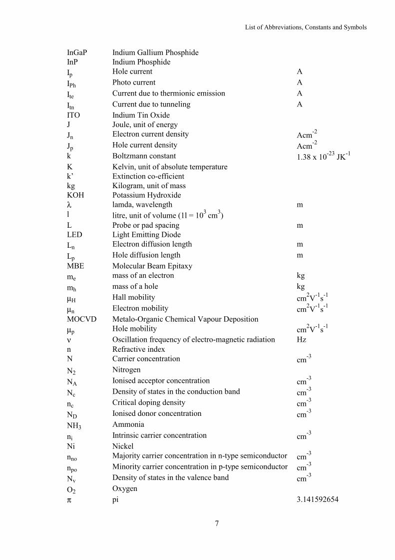
List of Abbreviations, Constants and Symbols
Symbol Meaning Units/Notes A Area m2 α Absorption co-efficient cm-2 Å Angstrom, unit of length (1Å = 10-10 m) A* Richardson constant Am-2K-2 A** Modified Richardson constant Am-2K-2 Al Aluminium Ar Argon As Arsenic Au Gold AuGe Gold-germanium eutectic alloy B Bandwidth β DC Current Gain of bipolar transistors BER Bit Error Rate BJT Bipolar Junction Transistor C Capacitance Farad, F c velocity of light in vacuum 3x10⁸ ms-1 χB Electron affinity of base V χE Electron affinity of emitter V Cf Correction factor CH4 Methane CO2 Carbon dioxide χs Electron affinity of a semiconductor eV CTO Cadmium Tin Oxide d Film thickness (or MESA height in TLM analysis) m D Diameter m δ Thickness of oxide layer m ∆Ec Conduction band offset at a heterojunction in eV eV ∆Eg Bandgap difference at a heterojunction in eV eV ∆Ev Valence band offset at a heterojunction in eV eV ∆φ Image-force induced reduction to barrier height eV Dn Electron diffusion constant cm2s-1 Dp Hole diffusion constant cm2s-1 Ds Density of surface states cm-2 ∆VCE0 Offset voltage V DVM Digital Volt Meter Ebr Breakdown electric field Vm-1 Ec Energy at the bottom of the conduction band in eV eV EDFA Erbium Doped Fiber Amplifier Ef Fermi level energy in eV eV

List of Abbreviations, Constants and Symbols
6
Eg Semiconductor bandgap in eV eV εo Permittivity of free space 8.8542 x 10⁻¹⁴ Fcm-1 Eo Tunneling constant Eoo Tunneling parameter εr Relative permittivity eV Electron volts, (1eV = 1.602x10⁻¹⁹ J) Ev Energy at the top of the valence band eV Φ Photon flux Φabs Photon flux absorbed in the semiconductor φb Barrier height V φbo Unbiased barrier height V FET Field Effect Transistor φm Work function of a metal V φn Barrier height to electrons in the emitter-base junction V φp Barrier height to holes in the base-emitter junction V Φref Reflected photon flux φs Work function of a semiconductor V G Optical gain Ga Gallium GaAs Gallium Arsenide Ge Germanium gm Transconductance of FETs h Planck constant 6.6262 x 10⁻³⁴ Js η Quantum efficiency H2 Hydrogen H2O Water H2O2 Hydrogen Peroxide H2SO4 Sulphuric acid H3PO4 Phosphoric acid HBT Heterojunction Bipolar Transistor HCl Hydrochloric acid HEMT High Electron Mobility Transistor HF Hydrofluoric acid hν Photon energy J HPT Heterojunction Photo Transistor I Current Amps, A Ib Base current (of a bipolar transistor) A Ic Collector current (of a bipolar transistor) A Ie Emitter current (of a bipolar transistor) A Igr Current due to generation-recombination A Ilk Leakage current A In Indium In Electron current A InGaAs Indium Gallium Arsenide
List of Abbreviations, Constants and Symbols
7
InGaP Indium Gallium Phosphide InP Indium Phosphide Ip Hole current A IPh Photo current A Ite Current due to thermionic emission A Itn Current due to tunneling A ITO Indium Tin Oxide J Joule, unit of energy Jn Electron current density Acm-2 Jp Hole current density Acm-2 k Boltzmann constant 1.38 x 10⁻²³ JK-1 K Kelvin, unit of absolute temperature k’ Extinction co-efficient kg Kilogram, unit of mass KOH Potassium Hydroxide λ lamda, wavelength m l litre, unit of volume (1l = 103 cm3) L Probe or pad spacing m LED Light Emitting Diode Ln Electron diffusion length m Lp Hole diffusion length m MBE Molecular Beam Epitaxy me mass of an electron kg mh mass of a hole kg µH Hall mobility cm2V-1s-1 µn Electron mobility cm2V-1s-1 MOCVD Metalo-Organic Chemical Vapour Deposition µp Hole mobility cm2V-1s-1 ν Oscillation frequency of electro-magnetic radiation Hz n Refractive index N Carrier concentration cm-3 N2 Nitrogen NA Ionised acceptor concentration cm-3 Nc Density of states in the conduction band cm-3 nc Critical doping density cm-3 ND Ionised donor concentration cm-3 NH3 Ammonia ni Intrinsic carrier concentration cm-3 Ni Nickel nno Majority carrier concentration in n-type semiconductor cm-3 npo Minority carrier concentration in p-type semiconductor cm-3 Nv Density of states in the valence band cm-3 O2 Oxygen π pi 3.141592654
List of Abbreviations, Constants and Symbols
8
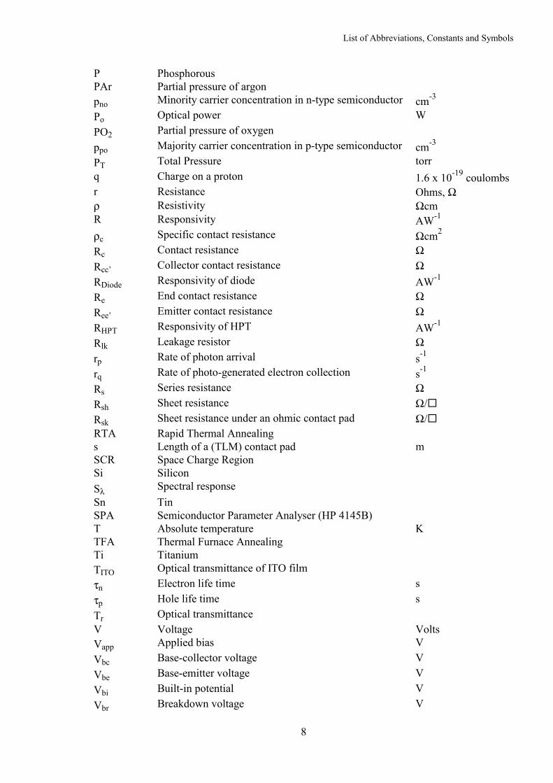
P Phosphorous PAr Partial pressure of argon pno Minority carrier concentration in n-type semiconductor cm-3 Po Optical power W PO2 Partial pressure of oxygen ppo Majority carrier concentration in p-type semiconductor cm-3 PT Total Pressure torr q Charge on a proton 1.6 x 10⁻¹⁹ coulombs r Resistance Ohms, Ω ρ Resistivity Ωcm R Responsivity AW-1 ρc Specific contact resistance Ωcm2 Rc Contact resistance Ω Rcc’ Collector contact resistance Ω RDiode Responsivity of diode AW-1 Re End contact resistance Ω Ree’ Emitter contact resistance Ω RHPT Responsivity of HPT AW-1 Rlk Leakage resistor Ω rp Rate of photon arrival s-1 rq Rate of photo-generated electron collection s-1 Rs Series resistance Ω Rsh Sheet resistance Ω/ Rsk Sheet resistance under an ohmic contact pad Ω/ RTA Rapid Thermal Annealing s Length of a (TLM) contact pad m SCR Space Charge Region Si Silicon Sλ Spectral response Sn Tin SPA Semiconductor Parameter Analyser (HP 4145B) T Absolute temperature K TFA Thermal Furnace Annealing Ti Titanium TITO Optical transmittance of ITO film τn Electron life time s τp Hole life time s Tr Optical transmittance V Voltage Volts Vapp Applied bias V Vbc Base-collector voltage V Vbe Base-emitter voltage V Vbi Built-in potential V Vbr Breakdown voltage V
List of Abbreviations, Constants and Symbols
9
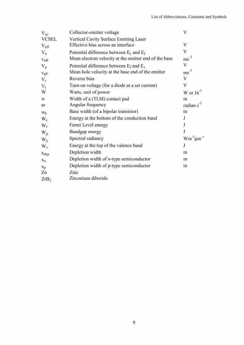
Vce Collector-emitter voltage V VCSEL Vertical Cavity Surface Emitting Laser Veff Effective bias across an interface V Vn Potential difference between Ec and Ef V vnB Mean electron velocity at the emitter end of the base ms-1 Vp Potential difference between Ef and Ev V vpE Mean hole velocity at the base end of the emitter ms-1 Vr Reverse bias V Vt Turn-on voltage (for a diode at a set current) V W Watts, unit of power W or Js-1 w Width of a (TLM) contact pad m ω Angular frequency radian s-1 wb Base width (of a bipolar transistor) m Wc Energy at the bottom of the conduction band J Wf Fermi Level energy J Wg Bandgap energy J Wλ Spectral radiancy Wm-2µm-1 Wv Energy at the top of the valence band J xdep Depletion width m xn Depletion width of n-type semiconductor m xp Depletion width of p-type semiconductor m Zn Zinc ZrB2 Zirconium diboride

Contents
10
Contents
Page no.
1. Introduction
1.1. Genesis 18
1.2. Aims and Objectives 19
1.3. Summary and Layout of Thesis 21
2. Background Theory and Literature Review
2.1. Indium Tin Oxide (ITO)
2.1.1. Introduction and Uses of ITO 22
2.1.2. Physical Structure and Properties of ITO 23
2.1.3. ITO Deposition Techniques 2.1.3.1. Sputtering 25 2.1.3.2. Thermal Evaporation 26 2.1.3.3. Spray Pyrolysis Technique 27 2.1.3.4. Screen Printing Technique 27
2.2. Schottky Contacts
2.2.1. Theory of Rectifying Metal Semiconductor Contacts 28
2.2.2. Current Transport Mechanisms in the Schottky Diode 30 2.2.2.1. Other Current Transport Mechanisms 31
2.2.2.2. φbo Barrier Lowering due to Image Force Effects 31 2.2.2.3. Generation-Recombination Effects 31 2.2.2.4. Current due to Quantum Mechanical Tunneling 32 2.2.2.5. Leakage Current 33

Contents
11
2.3. Ohmic Contacts
2.3.1. Theory of Ohmic Contacts 34
2.3.2. Practical Ohmic Contacts 35
2.4. Heterojunction Bipolar Transistors
2.4.1. Heterostructure Concepts 36
2.4.2. Current Transport in HBTs 39
2.4.3. Fundamental Advantages of HBTs 43
2.4.4. Abrupt Emitter-Base HBT 43
2.4.5. Common III-V HBT Material Systems 44
2.5. Optoelectronic Devices
2.5.1. The Case for Fiber-Optic Telecommunication 45 2.5.1.1. Submarine Optical Fiber Systems 47
2.5.2. Optical Detection Principles 48 2.5.2.1. The Key Parameters Relating a Photodetector to an Optical System 51
2.5.3. p-n, p-i-n and Avalanche Photodiodes (APDs) 52
2.5.4. ITO/n-GaAs Schottky Photodiodes 53
2.5.5. Transparent-Gate High Electron Mobility Transistors (TG-HEMTs) 54
2.5.6. Heterojunction Photo Transistors (HPTs) 55
2.5.7. Light Emitting Diodes (LED) and Vertical Cavity Surface Emitting Lasers (VCSEL) 56
2.5.8. Principal Receiver Configurations 57
2.5.9. A Brief Comparison between Various Types of Detectors 58
Contents
12
3. Device Fabrication and Processing
3.1. The Semiconductor Wafer
3.1.1. Compound Semiconductor Materials 60
3.1.2. Epitaxy 61 3.1.2.1. Epitaxial Lattice Matching 62
3.1.3. Growth Techniques: LPE, MOCVD, MBE 3.1.3.1. Liquid Phase Epitaxy - LPE 63 3.1.3.2. Metal Organic Chemical Vapour Deposition - MOCVD 64 3.1.3.3. Molecular Beam Epitaxy - MBE 66
3.2. ITO Deposition by Reactive r.f. Sputtering
3.2.1. Principles 68
3.2.2. The Nordiko 1500 r.f. Sputtering System 68
3.2.3. Controllability and Calibrations 69
3.2.4. Sample Preparation Prior to ITO Deposition 73
3.3. Photolithography 74
3.4. Metalisation by Resistive Thermal Evaporation 74
3.5. Wet Chemical Etching 76
3.6. Reactive Ion Etching 78
3.7. Thickness Monitoring and Calibration
3.7.1. Talystepping 79
3.7.2. Electrical Method 80
3.8. Annealing Methods
3.8.1. Thermal Furnace Annealing (TFA) 82
3.8.2. Rapid Thermal Annealing (RTA) 82
3.8.3. Annealing ITO Ohmic Contacts 83

Contents
13
3.9. Wafer Thinning Technique 84
3.10. Scribing, Packaging and Bonding 85
3.11. Processing Steps - the HBT Example 85
4. Measurement and Analysis Techniques
4.1. Transmission Line Model - TLM
4.1.1. Theory 89
4.1.2. Experimental Set-up 92
4.2. Current-Voltage Measurements (I-V)
4.2.1. Schottky Diode Parameter Extractions 93
4.2.1.1. Barrier Height, φbo 94 4.2.1.2. Ideality Factor, n 95
4.2.1.3. Series Resistance, Rs 95
4.2.2. Bipolar Transistor/HBT Parameter Extraction 95 4.2.2.1. Output Characteristics 95 4.2.2.2. Gummel Plot 96 4.2.2.3. D.C. Current Gain, β 96
4.2.2.4. Emitter and Collector Series Resistance, Ree’ and Rcc’ 96
4.2.3. FET/HEMT Parameter Extraction 4.2.3.1. Transfer Characteristics 97
4.2.3.2. Transconductance, gm 97
4.2.4. Experimental Set-up 98
4.3. Capacitance-Voltage Measurements (C-V)
4.3.1. Theory 99
4.3.2. Experimental Set-up 101
4.3.3. Limitations 102
Contents
14
4.4. Cryogenic Measurements 102
4.4.1. Experimental Set-up 103
4.5. Optical Measurements
4.5.1. ITO Film Characterisation 106
4.5.2. Device Quantum Efficiency and Absolute Responsivity 106
4.6. Spectral Response
4.6.1. Experimental Set-up 109
4.6.2. Deconvoluting Optical Non-linearities 110
5. Indium Tin Oxide (ITO): Experiment and Results
5.1. ITO Deposition - Results and Discussions
5.1.1. Accuracy of Measuring the Electrical Properties of ITO Films 112
5.1.2. Optical Properties of the Deposited ITO Films 116
5.1.3. Effect of Total Pressure 118
5.1.4. Effect of Oxygen Partial Pressure, PO2 119
5.1.5. Effect of r.f. Power 121
5.1.6. Effect of Induced Voltage 122
5.1.7. Effect of Deposition Rate 123
5.1.8. Effect of Target Pre-conditioning 124
5.1.9. Effect of Film Thickness 124
5.1.10. Effect of Target to Substrate Distance 125
5.1.11. Effect of Substrate Temperature During Deposition 126
5.2. Patterning ITO
5.2.1. ITO Patterning by Lift-off Lithography 126
5.2.2. Wet Chemical Etching 127
5.2.3. Effect of Adding Zn Dust to HCl Solution 129

Contents
15
5.2.4. Selective RIE of ITO in Argon Plasma 129
5.3. Post Deposition Treatments
5.3.1. Effects of Heat Treatment on the Electrical Properties of ITO 134 5.3.1.1. Schottky Annealing Scheme 134 5.3.1.2. Ohmic Annealing Scheme 137
5.3.2. Effects of Heat Treatment on the Optical Properties of ITO 137
5.3.3. Conclusion 138
5.4. Ohmic Contacts to ITO 139
5.4.1. Metalisation Schemes Used 140
5.4.2. Results and Conclusion 141
6. Application of Transparent ITO Contacts
6.1. Devices Based on the Schottky Contact
6.1.1. Results on Metal/n-GaAs Schottky Diodes 142 6.1.1.1. Diode Fabrication 142 6.1.1.2. I-V Results 144 6.1.1.3. Analysis and Modeling 147 6.1.1.4. Al/n-GaAs Schottky Diodes 154 6.1.1.5. Conclusion 155
6.1.2. Fabrication and Process Optimization for ITO/n-GaAs Schottky Diodes 155 6.1.2.1. The Effect of Mesa Etch and Post Deposition Annealing 156 6.1.2.2. Effect of r.f. Power and ITO Film Thickness 158 6.1.2.3. Diodes Fabricated at 150W r.f. Power Followed by Gradual
Annealing 160 6.1.2.3.1. ITO/In/n-GaAs Schottky Photodiodes - Sample A 162 6.1.2.3.2. ITO/n-GaAs Schottky Photodiodes - Sample B 171

Contents
16
6.1.2.4. Discussions and Conclusion 175
6.1.3. Richardson Constant for the ITO/n-GaAs Contact 178 6.1.3.1. Results and Discussion 178
6.1.4. Realisation of Transparent Gate HEMT using ITO 181 6.1.4.1. Fabrication 181 6.1.4.2. Results and Discussion 182
6.2. Devices Based on ITO Ohmic Contacts
6.2.1. ITO Ohmic Contacts to n+ and p+ Epitaxial Layers 183 6.2.1.1. Contacts to Highly Doped GaAs Epitaxial Layers 184
6.2.1.1.1. Fabrication and Post Deposition Annealing 184 6.2.1.1.2. Results and Comparison with Conventional Contacts 190
6.2.1.2. Contacts to Highly Doped InGaAs Epitaxial Layers 194 6.2.1.2.1. Fabrication and Post Deposition Annealing 194 6.2.1.2.2. Results and Comparison with Conventional Contacts 194
6.2.1.3. Surface Morphology of ITO Ohmic Contacts 196
6.2.2. Realisation of ITO Contacts to HPT Emitters 197 6.2.2.1. Fabrication of Conventional HBTs and ITO Emitter Contact HPTs 198 6.2.2.2. Electrical Properties of HBTs with Opaque and Transparent Contacts 202
6.2.2.2.1. AlGaAs/GaAs Devices 202 6.2.2.2.2. InGaP/GaAs Devices 211 6.2.2.2.3. InP/InGaAs Devices 213 6.2.2.2.4. Sputter Damage in HPT Devices 216 6.2.2.2.5. Comparison Between AlGaAs/GaAs, InGaP/GaAs and InP/InGaAs
HBTs 216 6.2.2.3. Optical Properties of HBTs 219
6.2.2.3.1. Output Characteristics 221 6.2.2.3.2. Spectral Response and Absolute Responsivity 224 6.2.2.3.3. Top versus Edge Coupling and Design Considerations 228
6.3. Spectral Response of Photodetectors 230
6.3.1. Spectral Properties of Relevant Materials 230
6.3.2. Spectral Response Model for a Monolayer Detector 234
6.3.3. Spectral Response of an ITO/n-GaAs Schottky Diode 238
6.3.4. Spectral Response of a HPT with ITO Emitter Contact 239
Contents
17
7. Conclusions 241
7.1. ITO Deposition 241
7.2. ITO-based Microfabrication 242
7.3. Optically Transparent Schottky Diodes 243
7.4. Transparent Gate HEMTs 245
7.5. Optically Transparent ITO Ohmic Contacts 245
7.6. Optically Transparent HPTs 246
7.7. Spectral Response Model 250
8. Further Work 251
References 252
Appendix A: List of Publications 270
Appendix B: Processing Steps for Lift-off and Etch Lithography 272
Appendix C: SPA Settings for Device Parameter Extractions 274
Appendix D: Mathematical Derivations 277
Chapter 1: Introduction
18
1. Introduction
1.1 Genesis With the demonstrated advantages of an optical fiber telecommunication system over a conventional copper-wire based system, the efficient conversion of an electrical signal to an optical signal and vice versa, is now of utmost importance. Similarly, rapid progress in semiconductor materials growth technology and the emergence of novel techniques in device fabrication has led to a continual improvement in the performance of opto-electronic integrated circuits (OEICs). In addition, with similar maturity in new technologies such as monolithic microwave integrated circuits (MMICs), the commercial viability of direct integration between optical and microwave circuits is becoming more and more likely. One of the vital components of any high frequency optical system is a large bandwidth, low noise photo receiver which may be realised using monolithic integration of photo diodes with high speed transistors to act as preamplifiers. A wide range of materials and devices, including semi-transparent metal/semiconductor Schottky photo diodes and integrated p-i-n diodes with HBTs have been used for this purpose. The use of a Schottky diode is ideal for high speed applications where it has many advantages. One of these is the inherent absence of any slow component associated with minority carrier effects. Its usage enables the absorption layer thickness to be engineered to obtain the optimum compromise between external quantum efficiency and detector bandwidth. The latter of these arises from a combination of carrier transit time and RC effects. An inherent disadvantage, however, is the high series resistance and low optical coupling efficiencies obtained which are associated with the thin semi-transparent metal layer. A solution to this problem is to use a layer of Indium Tin Oxide (ITO), a practically transparent and highly conductive material, as the Schottky contact to fabricate both high speed and highly efficient photo diodes. Renewed interest in using photo transistors as detectors has been aroused world wide, particularly with the advent of Heterojunction Bipolar Transistors (HBTs). Studies using such HBTs with opaque emitter contacts show excellent suitability of these devices as photo detectors in terms of optical performance where signal to noise ratios in excess of 30dB have been obtained. The optical gain of any photo transistor depends on the coupling efficiency,

Chapter 1: Introduction
19
the collection efficiency and its internal gain; in the HPT structure, there lies an inherent trade-off between the speed and the collection efficiency. However, by using a transparent emitter contact, the coupling efficiency can be significantly improved thereby raising the overall gain-bandwidth of the device correspondingly. Similar arguments could be presented in support of using a transparent ITO contact to a number of other devices such as in transparent gate HEMTs, LEDs and VCSELs. Hitherto, ITO had been the subject of extensive study by material scientists and engineers for a wide range of other applications ranging from anti-reflection coatings to transparent contacts in solar cells. Its usage in the fabrication of microelectronic devices for optoelectronic applications is a relatively new field. Hence, this study essentially represents some of the novel work in this area.
1.2 Aims and Objectives One of the primary objectives of this work was the application of a transparent ITO contact to a number of optoelectronic devices. These required the development of both Schottky and ohmic contacts. In particular, n-GaAs Schottky photo diodes and the heterojunction photo transistors, both as optical detectors, were studied in detail. With this goal in mind, the ITO film deposition based on a r.f. reactive sputtering technique was first studied and then optimised. Extensive work involving the calibration of the sputtering machine was carried out to understand the particular effects of various deposition conditions on the ITO films. These films were then characterised to study their electrical conductivity and optical transmittance. A number of different post-deposition annealing techniques were also developed for specific application as either Schottky or ohmic contacts. The use of a thin indium metallic layer between the sputtered ITO and the underlying semiconductor was also studied for its influence on sputter damage, ohmic and Schottky contacts. Work was also carried out to ensure that adequate patterning techniques were developed to realise small geometry devices based on ITO contacts. Similarly, contacts to ITO with pad metals was also studied and assessed. Once it was established that satisfactory ITO films could be produced, the work was extended to the fabrication of the devices. These films were used to realise novel optoelectronic devices which were characterised and compared to their opaque counterparts.

Chapter 1: Introduction
20
Schottky diodes with near ideal electrical characteristics were realised on n-GaAs substrates using aluminium (Al) and gold (Au) metal contacts. A simulation model was then developed and implemented to study the behaviour of current transport mechanisms over a wide temperature range. Photo diodes with ITO as the Schottky contact were fabricated and a study comprising of both their electrical and optical behaviour was undertaken. This involved further optimisation work to ensure the sputter damage sustained during the ITO deposition could be first minimised and then the remainder removed to an acceptable level without compromising the rectifying behaviour of the junction, reducing the series resistance and dark currents for photo diode operation. All this had to be carried out while retaining the desired high transparency and high conductivity properties of the ITO film itself. The next stage of the study involved the use of heterojunction transistors as photo detectors. Large geometry HBTs and HPTs were fabricated using AlGaAs/GaAs, InGaP/GaAs and InP/InGaAs systems respectively with both conventional and transparent ITO emitter ohmic contacts. A comparative study between devices fabricated from these systems were then made. This was followed by an appraisal of the electrical properties of each of their optical counterparts which had ITO emitter contacts. The specific photo responsivity and the spectral responses of these HPTs were analysed. In light of HPTs with transparent ITO emitter ohmic contacts, a brief examination of the merits of vertical versus lateral illumination was also made in this work. A spectral response model was also developed to understand and help design optoelectronic detectors comprising of single layer devices (n-GaAs Schottky photo diodes) or multiple semiconductor materials (HPTs using AlGaAs/GaAs or InP/InGaAs systems) to help predict responsivities at a given incident wavelength. As well as material properties of the constituent semiconductors, this model takes into account the specific lateral and vertical geometric dimensions of the device. In collaboration with other researchers, two by-products of this study were the first VCSEL and TG-HEMT using ITO as the transparent ohmic and Schottky gate contacts respectively. Some preliminary work was also carried out to produce ITO contacts to visible LEDs which had an emission wavelength of approximately 630nm.

Chapter 1: Introduction
21
1.3 Summary and Layout of Thesis In this thesis the background theory and the relevant literature survey are presented in the second chapter. This is followed, in chapter three, by a description of all the processing steps involved in the fabrication of the devices, while chapter four consists the details of the measurement and analysis techniques. Chapter five contains the first set of experimental results of this research; these are the findings concerning the ITO films used in the devices. Finally, chapter six constitutes the second and the larger part of results, namely that of the Schottky diodes and their temperature dependent current transport model, the heterojunction photo transistors, and the spectral response model respectively. The conclusion of the work and a list of suggestions for further work are presented in chapters seven and eight. A list of publications resulting from this work is given in Appendix A. Appendix B contains the processing steps for liftoff and etch lithography steps. Appendix C has the Hewlett Packard HP4145B Semiconductor Parameter Analyser (SPA) settings for the device parameter extractions while some mathematical derivations are given in Appendix D.

References
252
References: 1. K. L. Chopra, S. Major and D. K. Pandya, “Transparent Conductors - A Status
Review”, Thin Solid Films, 102, 1983, pp. 1 - 46, 2. S. A. Bashar and A. A. Rezazadeh, “Optically Transparent ITO Emitter Contacts in the
Fabrication of InP/InGaAs HPTs”, IEEE Transactions on Microwave Theory and Techniques, MTT-43(9), 1995, pp. 2299-2303
3. J. C. C. Fan and J. B. Goodenough, “X-Ray Photoemission Spectroscopy Studies of Sn-
doped Indium Oxide Films”Journal of Applied Physics, 48(8), 1977, pp. 3524 - 3531 4. P. Nath and R. F. Bunshah, “Preparation of In2O3 and Tin-Doped In2O3 Films by a
Novel Activated Reactive Evaporation Technique”, Thin Solid Films, 69, 1980, pp. 63 - 68
5. J. C. C. Fan, F. J. Bachner and G. H. Foley, “Effect of Oxygen Partial Pressure During
Deposition on Properties of r.f. Sputtered Sn-Doped In2O3 Films”, Applied Physics Letters, 31(11), 1977, pp. 773 - 775
6. K. Sreenivas, T. Sundarsena Rao, A. Mansnigh and S. Chandra, “Preparation and
Characterization of r.f. Sputtered Indium Tin Oxide Films”, Journal of Applied Physics, 57(2), 1985, pp. 384 - 392
7. J. Szczyrbowski, A. Dietrich and H. Hoffmann, “Optical and Electrical Properties of r.f.
Sputtered Indium-Tin Oxide Films”, Phys Stat Sol (a), 78, 1983, pp. 243 - 252 8. M. Buchanan, J. B. Webb and D. F. Williams, “The Influence of Target Oxidation and
Growth Related Effects on the Electrical Properties of Reactively Sputtered Films of Tin-Doped Indium Oxide”, Thin Solid Films, 80, 1981, pp. 373 - 382
9. M. Higuchi, S. Uekusa, R. Nakano and K. Yokogawa, “Post-Deposition Annealing
Influence on Sputtered Indium Tin Oxide Film Characteristics”, Japanese Journal of Applied Physics, 33, 1994, pp. 302 - 306
10. N. Balasubramanian and A. Subrahmanyam, “Effect of Substrate Temperature on the
Electrical and Optical Properties of Reactively Evaporated Indium Tin Oxide Films”, Materials Science and Engineering, B1, 1988, pp. 279 - 281
11. J. Bregman, Y. Shapira and H. Aharoni, “Effects of Oxygen Partial Pressure During
Deposition on the Properties of Ion-Beam-Sputtered Indium-Tin Oxide Thin Films”, Journal of Applied Physics, 67(8), 1990, pp. 3750 - 3753
12. H. Haitjema and J. J. Ph. Elich, “Physical Properties of Pyrolitically Sprayed Tin-
Doped Indium Oxide Coatings”, Thin Solid Films, 205, 1991, pp. 93 - 100
References
253
13. N. Balasubramanian and A. Subrahmanyam, “Electrical and Optical Properties of Reactively Evaporated Indium Tin Oxide (ITO) Films - Dependence on Substrate Temperature and Tin Concentration”, Journal of Physics D: Applied Physics, 22, 1989, pp. 206 - 209
14. L. Gupta, A. Mansingh and P. K. Srivastava, “Band Gap Narrowing and the Band
Structure of Tin Doped Indium Oxide Films”, Thin Solid Films, 176, 1989, pp. 33 - 44 15. J. L. Yao, S. Hao and J. S. Wilkinson, “Indium Tin Oxide Films by Sequential
Evaporation”, Thin Solid Films, 189(2), 1990, pp. 227 - 233 16. J. Dutta and S. Ray, “Variations in Structural and Electrical Properties of Magnetron-
Sputtered Indium Tin Oxide Films with Deposition Parameters”, Thin Solid Films, 162(1-2), 1988, pp. 119 - 127
17. S. Ashok, P. P. Sharma and S. J. Fonash, “Spray-Deposited ITO-Silicon SIS
Heterojunction Solar Cells”, IEEE Transactions on Electron Devices, ED-27(4), 1980, pp. 725 - 730,
18. B. Bessais, N. Mliki and R. Bennaceur, “Technological, Structural and Morphological
Aspects of Screen-Printed ITO Used in ITO/Si Type Structure”, Semiconductor Science and Technology, 8, 1993, pp. 116 - 121
19. E. H. Rhoderick, “Metal-Semiconductor Contacts” IEE Proceedings-I Solid-State and
Electron Devices, 129(1), 1982, pp. 1 - 14 20. E. H. Rhoderick and R. H. Williams, “Metal-Semiconductor Contacts”, (Publishers:
Clarendon Press, Oxford), 2nd Edition, 1988 21. F. A. Padovani and R. Stratton, “Field and Thermionic-Field Emission in Schottky
Barriers”, Solid State Electronics, 9, 1966, pp 695 - 707 22. D. Donoval, M. Barus and M. Zdimal, “Analysis of I-V Measurements on PtSi-Si
Schottky Structures in a Wide Temperature Range”, Solid State Electronics, 34(12), 1991, pp 1365 - 1373
23. S. M. Sze, “Metal-Semiconductor Contacts”, in Physics of Semiconductor Devices,
(Publishers: J Wiley & Sons, Singapore), 2nd Edition 1981, pp 250 - 254 24. C. R. Crowell and V. L. Rideout, “Normalised Thermionic-Field (T-F) Emission in
Metal-Semiconductor (Schottky) Barriers”, Solid State Electronics, 12, 1969, pp 89 - 105
25. V. L. Rideout, “A Review of the Theory and Technology for Ohmic Contacts to Group
III-V Compound Semiconductors”, Solid State Electronics, 18, 1975, pp. 541 - 550 26. A. Piotrowska, A. Guivarc’h and G. Pelous, “Ohmic Contacts to III-V Compound
Semiconductors: A Review of Fabrication Techniques”, Solid State Electronics, 26(3), 1983, pp. 179 - 197

References
254
27. J. Gyulai, J. W. Mayer, V. Rodriguez, A. Y. C. Yu and H. J. Copen, “Alloying
Behaviour of Au and AuGe on GaAs”, Journal of Applied Physics, 42(9), 1971, pp. 3578 - 3585
28. F. Lønnum, J. S. Johannessen, “Effect of Au:Ge Thickness on Ohmic Contacts to
GaAs”, Electronics Letters, 22(12), 1986, pp. 632 - 633 29. F. Ren, A. B. Emerson, S. J. Pearton, T. R. Fullowan and J. M. Brown, “Improvement
of Ohmic Contacts on GaAs with In Situ Cleaning”, Applied Physics Letters, 58(10), 1991, pp. 1030 - 1032
30. C. L. Chen, L. J. Mahoney, M. C. Finn, R. C. Brooks, A. Chu and J. G. Mavroides,
“Low Resistance Pd/Ge/Au and Ge/Pd/Au Ohmic Contacts to n-type GaAs”, Applied Physics Letters, 48(8), 1986, pp. 535 - 537
31. J. T. Lai and J. Y. Lee, “Redistribution of Constituent Elements in Pd/Ge Contacts to n-
type GaAs Using Rapid Thermal Annealing”, Journal of Applied Physics, 76(3), 1994, pp. 1686 - 1690
32. T. Sanada and O. Wada, “Ohmic Contacts to p-GaAs with Au/Zn/Au Structure”,
Japanese Journal of Applied Physics, 49(8), 1980, pp. L491 - L494 33. A. Katz, C. R. Abernathy and S. J. Pearton, “Pt/Ti Ohmic Contacts to Ultrahigh Carbon
Doped p-GaAs Formed by Rapid Thermal Processing”, Applied Physics Letters, 56(11), 1990, pp. 1026 - 1030
34. W. L. Chen, J. C. Cowles, G. I. Haddad, G. O. Munns, K. W. Eisenbeiser and J. R.
East, “Ohmic Contact Study for Quantum Effect Transistors and Heterojunction Bipolar Transistors with InGaAs Contact Layers”, Journal of Vacuum Science and Technology, B10(6), 1992, pp. 2354 - 2360
35. A. Katz, A. El-Roy, A. Feingold, M. Geva, N. Moriya, S. J. Pearton, E. Lane, T. Keel
and C. R. Abernathy, “W(Zn) Selectively Deposited and Locally Diffused Ohmic Contacts to p-InGaAs/InP Formed by Rapid Thermal Low Pressure Metalorganic Chemical Vapor Deposition”, Applied Physics Letters, 62(21), 1993, pp. 2652 - 2654
36. W. Shockley, US Patent no. 2 569 347, 1951 37. H. Kromer, “Theory of a Wide-Gap Emitter for Transistors”, Proceedings of the IRE,
45, 1957, pp. 1535 - 1537 38. H. Kromer, “Heterostructure Bipolar Transistors and Integrated Circuits”, Proceedings
of the IEEE, 70(1), 1982, pp. 13-25 39. M. B. Das, “HBT Device Physics and Models” in HEMTs and HBTs: Devices,
Fabrication and Circuits, (Editors: F. Ali and A. Gupta; Publishers: Artech House Inc., USA), Chapter 4, 1991, pp. 191 - 251

References
255
40. J. Batey and S. L. Wright, “Energy Band Alignment in GaAs:(Al,Ga)As Heterostructures: The Dependence on Alloy Compositions”, Journal of Applied Physics, 59(1), 1986, pp. 200 - 209
41. T. Kobayashi, K. Taira, F. Nakamura and H. Kawai, “Band Lineup for a GaInP/GaAs
Heterojunction Measured by a High Gain N-p-n Heterojunction Bipolar Transistor Grown by Metalorganic Chemical Vapor Deposition”, Journal of Applied Physics, 65(12), 1989, pp. 4898 - 4902
42. D. Biswas, N. Debbar, P. Bhattacharya, “Conduction and Valence Band Offsets in
GaAs/Ga0.51In0.49P Single Quantum Wells Grown by Metal Chemical Vapor Deposition”, Applied Physics Letters, 56(9), 1990, pp. 833 - 835
43. M. A. Rao, E. J. Caine, H. Kroemer, S. I. Long and D. I. Babic, “Determination of
Valence and Conduction Band Discontinuities at the (Ga, In)P/GaAs Heterojunction by C-V Profiling”, Journal of Applied Physics, 61(2), 1987, pp. 643 - 649
44. D. V. Lang, M. B. Panish, F. Capasso, J. Allam, R. A. Hamm, A. M. Sergent and W. T.
Tsang, “Measurement of Heterojunction Band Offsets by Admittance Spectroscopy: InP/Ga0.47In0.53As”, Applied Physics Letters, 50(12), 1987, pp. 736 - 738
45. P. M. Asbeck, M. C. F. Chang, J. A. Higgins, N. H. Sheng, G. J. Sullivan, K. C. Wang
“GaAlAs/GaAs Heterojunction Bipolar Transistors: Issues and Prospects for Application”, IEEE Transactions on Electron Devices, ED-36(10), 1989, pp. 2032 - 2042
46. D. V. Morgan and A. A. Rezazadeh, “Current Transport Mechanism in N-p-n
GaAs/AlGaAs Heterojunction Bipolar Transistors”, GEC Journal of Research, 6(1), 1988, pp. 37 - 43
47. G. O. Ladd and D. L. Feucht, ‘Performance Potential of High Frequency Heterojunction
Transistors’, IEEE Transactions on Electron Devices, 17, 1970, pp. 413 - 420 48. W. A. Hughes, A. A. Rezazadeh and C. E. Wood, “The Heterojunction Bipolar
Transistor (HBT)” in GaAs Integrated Circuits, (Editor: J. Mun; Publishers: Blackwell Scientific Publications Ltd, UK), Chapter 7, 1988, pp. 403 - 429
49. R. A. Hamm, M. B. Panish, R. N. Nottenburg, Y. K. Chen and D. A. Humphrey,
“Ultrahigh Be Doping of Ga0.47In0.53As/InP by Low-Temperature Molecular Beam Epitaxy”, Applied Physics Letters, 54(25), 1989, pp. 2586 - 2588
50. Y. K. Chen, R. N. Nottenburg, M. B. Panish, R. A. Hamm and D. A. Humprey, “Sub-
picosecond InP/InGaAs Heterojunction Transistors”, IEEE Electron Device Letters, 10(6), 1989, pp. 267 - 269
51. S. R. Forrest, “Monolothic Optoelectronic Integration: A New Component Technology for Lightwave Communications”, IEEE Transactions on Electron Devices, 32(12), 1985, pp. 2640 - 2655
References
256
52. D. Reudink, ‘Advanced Concepts and Technologies for Communications Satellites’ in Advanced Digital Communications, (Editor: K. Feher; Publishers: Prentice Hall, USA), Chapter 11, 1987.
53. T. Miya, Y. Terunuma, T. Hosaka and T. Miyashita, “Ultimate Low Loss Single-Mode
Fiber at 1.55 µm”, Electronic Letters, 15, 1979, pp. 106 - 108 54. S. E. Miller and I. P. Kaminow, ‘Optical Fiber Telecommunications II’, (Publishers:
Academic Press Inc., USA), 1988 55. P. Cochrane, D. J. T. Heatley, P. P. Smyth and I. D. Pearson, “Optical
Telecommunications - Future Prospects”, Electronics and Communication Engineering Journal, Aug. 1993, pp. 221 - 232
56. D. K. Paul, K. H. Greene and G. A. Keopf, “Undersea Fiber Optic Cable
Communication System of the Future: Operational, Reliability and System Considerations”, IEEE Journal of Lightwave Technology, LT-2(4), 1984, pp. 414 - 425
57. P. K. Runge and P. R. Trischitta, “The SL Undersea Lightwave System”, IEEE Journal
of Selected Areas in Communications, SAC-2(6), 1984, pp.784 - 793 58. K. Amano, “Optical Fiber Submarine Cable Systems”, IEEE Journal of Lightwave
Technology, 8(4), 1990, pp. 595 - 609 59. P. K. Runge, “Undersea Lightwave Systems”, AT&T Technical Journal, 71(1), 1992,
pp. 5 - 13 60. Blanc et al, “Optical Fiber Submarine Transmission Systems”, in Commutations and
Transmission, (Publishers: SOTELEC, France), 1989, pp.75 - 94 61. J. M. Senior, “Optical Fiber Communications”, (Published by: Prentice Hall Inc., New
Jersey, USA), 2nd Edition, 1992 62. M. Brain and T. Lee, “Optical Receivers for Lightwave Communication Systems”,
IEEE Transactions on Electron Devices, ED-32(12), 1985, pp. 2673 - 2692 63. T. Lee, C. A. Burrus and A. G. Dentai, “InGaAs/InP p-i-n Photodiodes for Lightwave
Communications at the 0.95 - 1.65 µm Wavelength”, IEEE Journal of Quantum Electronics, QE-17(2), 1981, pp. 232 - 238
64. T. P. Pearsall, M. Piskorski, A. Brochet and J. Chevrier, “A Ga0.47In0.53As/InP
Heterophotodiode with Reduced Dark Current”, IEEE Journal of Quantum Electronics, QE-17(2), 1981, pp. 255 - 259
65. J. E. Bowers and C. A. Burrus, “Ultrawide-Band Long-Wavelength p-i-n Photodetectors”, Journal of Lightwave Technology, LT-5(10), 1987, pp. 1339 - 1350
66. H. Ando, Y. Yamauchi, H. Nakagome, N. Susa and H. Kanbe, “InGaAs/InP Separated
Absorption and Multiplication Regions Avalanche Photodiode Using Liquid-and-

References
257
Vapor-Phase Epitaxies”, IEEE Journal of Quantum Electronics, QE-17(2), 1981, pp. 250 - 254
67. J. C. Campbell, A. G. Dentai, W. S. Holder and B. L. Kasper, “High Performance
Avalanche Photodiode with Separate Absorption ‘Grading’ and Multiplication Regions”, Electronics Letters, 19, 1983, pp. 818 - 820
68. F. Capasso, W. T. Tsang, A. L. Hutchinson and G. F. Williams, “Enhancement of
Electron Impact Ionization in a Superlattice: A New Avalanche Photodiode with a Large Ionization Rate Ratio”, Applied Physics Letters, 40(1), 1982, pp. 38 - 40
69. T. Kagawa, H. Asai and Y. Kawamura, “An InGaAs/InAlAs Superlattice Avalanche
Photodiode with a Gain Bandwidth Product of 90 GHz”, IEEE Photonics Technology Letters, 3(9), 1991, pp. 815 - 817
70. D. G. Parker and P. G. Say, “Indium Tin Oxide/GaAs Photodiodes for Millimetric-
Wave Applications”, Electronics Letters, 22(23), 1986, pp. 1266 - 1267 71. S. Y. Wang and D. M. Bloom, “100 GHz Bandwidth Planar GaAs Schottky
Photodiode”, Electronics Letters, 19, 1983, pp. 554 - 555 72. N. Emeis, H. Schumacher and H. Beneking, “High Speed GaInAs Schottky
Photodetector”, Electronics Letters, 21(5), 1985, pp. 180 - 181 73. D. G. Parker, P. G. Say and A. M. Hansom, “110 GHz High Efficiency Photodiodes
Fabricated from Indium Tin Oxide/GaAs”, Electronics Letters, 23, 1987, pp. 527 - 528 74. A. A. De Salles, M. A. Romero, “Al0.3Ga0.7As/GaAs MESFETs Under Optical
Illumination”, IEEE Transactions on Microwave Theory and Techniques, MTT-39(12), 1991, pp. 2010 - 2017
75. R. N. Simons, “Microwave Performance of an Optically Controlled AlGaAs/GaAs
High Electron Mobility Transistor and GaAs MESFET”, IEEE Transactions on Microwave Theory and Techniques, MTT-35(12), 1987, pp. 1444 - 1455
76. J. Seymour, “Field Effect Transistors and Charge Transfer Devices” in Electronic
Devices and Components, (Publishers: Longman Scientific and Technical, UK), Second Edition, Chapter 6, 1988, pp. 258 - 320
77. W. A. Hughes, A. A. Rezazadeh and E. C. Wood, “The High Electron Mobility
Transistor” in GaAs Integrated Circuits, (Editor: J. Mun; Publishers: Blackwell Scientific Publications Ltd, UK), Chapter 7, 1988, pp. 378 - 402
78. P. Chakrabarti, N. L. Shrestha, S. Srivastava and V. Khemka, “An Improved Model of Ion-Implanted GaAs OPFET”, IEEE Transactions on Electron Devices, ED-39(9), 1992, pp. 2050 - 2059
79. A. H. Khalid, S. A. Bashar and A. A. Rezazadeh,”Fabrication and Characterisation of a Transparent Gate HEMT Using Indium Tin Oxide” Proceedings of IEEE International
References
258
Workshop on High Performance Electron Devices for Microwave and Optoelectronic Applications - EDMO, London, UK, 14th November, 1994, pp. 99-104
80. K. Tabatabaie-Alavi and C. G. Fonstad (Jr), “Performance Comparison of
Heterojunction Phototransistors, p-i-n FET’s, and APD-FETs for Optical Fiber Communication Systems”, IEEE Journal of Quantum Electronics, QE-17(12), 1981, pp. 2259 - 2261
81. H. Wang, C. Bacot, C. Gerard, J. L. Lievin, C. Dubon-Chevallier, D. Ankri and A.
Scavennec, “GaAs/GaAlAs Heterojunction Bipolar Phototransistor for Monolithic Photoreceiver Operating at 140Mbit/s”, IEEE Transactions on Microwave Theory and Techniques, MTT-34(12), 1986, pp. 1344 - 1348
82. H. Beneking, P. Mischel and G. Schul “High-Gain Wide-Gap-Emitter Ga1-xAlxAs-
GaAs Phototransistor”, Electronics Letters, 12(16), 1976, pp. 395 - 396 83. Z. Urey, D. Wake, D. J. Newson and I. D. Henning, “Comparison of InGaAs
Transistors as Optoelectronic Mixers”, Electronic Letters, 29(20), 1993, pp. 1796 - 1797
84. T. Moriizumi and K. Takahashi, “Theoretical Analysis of Heterojunction
Phototransistors”, IEEE Transactions on Electron Devices, ED-19(2), 1972, pp. 152 - 159
85. R. A. Milano, P. D Dapkus and G. E. Stillman, “An Analysis of the Performance of
Heterojunction Phototransistors for Fiber Optic Communications”, IEEE Transactions on Electron Devices, ED-29(2), 1982, pp. 266 - 274
86. S. Sze, “LED and Semiconductor Lasers” in Physics of Semiconductor Devices,
(Publishers: John Wiley and Sons, NY), Second Edition, Chapter 12, 1981, pp. 681 - 742
87. Y. H. Aliyu, D. V. Morgan, H. Thomas and S. W. Bland, “Low Turn-on Voltage
AlGaInP LEDs Using Thermally Evaporated Transparent Conducting Indium Tin Oxide (ITO)”, Proceedings of IEEE International Workshop on High Performance Electron Devices for Microwave and Optoelectronic Applications - EDMO, London, UK, 14th November, 1995, pp. 82 - 87
88. M. A. Matin, A. F. Jezierski, S. A. Bashar, D. E. Lacklison, T. M. Benson, T. S. Cheng,
J. S. Roberts, T. E. Sale, J. W. Orton, C. T. Foxon and A. A. Rezazadeh, “Optically Transparent Indium Tin Oxide (ITO) Ohmic Contacts in the Fabrication of Vertical Cavity Surface Emitting Lasers”, Electronic Letters, 30(4), 1994, pp. 318 - 320 (and 532)
89. L. D. Tzeng and R. E. Frahm, “Wide Bandwidth Low Noise p-i-n/FET Receiver for High-Bit-Rate Optical Preamplifier Applications”, Electronics Letters, 24(18), 1988, pp. 1132 - 1133

References
259
90. S. Chandrasekhar, L. M. Lunardi, A. H. Gnauck, D. Ritter, R. A. Hamm, M. B. Panish and G. J. Qua, “A 10 Gbit/s OEIC Photoreceiver Using InP/InGaAs Heterojunction Bipolar Transistors”, Electronics Letters, 28(5), 1992, pp. 466 - 468
91. W. A. Hughes and D. G. Parker, “Operation of a High Frequency Photodiode-HEMT
Hybrid Photoreceiver at 10 GHz”, Electronics Letters, 22(10), 1986, pp. 509 - 510 92. J. L. Gimlett, “Low Noise p-i-n/FET Optical Receiver”, Electronics Letters, 23(6),
1987, pp. 281 - 283 93. M. A. R. Violas, D. J. T. Heatley, X. Y. Gu, D. A. Cleland and W. A. Stallard,
“Heterodyne Detection at 4 Gbit/s Using a Simple p-i-n/HEMT Receiver”, Electronics Letters, 27(1), 1991, pp. 59 - 61
94. D. Wake, R. H. Walling, I. D. Henning and D. G. Parker “Planar-Junction, Top-
Illuminated GaInAs/InP p-i-n photo diode with Bandwidth of 25 GHz”, Electronics Letters, 25(15), 1989, pp. 967 - 968
95. D. Wake, D. J. Newson, M. J. Harlow and I. D. Henning, “Optically Biased, Edge-
Coupled InP/InGaAs Heterojunction Phototransistors”, Electronics Letters, 29(25), 1993, pp. 2217 - 2218
96. W. Q. Li, M. Karakucuk, J. Kulman, J. R. East, G. I. Haddad and P. K. Bhattacharya,
“High Frequency GaAs/Al0.25Ga0.75As Heterojunction Bipolar Transistors with Transparent Indium Tin Oxide Emitter Contacts”, Electronics Letters, 29(25), 1993, pp. 2223 - 2225
97. D. W. Pashley, “The Basics of Epitaxy” in Growth and Characterisation of
Semiconductors, (Editors: R. A. Stradling and P. C. Klipstein; Publishers: Adam Hilger, New York), 1990, pp. 1 - 16
98. B. G. Streetman, “Crystal Properties and Growth of Semiconductors” in Solid State
Electronic Devices, (Publishers: Prentice-Hall, New Jersey, USA), 1980, pp. 1 - 27 99. J. O. Williams, “Metal Organic Chemical Vapour Deposition (MOCVD) for the
Preparation of Semicondutor Materials and Devices” in Growth and Characterisation of Semiconductors, (Editors: R. A. Stradling and P. C. Klipstein; Publishers: Adam Hilger, New York), 1990, pp. 17 - 33
100. M. Lundstrom, “III-V Heterojunction Bipolar Transistors”, in Heterojunction
Transistors and Small Size Effects in Devices, (Editor: M. Willander, Publishers: Studentlitteratur, Sweden), 1992, pp. 35 - 46
101. C. T. Foxon and B. A. Joyce, “Growth of Thin Films and Heterostructures of III-V
Compounds by Molecular Beam Epitaxy”, in Growth and Characterisation of Semiconductors, (Editors: R. A. Stradling and P. C. Klipstein; Publishers: Adam Hilger, New York), 1990, pp. 35 - 64

References
260
102. R. V. Stuart, “Vacuum Technology, Thin Films and Sputtering”, (Published by: Academic Press, London) Chapter 4, 1983, pp. 123 - 131
103. J. L. Vossen and J. J. Cuomo, “Glow Discharge Sputter Deposition” in Thin Film
Processes, (Editors: J. L. Vossen and Werner Kern, Publishers: Academic Press, New York), Part II-1, 1978, pp. 12 - 73
104. “Handbook On RF Sputtering with the NM 1500 Sputtering Module”, Nordiko Ltd.,
Brockhampton Lane, Havant, Hants. PO9 1JB, U.K. 105. Available from: “Ablestik Electronic Materials and Adhesive” subsidiary of “National
Starch and Chemical Co.”, 20021 Susana Road, Rancho Dominguez, CA 90221, USA 106. Source of ITO sputtering targets: “Testbourne Ltd.”, Unit 12, Hassocks Wood, Stroudly
Road, Basingstoke, Hampshire RG24 0NE, UK 107. R. C. Jaeger, “Lithography” in Introduction to Microelectronic Fabrication, Modular
Series on Solid State Devices, (Series Edited by: G. W. Neubeck, R. F. Pierret, Published by: Addison-Wesley Publishing Co. Inc., New York), Vol. 5, Chapter 2, 1988, pp. 13 - 28
108. K. L. Chopra and I. Kaur, “Thin Film Device Applications”, (Published by: Plenum
Press, New York) Chapter 1, 1983, pp. 14 - 18 109. R. V. Stuart, “Vacuum Technology, Thin Films and Sputtering”, (Published by:
Academic Press, London) Chapter 3, 1983, pp. 65 - 89 110. R. E. Williams, “Wet Etching” in Gallium Arsenide Processing Technology, (Published
by: Artech House, Massachussetts) Chapter 5, 1984, pp. 101 - 123 111. W. Kern and C. A. Deckert, “Etching Processes” in Thin Film Processes” (Edited by :
J. L. Vossen and W. Kern; Published by Academic Press, London) Part V, 1978, pp. 401 - 496
112. M. Konagai, K. Katsukawa and K. Takahashi, “(GaAl)As/GaAs Heterojunction
Phototransistors with High Current Gain”, Journal of Applied Physics, 48(10), 1977, pp. 4389 - 4394
113. C. M. Melliar-Smith and C. J. Mogab, “Plasma Assisted Etching Techniques for Pattern
Delineation” in Thin Film Processes, (Editors: J. L. Vossen and Werner Kern, Publishers: Academic Press, New York), Part V, 1978, pp. 497 - 556
114. Plasma Technology (UK) Ltd., Lawrence Rd., Wrington, Avon BS18 7QF, UK 115. “Talystep Operating Instructions”, Rank Taylor Hobson Ltd., P. O. Box 36, Newstar
Rd., Thurmaston Lane, Leicester LE4 7JQ, UK

References
261
116. J. Bitsakis, “Atomic Force Microscopy” in Non-Alloyed Ohmic Contacts to n-GaAs Grown by MBE, University of Manchester Institute of Science and Technology, M.Sc. Thesis 1996, Chapter 5, pp. 77 - 99
117. J. Seymour, “Reverse Breakdown Mechanisms” in Electronic Devices and
Components, (Published by: Longman Scientific and Technical, Essex, UK), Chapter 3, Second Edition, 1988, pp. 110 - 117
118. Available from Promatech Ltd., Unit E&F, The Old Brickyard, Aston Keynes,
Wiltshire SN6 6QX, UK 119. G. K. Reeves and H. B. Harrison, “Obtaining the Specific Contact Resistance from
Transmission Line Model Measurements”, IEEE Transactions on Electron Devices, EDL-3(5), 1982, pp. 111 - 113
120. H. B. Harrison, “Characterising Metal Semiconductor Ohmic Contacts”, Proceedings of
IREE, 41, 1980, pp. 95 - 100 121. F. Amin, “TLM Measurements using Auto-TLM System”, M.Phil. Transfer Report,
King’s College London, 1995, pp. 17 - 19 122. T. C. Lee, S. Fung, C. D. Beling and H. L. Au, “A Systematic Approach to the
Measurement of Ideality Factor, Series Resistance and Barrier Height for Schottky Diodes”, Journal of Applied Physics, 72(10), 1992, pp. 4739 - 4742
123. E. K. Evangelou, L. Papadimitriou, C. A. Dimitriades, G. E. Giakoumakis, “Extraction
of Schottky Diode (and p-n Junction) Parameters from I-V Characteristics”, Solid State Electronics, 36(11), 1993, pp. 1633 - 1635
124. N. Brutscher and M. Hoheisel, “Schottky Diodes with High Series Resistance: A
Simple Method of Determining the Barrier Heights”, Solid State Electronics, 31(1), 1988, pp. 87 - 89
125. I. E. Getreu, “Modelling the Bipolar Transistor”, (Published by: Elsevier Science
Publishers, The Netherlands), 1983 126. M. E. Kim, B. Bayraktaroglu and A. Gupta, “HBT Devices and Applications” in
HEMTs and HBTs: Devices, Fabrication and Circuits, (Edited by: F. Ali and A. Gupta; Published by: Artech House Inc., USA), Chapter 5, 1991, pp. 253 - 369
127. C. T. Kirk, “A Theory of Transistor Cutoff Frequency, fT, Fall Off at High Current
Densities”, IRE Transactions on Electron Devices, ED-9, 1962, pp. 164 - 174 128. J. Hilibrand and R. D. Gold, “Determination of the Impurity Distribution in Junction
Diodes From Capacitance-Voltage Measurements”, RCA Review, 1960, pp. 245 - 252 129. K. Iniewski, M. Liu and C. A. T. Salama, “Doping Profiles Characterisation in GaAs
Semi-insulating Substrates Using Capacitance-Voltage, Conductance-Voltage and

References
262
Current-Voltage Measurements”, Journal of Vacuum Science and Technology, B12(1), 1994, pp. 327 - 331
130. A. M. Goodman, “Metal-Semiconductor Barrier Height Measurement by the
Differential Capacitance Method - One Carrier System”, Journal of Applied Physics, 34(2), 1963, pp. 329 - 338
131. D. W. Palmer, “Characterisation of Semiconductors by Capacitance Method” in Growth
and Characterisation of Semiconductors, (Editors: R. A. Stradling and P. C. Klipstein; Publishers: Adam Hilger, New York), 1990, pp. 187 - 224
132. S. Blight, “The Role of CV Profiling in Semiconductor Characterization”, Solid State
Technology, 1990, pp. 175 - 179 133. P. K. Vasudev, B. L. Mattes, E. Pietras and R. H. Bube, “Excess Capacitance and Non-
ideal Schottky Barriers on GaAs”, Solid State Electronics, 19, 1976, pp. 557 - 559 134. J. A. Copeland, “Diode Edge Effect on Doping-Profile Measurements”, IEEE
Transactions on Electron Devices, ED-17(5), 1970, pp. 404 - 407 135. K. Krane, Modern Physics, (Published by: Wiley & Sons, USA), 1983, pp. 61 - 66, 136. J. Wilson and J. Hawkes, “Light Sources - Blackbody Radiation” in Optoelectronics,
An Introduction, (Published by: Prentice Hall, UK), Chapter 1, 1983, pp. 23 - 26 137. L. J. van der Pauw, “A Method of Measuring Specific Resistivity and Hall Effects of
Discs of Arbitrary Shape”, Philips Research Reports, 13, 1958, pp. 1 - 9 138. F. M. Smits, “Measurement of Sheet Resisitivities with the Four-Point Probe”, Bell
System Technical Journal, 37(3), 1958 139. H. W. Zhang and W. Xu, “Effect of Bias and Post Deposition Vacuum Annealing on
Structure and Transmittance of ITO Films”, Vacuum, 43(8), 1992, pp. 835 - 836 140. A. Mansingh and C. V. R. V. Kumar, “R.F. Sputtered Indium Tin Oxide Films on
Water Cooled Substrates”, Thin Solid Films, 167, 1988, pp. L11 - L13 141. V. Vasu and A. Subrahmanyam, “Photovoltaic Properties of Indium Tin Oxide
(ITO)/Silicon Junctions Prepared by Spray Pyrolysis - Dependence on Oxidation Time”, Semiconductor Science and Technology, 7, 1992, pp. 320 - 323
142. B. J. Kellett, A. Gauzzi, J. H. James, B. Dwir, D. Pavuna and F. K. Reinhart,
“Superconducting YBa2Cu3O7-δ Thin Films on GaAs with Conducting Indium-Tin-Oxide Buffer Layers”, Applied Physics Letters, 57(24), 1990, pp. 2588 - 2590
143. B. J. Kellett, J. H. James, A. Gauzzi, B. Dwir, D. Pavuna and F. K. Reinhart, “In Situ
Growth of Superconducting YBa2Cu3O7-δ Thin Films on Si with Conducting Indium-Tin-Oxide Buffer Layers”, Applied Physics Letters, 57(24), 1990, pp. 1146 - 1148

References
263
144. Y. Ohhata, F. Shinoki and S. Yoshida, “Optical Properties of r.f. Reactive Sputtered
Tin-Doped In2O3 Films”, Thin Solid Films, 59, 1979, pp. 255 - 261 145. J. C. C. Fan and F. J. Bachner, “Properties of Sn-Doped In2O3 Films Prepared by r.f.
Sputtering”, Journal of Electrochemical Society: Solid State Science and Techniology, 122(12), 1975, pp. 1719 - 1725
146. M. Just, N. Maintzer and I. Blech, “Stress in Transparent Conductive Sn-Doped Indium
Oxide Thin Films”, Thin Solid Films, 48, 1978, pp. L19 - L20 147. C. V. R. V. Kumar and A. Mansingh, “Effect of Target-Substrate Distance on the
Growth and Properties of r.f. Sputtered Indium Tin Oxide Films”, Journal of Applied Physics, 65(3), 1989, pp. 1270 - 1280
148. I Adesida, D. G. Ballegeer, J. W. Seo, A. Katterson, H. Chang, K. Y. Cheng and T.
Gessert, “Etching of Indium Tin Oxide in Methane/Hydrogen Plasmas”, Journal of Vacuum Science and Technology, B9(6), 1991, pp. 3551 - 3554
149. R. J. Saia, R. F. Kwasnick and C. Y. Wei, “Selective Reactive Ion Etching of Indium-
Tin Oxide in a Hydrocarbon Gas Mixture”, Journal of Electrochemical Society, 138(2), 1991, pp. 493 - 496
150. H. F. Sahafi, “A Study of Reactive Ion Etching of Gallium Arsenide in Mixtures of
Methane and Hydrogen Plasmas”, Ph.D. Thesis, University of Middlesex, UK, 1992. 151. F. T. J. Smith and S. L. Lyu, “Effects of Heat Treatment on Indium Tin Oxide Films”,
Journal of Electrochemical Society : Solid State Science and Technology, 128(11), 1981, pp. 2388 - 2393
152. W. G. Haines and R. H. Bube, “Effects of Heat Treatment on the Optical and Electrical
Properties of Indium-Tin Oxide Films”, Journal of Applied Physics, 49(1), 1978, pp. 304 - 307
153. C. H. L. Weijtens, “Influence of the Deposition and Anneal Temperature on the
Electrical Properties of Indium Tin Oxide”, Journal of Electrochemical Society, 138(11), 1991, pp. 3432 - 3434
154. C. H. L. Weijtens and P. A. C. van Loon, “Low Resistive, Ohmic Contacts to Indium
Tin Oxide”, Journal of Electrochemical Society, 137(12), 1990, pp. 3928 - 3930 155. A. K. Srivastava, B. M. Arora and S. Guha, “Measurement of Richardson Constant of
GaAs Schottky Barriers”, Solid State Electronics, 24, 1981, pp. 185 - 191 156. M. Missous, E. H. Rhoderick, D. A. Woolf and S. P. Wilkes, “On the Richardson
Constant of Intimate Metal-GaAs Schottky Barriers”, Semiconductor Science and Technology, 7, 1992, pp. 218 - 221

References
264
157. H. Norde, “A Modified Forward I-V Plot for Schottky Diodes with High Series Resistance”, Journal of Applied Physics, 50, 1979, pp. 5052 - 5053
158. C. D. Lien, F. C. T. So and M. A. Nicolet, “An Improved Forward I-V Method for Non-
ideal Schottky Diodes with High Series Resistance”, IEEE Transactions on Electron Devices, ED-31, 1984, pp. 1502 - 1503
159. R. M. Cibils and R. H. Buitrago, “Forward I-V Plot for Non-ideal Schottky Diodes with
High Series Resistance”, Journal of Applied Physics, 58, 1985, pp. 1075 - 1077 160. D. Donoval, J. De Sousa Pires, P. A. Tove and R. Harman, “A Self Consistent
Approach to IV Measurements on Rectifying Metal-Semiconductor Contacts”, Solid State Electronics, 32(11), 1989, pp. 961 - 964
161. D. Mui, S. Strite and H. Morkoç, “On the Barrier Lowering and Ideality Factor of Ideal
Al/GaAs Schottky Diodes”, Solid State Electronics, 34(10), 1991, pp. 1077 - 1081 162. A. Iliadis, “Barrier Height Reduction in Au-Ge Schottky Contacts to n-Type GaAs”,
Journal of Vacuum Science and Technology, B5(5), 1987, pp. 1340 - 1345 163. J. H. Werner and H. H. Güttler, “Barrier Inhomogeneities at Schottky Contacts”,
Journal of Applied Physics, 69(3), 1991, pp. 1522 - 1533 164. M. O. Aboelfotoh, “Temperature Dependence of the Schottky-Barrier Height of
Tungsten on n-Type and p-Type Silicon”, Solid State Electronics, 34(1), 1991, pp. 51 - 55
165. F. H. Mullins and A. Brunnschweiller, “The Effects of Sputtering Damage on the
Characteristics of Molybdenum-Silicon Schottky Barrier Diodes”, Solid State Electronics, 19, 1976, pp. 47 - 50.
166. D. V. Morgan, Y. H. Aliyu, A. Salehi and R. W. Bunce, “Sputter-Induced Damage in
ITO/n-GaAs Schottky Barrier Diodes”, Proceedings of WOCSDICE, 1994 167. D. A. Vandenbroucke, R. L. Meirhaeghe, W. H. Laflère and F. Cardon, “Sputter
Induced Damage in Al/n-GaAs and Al/p-GaAs Schottky Barriers”, Semiconductor Science and Technology, 2, 1987, pp. 293 - 298
168. W. J. Devlin, C. E. C. Wood, R. Stall and L. F. Eastman, “A Molybdenium Source,
Gate and Drain Metalization System for GaAs MESFET Layers Grown by Molecular Beam Epitaxy”, Solid State Electronics, 23, 1980, pp. 823 - 829
169. A. A. Lakhani, “The Role of Compound Formation and Heteroepitaxy in Indium Based
Ohmic Contacts to GaAs”, Journal of Applied Physics, 56(6), 1984, pp. 1888 - 1891 170. J. M. Shannon, “Reducing the Effective Height of a Schottky Barrier Using Low-energy
Ion Implantation”, Applied Physics Letters, 24, 1974, pp. 369 - 371 171. J. K. Luo and H. Thomas, “Transport Properties of Indium Tin Oxide/p-InP Structures”,
Applied Physics Letters, 62(7), 1993, pp. 705 - 707
References
265
172. J. D. Wiley and G. L. Miller, “Series Resistance Effects in Semiconductor CV
Profiling”, IEEE Transactions on Electron Devices, ED-22 (5), 1975, pp. 265 - 272 173. K. Steiner, “Capacitance-Voltage Measurements on Schottky Diodes with Poor Ohmic
Contacts”, IEEE Transactions on Instrumentation and Measurement, 42 (1), 1993, pp. 39 - 43
174. V. Venkatesan, K. Das, J. A. von Windheim and M. W. Geis, “Effect of Back Contact
Impedence on Frequency Dependence of Capacitance-Voltage Measurements on Metal/Diamond Diodes”, Applied Physics Letters, 63 (8), 1993, pp. 1065 - 1067
175. S. W. Pang, G. A. Lincoln, R. W. McClelland, P. D. De Graff, M. W. Geis and W. J.
Piacentini, “Effects of Dry Etching on GaAs”, Journal of Vacuum Science and Technology, B1, 1983, pp. 1334 - 1337
176. S. C. Wu, D. M. Scott, Wei-Xi Chen, S. S. Lau, “The Effects of Ion Beam Etching on
Si, Ge, GaAs and InP Schottky Barrier Diodes”, Journal of Electrochemical Society, 132, 1985, pp. 918 - 922
177. A. A. Rezazadeh, Ph.D. Thesis, University of Sussex, 1982 178. Y. H. Aliyu, D. V. Morgan and R. W. Bunce, “Thermal Stability of Indium-Tin-
Oxide/n-GaAs Schottky Diodes”, Electronics Letters, 28(2), 1992, pp. 142 - 143 179. N. Balasubramanian and A. Subrahmanyam, “Schottky Diode Properties and the
Photovoltaic Behaviour of Indium Tin Oxide (ITO)/n-GaAs Junctions - Effect of Arsenic Defficient GaAs Surface”, Semiconductor Science and Technology, 5, 1990, pp. 870 - 876
180. H. Kobayashi, T. Ishida, Y. Nakano and H. Tsubomura, “Mechanism of Carrier
Transport in Highly Efficient Solar Cells Having Indium Tin Oxide/Si Junctions”, Journal of Applied Physics, 69(3), 1991, pp. 1736 - 1743
181. V. Korobov, M. Leibovitch and Y. Shapira, “Indium Oxide Schottky Junctions with InP
and GaAs”, Journal of Applied Physics, 74(5), 1993, pp. 3251 - 3255 182. A. H. Khalid and A. A. Rezazadeh, “Fabrication and Characterisation of Transparent-
Gate Filed Effect Transistors Using Indium Tin Oxide”, IEE Proceedings: Optoelectronics, 143(1), 1996, pp. 7 - 11
183. D. J. Lawrence, D. C. Abbas, D. J. Phelps and F. T. J. Smith, “GaAs0.6P0.4 LED’s with
Efficient Transparent Contacts for Spatially Uniform Light Emission”, IEEE Transactions on Electron Devices, ED-30, 1983, pp. 580 - 585
184. L. W. Tu, E. F. Schubert, H. M. O’Bryan, Y. H. Wang, B. E. Weir, G. J. Zydzik and A.
Y. Cho, “Transparent Conductive Metal-Oxide Contacts in Vertical-Injection Top-Emitting Quantum Well Lasers”, Applied Physics Letters, 58, 1991, pp. 790 - 792

References
266
185. T. J. Cunningham, L. J. Guido, J. C. Beggy and R. C. Barker, “Annealed Indium Oxide
Transparent Ohmic Contacts to GaAs”, Journal of Applied Physics, 71(2), 1992, pp. 1070 - 1072
186. P. A. Barnes, A. Y. Cho, “Non-alloyed ohmic contacts to n-GaAs by Molecular Beam
Epitaxy”, Applied Physics Letters, 33, 1978, pp. 651 - 653 187. D. E. Kren and A. A. Rezazdeh, “Low Ohmic Contacts to C-Doped p-GaAs with
Au/Zn/Au Structure”, Electronics Letters, 28(13), 1992, pp. 1248 - 1249 188. R. K. Ball, “Improvements in the Topography of AuGeNi-Based Ohmic contacts to n-
GaAs”, Thin Solid Films, 176, 1989, pp. 55 - 68 189. M. P. Grimshaw, Ph.D. Thesis, Imperial College of Science, Technology and Medicine,
University of London, 1992 190. E. Suematsu and H. Ogawa, “Frequency Response of HBT’s as Photodetectors”, IEEE
Microwave and Guided Wave Letters, 3(7), 1993, pp. 217 - 218 191. L. Y. Leu, J. T. Gardner and S. R. Forrest, “High Sensitivity InP/InGaAs
Heterojunction Photo-transistor”, Applied Physics Letters, 57(12), 1990, pp. 1251 - 1253
192. S. Lee, J. Kau and H. Lin, “Origin of High Offset Voltage in an AlGaAs/GaAs
Heterojunction Bipolar Transistor”, Applied Physics Letters, 45(10), 1984, pp. 1114 - 1116
193. J. R. Hayes, F. Capasso, R. J. Malik, A. C. Gossard and W. Weigmann, “Optimum
Emitter Grading for Heterojunction Bipolar Transistors”, Applied Physics Letters, 43(10), 1983, pp. 949 - 951
194. J. R. Hayes, A. C. Gossard and W. Weigmann, “Collector/Emitter Offset Voltage in
Double Heterojunction Bipolar Transistors”, Electronics Letters, 20(19), 1984, pp. 766 - 767
195. H. Beneking and L. M. Su, “Double Heterojunction NpN GaAlAs/GaAs Bipolar
Transistor”, Electronics Letters, 18(1), 1982, pp. 25 - 26 196. S. Tiwari, S. L. Wright and A. W. Kleinsasser, “Transport and Related Properties of
(Ga, Al)As/GaAs Double Heterostructure Bipolar Junction Transistors, IEEE Transactions on Electron Devices, ED-34(2), 1987, pp. 185 - 197
197. W. Liu, “Ideality Factor of Extrinsic Base Surface Recombination Current in
AlGaAs/GaAs Heterojunction Bipolar Transistors”, Electronics Letters, 28(4), 1992, pp. 379 - 380
198. A. Marty, G. Rey and J. P. Bailbe, “Electrical Behaviour of an N-p-n GaAlAs/GaAs
Heterojunction Transistor”, Solid State Electronics, 22, 1979, pp. 549 - 557

References
267
199. A. A. Rezazadeh, H. Sheng and S. A. Bashar, “Invited Paper: InP-Based HBTs for
Optical Telecommunications”, International Journal of Optoelectronics, 10(6), 1996, pp. 489 - 493
200. J. C. Campbell and K. Ogawa, “Heterojunction Phototransistors for Long Wavelength
Optical Receivers”, Journal of Applied Physics, 53(2), 1982, pp. 1203 - 1208 201. N. Chand, P. A. Houston and P. N. Robson, “Gain of a Heterojunction Bipolar
Phototransistor”, IEEE Transactionson Electron Devices, ED-32(3), 1985, pp. 622 - 627
202. J. C. Campbell, A. G. Dentai, C. A. Burrus (Jr) and J. F. Ferguson, “InP/InGaAs
Heterojunction Phototransistors”, IEEE Journal of Quantum Electronics, QE-17(2), 1981, pp. 264 - 269
203. S. Svanberg, “Atomic and Molecular Spectroscopy - Basic Aspects and Practical
Applications, Springer Series on Atoms and Plasmas”, (Published by: Springer-Verlag, Berlin), 2nd Edition, 1992, pp. 128 - 130
204. S. A. Bashar and A. A. Rezazadeh, “Fabrication and Spectral Response Analysis of
AlGaAs/GaAs and InP/InGaAs HPTs with Transparent ITO Emitter Contacts”, IEE Proceedings - Optoelectronics, 143(1), 1996, pp. 89 - 93
205. R. A. Milano, T. H. Windhorn, E. R. Anderson, G. E. Stillman, R. D. Dupius and P. D.
Dapkus, “Al0.5Ga0.5As/GaAs Heterojunction Phototransistors Grown by Metalorganic Chemical Vapor Deposition”, Applied Physics Letters, 34(9), 1979, pp. 562 - 564
206. M. Tobe, Y. Amemiya, S. Sakai and M. Umeno, “High Sensitivity InGaAsP/InP
Phototransistors”, Applied Physics Letters, 37(1), 1980, pp. 73 - 75 207. P. D. Wright, R. J. Nelson and T. Cella, “High Gain InGaAsP/InP Heterojunction
Phototransistors”, Applied Physics Letters, 37(2), 1980, pp. 192 - 194 208. J. P. Vilcot, V. Magnin, J. van de Casteel, J. Harari, J. P Gouy, B. Bellini and D.
Decoster, “Edge-Coupled InGaAs/InP Phototransistors for Microwave Radio Fibre Links”, Proceedings of IEEE International Workshop on High Performance Electron Devices for Microwave and Optoelectronic Applications - EDMO, London, UK, 24th - 25th November, 1997, pp. 163 - 168
209. K. Kato, S. Hata, K. Kawano and A. Kozen, “Design of Ultrawide-Band, High
Sensitivity p-i-n Photodetectors”, IEEE Transactions on Electronics, E-76-C(2), 1993, pp. 214 - 221
210. H. Burkhard, H. W. Dinges and E Kuphal, “Optical Properties of In1-xGaxP1-yAsy, InP,
GaAs and GaP Determined by Ellipsiometry”, Journal of Applied Physics, 53(1), 1982, pp. 655 - 662

References
268
211. P. Chandra, L. A. Coldren, K. E. Strege, “Refractive Index Data from GaxIn1-xAsyP1-y Films”, Electronics Letters, 17(1), 1981, pp. 6 - 7
212. “Properties of GaAs”, INSPEC Publication, EMIS Data Review Series No. 2, 2nd
Edition., 1990, pp. 513 - 528 213. A. R. Forouhi and I. Bloomer, “Optical Functions of Intrinsic InP : General Remarks”
in Properties of Indium Phosphide, INSPEC, EMIS Data Review Series No. 6, 1991, pp. 105 - 137
214. S. Adachi, “Optical Functions of InGaAsP : Tables”, in Properties of Indium
Phosphide, INSPEC, EMIS Data Review Series No. 6, 1991, pp. 416 - 428 215. D. Jenkins and A. J. Moseley, “Measurement of Absorption Co-efficients of
Ga0.47In0.53As Over the Wavelength Range 1.0 - 1.7µm”, Electronics Letters, 21(25/26), 1985, pp. 1187 - 1189
216. D. E. Aspnes, S. M. Kelso, R. A. Logan and R. Bhat, “Optical Properties of
AlxGa1-xAs”, Journal of Applied Physics, 60(2), 1986, pp. 754-767 217. D. R. Wight, “Hole Diffusion Length and Coefficient in n-Type GaAs”, in Properties of
Gallium Arsenide (2nd Edition), INSPEC, EMIS Data Review Series No. 2, 1990, pp. 105 - 106
218. D. R. Wight and K. Duncan, “Electron Diffusion Length and Coefficient in p-Type
GaAs”, in Properties of Gallium Arsenide (2nd Edition), INSPEC, EMIS Data Review Series No. 2, 1990, pp. 93 - 94
219. R. K. Ahrenkiel, “Minority Carrier Lifetime and Diffusion Length in AlGaAs”, in
Properties of Aluminium Gallium Arsenide, INSPEC, EMIS Data Review Series No. 7, 1993, pp. 221-224
220. R. K. Ahrenkiel, “Measurement of Minority-Carrier Lifetime by Time-Resolved
Photoluminescence”, Solid State Electronics, 35, 1992, pp. 239 - 250 221. R. K. Ahrenkiel, “Hole Diffusion Length in n-InP”, in Properties of Indium Phosphide,
INSPEC, EMIS Data Review Series No. 6, 1991, pp. 89 - 90 222. A. Etchebery, M. Etman, B. Fotouhi, J. Gautron, J. L. Sculfort, P. Lemasson,
“Diffusion Length of Minority-Carrier in Normal-Type Semiconductors - A Photo-Electrochemical Determination in Aqueous Solvents”, Journal of Applied Physics, 53(12), 1982, pp. 8867 - 8873
223. N. Chand, “Carrier Diffusion Lengths and Lifetimes in InGaAs”, in Properties of Indium Gallium Arsenide, INSPEC, EMIS Data Review Series No. 8, 1993, pp. 127 - 129
224. Y. Takeda, M. Kuzuhara, A. Sasaki, “Properties of Zn-Doped P-Type In0.53Ga0.47As on
InP Substrate”, Japanese Journal of Applied Physics, 19, 1980, pp. 899 - 903
References
269
225. P. Ambree, B. Gruska, K. Wandel, “Dependence of the Electron Diffusion Length in p-InGaAs Layers on the Acceptor Diffusion Process”, Semiconductor Science and Technology, 7, 1992, pp. 858 - 860
226. T. Ota, K. Oe, M. Yamaguchi, “Determination of Electron Diffusion Length from
Photoluminescence Measurements in InxGa1-xAs Junctions”, Journal of Applied Physics, 46, 1975, pp. 3674 - 3675
227. R. K. Ahrenkiel, “Electron Diffusion Length and Diffusion Coefficient in p-InP”, in
Properties of Indium Phosphide, INSPEC, EMIS Data Review Series No. 6, 1991, pp. 75 - 76
228. S. A. Bashar and A. A. Rezazadeh, “Realisation of Fast Photoreceivers Based on
ITO/n-GaAs Schottky Diodes”, Proceedings of IEE Colloquium on Optical Detectors and Receivers, London, UK, October, 1993
229. A. H. Khalid, Ph.D. Thesis, King’s College, University of London, (Expected date of
submission) 1999. 230. S. A. Bashar and A. A. Rezazadeh, “Transparent Emitter Contacts to InP/InGaAs HPTs
for Long Haul Optical Telecommunications Applications”, Proceedings of IEEE International Conference on Telecommunications, Bali, Indonesia, April, 1995, pp. 320 - 323
231. S. A. Bashar, H. Sheng and A. A. Rezazadeh, “Prospects of InP Based HBTs for
Optical Telecommunications”, Proceedings of IEEE International Workshop on High Performance Electron Devices for Microwave and Optoelectronic Applications - EDMO, London, UK, November, 1994, pp. 1 - 6
232. S. A. Bashar and A. A. Rezazadeh, “Characterisation of Transparent ITO Emitter
Contact InP/InGaAs Heterojunction Bipolar Transistors”, Proceedings of IEEE International Workshop on High Performance Electron Devices for Microwave and Optoelectronic Applications - EDMO, London, UK, November, 1995, pp. 76 - 81
233. S. A. Bashar and A. A. Rezazadeh, “Analysis and Modeling of Spectral Response for
GaAs Schottky Diodes and InP/InGaAs HPTs Fabricated Using Indium Tin Oxide”, Proceedings of The 5th European Heterostructure Workshop, Cardiff, UK, September, 1995

Appendix A: List of Publications
270
Appendix A: List of Publications A.1 Journal / Letter Publications
1. “Optically Transparent Indium Tin Oxide (ITO) Ohmic Contacts in the Fabrication of Vertical Cavity Surface-Emitting Lasers”, M. A. Matin, A. F. Jezierski, S. A. Bashar, D. E. Lacklison, T. M. Benson, T. S. Cheng, J. S. Roberts, T. E. Sale, J. W. Orton, C. T. Foxon and A. A. Rezazadeh, Electronics Letters, Vol. 30(4), 1994, pp. 318-320
2. “Optically Transparent ITO Emitter Contacts in the Fabrication of InP/InGaAs HPTs”,
S. A. Bashar and A. A. Rezazadeh, IEEE Transactions on Microwave Theory and Techniques, Vol. 43, No. 9, 1995, pp. 2299-2303
3. “Fabrication and Spectral Response Analysis of AlGaAs/GaAs and InP/InGaAs HPTs
with Transparent ITO Emitter Contacts”, S. A. Bashar and A. A. Rezazadeh, IEE Proceedings on Opto-electronics, Vol. 143, Issue 1, (February) 1996, pp. 89-93
4. “InP Based HBTs for Optical Telecommunications - Invited Paper”, A. A. Rezazadeh,
H. Sheng and S. A. Bashar, International Journal of Optoelectronics, Vol. 10, no. 6, 1996, pp. 489-493
A.2 Publications in Conference, Colloquium and Workshop Proceedings
1. “Realisation of Fast Photoreceivers Based on ITO/n-GaAs Schottky Diodes”, S. A. Bashar and A. A. Rezazadeh, Proceedings of IEE Colloquium on Optical Detectors and Receivers, London, UK, October, 1993
2. “Transparent Indium Tin Oxide (ITO) Ohmic Contacts to both p and n GaAs for
Surface-emitting Lasers”, A. F. Jezierski, M. A. Matin, S. A. Bashar, T. S. Cheng, D. Lacklison, T. Foxon, T. M. Benson, M. Heath, J. Orton and A. A. Rezazadeh, IEEE/LEOS Annual Meeting Proceedings, San Jose, USA, 15th-18th November, 1993
3. “Transparent Contacts to Opto-Electronic Devices Using Indium Tin Oxide (ITO)”, S.
A. Bashar and A. A. Rezazadeh, Proceedings of IEEE International Conference on Telecommunications, Dubai, UAE, 10th-12th January, 1994, pp. 259-261
4. “Prospects of InP Based HBTs for Optical Telecommunications”, S. A. Bashar, H.
Sheng and A. A. Rezazadeh, Proceedings of IEEE International Workshop on High Performance Electron Devices for Microwave and Optoelectronic Applications - EDMO, London, UK, 14th November, 1994, pp. 1-6
5. “Fabrication and Characterisation of a Transparent Gate HEMT Using Indium Tin
Oxide”, A. H. Khalid, S. A. Bashar and A. A. Rezazadeh, Proceedings of IEEE International Workshop on High Performance Electron Devices for Microwave and Optoelectronic Applications - EDMO, London, UK, 14th November, 1994, pp. 99-104
Appendix A: List of Publications
271
6. “Transparent Emitter Contacts to InP/InGaAs HPTs for Long Haul Optical Telecommunications Applications”, S. A. Bashar and A. A. Rezazadeh, Proceedings of IEEE International Conference on Telecommunications, Bali, Indonesia, 3rd-5th April, 1995, pp. 320-323
7. “Analysis and Modeling of Spectral Response for GaAs Schottky Diodes and
InP/InGaAs HPTs Fabricated Using Indium Tin Oxide”, S. A. Bashar and A. A. Rezazadeh, Proceedings of The 5th European Heterostructure Workshop, Cardiff, UK, 17th-19th September, 1995
8. “Characterisation of Transparent ITO Emitter Contact InP/InGaAs Heterojunction
Bipolar Transistors”, S. A. Bashar and A. A. Rezazadeh, Proceedings of IEEE International Workshop on High Performance Electron Devices for Microwave and Optoelectronic Applications - EDMO, London, UK, 27th November, 1995, pp. 76 - 81
9. “Noise Properties of AlGaAs/GaAs HPTs with Transparent ITO Emitter Contacts”, N.
B. Lukyanchikova, N. P. Garbar, M. V. Petrichuk, A. A. Rezazadeh and S. A. Bashar, Proceedings of IEEE International Workshop on High Performance Electron Devices for Microwave and Optoelectronic Applications - EDMO, Leeds, UK, 25th - 26th November, 1996, pp. 50 - 55
10. “Noise Characterization of AlGaAs/GaAs HBTs with Different Emitter Contacts”, N.
B. Lukyanchikova, N. P. Garbar, M. V. Petrichuk, A. A. Rezazadeh and S. A. Bashar, Proceedings of IEEE International Workshop on High Performance Electron Devices for Microwave and Optoelectronic Applications - EDMO, London, UK, 24th - 25th November, 1997, pp. 157 - 162

Appendix B: Processing Steps for Liftoff and Etch Lithography
272
Appendix B: Processing Steps for Liftoff and Etch Lithography Ideal sample size for processing: between 1cm x 1cm and 2.5cm x 2.5cm. B.1 Steps for Liftoff lithography No. Name Conditions/Comments
1 De-greasing Clean in TCE, acetone, methanol - at 60°C for 10 mins. in each (skip TCE if this is not the first photolithography stage)
2 Rinse Rinse in running D.I. water for 5 minutes
3 Pre-bake Blow dry sample then bake at 160°C for 30 mins.
4 Photoresist (P.R.) Apply P.R. (Shipley 1400-27) to entire surface using a clean pipette; spin at 4,500 rpm for 35 secs. to obtain a film thickness of app. 1µm.
5 Soft bake Bake sample at 70°C for 30 minutes, then allow sample to cool prior to alignment
6 Prepare Mask Clean mask in acetone and blow dry carefully in N2, then place mask facing down in the aligner
7 Alignment Carefully remove any P.R. residue from the back of sample using acetone prior to placing sample on the aligner tray; insert and then raise the tray to bring the sample into “contact”; lower slightly to the “separation” position to facilitate alignement; once satisfactory alignment to the mask has been achieved, carefully raise the tray to the “contact” position once again.
8 UV Exposure Expose using UV light for 15 secs.
9 Chlorobenzene Soak in chlorobenzene (inside the fume cupboard) for 4 mins. then carefully blow dry using N2
10 Post bake Bake sample at 70°C for a further 15 mins.
11 Develop Soak in a 1 Microposit developer : 1 H2O solution for roughly 1 min; check under microscope to ensure “windows” have opened adequately; do a final soak in a fresh developer solution for a further 15 secs to remove trace P.R.
12 De-oxidise Finally, etch in 10% HCl solution for 15 secs. prior to metalisation.
Table B1: Processing steps for lift-off lithography

Appendix B: Processing Steps for Liftoff and Etch Lithography
273
B.2 Steps for Etch lithography
No. Name Conditions/Comments
1 - 4 Same as lift-off lithography, see Table B1
5 Soft Bake Bake sample at 95°C for 30 minutes, then allow sample to cool prior to alignment
6 - 8 Same as lift-off lithography, see Table B1
9 Develop Soak in a 1 Microposit developer : 3 H2O solution for roughly 90 secs.; check under microscope to ensure “windows” have opened adequately; do a final soak in a fresh developer solution for a further 15 secs to remove trace P.R.
10 Hard Bake Bake sample at 115°C for 30 minutes, then allow sample to cool prior to etching in required solution
Table B2: Processing steps for etch lithography

Appendix C: SPA Settings for Device Parameter Extractions
274
Appendix C: SPA Settings for Device Parameter Extractions C.1 Settings for Schottky diode parameter extractions Device configuration: positive terminal to SMU1; negative terminal to SMU3.
Channel Definition Source Set-up Name Source Var1 Var2 Channel V I Mode Functio
n Name VF -
SMU1 VF IF V VAR1 Sweep Mode linear - SMU2 - - - - Start -2.0V - SMU3 V I COM CONST Stop 1.0V - SMU4 - - - - Step 0.01V -
No. of steps 301 - Compliance 100mA - Constant Source Compliance V COM 0.0V 105.0mA
Table C1.1: Typical SPA settings for measuring the output characteristics of a Schottky diode C.2 Settings for HBT parameter extractions Device configuration: emitter to SMU1; base to SMU2; collector to SMU3. Output characteristics
Channel Definition Source Set-up Name Source Var1 Var2 Channel V I Mode Functio
n Name VCE IB
SMU1 VE IE COM CONST Sweep Mode linear linear SMU2 VB IB I VAR2 Start 0.0V 0.0µA SMU3 VCE IC V VAR1 Stop 3.0V - SMU4 - - - - Step 0.03V 10.0µA
No. of steps 101 6 Compliance 100mA 4.5V Constant Source Compliance VE COM 0.0V 105.0mA

Appendix C: SPA Settings for Device Parameter Extractions
275
Table C2.1: Typical SPA settings for measuring the output characteristics of a HBT Gummel plot
Channel Definition Source Set-up Name Source Var1 Var2 Channel V I Mode Functio
n Name VB -
SMU1 VE IE COM CONST Sweep Mode linear - SMU2 VB IB V VAR1 Start 0.0V - SMU3 VCE IC V VAR1’ Stop 1.6V - SMU4 - - - - Step 0.01V -
No. of steps 160 - Compliance 100mA - VAR1’ ratio = 1, VAR1’ offset = 0.0V Constant Source Compliance VE COM 0.0V 105.0mA
Table C2.2: Typical SPA settings for measuring the Gummel plot of a HBT
DC Gain, β
Channel Definition Source Set-up Name Source Var1 Var2 Channel V I Mode Functio
n Name VB -
SMU1 VE IE COM CONST Sweep Mode linear - SMU2 VB IB V VAR1 Start 0.1V - SMU3 VCE IC V CONST Stop 3.9V - SMU4 - - - - Step 0.05V -
No. of steps 77 - USER FUNCTION: Compliance 100mA - 1. HFE = IC/IB 2. AC = ∆IC/∆IB Constant Source Compliance VE COM 0.0V 105.0mA VCE V 3.0V 100.0mA
Table C2.3: Typical SPA settings for measuring the DC gain of a HBT
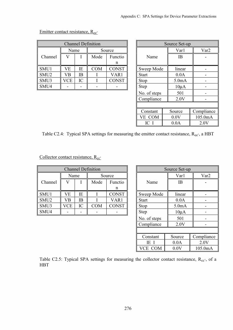
Appendix C: SPA Settings for Device Parameter Extractions
276
Emitter contact resistance, Ree’
Channel Definition Source Set-up Name Source Var1 Var2 Channel V I Mode Functio
n Name IB -
SMU1 VE IE COM CONST Sweep Mode linear - SMU2 VB IB I VAR1 Start 0.0A - SMU3 VCE IC I CONST Stop 5.0mA - SMU4 - - - - Step 10µA -
No. of steps 501 - Compliance 2.0V - Constant Source Compliance VE COM 0.0V 105.0mA IC I 0.0A 2.0V
Table C2.4: Typical SPA settings for measuring the emitter contact resistance, Ree’, a HBT Collector contact resistance, Rcc’
Channel Definition Source Set-up Name Source Var1 Var2 Channel V I Mode Functio
n Name IB -
SMU1 VE IE I CONST Sweep Mode linear - SMU2 VB IB I VAR1 Start 0.0A - SMU3 VCE IC COM CONST Stop 5.0mA - SMU4 - - - - Step 10µA -
No. of steps 501 - Compliance 2.0V - Constant Source Compliance IE I 0.0A 2.0V VCE COM 0.0V 105.0mA
Table C2.5: Typical SPA settings for measuring the collector contact resistance, Rcc’, of a HBT
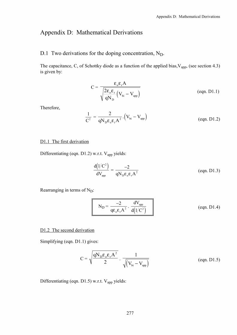
Appendix D: Mathematical Derivations
277
Appendix D: Mathematical Derivations D.1 Two derivations for the doping concentration, ND. The capacitance, C, of Schottky diode as a function of the applied bias,Vapp, (see section 4.3) is given by:
C = ( )
ε εε ε
o r
o r
Dbi app
A
qNV V2 −
(eqn. D1.1)
Therefore, 1
2C = ( )2
2qN AV V
D o rbi appε ε
. −
(eqn. D1.2)
D1.1 The first derivation Differentiating (eqn. D1.2) w.r.t. Vapp yields:
( )d CdVapp
1 2
= −22qN AD o rε ε
(eqn. D1.3)
Rearranging in terms of ND:
ND = −22q Ao rε ε
. ( )dV
d Capp
1 2
(eqn. D1.4)
D1.2 The second derivation Simplifying (eqn. D1.1) gives:
C = qN AD o rε ε 2
2.
( )1
V Vbi app−
(eqn. D1.5)
Differentiating (eqn. D1.5) w.r.t. Vapp yields:

Appendix D: Mathematical Derivations
278
dCdVapp
= qN AD o rε ε 2
2. ( )1
23 2
V Vbi app−
−
(eqn. D1.6)
But from (eqn. D1.5),
( )1
V Vbi app− or ( )V Vbi app−
−1 2 = C
qN AD o rε ε 2
2
(eqn. D1.7)
Hence, subsituting (eqn. D1.7) in (eqn. D1.6), we obtain:
dCdVapp
= qN AD o rε ε 2
2. 1
22
2
3
CqN AD o rε ε
= 12
C
qN AD o r
3
22
2ε ε
= CqN AD o r
3
2ε ε
(eqn. D1.8)
Rearranging in terms of ND:
ND = Cq Ao r
3
2ε ε dC
dVapp
−1
(eqn. D1.4)
D.2 Derivation of built-in potential at the base-emitter heterojunction, Vbi(B-E), of a HBT The analytical expression for Vbi(B-E) is given by:
Vbi(B-E) = EgB + ∆EC + kTq
ln N NN N
DE AB
cE vB
(eqn. D2.1)

Appendix D: Mathematical Derivations
279
which can be re-written as:
Vbi(B-E) = EgB + ∆EC + kTq
ln N Nn n
DE AB
iB iE
+ kT
q ln n n
N NiB iE
CE VB
(eqn. D2.2)
But recall that,
niB = N NcB vB . exp−
qEkT
gB
2
(eqn. D2.3)
and,
niE = N NcE vE . exp−
qEkT
gE
2
(eqn. D2.4)
Thus, the final term in (eqn. D2.2) can be expressed as:
kTq
ln n nN N
iB iE
CE VB
= kT
q ln ( )N N
N Nq
kTE EcB vE
cE vBgB gE.exp − +
2
= kT2q
ln N NN N
cB vE
cE vB
- ( )1
2E EgB gE+
(eqn. D2.5)
And therefore, (eqn. D2.2) can now be written as:
Vbi(B-E) = EgB + ∆EC + kT2q
ln N NN N
cB vE
cE vB
+ kT
q ln N N
n nDE AB
iB iE
- ( )1
2E EgB gE+
= E EgB gE−
2 + ∆EC + kT
2q ln N N
N NcB vE
cE vB
+ kT
q ln N N
n nDE AB
iB iE
(eqn. D2.6)
But since, EgE > EgB, and
∆Eg = EgE - EgB
- ∆Eg
2 =
E EgB gE−2
(eqn. D2.7)
Hence we obtain the desired expression for the Vbi of a heterojunction:
Vbi(B-E) = ∆EC - ∆Eg
2 + kT
q2 ln N N
N NcB vE
cE vB
+ kT
q ln N N
n nDE AB
iB iE
(eqn. D2.8)