stochastic adc with random u-quadratic distributed
TRANSCRIPT

STOCHASTIC ADC WITH RANDOM U-QUADRATIC
DISTRIBUTED REFERENCE VOLTAGES TO UNIFORMLY
DISTRIBUTE COMPARATORS TRIP POINTS
by
Mithun Ceekala
Submitted in partial fulfilment of the requirements
for the degree of Master of Applied Science
at
Dalhousie University
Halifax, Nova Scotia
April 2013
© Copyright by Mithun Ceekala, 2013

ii
DALHOUSIE UNIVERSITY
DEPARTMENT OF ELECTRICAL AND COMPUTER ENGINEERING
The undersigned hereby certify that they have read and recommend to the Faculty of
Graduate Studies for acceptance of a thesis entitled “STOCHASTIC ADC WITH
RANDOM U–QUADRATIC DISTRIBUTED REFERENCE VOLTAGES TO
UNIFORMLY DISTRIBUTE COMPARATORS TRIP POINTS” by Mithun Ceekala in
partial fulfilment of the requirements for the degree of Master of Applied Science.
Date: April 23, 2013
Co-Supervisors: _________________________________
_________________________________
Readers: _________________________________
_________________________________

iii
DALHOUSIE UNIVERSITY
DATE: April 23, 2013
AUTHOR: Mithun Ceekala
TITLE: STOCHASTIC ADC WITH RANDOM U–QUADRATIC DISTRIBUTED
REFERENCE VOLTAGES TO UNIFORMLY DISTRIBUTE
COMPARATORS TRIP POINTS
DEPARTMENT OR SCHOOL: Department of Electrical and Computer Engineering
DEGREE: MASc CONVOCATION: October YEAR: 2013
Permission is herewith granted to Dalhousie University to circulate and to copy for
non-commercial purposes, at its discretion, the above title upon the request of individuals
or institutions. I understand that my thesis will be electronically available to the public.
The author reserves other publication rights, and neither the thesis nor extensive extracts
from it may be printed or otherwise reproduced without the author’s written permission.
The author attests that permission has been obtained for the use of any copyrighted
material appearing in the thesis (other than the brief excerpts requiring only proper
acknowledgement in scholarly writing), and that all such use has been clearly
acknowledged.
_______________________________
Signature of Author

iv
To my parents Mr.Padmanabhareddy Ceekala and
Mrs.Prasanna kumari

v
TABLE OF CONTENTS
LIST OF TABLES vii
LIST OF FIGURES viii
ABSTRACT xi
LIST OF ABBREVIATIONS USED xii
ACKNOWLEDGEMENTS xiii
CHAPTER 1 INTRODUCTION 1
1.1 Motivation 1
1.2 Objective 3
1.3 Organization 4
CHAPTER 2 BASIC CONCEPTS AND TYPES OF ADC’S 5
2.1 Concepts 5
2.1.1 Stochastic process, INL and DNL 5
2.1.2 ENOB, Resolution AND Input Dynamic Range 6
2.1.3 PDF and CDF 6
2.1.4 Gaussian distribution 7
2.1.5 Uniform distribution and U-quadratic Distribution 8
2.2 Types of ADC’s 9
2.2.1 Flash ADC 9
2.2.1.1 Architecture 9
2.2.1.2 Limitations 11
2.2.2 Stochastic Flash ADC 13
2.2.2.1 Architecture 13
2.2.2.2 Limitations 16
2.2.3 Multiple Comparator Group Stochastic ADC 16
2.2.3.1 Architecture 16
2.2.3.2 Limitations 20
CHAPTER 3 STOCHASTIC ADC WITH RANDOM U-QUADRATIC DISTRIBUTED
REFERENCE VOLTAGES: CIRCUITS AND IMPLEMENTATIONS 21
3.1 Comparator 21
3.1.1 Dynamic Comparator 27
vi
3.1.2 S-R Latch 34
3.1.3 Offset extraction method 40
3.2 Proposed Architecture 44
3.3 Wallace Tree Adder 48
CHAPTER 4 REFERENCE SIGNAL GENERATION 53
4.1 Choosing PDF of Reference Signal 53
4.2 Reference Signal Generation Circuit 57
CHAPTER 5 RESULTS 60
5.1 System Level Simulation 60
5.2 Circuit Level Results 63
5.3 Comparision of Different Architectures 64
CHAPTER 6 FUTURE WORK AND CONCLUSION 67
APPENDIX 69
BIBLIOGRAPHY 76

vii
LIST OF TABLES
Table 1 S-R latch Input/Output Truth table ...................................................................... 35
Table 2 Input/Output of a Full adder ................................................................................ 50
Table 3 Comparison between the proposed stochastic ADC and the other different
architectures .................................................................................................... 66
Table 4 Code to generate reference values for system level results .................................. 69
Table 5 OCEAN Script code for extracting the trip points of comparator after
applying reference voltages in TSMC 90nm technology ................................ 70

viii
LIST OF FIGURES
Fig.1(a) Fig showing DNL .............................................................................................. 5
Fig.1(b) Fig showing INL ............................................................................................... 5
Fig.2 PDF of Gaussian distribution ............................................................................ 7
Fig.3 PDF of uniform distribution .............................................................................. 8
Fig.4 PDF of U-Quadratic distribution ....................................................................... 8
Fig.5 Block diagram of Conventional Flash ADC ................................................... 10
Fig.6 Block diagram of stochastic flash ADC .......................................................... 14
Fig.7(a) PDF of comparator internal offset ................................................................... 14
Fig.7(b) CDF of comparator internal offset .................................................................. 15
Fig.8(a) PDFs of comparator groups and resultant MCG ADC .................................... 17
Fig.8(b) CDFs of comparator groups and resultant MCG ADC ................................... 17
Fig.9 Block diagram of MCG ADC ......................................................................... 18
Fig.10 Block diagram of Pre-amplifier based comparator .......................................... 22
Fig.11 The Input/output characteristic of an ideal comparator ................................... 23
Fig.12 Positive feedback realization for a comparator using two inverters ................ 23
Fig.13 Input common mode voltages range for comparator ....................................... 25
Fig.14 Differential pair Dynamic comparator ............................................................ 28
Fig.15(a) output node Discharging phase ....................................................................... 29
Fig.15(b) output node Charging phase when the Vclk is high ........................................ 29
Fig.16 Time domain transition curve of a typical dynamic comparator ..................... 30
Fig.17 Resistor Divider or Lewis-Gray Dynamic comparator .................................... 31
Fig.18(a) Set latch configuration for an OR gate ............................................................ 34
Fig.18(b) Set latch redrawn ............................................................................................. 34
Fig.19 Reset latch configuration for an OR gate ........................................................ 34
Fig.20(a) S-R latch ........................................................................................................ 35

ix
Fig.20(b) Traditional view of S-R latch .......................................................................... 35
Fig.21 NAND S-R latch ............................................................................................. 36
Fig.22 Circuit diagram for an inverter ........................................................................ 37
Fig.23 Circuit diagram for a NOR gate ...................................................................... 38
Fig.24 Circuit diagram of an S-R latch with NOR gates ............................................ 38
Fig.25 Circuit diagram of the latch used in this work ................................................. 39
Fig.26 Block diagram of clocked comparator ............................................................ 40
Fig.27 Block diagram of DTOB ................................................................................. 41
Fig.28 DTOB Waveforms .......................................................................................... 42
Fig.29 DTOB practical implementation ..................................................................... 42
Fig.30 Probability distribution of 30000 comparators offset ...................................... 43
Fig.31 Figure showing the transformation of comparator trip points after
applying reference signal................................................................................. 45
Fig.32 Block diagram of the proposed architecture .................................................... 46
Fig.33 PDF of comparators trip points after applying reference signal ...................... 47
Fig.34 CDF of comparators trip points after applying reference signal ...................... 47
Fig.35 Block diagram of a full adder ........................................................................ 49
Fig.36 Block diagram of a Wallace tree adder used as a encoder for 3-Bit ADC ...... 50
Fig.37 PDF of reference signal with 30000 reference voltages .................................. 54
Fig.38 Graph showing the relation between σ and β .................................................. 56
Fig.39 h(x) for different values of β ........................................................................... 56
Fig.40 Circuit used for generating comparator reference voltages ............................. 57
Fig.41 Histogram of 1024 comparators trip point in the proposed design using
90nm CMOS technology ................................................................................ 58
Fig.42 Model implementation in Simulink ................................................................ 60
Fig. 43 PSD of proposed ADC system level simulation with SNDR and ENOB
included in the graph for ±400mV input dynamic range ................................ 61

x
Fig. 44 PSD of proposed ADC system level simulation with SNDR and ENOB
included in the graph for ±300mV input dynamic range ................................ 62
Fig. 45 PSD of the proposed ADC using 90nm CMOS technology with SNDR
and ENOB included in the graph for ±400mV input dynamic range ............. 63
Fig. 46 PSD of conventional Stochastic ADC with ENOB and SNDR included
in the graph ..................................................................................................... 64
Fig. 47 PSD of Multiple group Stochastic ADC with ENOB and SNDR included
in the graph ..................................................................................................... 64
Fig.48 PSD of conventional Flash ADC with ENOB and SNDR included in the
graph ............................................................................................................... 65

xi
ABSTRACT
This thesis presents a new architecture of stochastic Analog-to-Digital converter (ADC). A
standard Stochastic ADC uses comparator random offset as the trip point while all the
comparators have the same reference voltages. Since the offset of a basic comparator
depends on a number of independent random variables, the offset will follow randomly
distributed Gaussian function. The input dynamic range of this standard stochastic ADC is
±σ. For 90nm technology σ value is around 153mV. A technique is presented that converts
overall transfer function of a stochastic ADC i.e. Gaussian distribution into almost
uniformly distribution with a wider range. With the proposed technique, an input
dynamic range of ± 153mV and ENOB of 4bits of standard stochastic ADC are increased
to variable input dynamic range of ±250mV to ±500mV and ENOB of 6bits.

xii
LIST OF ABBREVIATIONS USED
DNL Differential Non-linearity
INL Integral Non-linearity
ENOB Effective number of bits
PDF Probability density function
CDF Cumulative distribution function
ADC Analog to digital converter
MCG ADC Multiple comparator Group ADC
SQNR
DOTB
Signal to quantization noise ratio
Dynamic offset test bench
CMRR
SNDR
CMOS
GND
PMF
ISI
NMOS
PMOS
VCVS
ROM
Common mode rejection ratio
Signal to noise and distortion ratio
Complementary Metal oxide semiconductor
Ground
probability mass function
Inter-Symbol Interference
n-type metal oxide semiconductor
p-type metal oxide semiconductor
voltage controlled voltage source
Read only memory

xiii
ACKNOWLEDGEMENTS
I owe my deepest gratitude to my supervisor Dr. Kamal El-Sankary and Co-supervisor
Dr. Ezz El-Masry for their valuable suggestions without which this work would be
incomplete. Their deep insight and extensive knowledge on analog circuit design were
very helpful to me. I also thank Dr. Jason Gu and Dr. William J. Phillips in my supervisory
committee.
I also extend my gratitude to all the group mates in the VLSI group for sharing their
knowledge and experience in analog IC design, to Mr. Mark Leblanc in particular for all
the technical support and troubleshooting of my software related issues. I also thank the
department staff Selina Cajolais and Nicole Smith for their support throughout my stay at
Dalhousie University and to enable my stay pleasant and remarkable.
I dedicate this to my beloved parents who stood by me through thick and thin and to
enable me to achieve this humble attempt.

1
CHAPTER 1 INTRODUCTION
This chapter introduces the thesis by providing the research motivations, objectives
and organization.
1.1 Motivations
In the modern world, there is a heavy demand for the portable devices operated
with batteries and it has been increasing day-by-day. The most important criteria for
these portable electronic devices are the operation at low power but with high speed and
resolution. The power consumption can only be reduced by decreasing the size of the
components used in the device.That is why there has been a drastic decrease in the size
of the technology from micrometer to nanometer scale. With the introduction of
integrated circuits, the world of electronics is completely revolutionized. For
fabricating Integrated circuits Complementary Metal oxide semiconductor (CMOS)
technology continues to be the dominant technology.In 1965 Intel co-founder Gordon
E. Moore observed and described in a paper that the number of transistors per chip will
double for every 18 to 24 months and this observation is now referred to as Moore’s law
[1]. Owing to the decrease in the size of the components used inside the device the
process variation and other non-idealities greatly affect the performance of the device.
The signals that occur naturally are analog (continuous in time and amplitude).But the
digital signals have the following advantages over the analog signals[2]
Precise signal level of digital signal is not vital, meaning that the digital signals
are fairly immune to imperfections that are caused by the electronic circuits
whereas analog signal are not.

2
In digital signal transmission, codes can be used for encryption and decryption
of data, error correction and error detection. These are not available in analog
signal transmission.
With greater immunity to noise, digital signals can convey information. This is
because the information is conveyed by the presence or absence of the data bit
whereas analog signals are affected by all levels of noise.
Bandwidth used for the digital signal transmission is less when compared to
analog signals which means that more information can be forced into the same
space.
Signals can be transmitted over a longer distance if digital signals are used.
Electromagnetic interferences for digital signals are low compared to analog
signals.
These advantages make the digital signals superior to analog signals but as mentioned
above, natural signals are analog signals. To utilize the advantages of digital signals all
analog signals that are received should be converted into a digital domain. This is where
analog to digital converters comes into play. One of the many challenges faced by the
analog designers is to design an ADC for high speed, high resolution and low power
consumption.

3
1.2 Objectives
Based on the above discussion, the thesis focuses on the design of an Analog to
digital converter(ADC) which uses comparators internal input offset with higher
resolution and variable input dynamic range. The following goals are aimed at and are
being achieved:
1 High speed
2 High resolution
3 Variable Input dynamic range
4 Increased active comparators
By using the proposed architecture,a resolution of 6.5 bits is achieved. Since this
architecture resembles FLASH ADC structure, its operating speed is almost the same as
that of FLASH ADC’s architecture. The input dynamic range of this architecture is
from ±250mV to ±500mV. The active comparators, that take part in the decision
making increased from 48% to 80% when compared to conventional stochastic Flash
ADC. As ADC plays an important role in the performance of any system, research
work is still going on in this field to improve the characteristics of stochastic ADC and
Flash ADC where speed plays a major role [27] [28].

4
1.3 Organization
The work stochastic ADC with random U-quadratic distributed reference
voltages to uniformly distribute comparator trip points [26] that has been realized
during this research is organized as follows.
In chapter 2 the basic concepts used in this work and the terminology used in
ADC’s are introduced. Later in this chapter,the different types of ADC architectures
and their limitations are discussed.
In Chapter 3, the proposed architecture is described.In addition to that, basic
building blocks used in the proposed design like comparator, R-S latch and Wallace
tree adder are discussed. Test bench used for extracting the offset of dynamic
comparators is also discussed in this chapter.
Chapter 4 describes the method to generate the reference signal and how to choose
the Probability density function (PDF) of the reference signal.
Chapter 5 focuses on the system level simulation and the circuit level simulation
results. This chapter also presents a comparison table between different architectures
and how the proposed one is better than the other Flash ADCs.
In chapter 6,the considerations for future works are discussed and thus it leads to
the Conclusion .

5
111
110
101
100011
010
001
000
Out
put
digi
tal c
ode
ADC output
Input signal
Input voltage
ADC output
Ideal ADC output
Input voltage
Dig
ital C
ode
In this chapter, the discussion will focus on the basic ADC’s architectures such as
Flash ADC, Stochastic ADC and Multiple group stochastic ADC. Also terminologies
used in ADC’s are discussed.
2.1 Concepts
2.1.1 Stochastic process, INL and DNL
Stochastic Process: It is the opposite of deterministic process and is defined as
collection of random variables defined on a common sample space [3]
DNL (Differential Non-Linearity): It is the difference between the input signal
(continuous amplitude and time signal) and the output of the built ADC (continuous
time discrete amplitude). This is also called Quantization Error[4]. The two signals of
the DNL are shown in Fig.1 (a)
INL (Integral Non-Linearity): It is the difference between the output of ideal ADC and
the output of the real ADC when both the outputs are converted to continuous time
discrete amplitude format [4]. The two signals of the INL are shown in Fig.1 (b)
Fig.1(a) Fig.1(b)
CHAPTER 2 BASIC CONCEPTS AND TYPES
OF ADC’s

6
2.1.2 ENOB, Resolution and Input dynamic range
ENOB (Effective Number of Bits): This is the number of bits used to represent the
analog signal into the digital format. If ENOB is denoted by N then there will be 2𝑁
quantization levels [5].
𝐸𝑁𝑂𝐵 =𝑆𝑁𝐷𝑅−1.76
6.02
Where SNDR is Signal to Noise and Distortion ratio
Resolution: It is the smallest change in the input signal that will change the output
digital code [4].
𝑄 =𝑉𝑝 − 𝑝
2𝑁
Where N is the ENOB and
Vp-p is the Vmax-Vmin voltage of the input signal
Input Dynamic Range: It is the input voltage range in which ADC works properly
without saturating at any voltage.
2.1.3 PDF and CDF
PDF (probability density function): Is defined as, the continuous random variable
representation over the relative distribution of frequency. From this function we can
derive parameters such as mean and variance. If an integral is considered in a particular
range then it gives the probability of the random variable to lie with that range. This can
also be called as frequency function. [6]

7
Std(2σ)
µx
f(x)
∫ 𝑓(𝑥)𝑑𝑥∞
−∞= 1. It means that the area under the probability density curve should
be one.
CDF (cumulative distribution function): is defined as, the integral or sum of the
probability density function. The property of CDF is it is always monotonically
increasing function i.e., if x1 and x2 are the two points of the CDF then F(x1) ≤ F(x2) if
x1 ≤ x2. [6]
2.1.4 Gaussian distribution
Gaussian distribution is also known as normal distribution or bell shaped curve.
Any random variable whose PDF follows the below pattern is said to be normally
distributed. The PDF will be symmetrical about the mean (µ). Fig.2 shows the PDF of
Gaussian distribution. [6]
f(x) =1
√2𝜋𝜎𝑒
−(𝑥−µ)2
2𝜎2
Where σ is the standard deviation of the random variable and µ is the mean of the
standard variable
Fig.2 PDF of Gaussian distribution
8
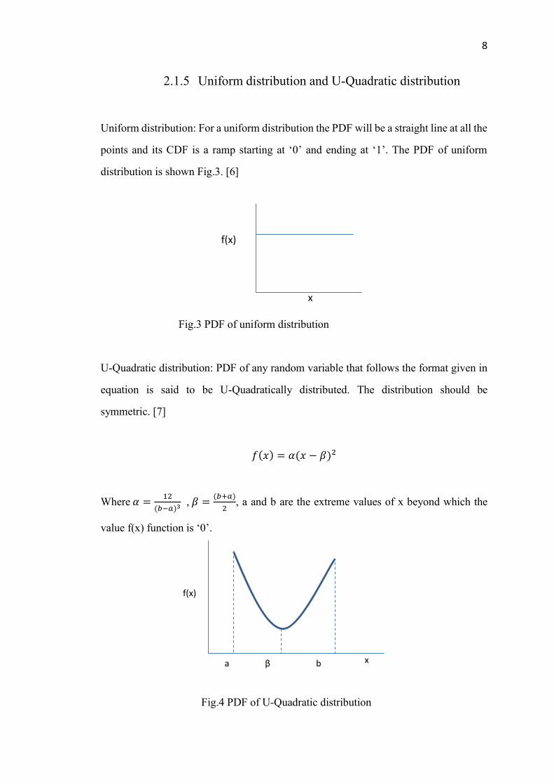
2.1.5 Uniform distribution and U-Quadratic distribution
Uniform distribution: For a uniform distribution the PDF will be a straight line at all the
points and its CDF is a ramp starting at ‘0’ and ending at ‘1’. The PDF of uniform
distribution is shown Fig.3. [6]
Fig.3 PDF of uniform distribution
U-Quadratic distribution: PDF of any random variable that follows the format given in
equation is said to be U-Quadratically distributed. The distribution should be
symmetric. [7]
𝑓(𝑥) = 𝛼(𝑥 − 𝛽)2
Where 𝛼 =12
(𝑏−𝑎)3 , 𝛽 =(𝑏+𝑎)
2, a and b are the extreme values of x beyond which the
value f(x) function is ‘0’.
Fig.4 PDF of U-Quadratic distribution
f(x)
x
a β b
f(x)
x

9
2.2 Types of ADCs
ADC is a circuit that converts continuous time and amplitude signal to discrete
time and amplitude signal. In theory we can get many types of ADCs, but in this work
we are concentrating mainly on the three types of ADCs
Flash ADC
Stochastic flash ADC
Multiple group stochastic ADC
Flash ADCs have the highest speed compared to any other ADC’s architectures in the
literature [4]. This is because all the comparators are given with reference voltages and
their output is converted to a digital code by thermometer code converter without any
delay. The proposed architecture resembles the Flash ADC structure and the main
goal of this architecture is that it should work with almost the same speed as that of
Flash ADC. So, this architecture is compared to the above three architectures.
2.2.1 Flash ADC
2.2.1.1 Architecture
In general conventional Flash ADC consists of three blocks:
Reference signal generator block
Comparators block
Conversion block
For N-bit ADC we need 2𝑁 − 1 number of comparators. Each comparator has two
terminals, one for the input signal and the other for the reference signal. If the input
signal voltage is greater than the reference signal voltage, the comparator will produce
a logic high voltage.

10
+
-
+
-
+
-
+
-
R/2
PRIORITY ENCODER
R/2
R
R
R
VDC
INPUT SIGNAL
volt
age
0.25
0
.5
0.7
5
1
Error in the level because of comparator offset or deviation of the resistor
from its ideal value
Error in resistance(±10%
tolerance)
Offset of the Comparator
Reference voltage for all the comparators are generated by a resistor ladder. The
resistor values in the resistor ladder should be precisely set such that the reference
voltages generated from this resistor ladder should equally place the comparators by
1LSB (Least Significant Bit).
The logic output of the comparator is given to a conversion block which is
generally a thermometer code conversion logic block or a priority encoder that converts
the logic high and low voltages to a digital code.
Fig.5 Block diagram of Conventional Flash ADC

11
2.2.1.2 Limitations
Limitations of Flash Analog to digital converter
Comparators offset.
Error in reference voltages.
Comparators offset:
Each comparator comes with offset. There are two types of comparators offset [8][12]
Static offset.
Dynamic offset.
Static offset is due to the mismatch in µCox (µ is the mobility of the charge carriers in
the transistor and Cox is the Gate oxide capacitance) and threshold voltage (Vth) of the
transistors. Dynamic offset is due to the parasitic capacitances formed and their
mismatch inside the comparator. Due to these reasons there is offset voltage inside a
comparator and no two comparators will have the same offset voltage. Because of the
offset voltage, comparator will switch before or after the desired voltage.
Error in reference voltages:
Reference voltages to comparators are set by using resistor ladder. In this resistor
ladder all the resistors should be of constant value but usually a resistor comes with a
tolerance of ±5%. Let’s consider that we are using a 1kΩ resistor to set a reference
voltage of 0.5V. The ±5% tolerance will cause resistor value after manufacturing to
vary between 950Ω-1050Ω. Due to this the reference voltage at the comparator input
reference terminal will be a different one, either less than or greater than the desired

12
value and making the ADC to switch at that particular voltage instead of the desired
one.
Due to the above limitations, comparators in the Flash ADC will switch before or after
the desired reference levels. The following example shows the effect of the two
limitations on the output digital code.
Let us consider
Input dynamic range =1V (p-p)
Number of bits = 3 bits
Resolution =1𝑉(𝑝−𝑝)
23−1 =
1
7𝑣
Comparators offset =120mV
Detecting digital code = “010”
If there is no comparator offset and error in the resistance value the reference voltage
should be 2
7v, but there is offset of 120mv which will make the comparator to see a
reference voltage of little bit greater than 3
7v at the reference terminal. So the
comparator will switch on that particular value and now the detected digital code will
be “011” instead of “010” and it is the same in case if there is any error in the reference
voltages value because of the tolerance in the resistance value.
One method of reducing the comparator’s offset is by increasing the size of the
transistors used in the comparator which will cost larger chip area. The other way of
reducing the comparator’s offset is with extra circuitry such as auto-zeroing and offset
storage techniques, but it will increase power consumption. Also, we cannot eliminate
the comparator’s offset completely and the circuits have to be designed to tolerate these
imperfections. Also, it is not possible to obtain accurate reference voltages at
comparators reference terminals, and hence stochastic flash ADC is proposed to
address the above two limitations.

13
2.2.2 Stochastic flash ADC
2.2.2.1 Architecture
In stochastic flash ADC the input signal is connected to all the comparators but the
threshold voltages of all the comparators are not precisely set. They are allowed to be
random by connecting all reference leads of the comparators to the same voltage level
usually ground (GND). The randomness of the comparators' threshold voltages is due
to the comparators' internal offset. With this arrangement the comparators will trip
based on their internal offset voltage, which means when the input voltage crosses the
internal offset voltage, then that particular comparator will be switched on. Block
diagram of stochastic flash ADC is shown in Fig.6 [9].
The central limit theorem of probability says that the sum of independently
distributed random variables with certain mean and finite variance approaches normal
distribution as the number of variables increases [10].
Comparator’s offset in this ADC is dependent on different factors such as mismatch
between the transistors, parasitic capacitances, variation in oxide thickness and variation
in the threshold voltages. Because of all these factors, the comparators' internal offset is
assumed to follow Gaussian distribution.
The comparator used in this work is implemented using 90nm CMOS
technology and has offset that follows Gaussian distribution with a standard deviation of
around 153mV. The output of the ADC follows the cumulative distribution of the
comparator's internal offset and hence when a ramp signal is applied, the voltage
transfer function of this ADC is nothing but the cumulative distribution function of the
Gaussian distribution function. The PDF and CDF of the internal offset are shown in the
Fig.7 (a) and 7(b) respectively.

14
Std =153mV
Input Voltage
No
Co
mp
arat
ors
Mean=0V
+
-
+
-
+
-
N-bits
no. c
ompa
rato
rs
input voltage(V) 3σ 2σ -σ 0 σ 2σ 3σ
linearity range
comparator trip points CDF
comparator offset PDF
no. c
ompa
rato
rs
voltage(v)
input signal
volta
ge(v
)
The PDF of the Gaussian distribution is almost uniformly distributed within the range
of ±σ (standard deviation). When the stochastic ADC is operated within the voltage
range of ±153mV, which is the standard deviation of the comparator’s internal offset
then the stochastic ADC transfer function will not be saturated. That means the input
dynamic range of this ADC is around ±153mV.
Fig.6 Block diagram of stochastic flash ADC
Fig.7 (a) PDF of comparator internal offset

15
No. comparators
Input voltage
Fig.7 (b) CDF of comparator internal offset
In case of normal flash ADC, the number of comparators required for N-bits of
quantization is 2𝑁 − 1.This is because the threshold voltages of the comparators are
assumed to be precisely set.However, in case of stochastic ADC, the comparators'
tripping points are random and consequently more than 2𝑁 − 1 comparators are
needed. The number of comparators required for N-bits of quantization is calculated
by assuming that the stochastic ADC comparator trip points are uniformly distributed
within the input dynamic rage and is given by the below equation:
𝑛 ≈ 2 ∗ 4𝑁
Where n is the number of active comparators (active comparators are comparators
whose offset+reference voltage is within the input dynamic range)
In this ADC the number of comparators should be increased by factor of 2, in order to
increase the accuracy by 1 bit.
Input dynamic range
±153mV

16
2.2.2.2 Limitations
The limitations of this architecture are
Input dynamic range
Number of active comparators
Not exactly uniformly distributed
The input dynamic range of this architecture is around ±153mV which is the
standard deviation of the designed comparator offset. Since the offset has Gaussian
distribution and is not uniformly distributed within the range of ±σ, applying input
voltage outside this range will cause nonlinearity.
The number of active comparators in the stochastic ADC is around 68%, which
mean that the remaining 32% of the comparators remains always on or off contributing
to more power consumption and offset error.
In the stochastic ADC it is assumed that all the comparators within the input
dynamic range are uniformly distributed but in reality they are not. This makes the
transfer function of the ADC to be slightly deviating and resulting in the decreasing of
number of quantization levels.
Results obtained by using this architecture is only 4.5 bit with 30000 comparators
within an input dynamic range of ±153mV (i.e. ±σ).
2.2.3 Multiple comparator group stochastic ADC (MCG ADC)
2.2.3.1 Architecture
In multiple comparator groups stochastic ADC the comparators are divided into
different groups where comparators in each group are connected to the same reference
voltage[11]. Just as in the case of stochastic ADC, the comparators in each group will

17
follow Gaussian distribution. By splitting the number of comparators in multiple
groups and connecting different reference voltages to those groups, multiple Gaussian
distributions are virtually created with same variance but with different means. The
mean of each comparator group is shifted by the same value as of the group’s reference
voltage. The PDF and CDF of the two groups ADC with each group’s PDF and CDF
mentioned in Fig.8 (a) and 8(b) respectively. The probability density function of the
resultant curve is almost uniformly distributed in the input dynamic range of ±153mV,
when this ADC is operated in this range, then this will give the maximum quantization
levels. To get maximum linearity, the reference voltages given to each comparator
group should be ±a(a=1.078σ, σ is the std of the comparators internal offset). This
makes the two Gaussian distribution curves means are placed 2.156σ apart. The block
diagram of the multiple comparator group stochastic ADC is shown in Fig.9.
Fig.8(a) PDFs of comparator groups and resultant MCG ADC
Fig.8(b) CDFs of comparator groups and resultant MCG ADC
0
0.2
0.4
0.6
0.8
1
-0.6 -0.36 -0.12 0.12 0.36 0.6
+a
-a
resultant
Input
voltage
CDF of comparators
-0.6 -0.36 -0.12 0.12 0.36 0.6
Pro
bab
ility
of
com
par
ato
rs
+a
-a
resultant
Input voltage

18
Comparator group I
Comparator group II
Input voltage (RAMP SIGNAL)
+a
-a
comparator offset PDF
no
. co
mp
arat
ors
voltage(v)+a
comparator offset PDF
no
. co
mp
arat
ors
voltage(v)-a
N-bits
In the MCG ADC, the distribution of comparators within the input dynamic range is
almost uniformly distributed and its PMF (probability mass function) can be represented
by a binomial distribution:
PMFK(n, v) = (𝑛𝑘
)𝑣𝑘(1 − 𝑣)𝑛−𝑘
Fig.9Block diagram of MCG ADC
For simplicity, the input range is considered as 0 to 1 and n comparators lie within this
range. If k is the number of comparator thresholds lie within any arbitrary point v and 0,
then the number of thresholds lie within v to 1 is (n-k).
LSB is considered as 1/n in order to bound quantization to zero at the extremes of the
input and if any given value of the input, the output is merely k/n. The mean of the

19
output k/n as a function of v is given by the formula
Mean (𝑘
𝑛(𝑣)) = 𝑣
As a result in the range of 0 to 50% of the full-scale, there will be 50% of total
comparator thresholds will present. Any variation from this mean will cause
quantization error. If the variance is calculated then
Var (𝑘
𝑛(𝑣)) =
𝑣−𝑣2
𝑛
Noise power can be calculated by the formula
𝑃𝑛𝑜𝑖𝑠𝑒 = ∫ 𝑉𝑎𝑟(𝑘
𝑛(𝑣))
1
0
𝑑𝑣
Pnoise=1
6𝑛
𝑆𝑄𝑁𝑅 =√𝑠𝑖𝑔𝑛𝑎𝑙 𝑝𝑜𝑤𝑒𝑟
√𝑛𝑜𝑖𝑠𝑒 𝑝𝑜𝑤𝑒𝑟
𝑆𝑄𝑁𝑅 =
√1
12
√1
6𝑛
= √𝑛
2
From the above equation, we can calculate the number of active comparators required
to give the desired number of output quantization levels.
𝑁 = log2 √𝑛
2
Where N is the ENOB and n is the number of active comparators

20
In this architecture we can achieve ENOB of 6 bit with 30,000 comparators within the
input dynamic range of ±153mV.
2.2.3.2 Limitations
There are two limitations in this architecture
Number of active comparators
Input dynamic range.
Even by splitting the comparators into two groups, the active comparators still
remains 48% and the remaining 52% of the comparators will be either switched on or
switch off, all the time.
Input dynamic range of this architecture is not changed and it still remains
±153mV. Results obtained by using this architecture is only 6 bit with 30000
comparators within an input dynamic range of ±153mV (i.e. ±σ).

21
In this chapter, stochastic ADC with uniformly distributed comparator trip points is
proposed. Also comparator, Wallace tree adder used as a building block for this ADC is
presented.
3.1 Comparator
Flash ADC’s are the highest speed comparators available in the literature. Their
speed depends only on comparators and the conversion circuit used. There are two
kinds of comparators
Static comparator
Dynamic comparator
Static comparators will make decision based on the input signals and the output will be
updated whenever inputs are updated. As this comparator continuously looks for the
change, power dissipation will be high.
Dynamic comparators makes decision at certain instances (clock signal). Due to this,
the power dissipation is less. Dynamic comparators have higher accuracy as they
employ a strong positive feedback in a regenerative phase and have a reset phase. Static
comparators accuracy is lower as they don’t have a reset phase to employ strong
positive feedback. Typical dynamic comparators use a pair of cross coupled inverter
latches, connected back to back and positive feedback, in order to convert a small input
CHAPTER 3 STOCHASTIC ADC WITH
RANDOM U-QUADRATIC DISTRIBUTED
REFERENCE VOLTAGES: CIRCUITS AND
IMPLEMENTATIONS

22
difference to a digital level in a short period. Dynamic comparators suffer from large
offset but with a high speed, that is the reason why, they are used in flash ADC.
Dynamic comparators offset which is called as input-referred offset voltage is due to
mismatches such as threshold voltage Vth, current factor β(=µCox W/L), Parasitic
capacitances and mismatched output load capacitances. If large devices are used in
latching stage, a less mismatch can be achieved with a price of increased delay and
power.
To reduce the offset voltage, a preamplifier is used prior to the regenerative
output-latch. This architecture is named as preamplifier based comparator and its block
diagram is shown in Fig.10. The advantage of preamplifier prior to regenerative
output-latch is to amplify a small input voltage to a large one which will overcome the
offset voltage of the comparator. Also another advantage of this architecture is to
reduce the kickback noise from the switches used in the latch comparator. The
disadvantage of this pre-amplifier based comparator is the large static power
consumption.To overcome this drawback, dynamic comparators are used which will
have lower power consumption compared to pre-amplifier based comparators. The
reason for this is that the dynamic comparators will take decision once every clock
period and the remaining time they will be turned off.
Fig.10Block diagram of Pre-amplifier based comparator
Av Regenerative
Latch
S-R
Latch
Q
Q
Vin+
Vin-
Pre-amplifier

23
Vin
Vref
VoutVo
ut
Vin-Vref0V
VrefVin
Design considerations of voltage comparators are [13]
High gain
High speed
Accuracy
Wide input common mode range
CMRR (common mode rejection ratio)
Low power consumption
Small area
Low input capacitance
Fig.11The Input/output characteristic of an ideal comparator
For an ideal comparator, input/output Characteristic is shown in Fig 11. The
comparator's first requirement is that it should have a high gain (infinite gain) and that
is virtually obtained by positive feedback. The positive feedback can be obtained by
connecting two inverters back to back as show in Fig .12.
Fig.12 Positive feedback realization for a comparator using two inverters

24
High sampling rate is the second requirement of a comparator. Now-a-days all
the synchronous systems are working with higher speeds and the comparators should
work with higher sampling rate if it needs to work perfectly with the system. Latched
comparator operates using two non-overlap clock phases: one is evaluation phase and
the other is the rest phase. In an evaluation phase the comparator will compare the two
inputs and take a decision, positive feedback is enabled in this phase. In the reset phase,
comparator will clear its previous sample and the positive feedback is disabled. For fast
operation of the comparator, the reset phase should be completed quickly and
evaluation phase’s positive feedback should be enabled with a short regeneration time
constant.
High accuracy is the third requirement for a comparator. The factors that are
affecting the accuracy are: offsets, noise and residual value from the prior comparison.
Offset is the main contributor for the inaccuracy and it is classified into two types
systematic offset and random offset. Systematic offset can be minimized by designing a
symmetric circuit and by taking extra care in the layout process. Random offset is
caused by component mismatches in the layout and its variance is inversely
proportional to the 𝑊
𝐿 ratios of the transistors. So, in order to reduce random offset,
bigger transistors are usually used. Second factor that causes inaccuracy is the noise
including thermal noise, flicker noise, supply noise and sampling noise. Thermal noise
is white Gaussian noise due to increase in temperature of the device which in turn
creates more electron and hole pairs. Flicker noise is low frequency noise of a transistor.
Supply noise does not affect the output directly but it may change the input offset
momentarily. Sampling noise is caused by the fast transition of the clock signal from
reset to evaluation phase. If the sampling occurs at higher speed, then the sampling
noise can be neglected. The final factor causing comparator inaccuracy is the residual
value from the prior comparison. When the reset is not completed before the start of the
evaluation phase, an even small residual charge can generate a large error at the output.
Since the comparator is operating in positive feedback mode, the residual charge will

25
Vin
Vref
Vout
VDD
VSS
VICMR_MAX
VICMR_MIN
get exponentially increased. This residual charge mainly depends on the previous
sample and it is sometimes called as Inter-Symbol Interference (ISI).
A Comparator’s fourth requirement is wide input common mode range. Input
common mode range is defined as how close the inputs can be operated to the either
power supply rail while still maintaining good operation from the comparator.
VICMR_MAX, VICMR_MIN are shown in Fig. 13.
VICMR=VICMR_MAX - VICMR_MIN
VICMR_MIN = limited relative to VDD ( positive supply voltage)
VICMR_MAX = limited relative to VSS ( negative supply voltage)
Fig.13Input common mode voltages range for comparator
A Comparator’s fifth requirement is common mode rejection ratio (CMRR). It
is defined as the device's ability to reject the input signals common to both the input
terminals. A high CMRR is required in applications where a small voltage fluctuation
superimposed on a large offset is considered for the decision making.

26
A Comparator's sixth requirement is low power consumption. This requirement
is more pronounced in conventional flash ADC where 2𝑁 comparators are used in
parallel to design an N-bit resolution. If the power consumption of a single comparator
is not low, then the total power required for the complete circuit will be too high. For a
flash ADC, the power consumption doubles as the resolution increases by one bit. This
is because, for the increase in one bit resolution, the number of comparators should be
doubled.
Another requirement for a comparator is low input capacitance. Large input
capacitance will limit the bandwidth of the input signal. Similar to the power
consumption, the total input capacitance of Flash ADC is 2𝑁 times the input
capacitance of the comparator used. The input capacitance of the comparator depends
on the input differential pair transistors and hence the latter should be small in size to
lower the input capacitance at the expense of an increased offset voltage.

27
3.1.1 Dynamic Comparator
In literature we can find different types of dynamic comparators. The most widely used
dynamic comparators are
Differential pair dynamic comparators
Resistor divider or Lewis-Gray structure
The offset of these dynamic comparators typically vary between 70mV and 300mV.
The operation of the dynamic comparators depends on the sensing of the difference
between the two symmetric halves of the circuit. The latter arises due to the difference
in the input voltages or random mismatch between them. The difference between the
input voltages of the matched and mismatched cases is referred to the comparator’s
in-out as input referred offset voltage. This input referred offset voltage is one of the
key characteristics of the comparator.
3.1.1.1 Differential Pair Dynamic Comparator
This architecture contains two sets of differential pair with inverter latch at the
top which are cross coupled [15]. The decision is taken based on the currents that are
flowing through the inverters which is in-turn related to the inputs and the clock
voltage. At the initial stage, before applying clock signal Vout+ and Vout- voltages are
reset to VDD. When the clock signal is applied (i.e. Vclk= VDD), the comparator is
said to be in decision making phase and both the output nodes start discharging based
on the NMOS transistor currents of the inverters as shown in Fig.15(a). These
currents are related to the input voltages applied to the differential input pairs and their
tail currents. Due to the difference in NMOS pull down currents, one of the output
nodes crosses the falls beyond the threshold voltage of the PMOS transistor in the
inverter pair making that transistor to turn ON. As a result the other output node will
again charge to VDD as shown in Fig 15(b). This in turn will make the first output

28
Vin+ Vin- Vref- Vref+
Vout- Vout+
VDD
VSS
VclkVclk
M1M2
M5 M6
M4
M7M8
M10
M11 M12
Vclk
VclkM3 Vclk
M9
Vclk
VSS
VclkM13 M14
node to be pulled to VSS even faster. This operation is basically a positive feedback.
The transistors M3 and M9 increases the time of operation of input transistors in
saturation region during the evaluation phase (from reset phase to just before the start
of the evaluation phase, transistors M3 and M9 are switched on and these transistors
will drag the voltage at the source terminals of transistors M4 and M10 to VDD if the
transistors M3 and M9 are not present then they are not necessarily to be VDD at the
beginning of the evaluation phase. Due to this the VDS voltages of the input pair is
more and which in turn keep the transistors in saturation region for more time during
evaluation phase) and this will increase the amplification compared to resistor divider
dynamic comparator.
Fig.14Differential pair Dynamic comparator

29
Vout-Vout+
VDD
VSS
CLoad
IDiff-Pair
M2
M4CLoad
VDD
Vout-Vout+
VSSIDiff-Pair
M2
M4
(a) (b)
Fig.15 output node (a) Discharging phase (b) Charging phase when the Vclk is high
A typical time domain transmission curve for output is shown in Fig 16; the starting
point in the graph shows the discharging phase for both the outputs initially. Once, one
of the outputs drops faster than the other output, then the two outputs split (e.g. as
shown in the figures Vout- is dropped faster than the Vout+). The discharging phase of
the output nodes depends on inputs and the differential pair tail currents, once one of
the outputs drops faster than the other one at this point, the output nodes depends on
the PMOS sizing of the inverter. For a faster decision, the latch should have a stronger
PMOS pull-up. The trip point of the latch can be changed by changing the sizes of the
input transistors or by changing the reference voltage applied to the latch reference
terminal

30
Vout+
Vout-
Ou
tpu
tsTime
Fig.16 Time domain transition curve of a typical dynamic comparator
The drawbacks in this structure are:
When the clock signal is high, the tail current goes into the linear region and it
depends on the inputs of the differential pair. If any mismatches or any kind of
non-idealities are present, then the tail currents flowing through the two
inverters will not be the same and the latch offset will be substantial.
If the difference between the two inputs of the differential pair is large, then it
will turn off one of the transistors in the differential pair and the total tail
current will steers into the other transistor and hence the comparator will
compare only Vin+ with Vref+ (or Vin- with Vref-) rather than comparing the
differential voltages.

31
Vin+ Vref- Vin- Vref+
Vout+ Vout-
VDD
VSS
Vclk Vclk
M1M2
M3
M5 M6
M4
M7M8
M9
M10
M11 M12
V1 V2
3.1.1.2 Lewis Gray Dynamic Comparator
Fig.17 Resistor Divider or Lewis-Gray Dynamic comparator
In the Lewis-Gray structure comparator [14], the input transistors M5, M6, M11 and
M12 are operating in the triode region. In the triode region transistor acts as voltage
controlled resistor. To understand the functionality of this comparator, consider the
above voltage controlled resistor with ideal components with Vin+=Vref-, and
Vin-=Vref+, Vout+=Vout- with the cross coupled branches are broken. Then the two
sub-circuits consisting of transistors M1 to M6 and M7 to M12 will be identical. The
line in the above circuit, which divides the circuit into two sub-circuits is considered to
be the axis of cross symmetry for the circuit.
Since in triode region, transistor acts as a voltage controlled resistor when there is any
small change in the input voltage, then there will be a large change in the resistance of
the transistor. Because of this reason, resistor Lewis-Gray dynamic comparator suffers
from large offset. The advantages of this structure are less power consumption (no

32
static power consumption) and adjustable threshold voltage (decision level)
𝑉𝑖𝑛(𝑡ℎ𝑟𝑒𝑠ℎ𝑜𝑙𝑑) =𝑊(𝐴)
𝑊(𝐵)∗ 𝑉𝑟𝑒𝑓
Where WA=W6=W12
WB=W5=W11
Vin= (Vin+)-(Vin-)
Vref= (Vref+)-(Vref-)
Operation of Lewis-Gray Dynamic Comparator:
When Vclk is low, the comparator is said to be working in reset phase. In this
phase the PMOS transistors M1 and M8, called reset transistors, will charge the Out
nodes Vout+ and Vout- to VDD and the voltage across the drains of the transistors M5,
M6, M11 and M12 are discharged to ground while NMOS transistors M4 and M10 are
turned off.
When Vclk is high the comparator is said to be working in decision making
phase, the node voltages V1 and V2 in the Fig.17 are given by the equations
𝑉1 =𝑟𝑑𝑠𝑜𝑛(𝑀5‖𝑀6)
𝑟𝑑𝑠𝑜𝑛(𝑀5‖𝑀6) + 𝑟𝑑𝑠𝑜𝑛(𝑀3) + 𝑟𝑑𝑠𝑜𝑛(𝑀4)∗ 𝑉𝑜𝑢𝑡 −
𝑉2 =𝑟𝑑𝑠𝑜𝑛(𝑀11‖𝑀12)
𝑟𝑑𝑠𝑜𝑛(𝑀11‖𝑀12) + 𝑟𝑑𝑠𝑜𝑛(𝑀9) + 𝑟𝑑𝑠𝑜𝑛(𝑀10)∗ 𝑉𝑜𝑢𝑡 +
When the differential voltage across the transistors M5 and M6 increases then
voltage at node V1 decreases and this causes the voltage VGS4 to increase which in turn
increases Id4.This increase in Id4 decreases Vout-. This voltage is connected to the input

33
of the transistor M10 which will decrease the voltage VGS10 and this will allow Vout+
to increase. Due to the cross coupled inverter pair with positive feedback one output
node will discharge to ground and the other output node will charge to VDD.
The transconductance of transistors M4 and M10 is much higher than that of
the input pair; because of this differential voltage gain built between M4, M10 source
terminals from input transistor pair is not big enough to overcome the offset voltage
caused by even a small mismatch between transistor pair M4 and M10. Due to this
high transconductance M4 and M10 plays an important role in the decision making
and this transistors needed to be chosen or selected big enough such that offset voltage
is minimized but at the cost of increased power consumption. Besides those
transistors, transistors M3 and M9 mismatch will also contribute to the offset. As the
common mode voltage of the input transistor pair increases, the relative difference
between the voltage controlled resistors becomes smaller even with the same amount
of input voltage difference which in-turn increases the offset voltage.
To conclude from the above statements, it can be said that Lewis-Gray structure
has an advantage of zero static power dissipation but it has more disadvantages such as
high offset voltage and high dependence of offset voltage on common mode voltage.
So this type of comparator can be used for low resolution comparison.

34
S
Q
R
S
3.1.2 S-R Latch
Latch is a circuit that transfers from one state to another state when signaled and
remains in that state insensitive to input status until signaled again [16] [17]. For an
OR gate if any one of the inputs is high, then the output will be high. When OR gate's
output is connected to one of the inputs as shown in Fig.18(a), then the output will be
logic high. If the other input is changed to high, it will stay in that state permanently
even if any change in the input of the OR gate. The set latch shown is Fig.18 (a) can be
redrawn as shown in Fig.18(b) . This state is said to be set latch state because the latch is
set only once.
(a) (b)
Fig.18 (a) Set latch configuration for an OR gate (b) Set latch redrawn
The Fig.19 shows a reset latch configuration using a NOR and NOT gates. If the
output of the NOR gate is logic high at the initial state, both the inputs are connected to
logic low and the NOT gate will feedback logic low signal, yielding a stable condition.
When a logic high voltage is connected to the input terminal R, then the output of the
NOR gate produces a logic low signal and force the feedback signal to logic high. This
will force the output Q to a logic low and stay in that state permanently, independent of
the other input R and that is the reason why it is called the reset latch configuration.
Fig.19 Reset latch configuration for an OR gate

35
S
R
Q
QSQ
Q
R
If set latch and reset latch configurations are used separately, then it is of no use
because the circuit will stay in one state- either logic low or high permanently. When
set latch and reset latch configurations are used simultaneously in one circuit, then it is
possible to set the latch and reset the latch when ever needed. This configuration is said
to be S-R latch and is shown in Fig 20. If NOT gate in the Set latch shown in Fig.18 (b)
is replaced by a NOR gate, the device still operates as a Set latch and this input to the
Set latch is a function of the Reset pin from the Reset latch configuration. This is how
a Set-Reset latch is drawn from two 2- inputs NOR gates and Table 1 shows the
input/output truth table for S-R latch.
(a) (b)
Fig.20 (a) S-R latch (b) Traditional view of S-R latch
Table1 S-R latch Input/output truth table
S
R
Q
Q
Function
0 0 Q Q Storage state
0 1 0 1 Reset
1 0 1 0 Set
1 1 X X Undetermined state

36
S
R
Q
Q
1
2
S-R latch can also be produced from NAND gates with the same functionality
as of one produced from NOR gates and is show in Fig 21. For a NAND gate if any
one of the inputs is logic low then its output is logic high. When both the inputs Set
and Reset are logic low, then the output of NAND gates are shown below
NAND gate 1: 𝑆 ∙ = 1 ∙ = =𝑄
NAND gate 2:𝑅 ∙ 𝑄 = 1 ∙ 𝑄 =𝑄
Fig.21 NAND S-R latch
If either one of the inputs S or R is active high, while the other maintained at any logic,
this will set the respectively NAND gates output to logic high as explained below
NAND gate 1 (S=1) : 𝑆 ∙ = 0 ∙ =0 =1
Or
NAND gate 2 (R=1) :𝑅 ∙ 𝑄 = 0 ∙ 𝑄 = 0= 1
The logic high in the output of active NAND gate forces the other NAND gates output
to logic low.

37
VDD
VSS
Vin Vout
NAND gate 2 (S=1, R=0) :𝑅 ∙ 𝑄 = 0 ∙ 1 = 1 ∙ 1= 1=0
Or
NAND gate 1 (S=0, R=1) : 𝑆 ∙ = 0 ∙ 1 =1 ∙ 1 =1=0
Inverter can be designed with one PMOS and one NMOS connected as shown in
Fig 22 [19]. When Vin is high, the PMOS transistor will turn off and NMOS transistor
will turn on, connecting the output to VSS and now the output of the circuit is logic
low.When Vin low (VSS), the PMOS transistor will turn on and NMOS transistor will
turn off, connecting the output to VDD and now the output of the circuit will be
charged logic high.
Fig.22 Circuit diagram for an inverter
NOR gate can be implemented by two PMOS and two NMOS connected as
shown in Fig 23 [18]. When both the inputs Inp1 and Inp2 are active low, the output,
pin Out is connected to VDD and the output is charged to VDD. In the other cases
when either input or both are active high, the output terminal is disconnected for the
VDD terminal and connected to VSS terminal. The S-R latch circuit is shown in Fig 24
using NOR gates [20].

38
VDD
VSS
Inp1Inp2
Out
VDD
VSS
VDD
VSS
R S
Fig.23 Circuit diagram for a NOR gate
Fig.24 Circuit diagram of an S-R latch with NOR gates
In this circuit, two inverters are connected to the two input terminals of the S-R
latch as shown in Fig.25. This is because, for comparator used in this work in the reset
phase, the output of the comparator is charged to VDD which is logic high. This will
make the inputs S and R connected to logic high. In Table 1 if both the inputs are logic
high, then it will lead to an undetermined state. In order to get rid of this undetermined
state, the circuit shown in Fig 25 is used as a latch for the output of the comparator.

39
VDD
VSS
VDD
VSS
VDD
VSS
VDD
VSS
Out+Out-
Fig.25 Circuit diagram of the latch used in this work
In the reset phase of the comparator, the output nodes- Out+ and Out-, both are
charged to VDD. Because of these nodes, connected to the inverters as shown in Fig
25, VSS voltages will appear at the NOR gates of the S-R latch. As mentioned in
Table I, when both the Set and Reset inputs are given active low voltages, then the
latch will be in storage mode. It means that, whatever the voltages seen at the previous
decision making phase of the comparator is still prevailed.
In the decision making phase of the comparator, when the input voltage is greater
than the reference voltage, Out+ node will be discharged to VSS and Out- node will be
charged to VDD. When this is applied to the circuit shown in Fig 25, output node Q
will be charged to VDD and will be discharged to VSS and these voltages will stay
until the reference voltage becomes greater than the input voltage. When the reference
voltage becomes greater than the input voltage, their voltages will be reversed.

40
S-R Latch
S
R
Q
Q
+
-
Vin
Vref
Vclk
3.1.3 Offset Extraction Method
The block diagram of a clocked comparator is shown in the Fig 26.
Fig.26 Block diagram of clocked comparator
If the comparator is ideal, then the input referred internal offset should be ‘0’
that is if (Vin-Vref) > 0, the output is logic High and when (Vin-Vref) < 0, the output
logic should be Low. Due to component mismatches and other non-idealities, the
decision threshold shift away from zero and the amount by which the decision
threshold shifts is referred to as input referred internal offset of the comparator. The
test bench shown Fig 27 [21] calculates the input referred internal offset voltage of a
clocked comparator in a single run. This test bench uses all ideal components except
the comparator, for which the offset is to be calculated and this test bench is called
“dynamic offset test bench” (DOTB). This technique includes offset caused by static
mismatch and dynamic mismatch and when these results combined with statistical
techniques such as Monte Carlo simulations, the standard deviation of the offset can be
viewed.
41
S-R Latch
S
R
Q
Q
+
-
Vref
VFB
Vclk
Integrator 1
+
-VOD
Comparator under test
Fig.27 Block diagram of DTOB
The comparator, for which the offset voltage is to be calculated, is enclosed in a
negative feedback loop, containing an integrator. To maintain symmetry in the signal,
VOD an ideal differential amplifier is used so that VOD = 𝑄 − . The negative feedback
loop shown in the Fig.27 will have infinite DC gain and this is due to the integrator
and this ensures that whenever the system is in equilibrium state, the average value of
the signal VOD will be zero. In the equilibrium condition Vref–VFB , the average value is
equal to the decision threshold of the comparator and voltage waveforms at the
equilibrium condition are shown in Fig.28. In this test bench, the comparator output
alters between one and zero and after each comparison, the input of the comparator
slews across the decision threshold. The output of the test bench is a triangular
waveform (Vref–VFB) and it is easy to calculate the average which is nothing but the
input referred internal offset of the comparator.
42
Vclk
VOD
0V
Vref
VFB time
VCM
Vref
RCM
RCM
RCM
RCM
VFB
RS
RS
RS
RS
+
-
+
-
Q
Q
+
-
1
S1
S2
R1
R2
Gm
+
-
VINT
Fig.28 DTOB Waveforms
Fig.29 DTOB practical implementation
Practical implementation of this DTOB structure is shown in the Fig.29.
Comparator takes the decision based on the two differential inputs and among the two,
one is typically a reference signal. Comparator inputs are biased to a common mode
voltage by the voltage source VCM and the resistors RCM. The source resistances of the
circuits driving the comparator are modeled using the resistors RS and the ideal buffer
is used to convert the comparators output 𝑄 𝑎𝑛𝑑 to the single ended signal with

43
0
50
100
150
200
250
300
350
400
-0.6
-0.5
4
-0.4
8
-0.4
2
-0.3
6
-0.3
-0.2
4
-0.1
8
-0.1
2
-0.0
6
5.2
73
56
E-1
6
0.0
6
0.1
2
0.1
8
0.2
4
0.3
0.3
6
0.4
2
0.4
8
0.5
4
0.6
No
Co
mp
ara
tors
INPUT VOLTAGE
zero at the equilibrium state. This ideal buffer is followed by a resistive divider
which provides an attenuation when gear shift is implemented. The gear shift
technique lowers the gain of integrator when an equilibrium condition is reached and
this technique is used in this test bench, to reduce the peak to peak variation in VFB
signal so that the test bench will have greater accuracy. Initially, the switch S2 is
opened and whenever the desired value is obtained it is closed to reduce the loop gain.
The integrator block is built by using a transconductance cell and a capacitor. Initially
the switch S1 is closed to reset the integrator output. Once, the charge across the
capacitor is 0v, it is opened all the time to store the offset. The single ended integrator
output is converted to a differential input by using the voltage controlled voltage
source (VCVS), which is connected to the differential input of the comparator. The
polarity of the VCVS should be inverted, since this system is working in the negative
feedback mode. The input offset voltage of the comparator is given by Vref+VINT when
VCVS has unit gain.
Offset of the Lewis-Gray dynamic comparator extracted from test bench shown in
Fig.29 combined with statistical technique (Monte Carlo analysis) is shown in Fig.30.
The offset of the Lewis-Gray dynamic comparator will have probability density
function of Gaussian distribution with mean of 0V and standard deviation of 153mV.
Fig.30 Probability distribution of 30000 comparators offset

44
3.2 Proposed Architecture
Comparator is the basic building block for an analog to digital converter.
In this proposed design, Lewis-Gray dynamic comparator is used. In the stochastic
ADC, comparator trip points are based on the comparator internal offset and input
dynamic range depends on the standard deviation of the internal offset, to have a
higher input dynamic range, comparator with a higher standard deviation of the offset
is required. Due to this the reason Lewis-Gray dynamic comparator structure is chosen.
Stochastic ADC has limitations of smaller input dynamic range, smaller
percentage of active comparators and smaller ENOB. With Multiple groups stochastic
ADC a better ENOB can be achieved but the remaining two limitations cannot be
eliminated. With this proposed architecture, even the other two limitations can be
overcome to certain extent and also this architecture can be used for a variable input
dynamic range with the same ENOB, without modifying the hardware.
As shown in Fig.30, PDF of comparators internal offset follows a Gaussian
distribution and when a ramp input signal is given to a stochastic ADC whose
comparator trip points are based on the internal offset voltages of the comparators, then
number of switched on comparators will follow CDF (cumulative distribution function)
of the Gaussian distribution. This can be called as the transfer function of the
stochastic ADC. If observed at the CDF of the Gaussian distribution curve, it is almost
linear within the range ±σ (standard deviation of the internal offset).
The proposed design is based on a theorem in probability that, the resultant of
the sum of two or more independent random variables is the convolution of PDF’s of
random variables. When a reference signal is applied to the stochastic ADC, this
reference signal is considered as the second random variable and the comparators
internal offset is considered as the first, trip points of the comparators will follow a
distribution which is the convolution of PDFs of the reference voltage and the

45
PDF of comparator offset
PDF of reference voltages
PDF of comparator trip points
=*N
o c
om
par
ato
rs
No
co
mp
arat
ors
No
co
mp
arat
ors
Input voltage Input voltageInput voltage
comparator internal offset. Reference signal voltages PDF plays an important role in
the transfer function of the ADC. In the process of choosing the reference signal, it is
found that if a U-quadratic signal with certain mean and standard deviation provides
with maximum linearity compared to the other distributions and it is shown in Fig.31.
Fig.31Figure showing the transformation of comparator trip points after applying
reference signal.
The architecture of the proposed ADC is show in Fig.32. In the block diagram,
circles at the reference terminal of the comparator represents comparator’s internal
offset and when reference voltages which follows probability density function of
U-quadratic distribution are applied to the comparators reference terminals,
comparators trip points will be rearranged. This rearranged comparators trip points will
now have uniformly distributed probability density function within the input dynamic
range. The distribution of comparators trip points after applying reference voltages in
TSMC 90nm technology is shown in Fig.33 and the cumulative distribution of this
comparator trip points is shown in Fig.34.From the graph in Fig.34, it can be seen that
it is almost linear within the range -400mV to 400mV and also 80% of the comparators
are within this range. This increases the ENOB, without increasing the number of
comparators. This architecture needs only 30000 comparators to get 6.5 bit resolution
but stochastic ADC architecture needs more than 50000 comparators and multiple
group stochastic ADC needs around 35000 comparators. This architecture works for
±250mV to ±500mV but all the other architectures works for ±153mV.

46
+
-
+
-
+
-
N-bits
no
. co
mp
arat
ors
input voltage(V)-0.4 0.4
linearity range
comparator trip points CDF
reference signal PDF
no
. co
mp
arat
ors
voltage(v)
comparator offset PDF
no
. co
mp
arat
ors
voltage(v)
input signal
volt
age(
v)
frequency(hz)
The last block in the architecture is adder block. This architecture uses Wallace
tree adder for converting the output of comparators into digital code and the Wallace
tree adder is discussed in section 3.3.
Fig.32Block diagram of the proposed architecture

47
0
5
10
15
20
25
30
35
40
PDF of comparator trip points
150
250
350
450
550
650
750
850
-0.4 -0.2 0 0.2 0.4
comparator trip points
comparator trip points
Linear (comparatortrip points)
Fig.33PDF of comparators trip points after applying reference signal
Fig.34CDF of comparators trip points after applying reference signal

48
3.3 Wallace Tree Adder
Flash ADC uses thermometer code as a converter for converting the
comparators output into a digital code. Most common encoders use one to zero
transition into a thermometer code and this will address a ROM or a wired OR gate
matrix to convert into a binary output digital code.
There are two main disadvantages with these types of encoders
Global propagation delay
Metastability and error probability of comparators
Global propagation over a larger distance (as more number of gates connected
in series and if there is any change in any one of the comparators output then this
change has to propagate through all the gates which causes propagation delay) causes
high settling time and this is mainly because of capacitive coupling and Miller effect.
Metastability and error probability of comparators occur when a comparator is
switching from transparent mode to regenerative latched mode and the transient
appearing at the output node is given by an equation shown below
𝑉0 = 𝐴𝑉𝑖𝑒(
𝑡
𝑇)
Where 𝑉0 is the output of latch, A is the gain of pre-amplifier, 𝑉𝑖 is the input
voltage, t is the time since the positive feedback is triggered and T is the time constant
of the latch

49
INP1
INP2
INP3
SUM
CARRY
FULL ADDER
It is observed in the above equation, as the sampling rate increases the amount
of time that the comparator left in the positive feedback decreases and that leads to a
Metastability state.
The other reason for using the Wallace tree adder in this architecture is, for n
bit conversion more than 2𝑁 − 1 comparators are used and also comparators trip
points are random which mean that the time of tripping of a comparator cannot be
estimated. Due to these reasons a Wallace tree adder is used as an encoding scheme for
digital output.
The elementary building block of a Wallace tree [22] adder is a Full adder. The
block diagram of a Full adder and its input/output table is shown in the Fig.35 [23] and
Table II. Full adder is a digital circuit that takes three inputs and gives two outputs.
One output has the same weight of the input and the other has twice the weight of the
input. It can be called as 3:2 compressor. These full adders are followed by D-flip-flops
which have two inputs and one output. One input for the clock and the other for the
input signal. The output of the D-flip-flop follows the input at the rising edge of the
clock signal. The block diagram of Wallace tree adder for converting 7 comparator
output to a 3-bit digital code is shown in Fig 36.
Fig.35Block diagram of a full adder

50
1x
1x
1x1x
2x
FA
1x
1x
1x1x
2x
FA
D
Clk
D
Clk
D
Clk
D
Clk
1x
1x
1x1x
2x
FA
1x
2x
2x
2x2x
4x
FA
0
D
Clk
D
Clk
D
Clk
2x
2x
2x2x
4x
FA
4x
4x
4x4x
8x
FA
0
D
Clk 1x
0
D
Clk
TableII Input/output table of a full adder
Input 1 Input 2 Input 3 Sum Carry
0 0 0 0 0
0 0 1 1 0
0 1 0 1 0
0 1 1 0 1
1 0 0 1 0
1 0 1 0 1
1 1 0 0 1
1 1 1 1 1
Fig.36 Block diagram of a Wallace tree adder used as a encoder for 3-Bit ADC
Full adders in the first stage of Wallace tree adder take outputs from comparators
and converts them into a digital code. As discussed earlier, full adders produce one bit
of same weight and the other bit of twice the weight of input. The same weight
outputs are given to the next stage of full adders and twice the weight of outputs are

51
given to another set of full adders. If any full adder is left with only two inputs then
logic ‘0’ is applied as the third input. This process is repeated until only one or two
bits of same weight are left and sum the result by using a conventional
carry-look-ahead adder circuit. This way of adding bits of same weight may be very
fast since only one full adder delay between the two stages but in case of ripple adder
delay from one stage to another may be many full adders.
Each full adder stage is followed by a D flip-flop to increase the speed by
pipelining the adder tree. This increases latency by many cycles but can be operated
for higher clock rate. Critical path of the Wallace tree adder can be calculated from the
below formula
𝐶𝑁 = 1, 𝑓𝑜𝑟 𝑁 = 1
𝐶𝑁 = 2 ∗ 𝑁 − 3, 𝑓𝑜𝑟 𝑁 > 1
Where N is the number of ADC digital output bits
For a Flash ADC where 2𝑁 − 1 comparators are used for N bit digital output, the
number of full adders required can be calculated by applying the below formula
𝑋𝑁 = ∑ (𝑖 − 1). 2(𝑁−𝑖)𝑁𝑖=1
Where N is the number of ADC digital output bits
Advantages of Wallace tree adder are
Reduction in propagation delay
Almost Error free

52
Due to tree structure, the length of the digital signal propagation is strongly
reduced. Consider this proposed architecture’s case where 1024 comparators are used,
with this adder implementation critical path of the total adder is around 9 full adders
for 6-Bit conversion.
When a bubble (error) occurs at the transition area then this will constitute
only error of one LSB at max and this is not in the case of other conventional adders.

53
This chapter discusses the selection of the reference signal PDF to uniformly
distribute comparators trip point based on the mean and standard deviation of PDF of
their offsets. Also, circuits to generate the reference signal are discussed.
4.1 Choosing PDF of Reference Signal
PDF of the reference signal plays an important role in the resolution of the ADC. If
transfer function of the ADC is uniformly distributed, then maximum resolution can be
achieved. Since the PDF of comparator's internal offset follows Gaussian distribution,
in order to have a uniform PDF of comparator trip points with in the input dynamic
range, a PDF of reference signal should have a shape which appears like inverse of
Gaussian distribution. When searched in the literature it is found that U-quadratic
distribution will have such a shape.
In probability, a theory says when two or more independent random variables are
added then their resultant will be convolution of their probability density functions.
f(x) is the PDF of comparators input referred internal
f(x) =1
√2𝜋𝜎𝑒
−𝑥2
2𝜎2
CHAPTER 4 REFERENCE SIGNAL
GENERATION

54
0
20
40
60
80
100
120
140
160
-0.5 0 0.5
No
. Co
mp
arat
ors
Input Voltage(V)
Reference signal PDF
Reference signal PDF
Poly. (Reference signalPDF)
g(x) is the PDF of reference signal
𝑔(𝑥) = 𝛼(𝑥2 + 𝛽)
Where 𝛼 is given by
𝛼 =1
∫ (𝑥2 + 𝛽)𝑑𝑥𝑘2
𝑘1
Where k1 and k2 are the minimum and maximum limits of the reference signal and
they are determined by the applied power supply.
PDF of reference signal that is applied to comparator with variance ‘σ’ of
153mV is shown in the Fig.37
Fig.37PDF of reference signal with 30000 reference voltages

55
PDF of the comparator trip points after applying the input reference signal is
given by h(x)
ℎ(𝑥) = 𝑔(𝑥) ∗ 𝑓(𝑥)
Error signal is given by 𝑒(𝑥, 𝛽)
𝑒(𝑥, 𝛽) = 𝑘 − ℎ(𝑥)
If n comparators are within the input dynamic range, then ‘k’ is uniform
distribution of n comparators within the input dynamic range. 𝑒(𝑥, 𝛽) is the difference
between the uniform distribution ‘k’ and comparator trip points PDF within the input
dynamic range after applying the reference signal. Linearity of the ADC depends on the
error signal, which in-turn depends on ‘β’ in the reference signal PDF.
Minimum error is obtained by solving for ‘β’ which minimizes the integral of
error function ‘𝑒(𝑥, 𝛽)’. The value of ‘k’ is set to 0.8 which means that 80% of the
comparators fall within the active input range.
One more factor that affects the linearity is ‘σ’ of the comparator. Up to this
point of time ‘σ’ is considered as a constant. This is because Lewis-Gray dynamic
comparator with minimum aspect ratios is used in this work but if any other dynamic
comparator or the same Lewis-Gray structure with some other aspect ratios are used
then the ‘σ’ value changes. The optimum value of ‘β’ can be chosen, based on the
estimated value of ‘σ’ and its relationship graph is shown in Fig.38 and an expression is
derived from the graph which is shown in the below:
β = 0.09𝑒15.8𝜎 + 1.25 ∗ 10−12𝑒179.2𝜎

56
0
1
2
3
4
5
0 0.05 0.1 0.15 0.2
σ_v
alu
e
β_value
Fig.38 Graph showing the relation between σ and β
Once σ value of the used comparator is estimated, then it is easy to choose the
value of β. For a particular σ value h(x), different values of β is shown in Fig.39
Fig.39 h(x) for different values of β
1.0 0.5 0.5 1.0
0.2
0.4
0.6
0.8
1.0
h(x)
Input voltage (V)
β=0.25
β=0.55
β=1

57
VS
S
VD
D
input voltage(V)
no
. co
mp
ara
tors
4.2 Reference Signal Generation Circuit
In the previous section, it is shown that the importance of having a reference
signal with U-quadratic distribution to be used at the comparators reference terminal. In
this section, the generation of such a reference, which follow U-quadratic distribution
with particular mean and standard deviation is discussed.
Reference signal for the stochastic ADC can be generated by a simple resistor
ladder that follows U-quadratic distribution as shown in the Fig.40. The difference
between this resistor ladder and the resistor ladder used in Flash ADC is that resistor
values used in the ladder of the conventional Flash ADC should match with the
resolution of the ADC, while the ladder used in this case does not need to be accurate.
The only requirement for the resistor values is that its PDF should follow the
U-quadratic distribution.
Fig.40 Circuit used for generating comparator reference voltages

58
Input voltage (V)
Since the offset of comparators are random, reference voltages can be routed to
comparator reference terminals in a random fashion and do not need to be sequential.
By adding these reference voltages to the comparators, comparators trip points will be
almost uniformly distributed and it is shown in Fig.41
Fig.41 Histogram of 1024 comparators trip point in the proposed design using 90nm
CMOS technology
In chapter 2 Flash ADC limitations section, it is mentioned that the error in
reference voltages which comes from the resistor tolerance affects the overall
performance of the ADC. But in this stochastic ADC’s case, even with a 10% tolerance
in these resistors, the ENOB will drop by only 0.1bit. Also, any shift in the mean of the
U-quadratic reference signal will result only in the global offset error of the ADC and
hence it can be said that this architecture is almost independent of the errors in the
reference voltages.
No. comparators

59
If the PDF of comparator trip points after applying U-quadratic reference voltages
shown in Fig.39 is considered, for β=1 there is a slight deviation in the linearity for the
range greater than ±350mV. Due to this reason within the input dynamic range of
±500mV(maximum input dynamic range achieved with this configuration) the ENOB
of this architecture is limited to 6.5 bit even with the usage of 30000 comparators. If
the range ±350mV is considered then this architecture’s PDF is uniformly distributed,
and the ENOB of the ADC in this region is increased. For input range of ±350mV an
ENOB of 7.2 can be achieved by the usage of 30000 comparators, but the only
constraint is that the number of active dynamic comparators is decreased to 65%. If the
Input dynamic range less than ±350mV is required then VDD and VSS of the reference
signal generation circuit are to decrease, this will squeeze the PDF of comparator trip
points. By doing so, the uniformly distributed range is decreased and the desired input
dynamic range is obtained with the same ENOB (7.2bits).

60
In this chapter, a system level test-bench to evaluate the performance of the
proposed technique is discussed and the results that are obtained from system level
simulation and circuit level simulation are shown. Finally results comparison between
the proposed technique and the conventional Flash ADC, multiple group comparators
(MGC) ADC and Stochastic ADC are shown.
5.1 System Level Simulation
For system level results, a test bench is built in Simulink as shown in Fig.42.
The first block in the model is a sine wave input signal. This block generates a sine
wave which is input signal for the ADC where the latter is implemented using a relay
block in Simulink.
Fig.42 Model implementation in Simulink
A relay has two parameters “switch off point” and “switch on point” which
determines the ON and OFF state of the relay. When a relay is in ON state, it can be
switched off only if its input value falls below the ‘switch off point’ and when it is in
OFF state, it can only be turned on if its input exceeds the ‘switch on point’. If the
switch ON and OFF points of the relay are the same, then the relay will act as a
comparator where the switching points of the relay are the comparator reference
voltage. If those switching points are declared as an array, then a single relay will work
as an array of comparators and the number of comparators in that array is equal to the
CHAPTER 5 RESULTS

61
PSD
(dB)
(Hz)
length of the array. Each value in the array of switching points corresponds to a
comparator reference voltage. The voltages in the array is the addition of Gaussian
distributed offset voltages and random U-quadratic distributed reference voltages as is
shown in Appendix A. As this relay is configured as an array of comparators, the output
of the relay is also an array. If the input voltage of the relay is greater than the 𝑘𝑡ℎ
element in the array of ‘switch on or switch off point’ then the 𝑘𝑡ℎ element in the
output array is +n/2 and if the input voltage of the relay is not greater than the 𝑘𝑡ℎ
element, then the 𝑘𝑡ℎ element in the output array is -n/2, where n is the number of
elements of the array. This array of either ± n/2 values is given to a summer block and
the summer will convert the array of data into a single value which is given to a PSD
(Power Spectral Density) block. PSD block plots the power spectral density by
calculating the FFT of the summer block's output. PSD block even calculates ENOB
and SNDR for the signal.
The result obtained by using the above test bench and configuring the length of the
relay array as 30000 (which means that 30000 comparators are used) is 6.63 bit
resolution. This graph is taken for an input dynamic range of ±400mV.
Fig.43 PSD of proposed ADC system level simulation with SNDR and ENOB included
in the graph for ±400mV input dynamic range

62
The graph shown in Fig.44 is PSD for 30000 comparators with an input dynamic
range of ±300mV. It can be seen in the graph, that the ENOB of the architecture with
input dynamic range of ±300mV is increased comparaed to ±400mV .
Fig.44 PSD of proposed ADC system level simulation with SNDR and ENOB included
in the graph for ±300mV input dynamic range

63
5.2 Circuit Level Results
The proposed system is implemented in cadence TSMC 90nm technology. This
is done by taking a single comparator, performing Monte-Carlo analysis for 30000 runs
on the comparator and by changing the reference voltage applied to the comparator in
each run. This is done by writing a simple code in the ocean script and saving the
comparator trip points after each run in to a text file. The code that is used for
simulation (ocean script code) is shown in appendix B.
When Monte-Carlo analysis is performed on the comparator for 1024 times by
applying the reference voltages whose PDF is as shown in Fig.37 and by using the code
in appendix , comparator trip points distribution is as shown in Fig.41. When the same
procedure is applied for 30000 Monte-Carlo runs (with 30000 comparators) and
calculating the PSD, the resulting graph is shown in Fig.45. If the circuit level results
and the system level results are observed, then the ENOB for 30000 comparators is
around 6.6 bits.
Fig.45PSD of the proposed ADC using 90nm CMOS technology with SNDR and
ENOB included in the graph for ±400mV input dynamic range

64
PSD
(dB)
(Hz)
PSD
(dB)
(Hz)
5.3 Comparison of Different Architectures
The output power spectral density (PSD) of a Stochastic ADC is shown in Fig.
46 [11] with ENOB and SNDR are also included in the graph. The ENOB of stochastic
ADC is 4.18 bits for 30000 comparators with an input dynamic range of ±153mV. Fig.
47 [11] shows the output power spectral density of Multiple group stochastic ADC with
ENOB and SNDR for the same number of comparators and input dynamic range, but
the ENOB is increased form 4.18 bits to 6.06 bits.This is due to the increase in the
linearity of probability density of comparator trip points.
Fig.46PSD of conventional Stochastic ADC with ENOB and SNDR included in the
graph
Fig.47PSD of Multiple group Stochastic ADC with ENOB and SNDR included in the
graph
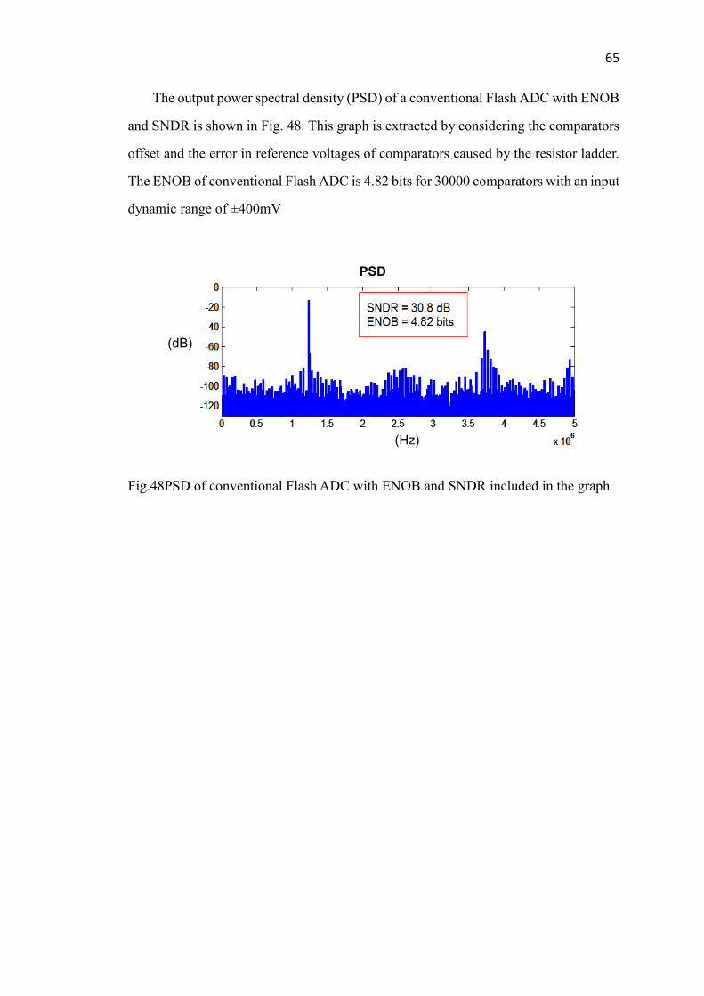
65
PSD
(dB)
(Hz)
The output power spectral density (PSD) of a conventional Flash ADC with ENOB
and SNDR is shown in Fig. 48. This graph is extracted by considering the comparators
offset and the error in reference voltages of comparators caused by the resistor ladder.
The ENOB of conventional Flash ADC is 4.82 bits for 30000 comparators with an input
dynamic range of ±400mV
Fig.48PSD of conventional Flash ADC with ENOB and SNDR included in the graph

66
Table V shows a comparison between the proposed stochastic ADC, conventional Flash
ADC, conventional stochastic ADC and multiple comparator group (MCG) stochastic
ADC. As predicted in the theoretical analysis, 80% of the used comparators are actively
taken part in the conversion process and the input dynamic range is increased from ±σ
in conventional and MCG stochastic ADCs to ±3σ in the proposed stochastic ADC.
TableV Comparison between the proposed stochastic ADC and the other different
architectures
This work
This work
Stochastic
ADC
MCG ADC Flash ADC
ENOB 7.23bit 6.6bit 4.2bit 6bit 4.5bit
Active
comparators
65% 80% 68% 48% 80%
Input range ±350mV-
±250mV
Variable
(±500mV
-±350mV)
±153mV ±153mV ±400mV
Comparator
trip points
Uniformly
distributed
Almost
Uniformly
distributed
Gaussian
distribution
Piecewise
uniformly
distribute
d
Not
uniformly
distribute
d
Reference
signal
U-quadratic
distribution
U-quadratic
distribution
Ground ±(1.078σ)
V
Linear
voltages
Power
consumption
Pc+ PR Pc+ PR Pc Pc Pc+ PR
The estimated power consumption for the used dynamic comparator (@1GHz
sampling frequency) is 354.98 µW. The power consumption of the block of dynamic
comparators Pc=354.98 µw * M
where M is the number of comparators used in the ADC.
Resistor ladder power consumption used with @1GHz dynamic comparator is
estimated as (PR) 14.4 µW.

67
CHAPTER 6 FUTURE WORK AND
CONCLUSION
Future work:
The results achieved in this thesis are promising compared to the other architectures but
still there are certain recommendations for future research investigations which are
mentioned below:
The proposed architectures power consumption is a little bit higher compared to
standard stochastic ADC. This is due to the use of the resistor ladder for
generating reference voltages (Since Resistor dissipates power, the resistor
ladder used in this architecture consumes more power). Future research can be
done on decreasing the power consumption.
In this work, the active comparators is increased from 48% to 80%, but still
20% of the comparators will be either switch on or switch off all the time.
Future research may be focused on how to increase the active comparators.
Although the proposed architecture transfer function is almost linear within the
input dynamic range, the future goal should be to reduce the nonlinearity
present in the transfer function of the proposed architecture.

68
Conclusion:
A new architecture of stochastic ADC with uniformly distributed comparator trip points
is presented. The proposed architecture has an ENOB of 6.5 bits with an input dynamic
range of ±400mV while using 30000 comparators. To verify this proposed architecture,
a stochastic ADC is designed, using 90nm CMOS technology and compared with the
theoretical analysis. The ENOB obtained almost matches with the theoretical results
with almost 80% comparators fall within the useful input dynamic range.
.

69
Appendix A
TableIV Code to generate reference values for system level results
Line No Matlab code
1
2
3
4
5
6
7
8
9
10
11
12
13
14
X=0.153.*randn(1,1024)
y1=-0.5+0.1*rand(1,127);
y2=-0.4+0.1*rand(1,115);
y3=-0.3+0.1*rand(1,100);
y4=-0.2+0.1*rand(1,90);
y5=-0.1+0.1*rand(1,80);
y6=0.1*rand(1,80);
y7=0.1+0.1*rand(1,90);
y8=0.2+0.1*rand(1,100);
y9=0.3+0.1*rand(1,115);
y10=0.4+0.1*rand(1,127);
y=cat(2, y1, y2, y3, y4, y5, y6, y7, y8, y9, y10);
y=randsample(y,1024);
trip_points=X+y;
Table IV shows the code used to generate reference voltages for system level
simulation. In line 1 a ‘randn’ function is used and this will generate 1024 random
samples, whose PDF will follow with ‘0’ mean and ‘0.153’ standard deviation. Line 2
to 13 is used to generate U-Quadratic distributed signal with desired ‘α’ and ‘β’
reference signals (reference signal). The function ’rand’ and how to use is described
below.
K= a+b.*rand(1, n);
APPENDIX

70
The above function will generate random uniformly distributed sample [24] with ‘a’
mean, ‘b’ standard deviation and ‘n’ number of samples with range specified by the
standard deviation.
The function ‘cat’ will concatenate all the uniformly distributed values from line 2 to
line 11 and function ‘randsample’ will pick 1024 values form the concatenated array.
This will be done by sampling at uniform intervals without any replacement. Line 14 is
used to generate comparator trip points after applying the reference signal (i.e., by
adding reference signal and comparators offset)
Appendix B
TableV OCEAN Script code for extracting the trip points of comparator after applying
reference voltages in TSMC 90nm technology
Line No Code
1
2
3
4
5
6
7
8
9
10
11
12
13
14
inp = infile( "input.txt" )
declare( a[1025] )
i=1
while( (i <= 1024)
gets(p inp)
a[i] = p
i = i + 1
p = outfile( "results.txt" "w" )
for( i 1 1024
analysis('tran ?stop "10u" )
desVar( "v" a[i] )
save( 'v "/net028" )
converge( 'ic "/net028" "0" )
temp( 27 )

71
15
16
17
monteCarlo( ?numIters "1" ?startIter i ?analysisVariation
'processAndMismatch ?sweptParam "None" ?sweptParamVals "27"
?saveData t ?nomRun "no" ?append nil ?saveProcessParams nil )
monteExpr( "mc" "average(clip(VT(\"/net028\") 9.5e-06 1e-05))" )
monteRun()
Table V shows the OCEAN script [25] file for extracting the comparators trip
points after applying reference voltages. Line 1 to 7 in the Table V is for reading the
reference voltages form a file. Line 8 is for creating an output file to store the
comparator trip points after applying reference voltage. Line 9 to 13 is to set number of
times Monte-Carlo analysis should run, applying one new reference voltage at every
new run and saving output voltage of the comparator at each and every run. Line 14 is
to mention that the comparator is working at 27 . Line 15 is to set the Monte-Carlo
analysis. Line 16 is to calculate the comparator trip point after applying reference
voltage.

72
Appendix C
Copyright form

73

74

75

76
BIBLIOGRAPHY
[1] David C.Brock., “Understanding Moore’s Law: Four Decades of Innovation”,
Chemical Heritage Foundation, 2006.
[2] Electronic-bus[online].
Available:http://electronicsbus.com/analog-vs-digital-electronics-design/
[3] David Nualart, “Stochastic Processes,” University of Barcelona [online].
http://www.mat.ub.edu/~nualart/StochProc.pdf.
[4] Jacob R.Baker., “circuit design, layout, and simulation”, Wiley-IEEE Press.,3rd
edition 2010.
[5] Walt Kester, “Understand SINAD, ENOB, SNR, THD, THD + N, and SFDR so
You Don't Get Lost in the Noise Floor” Analog.com [Online].
http://www.analog.com/static/imported-files/tutorials/MT-003.pdf
[6] Hwei Piao Hsu “Probability, random variables and random processes”,
McGraw Hill Professional,1997
[7] Lambert M.Surhone, Miriam T.Timpledon, Susan F.Marseken “U-quadratic
distribution” VDM publishing, 2010
[8] Jun He, Sanyi Zhan, Degang Chen and Randall L. Geiger, ‘Analyses of Static
and Dynamic Random OffsetVoltages in Dynamic Comparators’,IEEE
Transactions on Circuits and Systems IVolume 56, Issue 5, Page(s):911–919.
[9] Skyler Weaver, Benjamin Hershberg, Un-Ku Moon ‘Digitally synthesized
stochastic flash ADC using only standard digital cells’ VLSI Circuits(VLSIC)
symposium, Page(s):266 - 267 15-17 June 2011..
[10] Engelberg.S, ‘The central limit theorem and low-pass filters’, 11th IEEE
international conference on Electronics, circuits and systems, 2004.ICECS,
Page(s):65-68 13-15 December.2004.
[11] (Journal) S. Weaver, B. Hershberg., and Un-Ku. Moon. : ‘Stochastic Flash
Analog-to-Digital Converter’, IEEE Transactions on Circuit and Systems,
November 2011, pp. 2825–2833H.

77
[12] S.C. Wong, K.H. Pan, and J.A. Ma, “A CMOS mismatch model and scaling
effects,” IEEE Electron Device Letters, vol. 18, no. 6, pp. 261–263, Jun 1997.
[13] Koon Lun Jackie Wong, “Comparison of Digital Offset Compensation in
Comparators,”UNIVERSITY OF CALIFORNIA, 2002.
[14] Jeon Heungjun, ‘A CMOS low-power low-offset and high speed fully dynamic
latched comparator’, IEEE international, SOC conference,pp. 285-288, 27-29
September 2010.
[15] L. Sumanen, M. Waltari, V. Hakkarainen, K. Halonen, “CMOS Dynamic
Comparatorsfor Pipeline A/D Converters,” IEEE ISCAS, vol. 5, pp. 157 - 160,
May 2002.
[16] M Morris Mano, “Digital Design”, Prentice Hall, second edition 1991
[17] Victor P.Nelson, H.Troy Nagle, Bill D.Carroll, J.David Irwin,’Digital logic
circuit analysis and design’,Prentice Hall, 1995
[18] Aezinia Fatemeh, M. L, ‘A Novel Low Power NOR gate in SOI
CMOSTechnology’, IEEE Asia pacific conference on circuits and systems, pp.
1403-1405, 4-7 December 2006.
[19] Nakajima Tomoya, “A Scalable Wideband Low-Noise Amplifierconsisting of
CMOS Inverter Circuits forMulti-Standard RF Receivers,” International
conference on SCS, vol. 33, pp. 1-4,6-8 November 2009.
[20] Hao Gao, Peter Baltusand Qiao Meng, “Low voltage comparator for High
speed ADC,” International symposium on Signals systems and Electronics
(ISSSE), pp. 1-4, 17-20 September 2010.
[21] T. W. Matthews, P. L. Heedley, “A Simulation Method for Accurately
Determining DCand Dynamic Offset in Comparators,” IEEE MWSCAS, pp.
1815 - 1818, Aug. 2005.
[22] Cooper, A.R, “Parallel architecture modified Booth multiplier,” Electronic
Circuits and Systems, IEE Proceedings G, June 1988, pp.125-128.
[23] Sumeer Goel, Ashok Kumar, Senior Member, and Magdy A. Bayoumi,
“Design of Robust, Energy-Efficient Full Adders for Deep-Submicrometer
Design UsingHybrid-CMOS Logic Style,” IEEE Transactions on VLSI systems,
pp. 1309-1321, Dec. 2006.

78
[24] Amos Gilat ‘ MATLAB: an introduction with applications’,Hoboken, NJ :
Wiley, 3rd edition 2008
[25] Lumerink, ‘OCEAN Reference’,
[online].Available:http://www.lumerink.com/courses/ece5411/Handouts/ocean
ref.pdf
[26] Mithun Ceekala, Kamal El-Sankary, Ezz El-Masry, “Stochastic ADC with
U-quadratic distributed reference voltages to uniformly distribute comparators
trip point,” Analog integrated Circuits and signal processing, Volume 74, pp.
461-465,Feb. 2013.
[27] Hyunju Ham, Toshimasa Matsuoka, Jun Wang, and Kenji Taniguchi, “Design
of a High-Speed-Sampling Stochastic Flash Analog-to-Digital Converter Using
Device Mismatch” Electronics and Communications in Japan, Vol. 96, No. 1,
2013
[28] Rabeeh Majidi, Anthony Crasso and John A. McNeill, “Digital Background
Calibration of Redundant Split-Flash ADC in 45nm CMOS” symposium on
Circuits and Systems (ISCAS), pp. 1271-1274,May. 2012