status of the dielectric wall accelerator · 2010-12-06 · status of the dielectric wall...
TRANSCRIPT
STATUS OF THE DIELECTRIC WALL ACCELERATOR*,+
George J. Caporaso#, Y-J. Chen, S. Sampayan, G. Akana, R. Anaya, D. Blackfield, J. Carroll, E.
Cook, S. Falabella, G. Guethlein, J. Harris, S. Hawkins, B. Hickman, C. Holmes, A. Horner, S.
Nelson, A. Paul, D. Pearsona, B. Poole, R. Richardson, D. Sanders, K. Selenes
c, J. Sullivan, L.
Wang, J. Watson and J. Weirb
Lawrence Livermore National Laboratory, Livermore CA 94551 aTomotherapy, Inc., Madison WI 53717
bCompact Particle Acceleration Corporation, Madison WI 53717
cTPL Corporation, Albuquerque, NM 87109
Abstract The dielectric wall accelerator (DWA) system being
developed at the Lawrence Livermore National
Laboratory (LLNL) uses fast switched high voltage
transmission lines to generate pulsed electric fields on the
inside of a high gradient insulating (HGI) acceleration
tube. High electric field gradients are achieved by the use
of alternating insulators and conductors and short pulse
times. The system is capable of accelerating any charge
to mass ratio particle. Applications of high gradient
proton and electron versions of this accelerator will be
discussed.
The status of the developmental new technologies that
make the compact system possible will be reviewed.
These include, high gradient vacuum insulators, solid
dielectric materials, photoconductive switches and
compact proton sources.
INTRODUCTION
This paper focuses on one concept that represents an
extreme variant of a high gradient accelerator that has
been under development as a compact flash x-ray
radiography source [1]. The system is called the Dielectric
Wall Accelerator (DWA) and employs a variety of
advanced technologies to achieve high gradient. Progress
towards the development of this concept is proceeding on
several fronts. The key technologies for any DWA are
high gradient vacuum insulators [2], high bulk breakdown
strength dielectrics for pulse forming lines, and closing
switches compatible with operation at high gradient. For
protons, we describe a very compact source capable of
generating substantial currents. In addition, some new
accelerator architectures will be described.
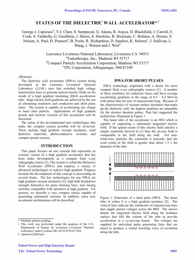
DWA FOR SHORT PULSES
DWA technology originated with a desire for more
compact flash x-ray radiography sources [1]. A number
of these machines are induction linacs and have average
accelerating gradients in the range of 0.3 – 0.5 MeV/m
with pulses that are tens of nanoseconds long. Because of
the characteristics of vacuum surface insulators that make
up the dielectric wall, the highest gradients are attainable
for the shortest duration pulses. That fact suggested the
architecture illustrated in Figure 1.
The beam tube of the accelerator is an HGI which is
capable of supporting a substantial tangential electric
field. If the spatial extent of this electric field satisfies a
simple constraint derived in [1] then the on-axis field is
comparable to the field along the wall. For non-
relativistic particles the constraint is basically that the
axial extent of the field is greater than about 1.5 x the
diameter of the tube.
Figure 1: Schematic of a short pulse DWA. The beam tube of radius b is a high gradient insulator [2]. The vertical lines indicate the conductors of transmission lines that supply pulsed voltages across the HGI. The arrows denote the tangential electric field along the insulator surface that fills the volume of the tube to provide acceleration to a co-moving bunch. The voltages are supplied by individual pulse generating lines that are timed to produce a virtual traveling wave of excitation along the tube.
* Multiple patents pending.
+ This work was performed under the auspices of the U.S.
Department of Energy by Lawrence Livermore National
Laboratory under Contract DE-AC52-07NA27344. # [email protected]
Proceedings of PAC09, Vancouver, BC, Canada TH3GAI02
Pulsed Power and High Intensity Beams
T16 - Pulsed Power Technology 3085

The pulsed voltages that are applied across the
dielectric wall in Figure 1 are generated by “Blumlein”
type structures with closing switches. The timing of the
switches determines the propagation speed of the virtual
traveling wave of excitation along the wall.
PHOTOCONDUCTIVE SWITCH
DEVELOPMENT
In order to generate pulses in the generic Blumlein
structures a good closing switch is required. The ideal
switch should have fast rise-time, low “on” resistance and
free from latch-up or avalanche at very high electric field
stresses. Wide bandgap materials illuminated with below
bandgap laser light offer this possibility. The below
bandgap light is able to propagate a cm or two through the
side of a wafer and illuminate the entire wafer volume,
permitting the placement of electrodes on opposite sides
of the wafer to take advantage of the high bulk breakdown
strength of these materials [3]. Both SiC and GaN wafers
have been used. SiC has been used with both 1064 and
532 nm radiation. It is important to note that these
devices are actually light controlled resistors.
Early tests used materials with “micropipe” defects in
the wafers which significantly compromised the bulk
breakdown strength of switches. Newly available
material is free from these defects.
Figure 2: Three failed SiC photoconductive switches that were soldered into Blumlein-like pulse generating lines. These switches are 1 cm x 1cm x 1mm thick with circular electrodes on top and bottom. The switches failed when charged to in excess of 30 kV for an average field stress of > 30 MV/m. Because of the geometry there is a x 10 field enhancement at the edges of the electrode that pushes the field to 350 MV/m, which is in excess of the bulk breakdown strength of the material. Each of the failures occurred at an electrode edge where the field stress was computed to be a maximum. Developing an enhancement-free, integrated switch package is the near term goal of our efforts.
The computed electric field stress for the configuration
used in the experiments is shown in Figure 3 along with a
schematic of the switch, electrodes, solder pads and oil.
The maximum field strength, well in excess of the
intrinsic bulk breakdown strength of SiC, corresponds to
the breakdown sites in the switches shown in Figure 2.
Figure 3: SiC photoconductive switch geometry and field stress distribution along the top surface of the wafer.
CAST DIELECTRIC MATERIAL
Ultimately we would like to use a cast solid dielectric
material in the pulse forming lines to simplify the fabrication process and to reduce the cost. For high gradient applications pulses on the order of a few nanoseconds are required. We have been working with
materials in which nano-particles of high dielectric
constant material are suspended in various base
substances such as epoxy, so as to permit adjustment of
the relative permeability of the composite. For low
concentrations of the nano-particles, the bulk breakdown
strength of the material under DC and pulsed conditions
in small samples is > 400 MV/m. In recent tests we have
measured the breakdown level for larger transmission line
structures that are relevant for the accelerator. A test
sample of the material is shown in Figure 4.
Figure 4: A test sample of the cast dielectric material in a transmission line configuration. These samples consisted of the base material only (epoxy) with no nano-particles. The dimensions of the sample are 4 cm x 22 cm. The separation between the two, parallel electrodes is 0.8 mm. The electrodes are 0.127 mm thick and 1 cm wide with rolled edges and are embedded within the epoxy. This sample failed along the edge of an electrode at a pulsed voltage of 140 kV for an average field stress between the electrodes of 170 MV/m.
TH3GAI02 Proceedings of PAC09, Vancouver, BC, Canada
3086
Pulsed Power and High Intensity Beams
T16 - Pulsed Power Technology

FIRST ARTICLE SYSTEM TEST (F.A.S.T.)
F.A.S.T. stands for First Article System Test, a small,
stacked Blumlein accelerator consisting of a small number
of solid dielectric pulse generators, photoconductive
switches and a high gradient insulator. The system is
designed as an integrated test of all of the relevant
components of an accelerator. F.A.S.T. is built with a
relatively small number of lines so that the system can be
easily disassembled to repair failed components at a
modest cost. All the switches are illuminated with an
expanded laser beam producing simultaneous firing of all
the pulse generating lines. While it was initially
anticipated that the FR-4 solid dielectric in the pulse
generating lines would be the electrical weak point, it
turned out that some switches failed via bulk breakdown.
Inspection revealed numerous structural defects (known
as “micropipes”) that are strongly suspected to have
compromised the bulk breakdown strength of the wafers.
Our first SiC wafers, from a different supplier, were free
of these defects and exhibited bulk breakdown strength
close to the expected value for pure SiC ( 250 MV/m).
We have since obtained new SiC from another source that
appears to be free of these structural defects.
The pulse generating lines were coupled directly into
the HGI. Initial beam tests employed F.A.S.T. as a diode
by using a flashboard cathode to provide a source of
electrons. A wire mesh was placed on the anode side of
the HGI. Tens of Amps were extracted. Since the
impedance of the Blumleins was about 40 Ohms, the
electron beam constituted a negligible load on the lines.
As a consequence, the output voltage across the HGI
would ring for several cycles. With each cycle electrons
would be extracted from the source when the voltage was
of the proper polarity.
Figure 5: F.A.S.T. set up to accelerate electrons from a flashboard cathode. A 2.5 cm high HGI with a 4 cm bore is the wall of a diode. Two stacks of 7 “Blumleins” are shown feeding the HGI on either side. In some experiments, the diode was operated with a single stack. A sensitive beam current monitor is mounted below the HGI.
PROTON INJECTOR AND SOURCE
In order to accelerate protons through F.A.S.T. they
must move fast enough to cross the HGI during the 3 ns
accelerating pulse. This requires the protons have at least
200 keV before they enter F.A.S.T. This energy is
provided by the injector shown in Figure 6. The output of
the induction cells is summed along an internal stalk and
appears across a gap approximately 3 cm wide. The cells
are driven by cable Blumleins. The injector has been
operated at up to almost 300 kV.
Figure 6: Proton injector built from 5, 20 ns induction cells arranged in an inductive adder configuration to provide a voltage across a 3 cm gap. The source of Figure 7 and a series of gridded, pulsed electrodes, is used to generate the proton beam. F.A.S.T. sits in the white oil tank just below the injector.
Figure 7: A spark discharge source provides the protons through a small aperture. Titanium electrodes are exposed to a hydrogen atmosphere to absorb the gas (two different sources are shown mounted on an alumina substrate). In operation, a pulsed high voltage is applied to cause a spark between adjacent electrodes that liberates hydrogen gas and forms a plasma. A series of powered grids is used to extract ions, suppress electrons and to gate the output pulse.
Proceedings of PAC09, Vancouver, BC, Canada TH3GAI02
Pulsed Power and High Intensity Beams
T16 - Pulsed Power Technology 3087

ARCHITECTURE ISSUES
Stacked Blumleins, even in a stripline configuration,
are relatively low impedance structures. However, the
currents flowing in these lines produce magnetic fields
that close in adjacent lines. These fields induce currents in
those lines that act to reduce the voltage output and distort
the waveshape. The use of radial lines will eliminate these
parasitic couplings but the impedance of these structures
is exceedingly low, requiring massive currents to produce
high gradient.
Figure 8: Stacked Blumleins are subject to a parasitic coupling that induces currents in adjacent lines. These currents reduce the overall output voltage and distort the waveshape.
INDUCTION CONCENTRATOR
A possible solution to the problem of parasitic coupling
and the relatively low impedance of the stacked Blumlein
structures is to use a structure constructed inside of
conventional induction cells.
Consider the structure shown in Figure 9. It is an
inductive voltage adder in which the voltages of
individual induction cells are made to appear across a
small gap.
Figure 9: A typical electron injector made from induction cells. The sum of the voltage appears across the gap in the interior adder stalk.
If we could move the injector at the same speed as a
particle crossing the gap, it would be continuously
accelerated. A possible method for achieving this would
be to replace the adder stalk with a tube whose
conductivity could be quickly adjusted. Figure 10 shows
a technique to do this by using photoconductive switches
placed along an insulating tube.
The simplified transmission line circuit for this
structure is shown in Figure 11.
Figure 10: Inductive voltage adder with a stalk lined with photoconductive switches.
Figure 11: Simplified equivalent circuit for the structure of Figure 10. The distributed voltage sources represent the induction cells, the inductors and capacitors represent the distributed parameters of the coaxial region between the stalk and induction cells. The variable resistors represent the photoconductive switches. By illuminating these in sequence we can create a moving virtual gap that can provide continuous acceleration across the entire tube.
The transmission line equations for the voltage V and
current i are
V
x= g x,t( ) L
i
tR x, t( )i,
i
x= C
V
t (1)
where g is the source voltage per unit length supplied by
the induction cells, L is the inductance per unit length of
coaxial region between the inner stalk and the inner
surface of the induction cells, R is the resistance per unit
length of the switches (which is controlled by varying the
illumination level) and C is the shunt capacitance per unit
length. In addition, the electric field along the stalk,
which is the accelerating field, is simply given by
Ea = R x,t( )i . (2)
To analyze this circuit it is convenient to define
dimensionless independent and dependent variables.
Rot
L,
x
w,
Roi
go,
V
gow (3)
which are respectively, dimensionless time, distance,
current and line voltage. Here, w is the axial extent of the
virtual gap, Ro is the minimum resistance per unit length
of the switches and go is the maximum voltage per unit
length supplied by the cells (source function). In addition,
the resistance of the photoconductive switches and the
source voltage per unit length are given by
R ,( ) = Ro f ,( ), g ,( ) = goˆ g ,( ) . (4)
We now wish to look for a traveling wave of excitation
along the line. That is, we put
f ,( ) = fLu
Row
(5)
where u is the speed of the virtual gap.
TH3GAI02 Proceedings of PAC09, Vancouver, BC, Canada
3088
Pulsed Power and High Intensity Beams
T16 - Pulsed Power Technology

Consider a system that is very long so that we may
neglect the boundary conditions of the system and seek a
traveling wave similarity formulation of the problem.
That is, we seek a solution in which all dependent
variables are functions of the dimensionless quantity
Lu
Row. (6)
With equations (3) through (6) the system of equations
(1) can be reduced to
1 LCu2( )wRoCu
f ( ) =1 (7)
with
Ea = go f ( ) ( ) (8)
where we have taken the source function to be one.
Examination of equation (7) reveals that there are two
distinct regimes: LCu2<1 (“subluminal”) and LCu
2>1
(“superluminal”). This terminology arises from the fact
that 1/LC is the square of the speed of an electromagnetic
wave along the coaxial system described by equations (1).
If we assume that Ea is a constant over the gap we may
use equation (7) to solve for the dimensionless current.
Using equation (8) then specifies the function f. Analyses
of these two cases reveals that the maximum gain in the
strongly subluminal regime is given by
Ea
go1+
1
wRoCu (9)
while the maximum gain in the strongly superluminal
regime is given by
Ea
go1+
Lu
Row. (10)
To increase the gain as a particle is accelerated,
transition to the superluminal regime is desirable. One
way to accomplish this is to load the coaxial system of
Figure 10 with toroidal magnetic cores placed beween the
stalk and induction cells to increase L. The circuit model
is identical with a larger L.
There is a topological dual to the circuit in Figure 11 in
which the resistance and inductance are interchanged. In
this case the inductance can be produced by a helix along
the dielectric beam tube. The switches can be folded
inside the induction cells where they are used to power
the cells by connecting a capacitor bank across the cell
gaps. This arrangement is shown in Figure 12.
Figure 12: Topological dual to the circuit of Figure 11 in which L and R are interchanged. L is now provided by a helical winding along the dielectric beam tube.
We must now consider the effective resistance of the
cores in the induction cells that appears in parallel with
the variable switch resistance and source function.
A similarity solution for this case is shown in Figure 13.
for the case in which f is exponentially growing
(corresponding to carrier recombination after laser light is
removed from the switches). Compare this against a
numerical solution of the full equations for a 2 meter
section (with boundary conditions) as shown in Figure 14.
Figure 13: Similarity solution of the circuit corresponding to Figure 12 with core resistance in parallel with the source and switch.
Figure 14: Full numerical solution for a finite line with a wave launched at eta = 2 for the same case as Figure 13.
CONCLUSION
We have described the DWA component development status, discussed the proton injector and source for proton therapy development and have described a new accelerator architecture, the induction concentrator.
REFERENCES
[1] G. Caporaso, et. a., “High Gradient Induction Accelerator”, Proc. 2007 U.S. Part. Acc. Conf., TUYC02.
[2] S. Sampayan, et. al., IEEE Trans. Diel. and Elec. Ins. 7 (3) pg. 334 (2000).
[3] J. Sullivan and J. Stanley, “6H-SiC Photoconductive Switches Triggered Below Bandgap Wavelengths”, in Proc. 27 Int. Power Modulator Symposium and 2006 High Voltage Workshop, Washington, D.C. 2006.
Proceedings of PAC09, Vancouver, BC, Canada TH3GAI02
Pulsed Power and High Intensity Beams
T16 - Pulsed Power Technology 3089