startup 3: binky one port, pin, ddr and led
TRANSCRIPT
1
Atmel Startup 3: Binky One – PORT, PIN, DDR and LED
M. A. Parker, Angstrom Logic, LLC, Copyright 2015‐07‐28
Blinky One, the blinking LED, shows how to use the C/C++ language in Atmel Studio (AS) to control the
Atmel MCU ports for input and output (i.e., IO) and reveals the ‘secret’ life of the Atmel PORT, PIN and
DDR registers. Blinky One uses the circuit platform constructed for the previous Startup 2 as well as the
cable adapter constructed for the first Startup [0]. In all cases, we provide abbreviated reviews of the
circuit platform and the adapter for convenience. The next Startup develops Blinky Two in order to
illustrate the use of sensors with the pull‐up resistors internal to the MCU as well as discuss and
demonstrate bit operations. As with all the Startups, this instructable focuses on ‘getting started’ with
an Atmel Microcontroller MCU [1]. Working with the individual MCU offers significantly lower cost for
each project with much better control over the size, function and power requirements compared with
the MCU‐on‐a‐board systems such as Arduino [2] and the Rhaspberry Pi [3]. The Startup #5 Instructable
will convert the Blinky circuit and software (actually more like firmware once installed) for use with the
Lifeline that, although easy, provides means to correct clock settings for an MCU. Startup #2 described
and set the fuses in the ATTiny2313A using the constructed platform. It should be pointed out that the
Lifeline does not correct non‐clock fuses ‐ a high voltage programmer (12V) would be required as
discussed in Startup #5.
A good first Startup project consists of programming the ATTiny to blink an LED in order to become
familiar with some ATTiny programming and operation. Blinky One uses the same circuit as constructed
on the experimenter’s board and so nothing needs to be changed in hardware. Blinky One uses the first
secret of Atmel Input/Out – the Data Direction Register DDR. And actually, LEDs make an inexpensive
debugging tool for more complicated programs. Startup 4 will make a second Blinky that demonstrates
the use of an input pin. Startup #5 will show the Lifeline program which is essentially the Blinky program
but running on steroids at a much faster rate. In all cases, we first write and load the program [4] into
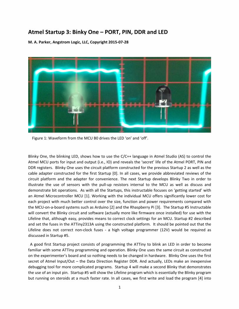
Figure 1: Waveform from the MCU B0 drives the LED ‘on’ and ‘off’.

2
the MCU, then view the effects on the LED, and then afterwards, explain the C++ statements used in the
programs. The references [5‐11] include some example language references for C/C++.
We begin the programming and coding. While this Instructable explains each coding statement, the
reader might still want to consult some of the many excellent C/C++ references [5‐11].
Step 1: The Circuit
By this point, two separate components should have been constructed: the programming cable adapter
and the circuit on an experimenter’s board (Figure 2). These should have been tested in Startup #2 [0]
by setting the fuses for the ATTiny2313A.
Make sure the breadboard circuits has been connected as shown in Figure 2. Be careful that the 9v
battery positive terminal connects to the regulator input and NOT the 5v rail at the top of the
breadboard. Keep in mind: do not reverse bias the MCU (or else kaput), do not reverse bias the
capacitor (or else stinky kaput), do not reverse bias the LED (or else maybe nothing). The capacitors and
resistors either have the value printed on the side or else they have codes as shown in References
[12,13].
For the LED, choose Red or Green for use with the 2.2k resistor shown in the schematic. Blue will be ok
but you might want to change the resistor to 1.5k to make it brighter. It is always good to have an ample
supply of LEDs and resistors.
Figure 2: Schematic diagram of the Blinky circuit replicated from Startup #2. See the parts
list for the components and brief not on constructing the adapter.

3
As a point worth remembering, do not connect any powered 5v device to an MCU running on less than
5v since generally an over voltage of 0.5V – 0.7V is enough to smoke the MCU.
Step 2: Create the Lifeline solution if not previously created
This Step should be skipped if the Lifeline solution was previously created in Startup 2. The abbreviated
procedure appears below.
1. Connect the programmer to the USB port and start Atmel Studio 6 (AS6). 2. Click the menu sequence Files > New Project. Choose C++Executable. 3. Next to ‘name’ type ‘Atmel Lifeline’. Check the box next to ‘Create Directory for Solution’. 4. The Device Selection Dialog pops up. Select ‘ATTiny 2313A’. Click OK. 5. Select the Atmel menu sequence: Project > Atmel Lifeline Properites.
Select the left hand Device tab and verify Device = ATTiny2313A Select the Tool tab and Select your programmer. The ISP Clock of 125 kHz will work – this value must
match the one set in Tools > Device Programming. It must be less that ¼ of the clock rate of the MCU to be programmed. 6. Connect the 9V battery to the experiment’s board circuit and connect the programmer to the board through the adapter cable previously constructed. 7. Select the Atmel menu sequence: Tools > Device Programming. Verify that the Tool box displays your programmer and the device box displays ATTiny2313A, and the acronym ISP should appear in the 3rd box. Read the Target Volts – it should be within a few percent of 5V. Set the ISP Clock to 125 kHz to match that in Item 5 above. 8. Save and close the solution. Note: The full solution can be saved by clicking the icon showing multiple disks in the tool bar or else use File > Save All.
Step 3: Open the existing Lifeline solution
As mentioned in previous Startups, the Atmel Studio AS essentially uses the Microsoft Integrated
Development Environment IDE for the Visual Studio VS. The files produced by AS (and VS) are bundled
together to form a Solution rather than a program. Open the existing Atmel Lifeline solution as follows.
We follow this procedure each time we open an existing solution (except we don’t mess with the fuses
once they have been set).
1. Connect the programmer to the USB port and attach it to the experimenter’s breadboard through the
cable adapter constructed in Startup #1. Connect the battery to the 9v batter clip.
2. Start Atmel Studio. Open Lifeline using the menu sequence:
File > Recent Projects and Solutions > Atmel Lifeline.atsln
3. Select the Atmel menu sequence: Project > Atmel Lifeline Properites. Select the left hand Device tab and verify Device = ATTiny2313A Select the Tool tab and verify your programmer. The ISP Clock of 125 kHz will work – this value must
match the one set in Tools > Device Programming. It must be less that ¼ of the clock rate of the MCU to be programmed. 4. Select the Atmel menu sequence: Tools > Device Programming. Verify the Tool box names your programmer and the device box names ATTiny2313A, and the 3rd box should show ‘ISP’. Click the APPLY

4
button. If AS wants to upgrade the programmer firmware then go ahead and do it. If an error occurs then refer back to Startup#1 [0]. Next, read the Target Volts – it should be within a few percent of 5V. Set the ISP Clock to 125 kHz to match that in Item 5 above. Do not close the dialog – proceed to Item 5 below. 5. If the fuses have not been set for the current ATTiny2313A, then verify the following settings by
clicking the fuses tab on the left. Refer to Startup #2 for details. Caution Caution Caution: Do not
unnecessarily play with the fuses! And definitely don’t look cross‐eyed at the ‘Lock Bits’ at this time –
they are used to prevent the viewing of flash content – different MCUs have different lock bits.
SELFPRGEN: No Check; DWEN: No Check; EESAVE: No Check; SPIEN: Checked; WDTON: No Check;
BODLEVEL: Disabled; RSTDSBL: No Check; CKDIV8: No Check; CKOUT: No Check;
SUT_CKSEL: INTRCOSC_8MHz_14CK_0MS
Step 4: Atmel Secret: DDRs and PORTs and PINs
This current Step takes a break from construction and test. People often ask (and should ask) how to
toggle the voltage level (i.e., logic state) on an MCU port pin to make an LED blink (Figure 1) and how to
read a digital input.
Often with respect to a microcontroller (MCU) or processor, one speaks of ‘port’ meaning a group of
wires that either brings data out of the MCU or into the MCU. For an integrated circuit, the ‘wires’ refer
to the physical pins on the IC. The Atmel AVR MCUs generally have ports with 8 pins each since the MCU
uses 1 byte wide data busses. The ports are often referred to as Input‐Output ports or as IO ports or as
just IO; these are the digital IO ports. The Atmel MCUs can have many such IO ports that are labelled as
A, B, and so on. One often finds the Atmel key words of PORTA, PORTB, PORTC, PORTD. Please reread
this paragraph and notice that a physical port refers to the physical pins on the IC. Atmel uses the
keywords of PORT and PIN (note caps) in reference to Output and Input and registers. By way of
definition, a register [14] is a type of memory location (perhaps better termed ‘storage location’) with
special relations/interconnectivity to hardware. The register is not considered to be part of program and
variable memory although it might be possible to read, write, manipulate and transfer the register
contents.
Now here’s part of the secret. In Atmel jargon, the word PORT (as used in PORTB for example) refers to
a digital OUTPUT port whereby the MCU will generate a voltage on the wires exiting the MCU. The
Atmel word PIN (as used in PINB for example) means the MCU places the group of physical wires in a
high impedance state and the MCU can read the digital voltages (0 or Vcc where Vcc = 5 for the
experimenter’s board setup). Perhaps more importantly, PORTB and PINB refer to the same group of
physical wires on the MCU. A similar comment applies to PORTA and PINA except the physical pins will
general differ from those to which PORTB and PINB refer. So how does one determine whether a
physical pin on the MCU is an input or an output for the MCU?
Let’s say this again with other words. There’s a difference between PORT and PIN in ATMEL using C/C++.
The word PORT refers to a register that provides outputs to the MCU physical pins. The PORT register
stores 1s and 0s and the MCU translates these logical values to voltages of Vcc and zero, respectively, at
5
the physical pins. The word PIN refers to a register that receives the input from a group of physical pins.
The MCU will translate the voltages of Vcc and zero on the physical pins to logical 1s and 0s,
respectively, for the PIN register. Notice the word physical refers to the actual short wires protruding
from the MCU package. We often use the word ‘port’ in reference to the collection of 8 pins; this should
be read as physical port and physical pins.
OK, so how does one specify whether a physical pin is an input or an output for the MCU? Atmel AVR
uses the concept of Data Direction Register DDR. Each group of wires forming a physical IO port has such
a DDR and labeled as DDRA, DDRB, DDRC, DDRD and so on. A DDR is an 8 bit register (i.e.,
memory/storage location) similar to the corresponding register for the 8 bit IO ports. A value of 1 in a
DDR position corresponds to an output for the corresponding physical pin. A value of 0 produces an
input on the corresponding physical pin. As an example, DDRB corresponds to physical PortB. When
DDRB bit #i has the value of 1 then pin #i in physical PortB will be an output for the MCU. On the other
hand, when DDRB bit #i has a zero value then physical pin #i in physical PortB will be an input. Perhaps
more concrete examples would be better.
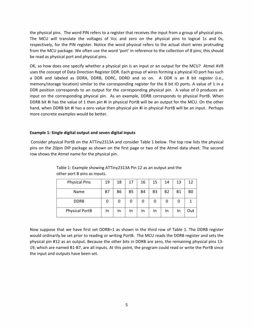
Example 1: Single digital output and seven digital inputs
Consider physical PortB on the ATTiny2313A and consider Table 1 below. The top row lists the physical
pins on the 20pin DIP package as shown on the first page or two of the Atmel data sheet. The second
row shows the Atmel name for the physical pin.
Physical Pins 19 18 17 16 15 14 13 12
Name B7 B6 B5 B4 B3 B2 B1 B0
DDRB 0 0 0 0 0 0 0 1
Physical PortB In In In In In In In Out
Now suppose that we have first set DDRB=1 as shown in the third row of Table 1. The DDRB register
would ordinarily be set prior to reading or writing PortB. The MCU reads the DDRB register and sets the
physical pin #12 as an output. Because the other bits in DDRB are zero, the remaining physical pins 13‐
19, which are named B1‐B7, are all inputs. At this point, the program could read or write the PortB since
the input and outputs have been set.
Table 1: Example showing ATTiny2313A Pin 12 as an output and the
other port B pins as inputs.

6
Example 2: Two output pins and 6 inputs
Physical Pins 19 18 17 16 15 14 13 12
Name B7 B6 B5 B4 B3 B2 B1 B0
DDRB=00000110 0 0 0 0 0 1 1 0
Physical PortB In In In In In Out Out In
The third row of Table 2 shows that we have first set DDRB = 00000110 in binary. In C/C++ this is written
as DDRB = 0b110 where the ‘0b’ means ‘binary’. The leading zeros have been omitted for simplicity to
form the ‘110’ part but they can be included in the C statement as DDRB = 0b00000110 if desired. The
same value can be written in decimal as DDRB=6. And it can be written in hexadecimal as DDRB = 0x06
where the ‘0x’ stands for hexadecimal. The physical PortB therefore has pin13 and pin 14 as outputs and
all other pins as inputs.
Comment: Those physical pins that are outputs will be able to generate either of two states, namely,
zero and Vcc. For our project, the experimenter’s board uses Vcc=5v while the Lifeline to be constructed
in a plastic box uses Vcc as the battery voltage, which can range from 4.9 volts to 3 volts depending on
the charge state of the batteries. The output voltage can then be used to control other components.
Atmel physical pins can either source or sink 40mA of current. To verify, refer to the Electrical
Characteristics in the spec/data sheets such as http://www.atmel.com/Images/doc8246.pdf. So the
output pin can provide (i.e., source) bias current when the physical pin has on output voltage of +Vcc or
it can receive current (i.e., sink) when the physical pin has 0v.
Table 2: Example with pin 13 and 14 as outputs and the rest inputs.

7
Example 3: Write values to outputs
Ok so let’s take a couple examples for using DDRB, PORTB and PINB. First consider the PORTB.
Physical Pins 19 18 17 16 15 14 13 12
Name B7 B6 B5 B4 B3 B2 B1 B0
DDRB 1 1 1 1 1 1 1 1
Physical PortB Out Out Out Out Out Out Out Out
PORTB=0b0100100 0 1 0 0 0 1 0 0
Physical Pin Result 0v Vcc 0v 0v 0v Vcc 0v 0v
In the example of Table 3, we first set DDRB = 0b11111111 = 0xFF =255 decimal so that physical pins 12‐
19 are all outputs for the MCU. Next suppose we write the following byte to the output register for B as
PORTB=0b0100100 as shown in the sixth row of Table 3. Note ‘PORTB=’ means to set the PortB output
register to a value – it’s easier to think of PORTB as a variable and ‘PORTB=’ means to set that variable
equal to a value, which the MCU translates to voltages on the physical port. When PORTB has logic ‘1’,
the output should exhibit the physical realization of the ‘1’ which is Vcc or, for our experimenter’s
board,
Logic 1 => Vcc=+5volts
Using logic 1 in this manner allows for a great many different platforms to use the same coding so long
as the MCU knows how to transform the logic values into voltages. So comparing the sixth and seventh
rows of Table 3 shows that those physical pins to which a logic 1 has been written will exhibit a voltage
of Vcc. The other pins have zero volt potential. IMPORTANT POINT: The characters “PORTB=” in this
case means to WRITE something to the physical pins in PortB (actually this first writes to the PORTB
register and then the logic values are translated by voltage generating circuitry in the MCU). In this
way, the MCU can control external circuitry.
Table 3: An example making IO Port B pins outputs.

8
Example 4: Read values from input pins
Now consider another case where we first set (in our program) DDRB = 0b00000000 (binary) = 0x00
(hex) = 0 (decimal) as in Table 4. Here all of the physical pins 12‐19 will be inputs because of all the zeros
in DDRB.
Physical Pins 19 18 17 16 15 14 13 12
Name B7 B6 B5 B4 B3 B2 B1 B0
DDRB 0 0 0 0 0 0 0 0
Physical PortB In In In In In In In In
Applied Volts to Pin 0v 0v 0v 0v 0v Vcc 0v Vcc
PINB Contents 0 0 0 0 0 1 0 1
Further suppose some external agent (such as me or you) applies voltages to the MCU physical pins 12‐
19 as shown in the sixth row of Table 4. IMPORTANT POINT: Using “=PINB” means to read the voltages
present on the physical pins corresponding to IO PortB and convert them to logic values. This would be
used in a C/C++ assignment statement such as ‘x = PINB’. The contents of the variable x (i.e., PINB) can
be seen in the last row of Table 4 to have the value
x = 0b00000101 (binary) = 0x05 (hex) = 5 (decimal)
The MCU converts Vcc on an input pin to the logic value of 1 and zero otherwise. In this manner, the
MCU can read the states of external circuitry.
Example 5: Mixed IO and Pull‐up Resistors
There remains another possible situation whereby an IO port has both Input and Output and the MCU
performs a write to the port. What happens? For a pin that is an input, the write (using PORTB etc) can
enable or disable an internal pull‐up resistor depending on whether the corresponding bit in the write is
a 1 or 0 respectively. Refer to Startup 4. Reading a port (using PINB etc) of mixed IO (some pins in the
port are output and the rest are input) will read the input when the pin is set as input and it will read the
previously written value (which is still in the PORTB register) if the physical pin is an output. Refer to
Startup 4 or to the user manual for details [0,1].
Now to code the Blinky One project.
Table 4: Example showing Pins 12‐19 are all inputs.

9
Step 5: Blinky One – Ready the Coding Page
Now it’s time to start coding but we first need to ready the coding page named ‘Atmel Lifeline.cpp’.
Once the Atmel Lifeline solution has been opened, the file name ‘Atmel Lifeline.cpp’ will appear on the
right hand side of the IDE in the ‘Solution Explorer’ panel and possibly as a tab under the AS tool bars.
1. Make sure the programmer is connected to the Experimenter’s board and also to the USB port.
Make sure the power is applied to the experimenter’s board.
2. Start AS6
3. Click File on the top menu strip, place the mouse pointer on Recent Files and select “Atmel
Lifeline” (or open it using Open). On the top AS6 menu strip, click ‘Project > Atmel Lifeline’ and
then click ‘Tool’ in the left menu and make sure the programmer is set to your programmer
(either AVRISP or Atmel ICE) and set ‘ISP Clock’ to 125kHz. Close this dialog.
Next, click on Tools > Device Programming found in the top AS6 menu strip. Make sure that your
programmer is selected (either AVRISP or Atmel ICE) and the correct device appears
(ATTiny2313A). Click Apply next to the ISP box. Click the Read Signature and Voltage buttons
and the voltage measured by the programmer should be within a few percent of 5V. Now set
the slider ‘ISP Clock’ for 125 kHz and then click the SET button. Close out of the Device
Programming dialog. The procedure of this item should be carried out each time a solution is
opened in AS. If the two ISP Clocks do not have the same value, then AS will not properly load
the software/firmware into the MCU.
4. Make sure that the Atmel Lifeline.CPP (for C++ language) or Atmel Lifeline.C (for C language)
coding forms can be seen. It will have /* at the top with the name of the program. The code
window can be viewed by either clicking the Atmel Lifeline.cpp tab just under the icons in the
top tool bar, or else double clicking the Atmel Lifeline.cpp file name appearing on the right hand
side under Solution Explorer.
5. Remove the line reading “// To Do:: Please write … code.” ‐ it is a comment line.
The lines between /* and */ at the top are comments and do not compile with the rest of the
program. Any single line with // is also a comment and does not compile. Any text starting with
// after the semicolon is a comment and does not compile.
6. Do not turn off the circuit and do not disconnect the programmer and do not close AS6.

10
Step 6: Blinky One – Enter the Blinky One Program
Modify the Atmel Lifeline program to look like the following although the colors might vary but the color
is not important at the moment – just type the text. The line ‘#include <avr/io.h> ‘ should already be
present as should a few others. Make sure to observe and keep the case of the text (i.e., retain the
capitalized and non‐capitalized text). Make sure to accurately place the semicolons at the end of the
lines. Make sure to keep all braces and parentheses.
#include <avr/io.h> #define F_CPU 8000000UL #include <util/delay.h> int main(void) { DDRB = 0b00000001; // or 0x01; should have 8 bits while(1) { _delay_ms(1000); PORTB = 0b1; _delay_ms(1000); PORTB = 0x00; } }
The meaning of the lines of code will be described later below. For now, we want to see the LED blink.
Step 7: Blinky One – Compile and run
Several methods can be used to compile and run Blinky or any other program. Use method ‘b’ but be
aware of method ‘a’.
1. Compile, Error Check, and Create File (F7)
The program can be checked for errors without loading the program into the MCU by clicking on
the Build menu item at the top of AS and then click the Build Solution item in the drop down list.
The result of the compile will appear in a window at the bottom of AS6. Notice the two tabs at
the very bottom: Error List and Output. If all is successful, the Output window will show ‘Build
succeeded’. If there is a typing error then the Error window will show the error and the line
number. The errors need to be corrected for the program to run. If your code compiled
successfully, consider adding an error to see what happens when the program compiles but
remember to correct the error! By the way, warnings should be corrected too. Building the
solution will also save the solution text to file as well as the Hexadecimal file. Some people
prefer to program the MCU with the Hex file rather than going through the trouble of compiling
the entire solution again.

2. Lo
C
th
p
co
A
w
Step 8:
Blinky sw
Figure 2)
in Figure
need to b
between
Pmax. Ob
will have
power Pm
Now, wha
applied to
output po
which is t
must be la
For an an
LED as giv
where k i
LED is ide
current I t
oad, Compile
lick on the sm
he two vertic
erform the s
ompiled prog
t this point, t
will see the Lif
Blinky One
witches the L
from +5V to 0
1. Take note
be able to se
Blinky and Li
bviously, whe
zero output
min will be Pm
at would hap
o the LED‐Res
ower would b
the approxim
arger than Vt
alysis, assum
ven by
s a positive c
entical to the
through the r
, Error Check,
mall triangle
cal bars). The
same operati
gram will be lo
the LED shoul
feline program
e – LED Br
LED‐Resistor
0V and back w
of the bright
ee the differe
feline. Call th
n Pin 12 has
power so th
min=0.
ppen if a volta
sistor combin
be Pmax/2. B
mate voltage d
th for the LED
e that the po
constant. To p
current thro
resistor R will
, and Create
on the Tool b
e same effect
ons as in ‘a’
oaded into th
ld be blinking
m produces b
ightness
combination
with a result
ness at each
ence in LED
he brightest e
zero voltage
e minimum o
age V=2.5 vo
ation? One m
But this is no
dropped acro
D to light [15‐1
ower P of the
P=
predict P, we
ugh the resis
be given by O
11
File (F5)
bar (Figure 3,
t can be had
’ above but
he MCU and it
g. Take note o
rightness som
(schematic o
similar to tha
level. We wi
optical powe
emitted powe
e then the LE
output optica
lts were to b
might think th
t the case be
oss the LED w
16].
emitted light
=kI
e need to kno
tor. If Vr is th
Ohm’s Law
, fifth icon fr
by pressing
in addition,
t will run. If t
of the LED bri
mewhere in b
of
at
ill
er
er
D
al
be
he
ecause an LE
when forward
t is proportio
ow the curren
he voltage dr
Figu
tria
pre
Figure 4
om the left –
F5 on the ke
if there aren
there are erro
ightness both
between ‘on’
D has a thre
d biased. The
nal to the cur
nt I. The cur
rop across the
ure 3: The sm
angle can be c
essing F5.
4: LED‐Resisto
– not the one
eyboard. AS
n’t any errors
ors, correct th
h ‘on’ and ‘off
and ‘off’.
shold voltage
e applied volt
rrent I throug
rrent I throug
e resistor the
mall, right‐poin
clicked instea
or Voltages
e with
S6 will
s, the
hem.
f’. We
e Vth,
tage V
gh the
(1)
gh the
en the
nting
d of

12
I = Vr/R (2a)
The voltage drop across the resistor (Figure 4) will be the difference between V and Vth, namely Vr=V‐
Vth, and so Ohm’s Law becomes
I=(V‐Vth)/R (2b)
As a result, the emitted power from the LED depends on the voltage V applied to the LED‐Resistor
combination
P = k I = k ( V – Vth ) / R for V > Vth (3a)
P = 0 for V < Vth (3b)
where Vth is the approximate voltage drop across the LED. The threshold voltage Vth can range from 1
volt for IR LEDs to more than 3.5 volts for deep UV LEDs. In other words, threshold voltage is roughly
inversely proportional to the emission wavelength Vth ~ 1/wavelength. Blue might have Vth = 3.3 and
red might have Vth=1.8. So according to Equations 3, the emitted power is not proportional to the
applied voltage. In fact, if Vthr = 2.6 and the voltage applied across the LED‐resistor combination is V=2.5
then approximately zero power will be emitted from the LED which is definitely not ½ Pmax.
Now on the other hand, what will be the brightness if we cycle the LED‐resistor combination very fast
(1.5MHz) between +5 volts and 0 volts? Our eyes cannot distinguish the discontinuity of light changes
faster than around 20‐30Hz. The Lifeline operates at a much higher frequency of 1.5MHz. In such a case,
we expect our eyes/brain to register approximately an average of the maximum emitted power Pmax
(when Vcc is applied across the LED‐Resistor combination) and the minimum emitted power Pmin=0
(when zero volts is applied to the combination). Assume that the time ‘on’ is the same as the time ‘off’
(i.e., Duty Cycle D = 1/2 or 50%) so that the average should be
Pave = (Pmax+Pmin)/2 = (Pmax+0)/2= Pmax/2 (4)
The analysis is only approximate for high modulation rates since the LED can have capacitances and
material properties that should be included, and our eyes might not respond as assumed. The switching
between rails (0V and Vcc) is similar to Pulse Width Modulation PWM with a duty cycle D=0.5 (i.e., 50%).
In fact, duty cycles D other than 50% can be included as
Pave = D * Pmax + (1‐D) Pmin or P = D * (Pmax‐Pmin) + Pmin (5)
The Lifeline uses the LED‐resistor combination as an indicator of the proper operation of the MCU. The
LED will not APPEAR to be ‘on’ all the way (i.e., Pave won’t have the value Pmax) and it won’t APPEAR to
be off all the way (i.e., we won’t have Pave=0) because our eyes/brain can only see something related to
the average for fast blinking.

13
Step 9: Blinky One – Meaning of the Coding Statements
The references provide some very good books and articles for learning C and C++ for the Atmel MCUs [5‐
8, 11]. The items below essentially follow the order found in the Binky One program.
1. #include: A compiler directive to include a header file into the code with specified functions and
methods. Most of the header files can be viewed by placing the mouse cursor over the name
and right clicking and selecting ‘go to implementation’.
2. avr/io.h: Consists of other header files (i.e., .h extensions) for the specific MCU [17]. The header
files include keywords such as DDRB, PORTB, PB0, TIMSK, and TCNT0. Apparently io.h cannot be
viewed with the ‘go to implementation’ described in Item 1 above.
3. util/delay.h: Methods to delay program execution. Includes one to delay milliseconds and
another for microseconds.
4. #define x y: A compiler directive to substitute the text y whenever the text x is encounter in the
program. Often the compiler definitions are used so that the program can be easily changed
without searching through the entire code for all the places to change a parameter when
needed.
5. #define F_CPU 8000000UL: The compiler will substitute 8000000UL for the text ‘F_CPU’
whenever encountered in the code. NOTE: the delay.h header file requires the F_CPU to be
defined prior to importing delay.h since the delay.h file uses the F_CPU. The 8000000UL refers
to the clock speed. In our case, we are using 8MHz selected by the fuses. However, F_CPU of
16000000 would be correct for a 16MHz crystal for example. The UL at the end refers to
‘unsigned long’ integer.
6. int main(void): main is a function that every C and C++ program must incorporate. The program
execution starts at the ‘main’ function. The key word ‘int’ indicates that ‘main’ can return an
integer (16bits). Functions have arguments in parenthesis (). In this case, ‘void’ indicates the
function does not use a parameter. If we had the keyword void preceding the function name as
for example in ‘void main(void)’ then the function would not return a value – it would be a
subroutine.
7. Braces { }: The range of code defining the function ‘main’ is enclosed in { }. In fact, most C and
C++ coding structures (for example, ‘ switch’ and ‘if’) use braces { } to indicate their scope. Make
sure to include them!
8. Semicolons: Coding statements are terminated by the ‘;’. The statement can run across several
text lines as needed.
9. _delay_ms(x) : A method (i.e., function) defined in delay.h that delays program execution by x
milliseconds. In our case, x=1000 and so the delay is 1000mS which is 1 second. Notice tha the
parentheses surround the parameter x.
10. DDRB = 0b00000001: Data Direction Register for Port B. B0 will be an output and the rest will be inputs. For the ATTiny 2313A, the B0 is Pin12.
11. PORTB = 0b1: Sets B0 to 1 which translates to Vcc at the physical pin (12) corresponding to B0. A simpler and preferred way to write this statement is PORTB = 1; or PORTB = 0x01;
12. PORTB = 0x00; Sets B0 to 0 which translates to 0v at the physical pin (12) corresponding to B0. This could also be written as PORTB = 0;

14
13. while(x): The MCU will execute the statements between the ensuing two corresponding braces
{ } so long as the statement x is true. The x might question whether two variables a and b are
equal such as a==b (note the double equals). In our case, we want the LED to continuously blink
so the statements between the braces must continuously execute. We could write ‘while(true
== true)’ where ‘==’ is the C/C++ operator checking logical equality (a single ‘=’ means to assign
something to a variable such as in z=3). The statement ‘while(true==true)’ would cause the
infinite loop that we want since ‘true’ is always true. In our case, 1 is taken to be a ‘true’. So
‘while(1)’ will cause the infinite loop because this is the short cut for writing ‘while(true)’ which
is a shortcut for writing ‘while(true=true)’.
Step 10: Optional: Experiment with the Clock Rate
If you feel adventuresome, reprogram the clock fuse to change the clock rate. But caution! some
settings can render the MCU inoperative until the Lifeline has been completed in Setup 5. The crystal
can be added and tested. Just remember to undo any changes made to the software and circuit once
finished and prior to continuing to the next startups. Keep in mind that the Blinky One program has
been coded to have the LED ‘on’ for 1 second, ‘off’ for one second and then repeat.
Complete Step 2 and repeat Step 3 except for Item 5. Do not close the Tools > Device Programming
diaglog.
1. Operate at 4MHz internal clock rate
In the Tools > Device Programming, select Fuses on the left menu. Find SUT_CKSEL and select
INTRCOSC_4MHz_14CK_4MS for example. Click the Program button. The LED should now be ‘on’ for 2
seconds and ‘off’ for 2 seconds. Why? Because the timing statement ‘_delay_ms(1000)’ relies on the
statement F_CPU to provide the correct clock rate. If you change the Blinky One statement to read
‘F_CPU=4000000UL’ then the LED will once again blink ‘on’ for 1 sec and ‘off’ for 1 second. Be sure to
return the F_CPU=8000000UL. Set the fuse SUT_CKSEL = INTRCOSC_8MHz_14CK (or similar) if you do
not intend to complete the next item.
2. Crystal 16MHz
Refer to the crystal setup described in Startup #2, Step 2. Briefly connect the crystal to MCU pins 4 and 5
of the MCU (there isn’t any polarity). Connect a 22pF capacitor from MCU pin 4 to ground, and another
22pF capacitor from MCU pin 5 to ground. In the dialog for Tools > Device Programing choose the Fuse
menu on the left side. Set SUT_CKSEL=EXTXOSC_*MHZ_XX_14CK_4MS. Click Program. The LED should
blink ‘on’ for 1/2 second and ‘off’ for 1/2 second. The correct rate for blinking can be fixed by changing
the Blinky One statement to F_CPU=16000000UL. Once finished investigating this option, return the
clock fuse as SUT_CKSEL = INTRCOSC_8MHz_14CK (or similar), and F_CPU=8000000UL, and remove the
crystal and two 22pF capacitors.

15
Step 11: Parts List
The parts should already have been accumulated in Startup 1 and 2. However, the list will be repeated
here in brief for convenience.
1. Adapter: The construction of the programmer adapter appears in Startup 1 (see Reference [0]). In
brief, the adapter is constructed using a piece of double row male header available from
Amazon.com for example. Clip off a piece of the header so as to have 2 rows, 3 columns. Solder 6‐
inch 24guage plastic‐coated solid wires to the short side of the pins. Apply quick dry epoxy to the
side of the header with the short pins being sure to cover part of the wires (no more than about 1/4
inch and being careful not to put any epoxy on the longer side of the pins. Label the wires according
to Figure 2 in this text.
2. Atmel Programmer: ATATMEL‐ICE‐BASIC at Mouser.com or Digikey.com for about $55.
3. Atmel Studio AS6 (free): http://www.atmel.com/tools/atmelstudio.aspx
4. ATTiny 2313A: Digikey.com ATTINY2313A‐PU‐ND at $1.70 (pDIP package, 20pins).
5. Startup #5: 20 pin socket for DIP package (0.3” row spacing, 0.1” pin spacing), low profile:
Digikey.com ED3054‐5‐ND or AE9998‐ND for about 30cents. Similar sockets can be found on
Amazon.com.
6. LM7805 Regulator: Digikey.com LM7805CT‐ND or LM7806ACT‐ND for about 70Cents.
7. Electrolytic Capacitor 10uF, 50V: A large variety of capacitors but aluminum type will work ok:
Digikey.com: P997‐ND (mfr. number: Panasonic ECE‐A1HKS100) about 30cents. Actually Amazon
has a capacitor kit with both ceramic and electrolytic for $20 called “Joe Knows Electronics 33 Value
645 Piece Capacitor Kit” which looks like a reasonable set.
8. Ceramic Capacitor 0.1uF 50V: Again, a large variety available here. Digikey.com 399‐4454‐1‐ND
(Kemet C410C104M5U5TA7200) for about 25cents. See also the kit listed in #7 above.
9. Optional: Two Ceramic Capacitors 22pF (25‐100V ok) such as Digikey.com 490‐8663‐ND at 34 cents.
10. Optional: Purchase a crystal from the HC‐49US series or a series with a similar profile. Capacitance
loads in the range 18‐22pF more or less and less than about 50 Ohm equivalent series resistance ESR
will work ok. Amazon has nice packages of crystals as found by searching Amazon for 16MHz Crystal
or 8MHz Crystal etc. Here are some from Digikey.com:
16MHz Crystal from Digikey 300‐6034‐ND at 54cents each.
20MHz Crystal from Digikey 300‐6042‐ND at 54cents each.
8MHz:
8MHz Crystal from Digikey X164‐ND or X1093‐ND at 81cents each (but ESR=80).
8MHz Crystal from Digikey X100‐ND 70cents each (but larger profile)
Amazon.com: Search 8MHz Crystal – good selection, low profile, good ESR
10MHz Crystal from Digikey 887‐1010‐ND at 33 cents each.
11. LED: Amazon has a package of 50 LEDs of various colors for $10 (see Microtivity IL 185). Ebay has
many.
12. Resistor: Search Amazon.com for ‘resistor kit’. The SparkFun 500 1/4W resistor kit and the E‐
Projects – 400 Piece, 16 Value resistor kit look OK. Here are the values listed for Digikey:
1K Digikey.com: CF14JT1K00CT‐ND 10cents each
1.5k Digikey.com: CF14JT1K50CT‐ND 10cents each
2.2k Digikey.com: CF14JT2K20CT‐ND 10cents each
2.7k Digikey.com: CF14JT2K70CT‐ND 10cents each

16
3.3k Digikey.com: CF14JT3K30CT‐ND 10cents each
4.7k Digikey.com: CF14JT4K70CT‐ND 10cents each
5.6k Digikey.com: CF14JT5K60CT‐ND 10cents each
13. Resistor 10k required for the RST and 1k for using Lifeline with 3.3V. 1k Digikey.com: CF14JT1K00CT‐ND 10cents each
10k Digikey.com: CF14JT10K0CT‐ND 10cents each
14. Optional for Startup #4: Photo‐transistor. Order from either Digikey.com or Amazon.com
Digikey: Everlight PT334‐6C 38cents each
Amazon: Search ‘Everlight PT334‐6C’ about $5 for ten.
15. Optional for Startup #4: Photo‐resistor from Amazon. Just about any will work ok.
Amazon.com search for ‘photoresistor GM5539’. Cost $5 for ten.
Digikey PDV‐P8001‐ND by Advanced Photonics mfg # PDV‐P8001 for $2.22
16. 9v Battery clip: Radio Shack or search amazon.com for ‘9v battery clip’ (10 for $2).
Digikey.com: BS6I‐ND 60 cents.
17. The plastic housing for the Lifeline is constructed from a battery holder for 4 AA batteries that also
has a switch. These come from Radio Shack or Amazon.com. For amazon, search for ‘plastic battery
holder 4 AA switch’. Make sure the case holds 4 AA batteries and has a switch. I found a deal of five
cases for $8.
18. Experimenter’s breadboard: There are many types and sizes and places to purchase.
Amazon.com: MB‐102 Point Prototype PCB breadboard for $5 includes wires
Amazon.com: MB‐102 830 Solderless Breadboard for $4 with wires. 8‐32 screw 1.5” long.
19. Screw 8‐32 1.5inches long: check HomeDepot.com or Lowes.com. Any 8‐32” screw longer than 2”
will be ok so long as it is later cut to a length of 1.5”. You need two 8‐32 nuts. Many times the 8‐32
screws come with either a large flat head (truss head) or the smaller round heads (round head). Find
the round head since these fit better with the spring. The truss head would likely need to be filed
down.
20. 24 gauge solid core copper wire. 0ld telephone/intercom wire and intercom wire will work and has
many colors. The 24ga has a diameter of approximately 0.51 mm but it’s not critical.
Amazon.com: search on ‘4 conductor 24 awg cable solid copper’ either 60cents/foot or $20 for 100
feet. Ebay.com has nice 24 ga. solid core wire with multicolors. Search: ‘solid 24 gauge wire kit’.
Home Depot: 100 ft. 6‐conductor Indoor Phone wire for $20. I have not checked this for solid core
copper. For soldering the ICs and components, you might want to use 24ga stranded copper wire
since it is more flexible and less likely to pull loose from the joint. Amazon.com: search for ‘24 gauge
stranded wire’. Nice 6 spool kits (150’ total) will come up for $20.

17
Step 12: References
[0] The Atmel Startup articles, Instructables.com, 2015, M. A. Parker, Angstrom Logic: A. Atmel Startup 1: Atmel Studio and Programmer B. Atmel Startup 2: Microcontroller Circuits and Fuses C. Atmel Startup 3: Blinky One – PORT, PIN, DDR and LED D. Atmel Startup 4: Blinky Two – Switches, Pull‐Up Resistor, and Bit Ops E. Atmel Startup 5: Lifeline
[1] The complete Atmel manual for the ATTiny 2313A: http://www.atmel.com/Images/doc8246.pdf. More information on the ATTiny2313A can be found at http://www.atmel.com/devices/ATTiny2313A.aspx.
[2] Arduino products and learning: http://www.arduino.cc/
[3] Raspberry Pi products and learning: https://www.raspberrypi.org/
[4] Coding vs. Programming http://workfunc.com/differences‐between‐programmers‐and‐coders/
[5] The classic masterpiece: B.W. Kernighan, D. M. Ritchie, “The C Programming Language”, Prentice, 2nd
Ed. (1988). Available on amazon.com for $7.
[6] Good C++ review after reading the Kerninghan‐Ritchie book and some background in OOP. “C++
Super Review” written by The Staff of Research and Education Association, published by Research and
Education Associated (2000). ISBN: 0878911812. Amazon.com for $8.
[7] A good C++ tutorial site can be found at http://www.cprogramming.com/tutorial.html#c++tutorial
[8] Good overview of Atmel concepts and C but uses the AVR Butterfly: J. Pardue, “C Programming for Microcontrollers Featuring ATMEL’s AVR Butterfly and the free WinAVR Compiler”, Published by Smiley Micros (2005). ISBN: 0976682206. Amazon.com
[9] Keep in mind that avrfreaks.net has tutorials and project help http://www.avrfreaks.net/forum/newbie‐start‐here?name=PNphpBB2&file=viewtopic&t=70673 http://www.avrfreaks.net/forums/tutorials?name=PNphpBB2&file=viewforum&f=11
[10] SparkFun website has a variety of tutorials ranging from electronics to software: https://learn.sparkfun.com/tutorials/tags/concepts.
And a blinky here: https://www.newbiehack.com/MicrocontrollerTutorial.aspx.
[11] GCC reference:
http://www.gnu.org/software/gnu‐c‐manual/gnu‐c‐manual.pdf https://gcc.gnu.org/onlinedocs/ https://gcc.gnu.org/onlinedocs/libstdc++/
[12] Capacitor codes: http://www.wikihow.com/Read‐a‐Capacitor
[13] Resistor color code https://en.wikipedia.org/?title=Electronic_color_code

18
[14] Register definition:
https://en.wikipedia.org/wiki/Processor_register http://whatis.techtarget.com/definition/register http://homepage.cs.uri.edu/faculty/wolfe/book/Readings/Reading04.htm
[15] LED information: http://en.wikipedia.org/wiki/LED_circuit [16] LED information: http://www.gizmology.net/LEDs.htm [17] Content of avr/io.h: http://www.nongnu.org/avr‐libc/user‐manual/io_8h_source.html