standard for jsc lead-free control plans...
TRANSCRIPT

JSC-66491 Revision: Baseline July 2013
Standard for JSC Lead-Free Control Plans (LFCP) Engineering Directorate Avionic Systems Division
Verify this is the correct version before use Compliance is Mandatory
July 2013 Baseline
National Aeronautics and Space Administration Lyndon B. Johnson Space Center Houston, Texas 77058-3696
Downloaded from http://www.everyspec.com

Downloaded from http://www.everyspec.com

JSC-66491 Revision: Baseline July 2013
Change Record
Rev. Date Originator Approvals Description
Baseline July 2013 Baseline
Verify correct version before use at http://server-
mpo.arc.nasa.gov/Services/CDMSDocs/Centers/JSC/Home.tml. 3
Downloaded from http://www.everyspec.com

JSC-66491 Revision: Baseline July 2013
TABLE OF CONTENTS
1 GENERAL REQUIREMENTS ............................................................................................................. 5 1.1 SCOPE ................................................................................................................................................. 5 1.1.1 AUTHORITY ................................................................................................................................... 5 1.2 PURPOSE ............................................................................................................................................ 5 1.3 APPLICABILITY ................................................................................................................................... 5 1.4 ORDER OF PRECEDENCE ................................................................................................................ 5 1.5 APPROVAL OF DEPARTURES FROM THIS DOCUMENT ............................................................. 5 1.6 ROLES AND RESPONSIBILITIES ...................................................................................................... 6 2 APPLICABLE DOCUMENTS ............................................................................................................. 8 2.1 JSC DOCUMENTS .............................................................................................................................. 8 2.2 NASA STANDARDS AND DIRECTIVES ............................................................................................ 8 2.3 MILITARY STANDARDS ..................................................................................................................... 8 2.4 INDUSTRIAL STANDARDS ................................................................................................................ 8 2.5 REFERENCE DOCUMENTS .............................................................................................................. 9 3 LEAD-FREE CONTROL PLAN (LFCP) ........................................................................................... 10 3.1 PROJECT LEAD FREE CONTROL PLAN (LFCP) REQUIREMENTS ........................................... 10 3.1.1 LEAD-FREE CONTROL LEVEL DESIGNATION........................................................................ 11 3.1.2 LEAD-FREE TIN IDENTIFICATION AND REPORTING ............................................................ 11 3.1.3 TIN WHISKER RISK DOCUMENTATION ................................................................................... 11 3.1.4 TIN WHISKER MITIGATION ........................................................................................................ 11 3.1.4.1 DESIGN ................................................................................................................................. 11 3.1.4.2 HOT SOLDER DIP (HSD) .................................................................................................... 11 3.1.4.2.1. PRETINNING (PARTIAL HSD MITIGATION) ..................................................................... 12 3.1.4.3 CONFORMAL COATING ..................................................................................................... 12 3.1.4.4 EMBEDMENT / ENCAPSULATION ..................................................................................... 13 3.1.5 SURVEILLANCE (INSPECTION & FUNCTIONAL TEST) .................................................. 15 3.1.6 TIN PEST (TIN DISEASE) MITIGATION ............................................................................. 15 4 ACRONYMS AND ABBREVIATIONS AND GLOSSARY OF TERMS .......................................... 16 4.1 ACRONYMS AND ABBREVIATIONS ............................................................................................... 16 4.2 GLOSSARY OF TERMS.................................................................................................................... 16
Verify correct version before use at http://server-
mpo.arc.nasa.gov/Services/CDMSDocs/Centers/JSC/Home.tml. 4
Downloaded from http://www.everyspec.com

JSC-66491 Revision: Baseline July 2013
1. GENERAL REQUIREMENTS 1.1 SCOPE This document prescribes requirements for the control and mitigation of performance and reliability risks associated with the use of Lead-free Tin (Sn) and Lead-free Tin (Sn) technology in flight hardware, mission essential support equipment, and elements thereof.
1.1.1 AUTHORITY The authority for this document derives from requirement 5.f.5 of NASA Policy Directive 8730.2C (NPD-8730.2c) “NASA Parts Policy”.
1.2 PURPOSE This standard imposes a Lead-Free Control Plan (LFCP) to reduce the harmful effects of tin whiskers or tin pest in JSC-certified spaceflight hardware.
1.3 APPLICABILITY This document is applicable to JSC projects and programs, including JSC onsite and offsite contractors, developing and producing flight hardware, mission essential support equipment, and elements thereof. 1.3.1 Commercial Off-The-Shelf (COTS). The requirements of this document shall not apply to suppliers of commercial off-the-shelf (COTS) items. Projects which use COTS hardware for applications described above shall be responsible for identifying and managing risks associated with hardware that was built without a control plan to reduce the harmful effects of tin whiskers. The International Space Station (ISS) program document, SSP 50835, provides guidance on how a Program may address the impact of utilizing COTS hardware that was built without a control plan. 1.3.2 Existing or Previously Approved Designs. The requirements of this document shall not constitute the sole cause for the redesign of previously approved designs. When drawings for existing or previously approved designs undergo revision, they should be reviewed and changes made that allow for compliance with the requirements of this document.
1.4 ORDER OF PRECEDENCE The following shall be applicable in the resolution of conflict between the requirements or the text of this document; and, applicable documents, and approved / unapproved engineering documentation in the order indicated: a. Program Requirements b. This Document c. Engineering Documentation (i.e. : Approved Drawing)
1.5 APPROVAL OF DEPARTURES FROM THIS DOCUMENT Any changes, revisions, or deviations to the requirements of this document shall require technical evaluation and approval by the JSC Lead Free Control Board (LFCB) with the programs having waiver authority.
Verify correct version before use at http://server-
mpo.arc.nasa.gov/Services/CDMSDocs/Centers/JSC/Home.tml. 5
Downloaded from http://www.everyspec.com
JSC-66491 Revision: Baseline July 2013
a. Use of alternate control plans, documents, or processes shall require review and approval of the JSC Lead Free Control Board (LFCB)
b. Less stringent control plans, documents, or processes meeting Level "2B" are allowed in exceptional cases with the review and recommendation of the EEE Parts Control Board (EEE-PCB) and approval of the Lead Free Control Board (LFCB).
c. Requests for relief from requirements in this document shall be documented and adjudicated in accordance with NASA-STD-8709.20, Management of Safety and Mission Assurance Technical Authority (SMATA) Requirements as implemented by the programs.
1.6 ROLES AND RESPONSIBILITIES a. Project Function. Project shall generate a Lead-Free Control Plan (LFCP) in compliance with the
requirements of this document. Reference Appendix A, Project LFCP Template, as the minimum content required for a Lead-Free Control Plan (LFCP).
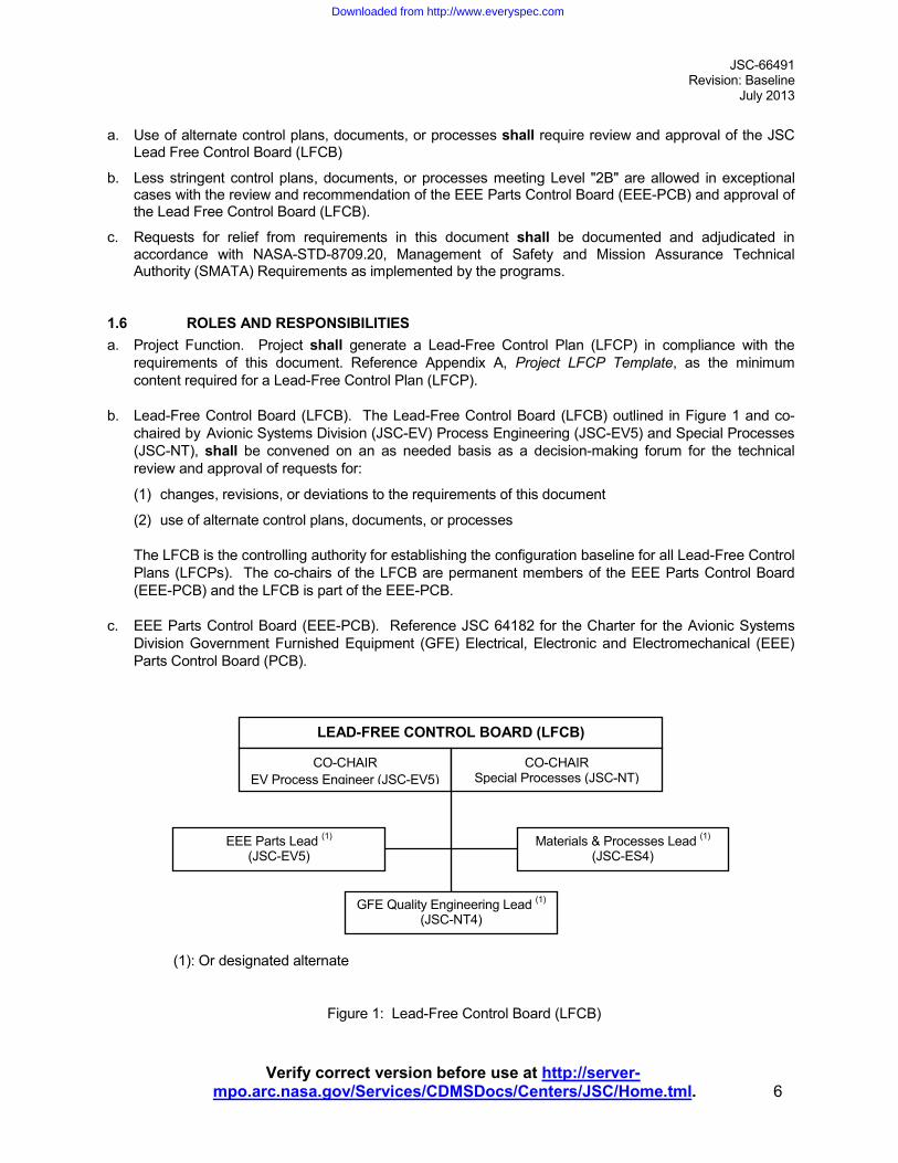
b. Lead-Free Control Board (LFCB). The Lead-Free Control Board (LFCB) outlined in Figure 1 and co-
chaired by Avionic Systems Division (JSC-EV) Process Engineering (JSC-EV5) and Special Processes (JSC-NT), shall be convened on an as needed basis as a decision-making forum for the technical review and approval of requests for:
(1) changes, revisions, or deviations to the requirements of this document
(2) use of alternate control plans, documents, or processes The LFCB is the controlling authority for establishing the configuration baseline for all Lead-Free Control Plans (LFCPs). The co-chairs of the LFCB are permanent members of the EEE Parts Control Board (EEE-PCB) and the LFCB is part of the EEE-PCB.
c. EEE Parts Control Board (EEE-PCB). Reference JSC 64182 for the Charter for the Avionic Systems Division Government Furnished Equipment (GFE) Electrical, Electronic and Electromechanical (EEE) Parts Control Board (PCB).
(1): Or designated alternate
Figure 1: Lead-Free Control Board (LFCB)
LEAD-FREE CONTROL BOARD (LFCB)
CO-CHAIR EV Process Engineer (JSC-EV5)
CO-CHAIR Special Processes (JSC-NT)
EEE Parts Lead (1) (JSC-EV5)
Materials & Processes Lead (1) (JSC-ES4)
GFE Quality Engineering Lead (1) (JSC-NT4)
Verify correct version before use at http://server-
mpo.arc.nasa.gov/Services/CDMSDocs/Centers/JSC/Home.tml. 6
Downloaded from http://www.everyspec.com
JSC-66491 Revision: Baseline July 2013
d. JSC Avionic Systems Division, Electronic Design and Manufacturing Branch (JSC-EV5). JSC Avionic systems Division, Electronic Design and Manufacturing Branch (JSC-EV5) shall approve all project LFCPs.
e. JSC Special Processes (JSC-NT). JSC S&MA Special Processes (JSC-NT) shall review all project LFCPs.
Verify correct version before use at http://server-
mpo.arc.nasa.gov/Services/CDMSDocs/Centers/JSC/Home.tml. 7
Downloaded from http://www.everyspec.com

JSC-66491 Revision: Baseline July 2013
2. APPLICABLE DOCUMENTS The following documents are applicable to the extent specified herein. The applicable revision shall be that identified herein or the revision in effect on the date of the contract or work authorizing document.
2.1 JSC DOCUMENTS
JSC 64182 ................................ Charter for the Avionic Systems Division Government Furnished Equipment (GFE) Electrical, Electronic and Electromechanical (EEE) Parts Control Board (PCB)
2.2 NASA STANDARDS AND DIRECTIVES
NASA-STD-8709.20 ................. Management of Safety and Mission Assurance Technical Authority (SMATA) Requirements
NASA-STD 8739.1A ................. Workmanship Standard for Polymeric Application on Electronic Assemblies
NASA-STD-8739.2 .................. Workmanship Standard for Surface Mount Technology (cancelled)
NASA-STD-8739.3 ................... Soldered Electrical Connections (cancelled) NPD 8730.2C ........................... NASA Parts Policy
NPD 8730.5B ........................... NASA Quality Assurance Program Policy NPR 7120.5 .............................. NASA Space Flight Program and Project Management Requirements
NPR 8705.4 .............................. Risk Classification for NASA Payloads
2.3 MILITARY STANDARDS
<None>
2.4 INDUSTRIAL STANDARDS
GEIA-STD-0005-1 ..................... Performance Standard for Aerospace and High Performance Electronic Systems Containing Lead-free Solder
GEIA-STD-0005-2 ..................... Standard for Mitigating the Effects of Tin Whiskers in Aerospace and High Performance Electronic Systems, Control Level 2C
GEIA-STD-0006 ...................... Requirements for Using Solder Dip to Replace the Finish on Electronic Piece Parts
IPC-1601 .................................. Printed Board Handling and Storage Guidelines
IPC J-STD-001E-2010 ............ Requirements for Soldered Electrical and Electronic Assemblies
IPC J-STD-001ES ................... Space Applications Electronic Hardware Addendum to IPC J-STD-001E Requirements for Soldered Electrical and Electronic Assemblies
IPC/JEDEC J-STD-020D.1 ..... Moisture/Reflow Sensitivity Classification for Non-hermetic Solid State Surface Mount Devices
IPC/JEDEC J-STD-033C ........ Handling, Packing, Shipping and Use of Moisture/Reflow Sensitive Surface Mount Devices
Verify correct version before use at http://server-
mpo.arc.nasa.gov/Services/CDMSDocs/Centers/JSC/Home.tml. 8
Downloaded from http://www.everyspec.com

JSC-66491 Revision: Baseline July 2013
2.5 REFERENCE DOCUMENTS The documents listed below provide technical guidance which may be helpful to readers of this document. Unless otherwise specified, the requirements and recommendations in these documents are not binding and are not to be construed as implied requirements to be imposed on the program.
GEIA-HB-0005-1 ....................... Program Management / Systems Engineering Guidelines for Managing the Transition to Lead-Free Electronics
GEIA-HB-0005-2 ....................... Technical Guidelines for Aerospace and High Performance Electronic Systems Containing Lead-free Solder and Finishes
GEIA-HB-0005-3 ..................... Rework/Repair Handbook to Address the Implications of Lead-Free Electronics and Mixed Assemblies in Aerospace and High Performance Electronic Systems
GEIA-STD-0003 ...................... Long Term Storage of Electronic Devices
IPC/JEDEC J-STD-609 ........... Marking and Labeling of Components, PCBs and PCBAs to Identify Lead (Pb), Pb-Free and Other Attributes
IPC-QL-653A ........................... Certification of Facilities that Inspect / Test Printed Boards, Components, and Materials
JSC-STD-8080.5 ..................... JSC Design and Procedural Standards
JSC 27301F ............................. Materials and Processes Selection, Control, and Implementation Plan for JSC Flight Hardware
MIL-D-3464E ........................... Desiccants, Activated, Bagged, Packaging, Use and Static Dehumidification (Type II)
MIL-HDBK-338B ...................... Electronic Reliability Design Handbook
MIL-STD-2073-1E ................... Standard Practice for Military Packaging (Method 50)
MS20003C ............................... Indicator, Humidity, Card, Three Spot, Impregnated Areas (Cobaltous Chloride), 30-40-50% RH
Metallurgical Assessment of Spacecraft Parts, Materials and Processes, Barrie D. Dunn, Wiley-Praxis, 1997, ISBN 0-471-96428-X
Verify correct version before use at http://server-
mpo.arc.nasa.gov/Services/CDMSDocs/Centers/JSC/Home.tml. 9
Downloaded from http://www.everyspec.com

JSC-66491 Revision: Baseline July 2013
3. LEAD-FREE CONTROL PLAN (LFCP)
3.1 Lead-Free Tin (Sn) For the purpose of this document, lead-free Tin (Sn) is defined as metallic Tin (Sn) containing less than 3 percent lead (<3% Pb) by weight as an alloying constituent. Lead-free Tin (Sn) technology is defined as electrical / electronic components and associated mechanical hardware and materials composed of, or coated / plated (internal / external surfaces) with metallic Tin (Sn) containing less than 3 percent lead (<3% Pb) by weight as an alloying constituent. Lead-free Tin (Sn) technology shall include:
• Lead-free Tin (Sn) coatings/platings, metallization, etc., on external surfaces of EEE components, mechanical parts, etc.; or, on internal cavity surfaces of EEE components (i.e.: hybrid, relay crystal cans, MEMS etc.).
• Lead-free Tin (Sn) solder alloys containing less than 3 percent lead (<3% Pb) by weight as an alloying constituent. Exception: Sn96.3Ag3.7
• Wiring technology (i.e.: wire, cable, connectors, terminators, clamps, braid / over-braid shield, etc.) composed of, or coated / plated with metallic Tin (Sn) containing less than 3 percent lead (<3% Pb) by weight as an alloying constituent.
• Any EEE components, electrical / electronic assembly, printed wiring assembly (PWAs), cable assembly, and/or wire harness assembly assembled with lead-free tin solder alloy except high temperature solder alloy Sn96.3Ag3.7 (Sn96A).
Note: Sn96.3Ag3.7 shall only be used where specifically indicated by approved drawings.
3.2 Project Lead Free Control Plan (LFCP) Requirements The use of lead-free Tin (Sn) technology shall be prohibited unless documented and controlled through a JSC-approved Lead Free Control Plan (LFCP). The use of lead-free Tin (Sn) technology in applications with exposure to temperatures at or below -30°C (-22°F) shall be prohibited unless controlled through mitigation (see 3.1.6). The LFCP shall be in conformance with Control Level 2C requirements of GEIA-STD-0005-2, or as directed by the Program, and reviewed and approved by the LFCB prior to implementation. At a minimum, the project LFCP shall:
a. Avoid the use of lead-free Tin (Sn) technology whenever possible.
b. Document every incidence of lead-free tin technology and prevent its use without prior review and approval of the LFCB. The documentation shall include a list of each individual piece part with a Pb-free tin-finished surface and a description of the finish composition, and a list of what applications will include that piece part.
c. Incorporate a minimum of two (2) mitigation measures when the lead-free tin finish is not completely replaced through a replating or hot solder dip (HSD) process.
d. Include any special design requirements, mitigation measures, test and qualification requirements, quality inspection and screening, marking and identification, maintenance, and repair processes.
Verify correct version before use at http://server-
mpo.arc.nasa.gov/Services/CDMSDocs/Centers/JSC/Home.tml. 10
Downloaded from http://www.everyspec.com

JSC-66491 Revision: Baseline July 2013
3.2.1 LEAD-FREE CONTROL LEVEL DESIGNATION The lead-free control level shall be set when all other project requirements are being determined. The default lead-free control level shall be 2C.
3.2.2 LEAD-FREE TIN IDENTIFICATION AND REPORTING For control levels 2C (or higher), the LFCP shall require X-ray fluorescence (XRF) or similar testing of all parts with external surfaces that appear similar to tin in color and texture (i.e. matte nickel, silver, etc.).
3.2.3 TIN WHISKER RISK DOCUMENTATION The LFCP shall require an assessment of risk consistent with GEIA-STD-0005-2.
3.2.4 TIN WHISKER MITIGATION Lead-free Tin (Sn) technology, which by package design or engineering decision prevents / prohibits protection by SnPb replating or Hot Solder Dip (HSD), shall be protected by at least two (2) process or design mitigation techniques to reduce or eliminate the risks created by metallic whisker formation and/or tin pest in the expected end-use application / environment. Mitigation is a systematic engineering approach to the control of risk. When considering any mitigation strategy, the engineering function must assess the applicability, strengths and weaknesses of the specific technique being employed. Use of mitigation techniques shall require technical review and approval by the LFCB prior to implementation.
3.2.4.1 DESIGN An evaluation of the relative risk of actively mitigating metallic whisker growth must be part of the design process when the availability of components is limited to lead-free tin finishes. This shall include an analysis to determine if the risk of whisker development is partially mitigated by the design and topography of the hardware, spacing between electrically uncommon conductive surfaces, or choice of finish.
a. Design and Topography. Components, sub-assemblies, assemblies, and mechanical hardware identified as having a lead-free tin finish shall be physically positioned or mechanically isolated by board strengtheners, brackets, or other non-conductive components / structures to ensure the growth of conductive whiskers does not adversely affect hardware performance or reliability.
b. Spacing. Direct line-of-sight spacing between electrically uncommon conductive surfaces shall be sufficient to ensure whisker growth rates (1mm/yr. nominal) over the life of the mission do not violate minimum electrical spacing requirements.
c. Finish - Adjacent Surfaces. Surfaces adjacent to components, sub-assemblies, assemblies, and mechanical hardware identified as having a lead-free tin finish shall be finished with a non-electrically conductive coating.
3.2.4.2 HOT SOLDER DIP (HSD) The Hot Solder-Dipping (HSD) process for tin whisker and tin pest mitigation differs from the solder tinning process for solderability in that all exposed surfaces of the lead-free tin plated conductors - up to the body-lead seal – are replated with tin-lead (SnPb) solder alloy. Because the HSD process exposes components to significant thermal stress, the process shall be repeatable, controlled, not introduce immediate or latent damage, or degrade the performance of the component.
Verify correct version before use at http://server-
mpo.arc.nasa.gov/Services/CDMSDocs/Centers/JSC/Home.tml. 11
Downloaded from http://www.everyspec.com

JSC-66491 Revision: Baseline July 2013
A device shall no longer be considered to be lead-free tin finished if all lead-free tin finishes are replaced through a replating or hot solder-dipping (HSD) process with a SnPb alloy having a minimum of 3% lead (Pb) by weight. The HSD process shall wet and replace all exposed surfaces of the conductors with a tin-lead (SnPb) alloy having a minimum of 3% lead (Pb) by weight. This will involve immersion plating up to the body lead seal, and will require verification that the process is controlled and does not introduce immediate or latent damage, or degrade the performance of the component.
1. HSD solder alloy shall be Sn60Pb40, Sn62Pb36Ag02 or Sn63Pb37. Other alloys may be used with prior approval from the procuring NASA activity.
2. Flux chemistry shall be ROL0 (R) or ROL1 (RMA). ROL2 (RA) or other chemistries may be used with demonstration of process control, cleanability, and prior approval from the procuring NASA activity.
3. Components shall be preheated prior to solder immersion to minimize thermal shock. Thermal ramp rates shall not exceed the following, unless specified by engineering documentation:
a. Ramp-up: Not greater than +4°C / sec. (+7.2°F / sec.)
b. Ramp-down: Not greater than -6°C / sec. (-10.8°F / sec.)
4. Solder immersion of conductors, terminations, or leads shall not exceed 5 seconds duration. Duration of molten solder contact with the body-lead seal shall be minimized but shall be sufficient to ensure full and complete wetting of the entire conductor / termination / lead surface (generally less than 3 seconds maximum).
5. All components shall be properly cleaned, visually inspected per J-STD-001ES [4.2.3] and [11.2.2], and demoisturized per IPC-1601, J-STD-020D, J-STD-033C, or other demoisturization schedule approved by EV5.
3.2.4.2.1. PRETINNING (PARTIAL HSD MITIGATION) The pretinning process used to comply with solderability requirements (ref.: J-STD-001E [4.3], NASA-STD-8739.2 [7.2], NASA-STD-8739.3 [7.2.5]) is recommended as an alternative to Hot Solder Dip (HSD) only in cases where the hardware design prohibits implementation of Hot Solder Dip (HSD). It is considered a partial mitigation because only the portions of the lead-free tin-finished surfaces designated to be part of the completed solder termination are replaced with SnPb alloy. The remaining exposed lead-free tin finish between the pretinned section of the component lead and the body-lead seal has the potential for whisker development and shall be protected by an additional mitigation, such as conformal coating, embedment / encapsulation, or surveillance (inspection, functional test, etc.).
3.2.4.3 CONFORMAL COATING External surfaces, platings, metallization, etc., with a lead-free Tin (Sn) finish shall be fully coated with conformal coating with a total cured finish thickness RI�QRW� OHVV�WKDQ�����ȝP [0.004 in] for silicone (SR) and urethane (UR), and QRW� OHVV� WKDQ� ��� ȝP� >������ LQ@ for paraxylene coatings. Total cured finish thicknesses specified SHALL take precedence over requirements imposed by NASA-STD-8739.1A [Table 10-1], or other user-approved conformal coating / polymeric standard. a. Spray or Brush Application
Spray-applied or hand-brush-applied conformal coating is viewed as a significant mitigation tool as it increases environmental resistance, retards the development and propagation of whiskers, and serves
Verify correct version before use at http://server-
mpo.arc.nasa.gov/Services/CDMSDocs/Centers/JSC/Home.tml. 12
Downloaded from http://www.everyspec.com
JSC-66491 Revision: Baseline July 2013
as an insulative barrier to Foreign Object Debris (FOD). However, spray or hand-brush application may only be capable of achieving partial coverage for complex PWA designs, as the spray and hand-brush processes only coat the visibly exposed surfaces, with some minor capillary flow under component bodies. This leaves the most whisker prone areas of the assembly exposed, such as the backside of component leads and leads located completely underneath component bodies (i.e.: BGA, flip chip, etc.).
b. Dip Coating
Dip coating, if performed correctly, will ensure the polymer flows under and around all package types
and terminations, producing a coating that wets all surfaces. Using a low viscosity material and a slow submersion rate at a 30 – 45 degree angle will reduce the incidence of voiding (bubbles). Although there is always some bridging of fine pitch component leads if a dip coat process is used, a slow and steady withdrawal rate is recommended to minimize the effect.
c. Chemical Vapor Deposition Of all the conformal coating processes, Paraxylene Resin (XY) is considered the best coating for mitigation against whisker growth because it coats all exposed surfaces of the PWA with a stress-free, pin-hole free, uniform thickness of material, including the backside of component leads and leads located completely underneath component bodies (i.e.: BGA, flip chip, etc.).
3.2.4.4 EMBEDMENT / ENCAPSULATION Use of embedment and encapsulation as mitigation is recommended for integrated circuit, fine-pitch, and area array device packages, where conformal coating would have limited effectivity at coating the backside of tightly spaced component leads (i.e.: IC, QFP, SOIC, etc.) or the terminations underneath the component body (i.e.: BGA, flip-chip, etc.). The application process is similar to underfill, in that the embedment / encapsulant material must flow underneath and completely fill the space between the component body and the printed wiring board (PWB), then fully wet and cover all termination surfaces. This requires that the materials be selected to closely match the coefficient of thermal expansion of the component and printed wiring assembly (PWA).
a. Embedment or encapsulant material shall fully wet and cover all surfaces of parts and areas specified by the approved engineering documentation.
Notes:
1. The effectiveness of conformal coating as a whisker mitigation technique depends heavily on the coating material selected, application method, process control, and workmanship.
2. The use of silicone (SR) or urethane (UR) conformal coating as whisker mitigation is based on NASA and industry research indicating that D�ILQLVK�WKLFNQHVV�RI�QRW�OHVV�WKDQ����ȝP�>������LQ@��will increase environmental resistance, retard the development and propagation of whiskers, and reduce the potential performance and reliability issues of tin whiskers. This is accomplished by using the conformal coating as a resilient barrier to trap and contain a significant portion of whisker growths to within the coating layer, to reduce or prevent whiskers from contacting and shorting adjacent conductors, to limit exposure to moisture, and to limit the development of coronal discharge.
3. While current research has suggested that a paraxylene (XY) coating thickness of greater than ���ȝP��������LQ��ZLOO�FRQWURO�ZKLVNHU�JURZWK��D�ILQDO�FRDWLQJ�WKLckness of 50 - ����ȝP��������– 0.004 in) is recommended to provide optimal protection. Minimum total cured thickness specified for paraxylene (XY) may require application of multiple coatings.
Verify correct version before use at http://server-
mpo.arc.nasa.gov/Services/CDMSDocs/Centers/JSC/Home.tml. 13
Downloaded from http://www.everyspec.com

JSC-66491 Revision: Baseline July 2013
b. Cured material shall be compatible with the hardware and mission environment, and shall not adversely affect hardware performance or reliability.
Embedment and encapsulation is often used selectively and in conjunction with conformal coating, as the process is considered very labor intensive.
Verify correct version before use at http://server-
mpo.arc.nasa.gov/Services/CDMSDocs/Centers/JSC/Home.tml. 14
Downloaded from http://www.everyspec.com
JSC-66491 Revision: Baseline July 2013
3.2.5 SURVEILLANCE (INSPECTION & FUNCTIONAL TEST) A surveillance program involving visual inspection of a control unit for whiskers, and functional testing of flight units is recommended as a supplement to other mitigations, such as SnPb pretinning, conformal coating, etc. The program must recognize and accept that there is a significant assumption of risk in using this strategy because the control unit may not be fully representative of the flight units, and a false sense of security can be generated if no whiskers are observed on the control unit and the flight units pass functional / acceptance tests. Uncertainty issues that must be taken into consideration when using this mitigation strategy include:
a. Inspection for whiskers requires extensive and repetitive handling of the hardware; stereo-optical vision with a magnification power of 20X minimum; polarized, variable-intensity light sources; and, an ability to rotate the hardware 360 degrees around a fixed viewing axis point during inspection. Standard inspection stations with fluorescent light-rings are incapable of performing this task and shall not be used.
b. Functional and acceptance testing only verifies that hardware performance has not degraded to a level detectable by the test. As such, the tests should not be used as “certification” that the tested hardware is whisker-free – only that the hardware was functional at the time of test.
c. Limited Life Article. Flight and mission essential hardware incorporating lead-free tin surfaces, platings, metallization, etc., but which by package design or engineering decision are not protected by SnPb replating or HSD, with a storage or flight life of ten (10) years from its assembly date, shall be identified and tracked as a Limited-Life Article, and subjected to visual inspection and functional test prior to use.
3.2.6 TIN PEST (TIN DISEASE) MITIGATION Lead-free Tin (Sn) and Lead-free Tin (Sn) technology shall not be used in applications with exposure to temperatures at or below -30°C -22°F), unless combined with one of the following alloys by weight percentage: a. Not less than 5 percent lead (Pb) b. Not less than 0.3 percent bismuth (Bi) c. Not less than 0.5 percent antimony (Sb) d. Not less than 3.5 percent silver (Ag)
Verify correct version before use at http://server-
mpo.arc.nasa.gov/Services/CDMSDocs/Centers/JSC/Home.tml. 15
Downloaded from http://www.everyspec.com

JSC-66491 Revision: Baseline July 2013
4 ACRONYMS AND ABBREVIATIONS AND GLOSSARY OF TERMS
4.1 ACRONYMS AND ABBREVIATIONS Acronym Definition BGA Ball Grid Array COTS Commercial Off-The-Shelf EEE Electrical, Electronic, and Electromechanical GFE Government Furnished Equipment HSD Hot Solder Dip IC Integrated Circuit LFCB Lead Free Control Board LFCP Lead Free Control Plan PWA Printed Wiring Assembly PWB Printed Wiring Board QFP Quad Flat Package SOIC Small-Outlined Integrated Circuit XRF X-Ray Fluorescence
4.2 GLOSSARY OF TERMS For purposes of this document, the following terms and definitions apply:
Term Description
Conformal Coating A thin and electrically non-conductive coating which conforms to the contours of the PWA to provide protection against Foreign Object Debris (FOD) and environmental contamination.
Control Level 2B For Level 2B hardware, these control plans may cover families of piece part types or applications. Separate assessments and control plans for each individual item are not required. For example, one assessment might allow use of all tin-plated capacitors in a variety of applications.
Control Level 2C A GEIA-STD-0005-2 selection protocol requiring the identification, risk assessment, and controlled use of electrical/electronic components, assemblies and mechanical hardware with Pb-free final finishes / platings, underplating, base metals, solder; either external or internal to an assembly, component, printed wiring board, or other hardware composed of lead-free tin.
Electrical / Electronic Assembly
Any configuration of discrete and/or integrated electrical, electronic, and/or electro-mechanical components; sub-assemblies; Printed Wiring Assemblies (PWA); discrete wiring, cabling, or harnesses; fiber optic components, or combinations thereof, that are joined together to perform a control or processing function (i.e.: measurement, sensing, or transmission of data or power).
Verify correct version before use at http://server-
mpo.arc.nasa.gov/Services/CDMSDocs/Centers/JSC/Home.tml. 16
Downloaded from http://www.everyspec.com
JSC-66491 Revision: Baseline July 2013
Embedment The process of completely encapsulating a component or module in a resin.
Encapsulation
The encasement of a component in a coating by dipping, spraying, or embedding with or without a mold, to provide mechanical support and environmental protection.
Engineering Documentation: Drawings and specifications which provide instructions, design features, requirements, acceptance criteria, and other documentation to invoke and/or modify requirements.
Hot Solder Dip (HSD) A documented and controlled process that replaces the Pure tin (Sn) plating finish with a Tin-Lead (SnPb) alloy finish by dipping the component’s terminations in molten solder up to the component body lead seal.
Lead Free Control Board (LFCB)
The LFCB is the controlling authority for establishing the configuration baseline for all Lead-Free Control Plans (LFCPs).
Lead-Free Control Plan (LFCP) A documented process that assures that Aerospace and High Performance (AHP), high-reliability electronics systems containing Pb-free solder and Pure tin (Sn) plated piece part and board finishes will continue to be reliable, safe, producible, affordable, and supportable.
Lead-Free Tin (Sn) Metallic Tin (Sn) containing less than 3 percent lead (<3% Pb) by weight as an alloying constituent.
Lead-Free Tin (Sn) Technology Electrical / electronic components and associated mechanical hardware and materials composed of, or coated / plated (internal / external surfaces) with metallic Tin (Sn) containing less than 3 percent lead (<3% Pb) by weight as an alloying constituent.
Mission Essential Support Equipment
Equipment used in a closed loop within the flight and flight support system, where the failure of this equipment would degrade the mission or imperil personnel. This category includes items of ground support equipment whose functions are necessary to support the pre-countdown and countdown phases, whose failure can create a safety hazard, cause damage to flight hardware, or create an inability to detect a problem in the flight hardware.
Pure Tin Tin (Sn) in any form (i.e.: metal, metallization, plating, solder, etc.), whose composition is equal to or greater than 99.9 percent tin by weight.
Solder A nonferrous, fusible metallic alloy used to join metallic surfaces at temperatures below +427°C (+800°F).
Solderability The property of a surface that allows it to be wetted by molten solder.
Supplier NASA, NASA contractors, and sub-tier contractors.
Verify correct version before use at http://server-
mpo.arc.nasa.gov/Services/CDMSDocs/Centers/JSC/Home.tml. 17
Downloaded from http://www.everyspec.com

JSC-66491 Revision: Baseline July 2013
Tin Pest (Tin Disease) The autocatalytic, allotropic transformation of the element Tin (Sn) from an electrically conductive, silver/white-colored metallic Tin (a.k.a.: beta-WLQ�ȕ-tin), to a semi-conductive, gray-colored, crumbly powder (a.k.a.: alpha-WLQ�Į-tin), when exposed to temperatures below +13°C (+56°F).
Tin Whisker Tin whiskers are electrically conductive, mono-crystalline structures that sometimes grow from surfaces where tin (especially bright electroplated tin) is used as a plating finish. Tin whiskers have been observed to grow at rates of several millimeters (mm) per year and in rare instances to lengths in excess of 10 mm. They may be cylindrical, kinked, or twisted, with smooth, flaky, or striated surfaces. Typically they have an aspect ratio (length/width) greater than two (2), with shorter growths referred to as nodules or odd-shaped eruptions (OSEs). As crystalline structures, they are very strong, capable of surviving launch and re-entry stresses, and capable of conducting significant amounts of power before melting or vaporizing.
Tinning (Solder) The process of selectively coating and metallurgically bonding a solderable surface with a solder alloy.
X-Ray Fluorescence (XRF) A form of elemental analysis where the properties of a material excited by high-energy X-rays or gamma rays are determined by the emission of characteristic "secondary" (or fluorescent) X-rays.
Verify correct version before use at http://server-
mpo.arc.nasa.gov/Services/CDMSDocs/Centers/JSC/Home.tml. 18
Downloaded from http://www.everyspec.com

JSC-66491 Revision: Baseline July 2013
Appendix A Project LFCP Template
LEAD-FREE CONTROL PLAN (LFCP) Program: _________________ Project: __________________________________________________ Project Manager: _____________________________________________ IVA/EVA/Payload: _______________ Criticality: ____________ LFCP Control Level (Reference GEIA-STD-0005-2): � 3 � 2C � 2B � 2A � 1 � 0 (Please provide technical rationale if chosen Control Level is 2B or below) Rationale: ___________________________________________________ Mitigation Measures Employed: � Design � Hot Solder Dip (HSD) � Pretinning (Partial HSD) � Conformal Coating � Spray or Brush Application Material: _________________ � Dip Coating Material: _________________ � Chemical Vapor Deposition Material: _________________ � Embedment / Encapsulation � Surveillance (Inspection & Functional Test) � Other (Please Specify) ________________________________ Additional Note:
Verify correct version before use at http://server-
mpo.arc.nasa.gov/Services/CDMSDocs/Centers/JSC/Home.tml. 19
Downloaded from http://www.everyspec.com