stackup planning pt1 pcbd-june2015
TRANSCRIPT


28
Postmortem
Simulation
SUMMARY: Developing the practice of perform-ing a postmortem analysis on every project facili-tates a culture of continuous improvement. This embedded culture of ongoing, positive change is the best way to ensure long-term success.
Often we find that PCB simulation is en-gaged too late in the design cycle. This results in the simulation process becoming more a post-mortem to uncover what has gone wrong with the design and how it can be resurrected to work as intended.
In my work as a high-speed analyst, I some-times get called on to fix problems that could have been prevented. However, a total disaster can usu-ally be avoided and final success achieved (provid-ing the conceptual design has been validated).
Ideally, every high-speed design should be exposed to the preventative medicine of pre-layout simulation and proactive stackup and power-delivery optimization.
As with any forensic postmortem, a thor-ough external examination is undertaken to see if there are any visible signs of impairment that may identify the cause of the problem. This is what I refer to as “eyeballing” the design. It is actually amazing what can be picked up just by looking closely at the PCB database. I think we have all experienced the case where we simply cannot see the obvious because we are intimate-
ly involved in the design – that is, our subcon-scious does not warrant rechecking the obvious. That is why I always advocate having a second, equally qualified person thoroughly check a PCB before handover to manufacturing.
The following is a short list of issues to regu-larly check in a design:
and component to edge of board clearance.
analog areas.
planes unless accompanied by a stitching via or bypass capacitor.
strobe, clock, address, control and command signals are routed to specs.
planes. The allowable length of the exposed portion of a critical net is limited.
adequate clearance to avoid crosstalk.
500 mils must be wide enough to carry the specified current.
by Barry Olney
feature

30
mils from the clock driver.
of the edge of their reference plane.
500 mils from each IC power pin.
decoupling capacitor to the associated via to the power/ground reference plane must be no longer than 200 mils and be 20 mils wide.
Of course, there are many more rules em-bedded in the experienced designer’s head. A digital simulator may also pick up some of these rule violations, but software automation is not a surrogate for good design judgment, and doing forensics on your own designs.
Next, the examiner takes a look inside at the major organs – the PCB stackup and power dis-tribution networks (PDN) in this case.
A poorly designed substrate, with inap-propriately selected materials, can degrade the electrical performance of signal transmission,
increasing emissions and crosstalk, and it can also make the product more susceptible to ex-ternal noise. These issues can cause intermittent operation, due to timing glitches, and interfer-ence dramatically reducing the product’s per-formance and long term reliability.
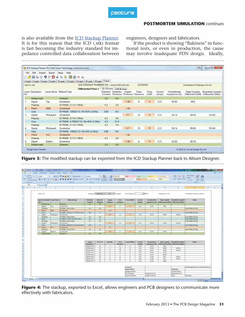
The less than desirable stackup in Figure 2 can be exported from Altium Designer (S09 to R13) into the ICD Stackup Planner to incorpo-rate dielectric materials and adjust the stackup for optimal performance. The stackup is then modified to give 50 ohms single-ended and 100 ohms differential impedance by moving the plane layers and adding dielectric materials from the Stackup Planner’s dielectric materials library.
Once modified, the stackup in Figure 3 can then be exported back to Altium Designer to also include impedance-controlled routing and differential rules. Plus, the stackup can also be exported to HyperLynx LineSim for pre-layout analysis, BoardSim for post-layout analysis, PADS and Allegro.
To promote communication with PCB fab-ricators, an Excel spreadsheet output (Figure 4)
feature
Figure 2:
POSTMORTEM SIMULATION continues
31
is also available from the ICD Stackup Planner. It is for this reason that the ICD (.stk) format is fast becoming the industry standard for im-pedance controlled data collaboration between
engineers, designers and fabricators.If the product is showing “flakiness” in func-
tional tests, or even in production, the cause may involve inadequate PDN design. Ideally,
POSTMORTEM SIMULATION continues
feature
Figure 3:
Figure 4:
32
issues like this should be resolved before a sin-gle chip has been placed on the board.
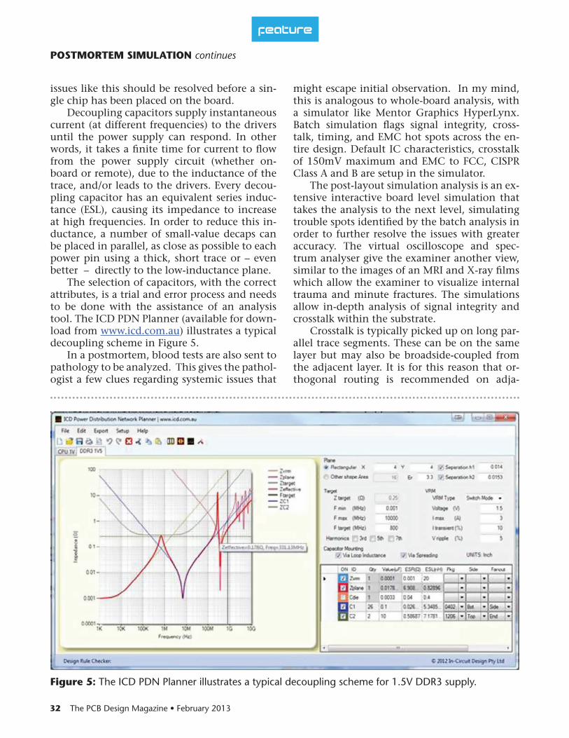
Decoupling capacitors supply instantaneous current (at different frequencies) to the drivers until the power supply can respond. In other words, it takes a finite time for current to flow from the power supply circuit (whether on-board or remote), due to the inductance of the trace, and/or leads to the drivers. Every decou-pling capacitor has an equivalent series induc-tance (ESL), causing its impedance to increase at high frequencies. In order to reduce this in-ductance, a number of small-value decaps can be placed in parallel, as close as possible to each power pin using a thick, short trace or – even better – directly to the low-inductance plane.
The selection of capacitors, with the correct attributes, is a trial and error process and needs to be done with the assistance of an analysis tool. The ICD PDN Planner (available for down-load from www.icd.com.au) illustrates a typical decoupling scheme in Figure 5.
In a postmortem, blood tests are also sent to pathology to be analyzed. This gives the pathol-ogist a few clues regarding systemic issues that
might escape initial observation. In my mind, this is analogous to whole-board analysis, with a simulator like Mentor Graphics HyperLynx. Batch simulation flags signal integrity, cross-talk, timing, and EMC hot spots across the en-tire design. Default IC characteristics, crosstalk of 150mV maximum and EMC to FCC, CISPR Class A and B are setup in the simulator.
The post-layout simulation analysis is an ex-tensive interactive board level simulation that takes the analysis to the next level, simulating trouble spots identified by the batch analysis in order to further resolve the issues with greater accuracy. The virtual oscilloscope and spec-trum analyser give the examiner another view, similar to the images of an MRI and X-ray films which allow the examiner to visualize internal trauma and minute fractures. The simulations allow in-depth analysis of signal integrity and crosstalk within the substrate.
Crosstalk is typically picked up on long par-allel trace segments. These can be on the same layer but may also be broadside-coupled from the adjacent layer. It is for this reason that or-thogonal routing is recommended on adja-
POSTMORTEM SIMULATION continues
feature
Figure 5:
33
POSTMORTEM SIMULATION continues
cent layers (between planes) to minimize the coupling area. Figure 6 shows this crosstalk on the 45-degree routes. It is recommend that seg-ments are only routed to a maximum of 500 mils in parallel or that the clearance is increased to at least 3x trace width to avoid coupling.
The next step in the analysis is to exam-ine timing: This is the heartbeat of the design. Irregular heartbeat can have catastrophic affects just as irregular timing can cause intermittent faults in a digital system. In the classic high-speed design flow, timing speci-fications and simulation results are compared to check skew and set and hold times to ensure ev-erything is operating like clockwork.
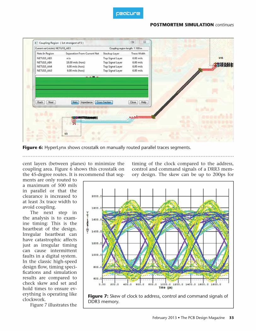
Figure 7 illustrates the
timing of the clock compared to the address, control and command signals of a DRR3 mem-ory design. The skew can be up to 200ps for
feature
Figure 6:
Figure 7:

34
DDR3-800. Also, the skew between data lanes and data strobes should be kept to less than 125ps and the eyes should be wide open. DDR3 is much easier to route, in fact, than DDR2 as leveling can be used to synchronize the delay of groups of signals. All critical signals are checked with the physical information that is obtained from the PCB data base (e.g., trace lengths, clearances, vias, etc.) to ensure that the design complies to specification.
ConclusionDeveloping the practice of performing a
postmortem analysis on every project – iden-tifying both the good and the bad – facilitates a culture of continuous improvement. Embed-ding a culture of ongoing, positive change in-side a project delivery organization is the best way to ensure long-term success. Postmortems are an important link in this chain of positive improvement.
Points to remember:
1. Ideally, the simulation should be done
during the design process to ensure design in-
tegrity.
2. A postmortem should be performed on
every project, creating a culture of continuous
improvement.
3. For a project that suffers from intermit-
tent flakiness, the postmortem can begin with
a thorough external examination – a second set
of eyeballs – looking for the obvious.
4. The PCB stackup can be the source
of problems that include impedance mis-
matches, signal integrity problems, crosstalk,
or emissions. As part of the stackup optimiza-
tion process, a PCB stackup can be exported
from several PCB environments to the ICD
Stackup Planner to incorporate dielectric mate-
rials and adjust the stackup for optimal perfor-
mance.
5. Once modified, the stackup can then be
exported back to the PCB environment or to
HyperLynx for signal integrity, crosstalk, and
EMC analysis. With Altium Designer, imped-
ance and differential routing rules can also be
incorporated into the export.
6. To improve communications with PCB
Fabricators, an Excel spreadsheet output is also
available.
7. The design of the PDN is another impor-
tant part of the conceptual design process, and
should be analyzed as part of a comprehensive
postmortem, as well.
8. Post-layout (board-level) analysis can find
systemic trouble spots in a design.
9. Crosstalk is typically picked up on long
parallel trace segments.
10. Interactive simulation takes the investi-
gation process deeper, including detailed signal
integrity analysis, as well as crosstalk and tim-
ing.
11. Timing is the heartbeat of the design.
Irregular timing can cause intermittent faults in
a digital system. PCBDESIGN
References1. Advanced Design for SMT – Barry Olney2. Beyond Design: Interactive Placement
and Routing Strategies – Barry Olney3. Beyond Design: Intro to Board-Level
Simulation and the PCB Design Process – Barry Olney
4. Beyond Design: Mixed Digital-Analog Technologies – Barry Olney
5. PCB Design Techniques for DDR, DDR2 & DDR3, Part 2 – Barry Olney
6. PCB Design Techniques for DDR, DDR2 & DDR3, Part 1 – Barry Olney
7. The ICD Stackup and PDN Planner can be downloaded from www.icd.com.au
All trademarks are registered trademarks of their respective owners. E&OE
POSTMORTEM SIMULATION continues
feature