srs trigger processor option status and plans
DESCRIPTION
SRS Trigger Processor Option Status and Plans. Sorin Martoiu (IFIN-HH). ATCA-SRS Status. First systems delivered IFIN-HH UPV and CERN (MAMMA Group) Beta firmware released New firmware will be released soon Integration with software under way. SRS ATCA card overview. - PowerPoint PPT PresentationTRANSCRIPT

SRS Trigger Processor OptionStatus and Plans
Sorin Martoiu (IFIN-HH)

2
ATCA-SRS Status• First systems delivered
– IFIN-HH– UPV and – CERN (MAMMA Group)
• Beta firmware released• New firmware will be released
soon• Integration with software under
way

3
SRS ATCA card overview
RTM I/O card: 2 x 8 SFP+ ports2 x Rj45 (DTCC)2 x NIM (SMA)
Blade main board: 2 x Virtex 6 FPGA (LX130/240)2 x DDR32 x mezzanine ports
2 x
Mez
zani
nes
ATCA Zone 2backplane connectors
ATCA zone 1 power connector
ATCA Zone 3RTM connector
RTM I/O card v2:(under design) 2 x 10GbE (SFP+)2 x 4 SFP+ ports2 x Rj45 (DTCC)2 x NIM (SMA)

4
ATCA-SRS Specifications
Full-mesh backplane connectivity• Board-to-board connections • 14 x 8 LVDS (13 x 9,6 Gbps – low latency))
Rear Transition Module • Optional connection to outside world• 2 x 8 GTX (2 x 40(50)Gbps)
– Ethernet, Infiniband, Slink,…– 2 x 10 GbE + 4 x SFP+ under design
• 2 x DTCC link (4xLVDS - RD51 specific data, trigger, clock and control link)
Hub Backplane Connection (CH0)• 4 x GTX versatile connection
– 2 x each FPGA– 4 x 1 (Master) FPGA
• Custom protocol (eg. HS-DTCC), 10GbE, Infiniband, …
• 40 GbE possible with V7 upgrade

5
• 8
8 GTX• 50 LVDS I/O • 16 SE • 2 LVDS CLKS (from PLL)
Power:2.5V3.3V12V M
anag
emen
t
Low Latency LinksMezzanine Interface
Samtec QTE/QSE Connector Samtec QTE/QSE Connector

6
Low Latency LinksOverview
Inter-FPGA link
• 8 x LVDS (upgradable)
• 2 x GTX
Full-mesh backplane connectivity• Board-to-board connections • 14 x 8 LVDS
Mezzanine interface
• 50 x LVDS
• 8 x GTX
Mezzanine interface
• 50 x LVDS
• 8 x GTX

7
Low Latency LinksTimings
Inter-FPGA link
• 8 x LVDS (upgradable)
~ 15 ns (using SelectIO circuitry)
Full-mesh backplane connectivity• 15 x 8 LVDS~ 15 ns (using SelectIO circuitry)
Mezzanine interface
• 50 x LVDS
~ 3 ns (eg. 320 MHz)
Mezzanine interface
• 50 x LVDS
~ 3 ns
*Measurements under way at IFIN-HH
8
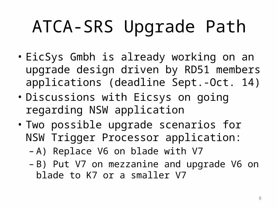
ATCA-SRS Upgrade Path
• EicSys Gmbh is already working on an upgrade design driven by RD51 members applications (deadline Sept.-Oct. 14)
• Discussions with Eicsys on going regarding NSW application
• Two possible upgrade scenarios for NSW Trigger Processor application:– A) Replace V6 on blade with V7– B) Put V7 on mezzanine and upgrade V6 on blade to K7
or a smaller V7

9
ATCA-SRS Trigger Processor
OPTO
OPO
OPTO
OPTOMEZZANINE
(V7)FPGA
OPTO
OPO
OPTO
OPTOMEZZANINE
(V7)FPGA
Track resultsTo/from
neighbor card
To monitoring switch (eg. 10GbE)
V7 – Track finding algorithm
K7/V7 – combine sTGC/MM results + Monitoring, Management, etc,.
To Sector Logic
OPTO
OPO
OPTO
OPTOMEZZANINE
(V7)FPGA
OPTO
OPO
OPTO
OPTOMEZZANINE
(V7)FPGA
Track resultsTo/from
neighbor card
To monitoring switch (eg. 10GbE)
V7 – Track finding algorithm & combine results +
To Sector Logic
10
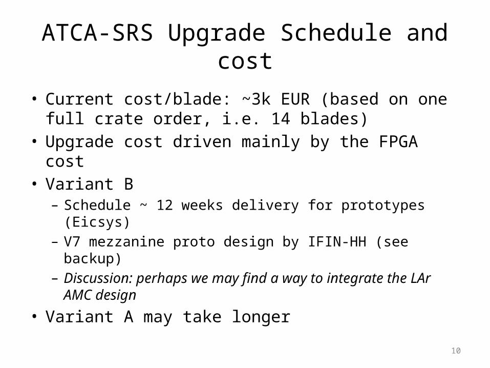
ATCA-SRS Upgrade Schedule and cost
• Current cost/blade: ~3k EUR (based on one full crate order, i.e. 14 blades)
• Upgrade cost driven mainly by the FPGA cost• Variant B
– Schedule ~ 12 weeks delivery for prototypes (Eicsys)– V7 mezzanine proto design by IFIN-HH (see backup)– Discussion: perhaps we may find a way to integrate the LAr
AMC design
• Variant A may take longer
11
Backup
12
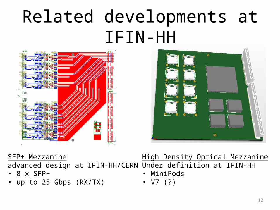
Related developments at IFIN-HH
SFP+ Mezzanineadvanced design at IFIN-HH/CERN• 8 x SFP+• up to 25 Gbps (RX/TX)
High Density Optical MezzanineUnder definition at IFIN-HH• MiniPods• V7 (?)