spin polarized current phenomena in magnetic tunnel junctionssnow.stanford.edu/thesis/gao.pdf ·...
TRANSCRIPT
SPIN POLARIZED CURRENT PHENOMENA IN MAGNETIC TUNNEL JUNCTIONS
A DISSERTATION
SUBMITTED TO THE DEPARTMENT OF APPLIED PHYSICS
AND THE COMMITTEE ON GRADUATE STUDIES
OF STANFORD UNIVERSITY
IN PARTIAL FULFILLMENT OF THE REQUIREMENTS
FOR THE DEGREE OF
DOCTOR OF PHILOSOPHY
Li Gao
September 2009

© Copyright by Li Gao 2009
All Rights Reserved
ii

I certify that I have read this dissertation and that, in my opinion, it is fully adequate in scope
and quality as a dissertation for the degree of Doctor of Philosophy.
_________________________________________________
(James S. Harris) Principal Advisor
I certify that I have read this dissertation and that, in my opinion, it is fully adequate in scope
and quality as a dissertation for the degree of Doctor of Philosophy.
_________________________________________________
(Stuart S. P. Parkin) co-Principal Advisor
I certify that I have read this dissertation and that, in my opinion, it is fully adequate in scope
and quality as a dissertation for the degree of Doctor of Philosophy.
_________________________________________________
(Walter A. Harrison)
Approved for the University Committee On Graduate Studies.
_________________________________________________
iii

iv
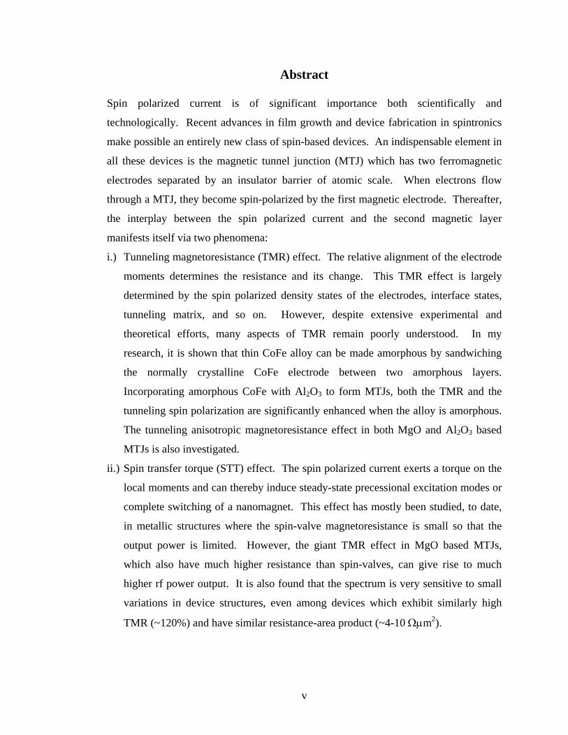
Abstract
Spin polarized current is of significant importance both scientifically and
technologically. Recent advances in film growth and device fabrication in spintronics
make possible an entirely new class of spin-based devices. An indispensable element in
all these devices is the magnetic tunnel junction (MTJ) which has two ferromagnetic
electrodes separated by an insulator barrier of atomic scale. When electrons flow
through a MTJ, they become spin-polarized by the first magnetic electrode. Thereafter,
the interplay between the spin polarized current and the second magnetic layer
manifests itself via two phenomena:
i.) Tunneling magnetoresistance (TMR) effect. The relative alignment of the electrode
moments determines the resistance and its change. This TMR effect is largely
determined by the spin polarized density states of the electrodes, interface states,
tunneling matrix, and so on. However, despite extensive experimental and
theoretical efforts, many aspects of TMR remain poorly understood. In my
research, it is shown that thin CoFe alloy can be made amorphous by sandwiching
the normally crystalline CoFe electrode between two amorphous layers.
Incorporating amorphous CoFe with Al O to form MTJs, both the TMR and the
tunneling spin polarization are significantly enhanced when the alloy is amorphous.
The tunneling anisotropic magnetoresistance effect in both MgO and Al O based
MTJs is also investigated.
2 3
2 3
ii.) Spin transfer torque (STT) effect. The spin polarized current exerts a torque on the
local moments and can thereby induce steady-state precessional excitation modes or
complete switching of a nanomagnet. This effect has mostly been studied, to date,
in metallic structures where the spin-valve magnetoresistance is small so that the
output power is limited. However, the giant TMR effect in MgO based MTJs,
which also have much higher resistance than spin-valves, can give rise to much
higher rf power output. It is also found that the spectrum is very sensitive to small
variations in device structures, even among devices which exhibit similarly high
TMR (~120%) and have similar resistance-area product (~4-10 Ωμm2).
v

vi

Acknowledgements
First of all, I am deeply grateful for Stuart Parkin’s supervision and support of my Ph.D.
work at the IBM Almaden Research Center. What I learned from him is far beyond
knowledge and skills, and I am greatly impressed by his intelligence, passion, and
innovation. I also really appreciate lots of help from him in my personal life. An
excellent physicist, a great man, I luckily worked with in one important phase of my life.
I would like to sincerely thank Coach for admitting me to Harris group, and
introducing me to the exciting field of spintronics. I especially appreciate his generous
support at the beginning of my studies at Stanford. I thank Coach for his kind and
persistent encouragement and help throughout all my Ph.D. years.
Special acknowledgements to Xin Jiang, without him many of my achievements are
impossible. Thanks to other members of Parkin group for various help, I am honored of
working with them: Masamitsu Hayashi, Rai Moriya, See-Hun Yang, Brian Hughes,
Mahesh Samant, Kevin Roche, Luc Thomas, Hyunsoo Yang, Christian Kaiser,
Nagaphani Aetukuri, Justin Brockman, Cheng-Han Yang, Guenole Jan, Andreas Ney,
Ruisheng Liu, Bastiaan Bergman, Roger Wang, Rekha Rajaram, and Joanna Lankester.
I thank Jonathan Sun for many stimulating discussions.
I acknowledge the help of Andrew Kellock for many RBS results, Philip Rice, Teya
Topuria, and Leslie Krupp for TEM images, Dolores Miller for XPS measurements, and
Charles Rettner for ebeam lithography.
I appreciate all the theoretical discussions with Dr. Don Nicholson, Prof. Evgeny
Tsymbal, Dr. John Burton, Prof. Walter Harrison, Prof. William Butler, Dr. Mairbek
Chshiev, and thank them for their calculations on my experimental results.
I also thank Prof. Walter Harrison for his willingness to be my reading committee
member, Prof. David Goldhaber-Gordon for chairing my oral defense, and Prof. Ian
Fisher for serving as an examiner.
All the administrative supports from Paula Perron, Gail Chun-Creech, Yvonne
Paxton, and Claire Nicholas are invaluable. Many thanks are also extended to all the
members in Harris group.
Finally, I would like to thank my parents, my wife, my parents-in-law, and my
sister’s family for years of support and encouragement. I am greatly indebted to them.
vii

viii

Table of Contents
Table of Contents
Abstract....................................................................................................................v
Acknowledgments .................................................................................................vii
Table of Contents....................................................................................................ix
List of Figures.........................................................................................................xi
Chapter 1: INTRODUCTION TO SPIN POLARIZED CURRENT AND SPINTRONICS..........1
Chapter 2: EXPERIMENTAL BACKGROUND...............................................................7
2.1 Spin Polarized Current in Magnetic Tunnel Junctions..........................8
2.1.1 Tunneling Magnetoresistance.................................................................8
2.1.2 Spin Transfer Torque...........................................................................11
2.2 Experimental Techniques ....................................................................14
2.2.1 Superconducting Tunneling Spectroscopy.............................................15
2.3 Device Preparation ..............................................................................18
2.3.1 Shadow Masked Devices .....................................................................18
2.3.2 Nano-Pillar Devices ............................................................................20
Chapter 3: ENHANCED TUNNELING MAGNETORESISTANCE FROM AMORPHOUS COFE
ALLOY...........................................................................................................27
3.1 Introduction .........................................................................................28
3.2 Materials and Methods ........................................................................29
3.3 Experimental Results...........................................................................33
3.3.1 Enhanced TMR from Amorphous CoFe................................................33
3.3.2 Increased TSP from Amorphous CoFe..................................................38
3.3.3 When CoFe beneath Al2O3...................................................................44
3.4 Discussion............................................................................................47
3.4.1 X-Ray Emission Spectroscopy .............................................................47
3.4.2 Band Structure Calculations.................................................................49
3.4.3 Explanation ........................................................................................51
ix
Table of Contents
3.5 Summary ..............................................................................................53
Chapter 4: TUNNELING ANISOTROPIC MAGNETORESISTANCE IN MAGNETIC TUNNEL
JUNCTIONS WITH 3D TRANSITION METALS ....................................................59
4.1 Introduction..........................................................................................60
4.2 Experiments and Results......................................................................61
4.2.1 Samples and Measurement Setup..........................................................61
4.2.2 TAMR Results ....................................................................................63
4.2.3 Inelastic Electron Tunneling Spectroscopy ............................................68
4.3 Discussion............................................................................................70
4.4 Other Results........................................................................................74
4.5 Summary ..............................................................................................79
Chapter 5: SPIN TRANSFER TORQUE INDUCED MICROWAVE EMISSION FROM MGO
BASED TUNNEL JUNCTIONS ...........................................................................83
5.1 Introduction..........................................................................................84
5.2 Samples and Experiments ....................................................................85
5.3 Experimental Results ...........................................................................88
5.3.1 Field and Current Induced Switching ....................................................88
5.3.2 STT Induced Microwave Emission .......................................................89
5.3.3 Sensitive Spectrum .............................................................................94
5.4 Discussion and Comment ....................................................................98
Chapter 6: CONCLUSIONS AND SUGGESTIONS FOR FURTHER RESEARCH ..............103
6.1 Conclusions........................................................................................104
6.2 Suggestions for Further Research ......................................................106
Appendix: LIST OF ACRONYMS ............................................................................107
x

List of Figures
List of Figures
Chapter 1: Introduction to Spin Polarized Current and Spintronics
Fig. 1.1 Classical illustration of electron spin as a small magnet with north pole
pointing to up or down. ...................................................................................2
Fig. 1.2 Diagram of the spin-resolved electronic structures for 4s and 3d bands in
Co. Red (or blue) is for spin-down (or spin-up). Numbers denote how many
electrons per Co atom are in the corresponding band. . ..................................3
Chapter 2: Experimental Background
Fig. 2.1 (a) Diagrammatic structure of a MTJ with an antiferromagnetic (AF) layer
grown underneath to provide exchange bias; (b) Typical magnetoresistance
loop of a MTJ device, the inset is the minor loop. The horizontal arrows
show the magnetic moments’ directions in the two electrodes, and the
vertical arrows denote the field sweeping directions.......................................9
Fig. 2.2 Illustration of the Jullière’s model in a magnetic tunnel junction for parallel
configuration (left) and antiparallel configuration (right). The current is
determined by the product of the density of filled states in one electrode and
the density of empty states in the other electrode. Parallel configuration
usually has lower resistance than that of antiparallel configuration, thus
resulting in a positive TMR effect. ................................................................11
Fig. 2.3 The thick electrode is pinned layer (PL), and the thin one is free layer (FL).
When electrons flow from PL to FL, due to spin transfer torque effect, it
favors parallel state (left); on the other hand, when electrons flow from FL to
PL, it favors antiparallel state. .......................................................................12
Fig. 2.4 (a) Geometric illustration of Landau-Lifshitz-Gilbert (LLG) equation with a
spin transfer torque term; (b) Dynamics of the magnetic moments in the free
layer (FL) when the damping term is larger, comparable, or smaller than the
spin-torque term with various magnitudes of spin polarized current.… .......13
Fig. 2.5 Comparison between the conventional MRAM (left) and STT-RAM (right).
Clearly, much simpler electronic architecture is proposed for STT-RAM than
the conventional MRAM...............................................................................14
xi
List of Figures
Fig. 2.6 Superconducting-ferromagnetic-metal tunneling. (a) BCS density of states
of a superconductor as a function of voltage in a magnetic field; (b)
Temperature-dependent kernels for each spin channel in the integral
expression for differential conductance; (c) Theoretical normalized
conductance for each spin channel (dotted and dashed curves) and the total
conductance (solid line). ................................................................................17
Fig. 2.7 Schematic of the sputtering system (left); Shadow masking is used to define
the electrodes and barriers (upper middle), and blank film is grown for
lithography (lower middle); Scanning electron microscopy (SEM) images for
some devices, respectively (right)..................................................................19
Chapter 3: Enhanced Tunneling Magnetoresistance from Amorphous CoFe Alloy
Fig. 3.1 High-resolution cross-section transmission electron microscopy images of
100 Ta/250 Ir22Mn78/4 Co49Fe21BB30/35 Co70Fe30/[44 Al2O3/tSCF SCF/100
CFB]5/50 Ta/50 Ru with tSCF of 15, 20, 30, 40, and 50 Å; (a) CFB=CFB30,
as deposited; (b) high magnification of a portion of (a), together with
diffractograms of the four regions indicated by black square outlines in the
figure. These regions are taken from (bottom to top) 20 Å SCF, 100 Å
CFB30, 30 Å SCF, and 100 Å CFB30: the amorphous to crystalline
transition as a function of thickness of the SCF layer is clearly revealed; (c)
CFB=CFB10 annealed at 260 °C. The thicknesses (in Å) of the SCF, Al2O3,
and CFB layers are labeled in green, yellow, and orange, respectively. .......31
Fig. 3.2 As-deposited all-metal sample, 100 Ta/250 Ir20Mn80/100 CFB30/[tSCF=5,
10, 15, …, and 40 SCF/100 CFB30]8/50 Ta/50 Ru. The thicknesses (in Å)
of the SCF, Al2O3, and CFB30 layers are labeled in green, yellow, and
orange, respectively. ......................................................................................32
Fig. 3.3 (a) Schematic of the magnetic tunnel junction structure; (b) Major and
minor (inset) TMR loops for CFB10 samples with tSCF = 10 and 60 Å. Blue
solid and red open circles denote results after the samples are annealed at
240 °C and 300 °C, respectively....................................................................34
Fig. 3.4 Dependence of TMR on the SCF thickness at various anneal temperatures
for CFB10 (solid circle) and CFB30 (open circle) samples.… .....................35
xii
List of Figures
Fig. 3.5 Dependence of Hc on the SCF thickness at various anneal temperatures for
CFB10 (upper) and CFB30 (lower) samples.................................................36
Fig. 3.6 Dependence of TMR on anneal temperature for CFB10 (upper) and CFB30
(lower) samples with tSCF = 20 Å (red circle) and 60 Å (blue circle). The
dashed lines are guides to the eye..................................................................37
Fig. 3.7 Typical experimental data from superconducting-tunneling-spectroscopy
from the tunnel junctions with structure, 45 Al95Si5/32 Al2O3/tSCF SCF/100
CFB10/50 Ta/50 Ru, at T ~ 0.250 K and H = 2.0 T; (a) tSCF = 25 Å, as-
deposited; (b) tSCF = 25 Å, annealed at 300 °C; (c) tSCF = 70 Å, as-deposited;
(d) tSCF = 70 Å, annealed at 300 °C. Open circles are experimental data and
solid lines are fits. Δ is the fitted Al95Si5 superconducting energy gap. .......40
Fig. 3.8 Dependence of TSP on the SCF thickness at various anneal temperatures
for both CFB10 and CFB30 samples.............................................................41
Fig. 3.9 Anneal temperature dependence of TSP and resistance for both normal
(solid symbols, 45 Al95Si5/32 Al2O3/25 SCF/100 CFB30/50 Ta/50 Ru) and
inverted (open symbols, 100 Ta/250 Ir24Mn76/4 Co49Fe21BB30/35 Co70Fe30/28
Al2O3/40 Al95Si5/33 MgO) STS samples. The tunnel barrier Al2O3 was
grown by reactive sputtering in an O2-Ar mixture with (triangles) or without
an additional atomic oxygen treatment (30 or 60 seconds) after deposition.
Oxygen concentrations in the sputter gas mixture of 7% (circles and
triangles), 9% (square), and 11% (diamond) were used................................42
Fig. 3.10 Atomic force microscopy images (AFM) for Al2O3 barriers (a) in normal
structure, 45 Al95Si5/32 Al2O3; (b) in inverted structure, 100 Ta/250
Ir22Mn78/6 Co40Fe40BB20/35 Co70Fe30/32 Al2O3. Both the barriers were
deposited in the optimal condition with an Ar-O2 (93/7) mixture. Clear grains
with RMS ~ 0.395 nm in the normal structure and much smoother surface
with RMS ~ 0.190 nm in the inverted structure were observed. ...................43
Fig. 3.11 (a) Schematic diagram of the magnetic tunnel junction structure with the
SCF layer underneath the tunnel barrier; (b) Major and minor (inset) TMR
loops for tSCF = 15 Å. Black open and violet solid circles denote loops for an
xiii
List of Figures
as-deposited device and for the same device after an anneal at 260 °C,
respectively. ...................................................................................................44
Fig. 3.12 Dependence of TMR on the SCF thickness at various anneal temperatures
for the samples with CFB20 beneath Al2O3. .................................................46
Fig. 3.13 High-resolution cross-section transmission electron microscopy images
for (a) 100 Ta/250 Ir22Mn78/4 Co49Fe21BB30/5 Co70Fe30/[60 CFB20/tSCF
SCF/44 Al2O3]6 with tSCF =10, 15, 20, 30,40 and 50 Å (10 and 50 not
shown); (b) same sample as in (a) after an anneal at 260 °C. In both images,
the thicknesses of SCF, Al2O3, and CFB20 are labeled in green, yellow, and
orange, respectively. ......................................................................................47
Fig. 3.14 Fe L3 and Co L3 XES spectra as a function of the SCF thickness for 50
Ta/18 Al2O3/[tSCF SCF/20 CFB20], or 71 Co70Fe30, or 62 CFB20/10 Al2O3.
The thicknesses of CoFe (CoFeB) are shown in green (orange). The Fe and
Co 2p3/2 binding energies relative to the Fermi level are taken to be 707 eV
and 778 eV, as indicated by the dark-yellow dashed-dotted lines. ................48
Fig. 3.15 Spin-resolved s- and d- partial density of states for Fe and Co in
amorphous (blue and navy) and bcc crystalline (red and pink) Co70Fe30 alloy
structures. .......................................................................................................50
Fig. 3.16 Spin moment of each atom in the computational ensemble for amorphous
or bcc crystalline Co70Fe30. The horizontal axis indicates the label of the
individual Fe and Co atoms in the calculations. ............................................51
Chapter 4: Tunneling Anisotropic Magnetoresistance in Magnetic Tunnel Junctions
with 3d Transition Metals
Fig. 4.1 Schematic diagram of the TAMR measurement setup. Mixer adds the dc
bias voltage and a small ac voltage together, and applies the total voltage
across the tunnel junction. Lock-in amplifier is used to measure the dynamic
resistance at various dc bias voltages.............................................................62
Fig. 4.2 The bias dependence of differential conductance for the MgO (red line) and
Al2O3 (gray line) MTJs in a perpendicular field of 7 T at 10 K. The inset
shows the bias dependence of the differential TMR at 10 K.........................63
xiv

List of Figures
Fig. 4.3 Typical angular dependence of dV/dI curves for CoFe/MgO/CoFe,
CoFe/Al2O3/CoFe, and Al/MgO/Al at zero bias in a field of 7 T at 10 K.....64
Fig. 4.4 Normalized RD vs. θ curves (symbols) at various bias voltages for (a) MgO
and (b) Al2O3 MTJs. The data are displaced vertically for clarity. The solid
lines are fits using Eqs. (1) and (2).…...........................................................65
Fig. 4.5 (a) and (b) Contour plots of RD as a function of bias and angle for the MgO
and Al2O3 MTJs; (c) and (d) Corresponding contour plots of dc resistance. 67
Fig. 4.6 (a) and (b) Fitting parameters A2/A0 (solid circles) and A4/A0 (open
squares) as a function of bias for the MgO and Al2O3 MTJs. .......................68
Fig. 4.7 IETS data for the CoFe/MgO/CoFe (red line) and CoFe/Al2O3/CoFe (gray
line) MTJs after linear background subtraction. The inset shows the original
data.................................................................................................................70
Fig. 4.8 Angular dependence of the interface DOS of the majority band (in arbitrary
units) for several energies E near the resonant energy Er = −0.4 eV. Energies
are given in eV. The majority band has width 4 eV and is centered at 0.6 eV.
The width of the resonant state γ0 = 10 meV, and the spin-orbit coupling
parameter λ = 50 meV. ..................................................................................71
Fig. 4.9 Bias dependence of differential conductance for CoFe/MgO/CoFe,
CrMo/MgO/CoFe, CoFe/MgO/CrMo, and CrMo/MgO/CrMo tunnel
junctions. The insets show the I-V curves of the tunnel junctions. The
measurements were taken at 10 K in a perpendicular field of 7 T. ...............75
Fig. 4.10 Contour plots for the angular dependence of normalized dc resistance at
10 K in a field of 7 T at various bias voltages for (a) CoFe/MgO/CoFe, (b)
CrMo/MgO/CoFe, (c) CoFe/MgO/CrMo, and (d) CrMo/MgO/CrMo tunnel
junctions.........................................................................................................76
Fig. 4.11 Angular dependence of normalized resistance at 10 K in a field of 7 T at
various bias voltages for (a) CoFe/MgO/0 CoFe/CrMo, (b) CoFe/MgO/5
CoFe/CrMo, (c) CoFe/MgO/10 CoFe/CrMo, and (d) CoFe/MgO/15
CoFe/CrMo tunnel junctions. Curves are displaced vertically for clarity. ...77
Chapter 5: Spin Transfer Torque Induced Microwave Emission from MgO Based
Tunnel Junctions
xv

List of Figures
Fig. 5.1 Schematic illustration of the measurement setup for the detection of spin
transfer torque induced microware emission. ................................................86
Fig. 5.2 Transmission coefficient of microwave signals at various frequencies in the
transmission line used in the setup.................................................................87
Fig. 5.3 Circuit model of the measurement setup for the detection of spin transfer
torque induced microware emission, where Rsub is the resistance of Si
substrate underneath the electrodes, Cpad is the capacitance between electrode
and Si substrate, RMTJ is the resistance of MTJ, Coverlap is the overlap
capacitance between top contact and bottom contact which is minimized by
an extended finger..........................................................................................87
Fig 5.4 Fig 5.4 (a) R vs. H at bias voltages of 0.01, 0.50, and -0.50 V; (b) R vs. V in a
field of 530 Oe. Positive voltage corresponds to electrons flowing from pinned
layer to free layer..............................................................................................89
Fig. 5.5 Typical spectra corresponding to ±0.5 V with various fields applied along
easy axis. With large positive fields MTJ is in AP state, and with large
negative fields in P state as shown by magnetoresistance loop. ....................90
Fig. 5.6 Contour plots of spectra corresponding to ±0.5 V with various fields
applied along easy axis. Dotted white lines divide plots into P and AP state.
Black downward arrow on right shows the field sweeping direction.
Colorbar shows microwave power level in the unit of nV/Hz0.5.. .................91
Fig 5.7 Field dependence of peak frequency (open circle) and FWHM (solid
triangle) at (a) 0.50 V and (b) -0.5 V. ............................................................91
Fig. 5.8 (a) Frequency f, (b) FWHM linewidth Δf, and (c) integrated power P versus
bias voltage for the two excitation modes in antiparallel state with a magnetic
field of 236 Oe applied along easy axis. ........................................................93
Fig 5.9 (a) Field switching and (b) current induced switching of two nominally
identical devices. Magnetoresistance loops are measured at 0.01 V, and
voltage switching loops are obtained with magnetic fields applied to cancel
the dipolar coupling, or the offset field in (a), respectively. Red (blue)
curves are for Device I (II).............................................................................95
xvi
List of Figures
Fig 5.10 Microwave emission spectra for Device I (a) and II (b) at ±0.5 V with
various fields applied along easy axis. Dotted white lines divide plots into P
and AP state. Colorbar shows microwave power level in the unit of
nV/Hz0.5. Field sweeping direction is always from positive from negative. 96
Fig. 5.11 Influence of over-etching time after Co/Mn crossover in secondary ion
mass spectroscopy (SIMS) on resistance RP, TMR, coercivity Hc, and dipolar
coupling field Hoffset. ......................................................................................97
xvii

List of Figures
xviii
Chapter 1
Chapter 1
INTRODUCTION: SPIN POLARIZED CURRENT AND SPINTRONICS
- 1 -

Chapter 1
As well as mass and charge, an electron has another intrinsic property, i.e. spin angular
momentum, or simply spin. In quantum mechanics, spin is a fundamental property of
atomic nuclei and elementary particles, and is an important intrinsic degree of freedom.
Although as the name indicates spin was originally thought of particles spinning around
their own axis, it had been shown by Dirac that electron spin arises naturally within
relativistic quantum mechanics. The component of electron spin measured along any
direction can only take on the values,
, 1z zs s / 2= ±
Namely, in a classical picture, electron spin can only point to up or down along a
magnetic field which can be vividly illustrated by a small magnet with its north pole
pointing to up or down as shown in Fig. 1.1. The intrinsic magnetic dipole moment
associated with such a spin in an electron is very close to a universal constant called the
Bohr magneton, ( ) ( )23 2 200.927 10 / 0.927 10 /2B
e
e J T or A m erg Oem
μ − −= = × ⋅ = × .
Fig. 1.1 Classical illustration of electron spin as a small magnet with north pole pointing to up or down.
In normal materials, such as Cu, Ag, etc., spin-up and -down electrons are equally
populated and randomly distributed in an equilibrium state. However, in some solids
due to the quantum mechanical exchange interaction, electron spins are aligned
spontaneously, resulting in unequal numbers of spin-up and -down electrons, therefore
ferromagnetic materials are formed, such as Co, Fe, Ni, and many of their alloys. In
these ferromagnetic materials, spin-resolved electronic structures show the band
- 2 -

Chapter 1
difference between the spin-up and -down electrons, as illustrated in Fig. 1.2, and the
asymmetry in density of states (DOS) at Fermi energy gives rise to most of the spin
related transport phenomena. When an unpolarized flow of electrons pass through a
normal metal, because of the identity between the bands for spin-up and -down
electrons, they experience the same scattering rate regardless of the spin, and the
emergent current still remains unpolarized. However, when they flow through a
ferromagnetic material, spin-up electrons may encounter less scattering, or may have
smaller effective mass, compared to spin-down electrons, so the conductivity due to the
majority spin channel would be higher. Then, a spin polarized current would emerge
from the ferromagnetic material[1].
Fig. 1.2 Diagram of the spin-resolved electronic structures for 4s and 3d bands in Co. Red (or blue) is for spin-down (or spin-up). Numbers denote how many electrons per Co atom are in the corresponding band.
Such a spin polarized current is of significant importance both scientifically and
technologically because it can be manipulated either via electron charge or spin, instead
of electron charge only in conventional electronics[2]. Since the discovery of the giant
magnetoresistance (GMR) effect in 1980’s[3-5], spin-electronics (spintronics) using
electron spin to control the current, has stimulated great interest in both the academic
and industrial fields. Astonishing achievements have been obtained, especially in data
storage applications. A few years later, due to the advances in the thin film growth and
- 3 -

Chapter 1
device fabrication, an even more significant effect, called the tunneling
magnetoresistance (TMR) effect, was observed at room temperature in magnetic
tunneling junctions (MTJs)[6-9]. Because of their huge TMR and high resistance,
MTJs promise attractive applications in magnetic field sensor and magnetic random
access memory (MRAM) in very small scale of solid-state circuitry[2]. Read heads
with MTJs in hard disk are commercially available, and there are many ongoing efforts
to realize MRAM. This new type of memory has all the key desirable attributes
required by the ever growing demand for storing and processing the explosive amount
of information, such as fast access times, non-volatility, lower power-consumption, and
high density. Moreover, from the perspective of physics, the quantum mechanical
tunneling process in MTJs is not only very interesting but also extremely complicated,
and many issues about it remain poorly understood[10].
The focus of the research in this dissertation is to deepen the understanding of the
spin dependent tunneling effect in MTJs. A brief background in MTJs is provided in
Chapter 2. It is first shown in Chapter 3 that the normally crystalline CoFe can be made
amorphous when sandwiched between two amorphous layers, and when this amorphous
CoFe is incorporated as an electrode in MTJs it gives rise to an enhanced TMR
compared to its crystalline counterpart. The tunneling anisotropic magnetoresistance
(TAMR) effect is investigated in conventional MTJs in Chapter 4, and it is found that
the angular dependence of the TAMR effect shows complex two-fold and four-fold
symmetry evolution with bias voltage. Chapter 5 is devoted to the studies of the current
induced switching and microwave emission from MTJs due to the spin transfer torque
effect. Chapter 6 provides a summary of the dissertation and some suggestions for
future research.
- 4 -

Chapter 1
REFERENCES:
[1] R. C. O'Handley, "Modern Magnetic Materials: Principles and Applications,"
(John Wiley & Sons, 2000).
[2] S. Parkin, X. Jiang, C. Kaiser, A. Panchula, K. Roche, and M. Samant,
"Magnetically Engineered Spintronic Sensors and Memory," Proc. IEEE 91, 661
(2003).
[3] M. N. Baibich, J. M. Broto, A. Fert, F. N. Van Dau, F. Petroff, P. Etienne, G.
Creuzet, A. Friederich, and J. Chazelas, "Giant Magnetoresistance of
(001)Fe/(001)Cr Magnetic Superlattices," Phys. Rev. Lett. 61 (21), 2472 (1988).
[4] G. Binasch, P. Grunberg, F. Saurenbach, and W. Zinn, "Enhanced
magnetoresistance in layered magnetic structures with antiferromagnetic
interlayer exchange," Phys. Rev. B 39 (7), 4828 (1989).
[5] S. S. P. Parkin, N. More, and K. P. Roche, "Oscillations in exchange coupling
and magnetoresistance in metallic superlattice structures: Co/Ru, Co/Cr, and
Fe/Cr," Phys. Rev. Lett. 64 (19), 2304 (1990).
[6] M. Julliere, "Tunneling between ferromagnetic films," Phys. Lett. A 54, 225
(1975).
[7] J. S. Moodera, L. R. Kinder, T. M. Wong, and R. Meservey, "Large
Magnetoresistance at Room Temperature in Ferromagnetic Thin Film Tunnel
Junctions," Phys. Rev. Lett. 74, 3273 (1995).
[8] S. S. P. Parkin, C. Kaiser, A. F. Panchula, P. Rice, M. G. Samant, S.-H. Yang,
and B. Hughes, "Giant tunneling magnetoresistance at room temperature with
MgO (100) tunnel barriers," Nature Materials 3, 862 (2004).
[9] S. Yuasa, T. Nagahama, A. Fukushima, Y. Suzuki, and K. Ando, "Giant room-
temperature magnetoresistance in single-crystal Fe/MgO/Fe magnetic tunnel
junctions," Nature Materials 3, 868 (2004).
[10] E. Y. Tsymbal, O. N. Mryasov, and P. R. LeClair, "Spin-dependent tunnelling in
magnetic tunnel junctions," J. Phys. C: Condens. Matter 15, R109 (2003).
- 5 -

Chapter 1
- 6 -

Chapter 2
Chapter 2
EXPERIMENTAL BACKGROUND
- 7 -
Chapter 2
2.1 SPIN POLARIZED CURRENT IN MAGNETIC TUNNEL JUNCTIONS
Magnetic tunnel junctions (MTJs) are sandwiched heterostructures, composed of two
ferromagnetic electrodes and an ultrathin insulator barrier in between, and present many
interesting phenomena that are important for both the exploration of underlying physics
and the applications in technology[1]. When electrons flow through a MTJ, they
become spin-polarized by the first magnetic electrode. Thereafter, the interplay
between the spin-polarized current and the second magnetic layer manifests itself via
two effects, i.e. tunneling magnetoresistance effect and spin transfer torque effect. In
the current section of this chapter, brief reviews will be given on these two interesting
effects.
2.1.1 Tunneling Magnetoresistance
The resistance of a MTJ depends on the relative alignment of the magnetic moments in
the ferromagnetic electrodes. Usually, when the moments are parallel the tunneling
resistance is low; when anti-parallel, the resistance is high, thus giving rise to a
tunneling magnetoresistance (TMR) effect,
100%AP P
P
R RTMRR−
= × ,
where RAP and RP are the resistances for the parallel and anti-parallel configurations. A
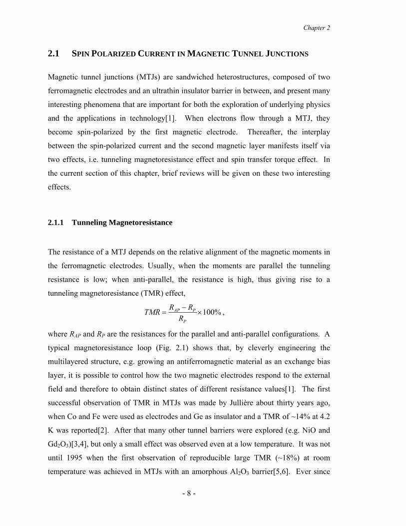
typical magnetoresistance loop (Fig. 2.1) shows that, by cleverly engineering the
multilayered structure, e.g. growing an antiferromagnetic material as an exchange bias
layer, it is possible to control how the two magnetic electrodes respond to the external
field and therefore to obtain distinct states of different resistance values[1]. The first
successful observation of TMR in MTJs was made by Jullière about thirty years ago,
when Co and Fe were used as electrodes and Ge as insulator and a TMR of ~14% at 4.2
K was reported[2]. After that many other tunnel barriers were explored (e.g. NiO and
Gd2O3)[3,4], but only a small effect was observed even at a low temperature. It was not
until 1995 when the first observation of reproducible large TMR (~18%) at room
temperature was achieved in MTJs with an amorphous Al2O3 barrier[5,6]. Ever since
- 8 -
Chapter 2
then, MTJs have aroused considerable interest due to their potential applications in
spintronic devices, such as high-performance solid-state magnetic random access
memories (MRAM) and magnetic sensors[1].
Pinned FM
Free FM
AF -100 -50 0 500
20
40
60
80
-800 -600 -400 -200 0 2000
20
40
60
80
H (Oe)
TMR
(%)
TMR
(%)
H (Oe)
(a) (b)
Fig. 2.1 (a) Diagrammatic structure of a MTJ with an antiferromagnetic (AF) layer grown underneath to provide exchange bias; (b) Typical magnetoresistance loop of a MTJ device, the inset is the minor loop. The horizontal arrows show the magnetic moments’ directions in the two electrodes, and the vertical arrows denote the field sweeping directions.
Over the past ten years, most of the research in spin dependent tunneling has
focused on MTJs with an Al2O3 tunnel barrier[7-9]. Although intensive efforts have
been made in such MTJs, the maximum TMR only reached about 70%[10,11].
Meanwhile, extensive theoretical and experimental work has been carried out to
increase the TMR by incorporating exotic oxide or half-metal layers into MTJs[12-15],
and studying crystalline tunneling barriers[16,17]. Butler et al. carried out first-
principles calculations of tunneling conductance and magnetoresistance in epitaxial
Fe/MgO/Fe sandwiches[16]. They revealed that tunneling conductance depends
strongly on the symmetry of the Bloch states in the electrodes and of the evanescent
states in the barrier, thus Bloch states of different symmetry decay at different rates
within the barrier. The state, due to its “s-character”, decays slowest among all the
states and can make a significant contribution to the tunneling conductance. Because
the state only occurs at the Fermi level for the majority band, it behaves much like a
“half-metal”. Giant TMR was expected in bcc Fe/MgO/Fe, CoFe/MgO/CoFe, and
Co/MgO/Co tunneling junctions. Experimental results of TMR above ~200% were first
1Δ
1Δ
- 9 -

Chapter 2
reported by Parkin et al. and Yuasa et al. respectively[18,19]. Room temperature TMR
results of about 600% in MgO based tunnel junctions have also been obtained
recently[20].
For high-quality Al2O3 tunnel junctions, the magnitude of the TMR at low bias can
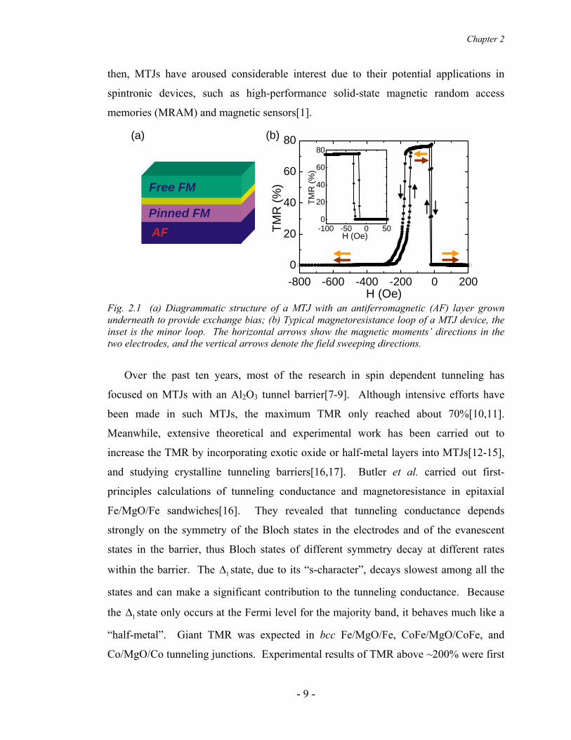
be well understood within the framework of Jullière’s model, 1 2
1 2
21
PPTMRPP
=−
, where
P1, P2 are the spin polarization of the two electrode materials and they can be well
derived from the ferromagnet/insulator/superconducting tunnel junctions first
introduced by Meservy and Tedrow[21]. In this model, it is assumed that during the
tunneling process, spin is conserved, namely no spin-flipping occurs. The conductance
in each channel is thus proportional to the tunneling probability, which is determined by
Fermi’s golden rule (Fig. 2.2). However, such a quantitative comparison is not always
straightforward. For example, TMR is extremely sensitive to the interface between the
electrode and barrier in realistic systems[22,23]. In MgO based MTJs, due to coherent
tunneling effect, the physics of the spin dependent tunneling effect is far beyond this
oversimplified model. Given the simplicity of the model, Slonczewski calculated an
approximate expression of the TMR of free electrons tunneling through a square barrier
based on the Landauer-Büttiker formalism[24]. Tsymbal et al. studied the interface
dependence of the tunneling conductance[23]. For the coherent tunneling through a
crystalline system many theoretical studies emerged together with the experimental
achievements in MgO based tunnel junctions[16-19].
In conventional MTJs, TMR always decreases with applied bias voltage. The
voltage at which the magnitude decreases to half of the low bias value is called V1/2,
usually around 0.5 V for high quality Al2O3 or MgO based MTJs with transition metal
electrodes[11,19]. The TMR decrease mainly comes from the much greater resistance
drop in the anti-parallel (AP) state with bias voltage compared to the parallel (P) state.
One mechanism for the decrease in TMR as a function of bias is the interface magnon
excitation[25]. Another is the presence of defect states within the tunnel barrier, which
may allow an increase amount of defect-state-assisted tunneling and dilute the spin
polarization of the tunneling current at elevated bias voltage[26,27].
- 10 -
Chapter 2
E E
NS N SE F E
F
EF
EF
e e
FM FMF FI I
M MM M
Ima ImajImin Imin
21 1 2AP N NI N N↓ ↓↑ ↑↑ ↑ ∝ +1 2 1 2
PI NN N N↓ ↓∝ +
Fig. 2.2 Illustration of the Jullière’s model in a magnetic tunnel junction for parallel configuration (left) and antiparallel configuration (right). The current is determined by the product of the density of filled states in one electrode and the density of empty states in the other electrode. Parallel configuration usually has lower resistance than that of antiparallel configuration, thus resulting in a positive TMR effect.
2.1.2 Spin Transfer Torque
Spin transfer torque (STT) effect was first theoretically studied by Slonczewski and
Berger in 1996[28,29]. When a spin-polarized current pass through a non-collinear thin
magnetic layer, due to the conservation of the spin momentum via exchange interaction,
the transverse component of the spin in the flowing electrons can be transferred to the
conduction electrons in the small magnet. Depending on the direction of electron flow
and the magnetic configuration, this spin-polarized current favors either the P state or
AP state (Fig. 2.3). The electrode of smaller thickness, which can be switched, is called
the free layer (FL); in contrast, the other electrode, which is usually thicker and
exchange biased, is called pinned layer (PL). Such a STT induced magnetization
reversal is a relatively new phenomenon, and it is observable only in magnetic
structures smaller than 100-200 nm[30-32]. A macro-spin model treats a nanomagnet
with the assumption that its internal magnetic degrees of freedom are frozen, so that the
- 11 -

Chapter 2
dynamics of macro-spin can be phenomenologically described by the following
Landau-Lifshitz-Gilbert (LLG) equation with an extra STT term[33,34]:
( ) ( ) ( )efft tm m H m m J m m Mγ α β∂ = × − ×∂ + × ×
where γ is the gyromagnetic ratio, α the damping coefficient, β the coefficient for the
STT which depends on both the spin polarization and the geometric configuration
between the incoming spin and the local moments in the FL, and J the current density.
Fig. 2.3 The thick electrode is pinned layer (PL), and the thin one is free layer (FL). When electrons flow from PL to FL, due to spin transfer torque effect, it favors parallel state (left); on the other hand, when electrons flow from FL to PL, it favors antiparallel state.
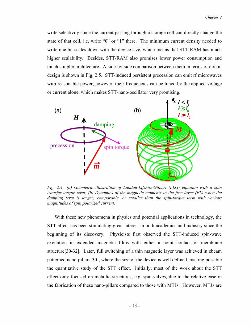
The competition between the damping term and the spin torque term is illustrated in
Fig. 2.4. When J is small and the spin torque term less than the damping term, the
dynamics damp out into an equilibrium state. When the spin torque is large enough that
it overcomes the intrinsic damping, effective damping coefficient becomes negative, the
deviation from the equilibrium state is amplified and the magnetic moments are
switched, which can be detected by a resistance change in the magnetic sandwiched
structure, e.g. MTJs or spin-valves[30,35,36]. When J and H satisfy certain conditions,
persistent precession of the magnetization can be obtained at a frequency of several
GHz. When the precession occurs, the angle between the magnetic moments in the FL
and PL changes rapidly. Due to the magnetoresistance effect, it gives rise to a
resistance change at high frequency; therefore a dc current/voltage induced rf
microwave emission can be observed in the device[32,37-42].
Since the STT can change the magnetic state of a small magnet by locally injecting
a spin polarized current, it promises a better writing scheme than that used in
conventional magnetic random access memory (MRAM). The STT-RAM has excellent
mM M m
- 12 -
Chapter 2
write selectivity since the current passing through a storage cell can directly change the
state of that cell, i.e. write “0” or “1” there. The minimum current density needed to
write one bit scales down with the device size, which means that STT-RAM has much
higher scalability. Besides, STT-RAM also promises lower power consumption and
much simpler architecture. A side-by-side comparison between them in terms of circuit
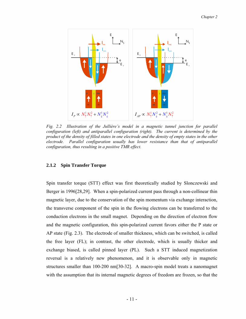
design is shown in Fig. 2.5. STT-induced persistent precession can emit rf microwaves
with reasonable power, however, their frequencies can be tuned by the applied voltage
or current alone, which makes STT-nano-oscillator very promising.
Fig. 2.4 (a) Geometric illustration of Landau-Lifshitz-Gilbert (LLG) equation with a spin transfer torque term; (b) Dynamics of the magnetic moments in the free layer (FL) when the damping term is larger, comparable, or smaller than the spin-torque term with various magnitudes of spin polarized current.
With these new phenomena in physics and potential applications in technology, the
STT effect has been stimulating great interest in both academics and industry since the
beginning of its discovery. Physicists first observed the STT-induced spin-wave
excitation in extended magnetic films with either a point contact or membrane
structure[30-32]. Later, full switching of a thin magnetic layer was achieved in ebeam
patterned nano-pillars[30], where the size of the device is well defined, making possible
the quantitative study of the STT effect. Initially, most of the work about the STT
effect only focused on metallic structures, e.g. spin-valves, due to the relative ease in
the fabrication of these nano-pillars compared to those with MTJs. However, MTJs are
damping
spin torque precession
H (a) (b)
m
- 13 -
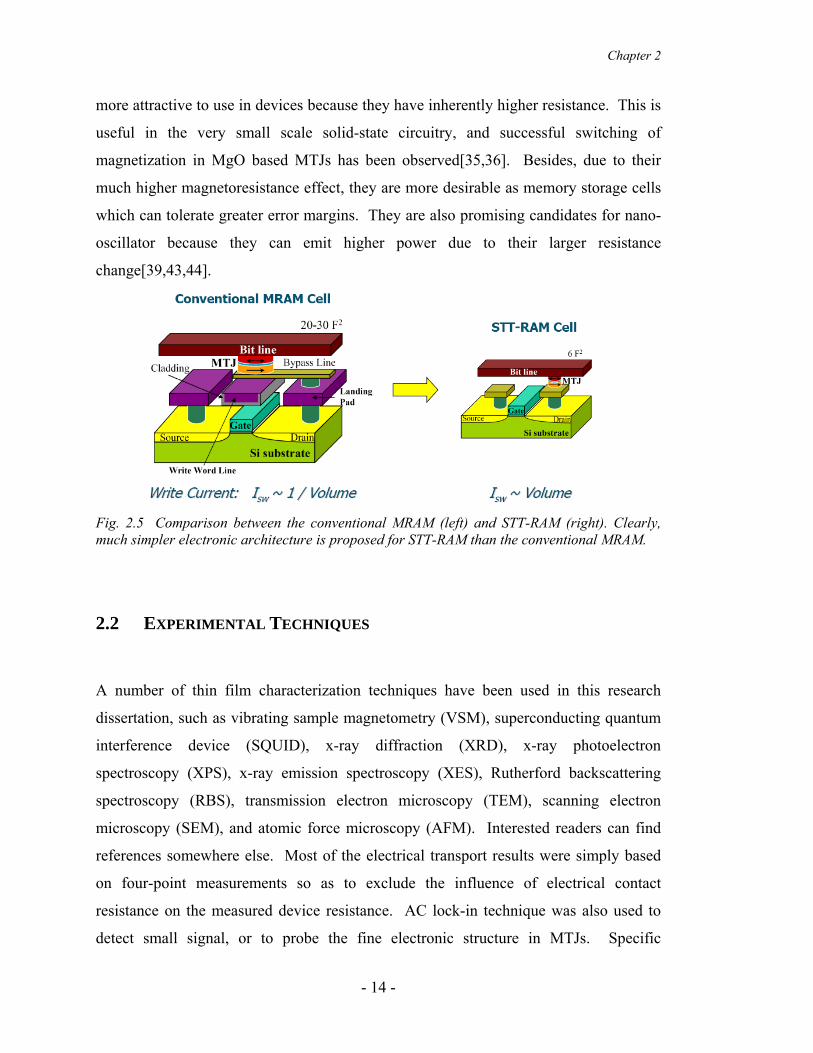
Chapter 2
more attractive to use in devices because they have inherently higher resistance. This is
useful in the very small scale solid-state circuitry, and successful switching of
magnetization in MgO based MTJs has been observed[35,36]. Besides, due to their
much higher magnetoresistance effect, they are more desirable as memory storage cells
which can tolerate greater error margins. They are also promising candidates for nano-
oscillator because they can emit higher power due to their larger resistance
uch simpler electronic architecture is proposed for STT-RAM than the conventional MRAM.
.2 EXPERIMENTAL TECHNIQUES
change[39,43,44].
ig. 2.5 Comparison between the conventional MRAM (left) and STT-RAM (right). Clearly,F
m
2
A number of thin film characterization techniques have been used in this research
dissertation, such as vibrating sample magnetometry (VSM), superconducting quantum
interference device (SQUID), x-ray diffraction (XRD), x-ray photoelectron
spectroscopy (XPS), x-ray emission spectroscopy (XES), Rutherford backscattering
spectroscopy (RBS), transmission electron microscopy (TEM), scanning electron
microscopy (SEM), and atomic force microscopy (AFM). Interested readers can find
references somewhere else. Most of the electrical transport results were simply based
on four-point measurements so as to exclude the influence of electrical contact
resistance on the measured device resistance. AC lock-in technique was also used to
detect small signal, or to probe the fine electronic structure in MTJs. Specific
- 14 -

Chapter 2
experimental setups for the different experiments will be discussed later in the
respective chapters. However, one special technique, i.e. superconducting tunneling
spectroscopy, will be described in details in this section due to its theoretical and
xperimental complexities.
.2.1 Superconducting Tunneling Spectroscopy
3d
tran
nneling electrons from left electrode to
right electrode at energy E and vice versus are,
e
2
Spin polarization is a crucial metric for all spin related phenomena. It can be probed by
a variety of techniques, such as photoemission[45], point contact Andreev
reflection[46], and superconducting tunneling spectroscopy (STS)[21]. Regarding the
spin dependent tunneling effect in MTJs, STS is the most reliable and relevant
technique to determine the tunneling spin polarization (TSP). In this technique, TSP is
measured from a tunnel junction with an electrode of the interested material and a
counter electrode of a superconducting material. Slightly doped aluminum with copper
or silicon is commonly used as the superconducting electrode, where the doping can
increase the critical temperature Tc of the superconductor. With a large field applied in
the film plane, the superconducting electrode works as an analyzer for the spin-
polarized current. This technique was first developed by Meservey and Tedow, and has
been used to measure many ferromagnetic and ferromagnetic materials including
sition metals and their alloys and some rare-earth metal based alloys[21,47,48].
When a bias voltage is applied across the tunnel junction, the initially aligned Fermi
levels in the two electrodes are shifted, therefore giving rise to a tunneling current.
According to Fermi’s golden rule, the current that is directly correlated with the
tunneling probability, is determined by the product of the density of filled states of a
given energy in one electrode and the density of empty states at the same energy in the
other electrode. By this rule, the currents of tu
( ) ( ) ( ) ( ) ( )( ) ( ) ( ) ( ) (
1 2
1 2
, ~ 1
, ~ 1 )I V E N E eV N E f E eV f E
I V E N E eV N E f E eV f E+
−
+ + −⎡ ⎤⎣ ⎦+ − +⎡ ⎤⎣ ⎦
- 15 -
Chapter 2
respectively, where V is the applied voltage, N1,2 are the density of states of the two
electrodes, and f is the Fermi function. Thus the total current I, given by
( ) ( ), ,I V E I V E dE+∞
+ −−∞−∫ , is equal to,
( ) ( ) ( ) ( ) ( )1 2~I V N E eV N E f E eV f E+∞
−∞+ + − dE⎡ ⎤⎣ ⎦∫
For a non-magnetic metal, we can assume the density of sates around the Fermi energy
within a small range is constant; however, a superconductor behaves differently.
Therefore, the integration must be carried out over it, and the differential conductance
can be easily derived,
( ) ( ) ( )~ n s
dI VN N E f E eV d
dV+∞
−∞′ +∫ E
For the case of tunneling from a magnetic material, when we calculate the conductance
we must consider both the spin-up and spin-down channels.
( ) ( ) ( ) ( ) ( )~ s s
dI VN N E f E eV dE N N E f E eV d
dV+∞ +∞
↑ ↑ ↓ ↓−∞ −∞′ ′+ + +∫ ∫ E
Where the spin conservation is assumed during the tunneling process, and and ( )N↑ ↓
( )s sN↑ ↓
are the spin-up (spin-down) density of states in the magnetic materials and in the
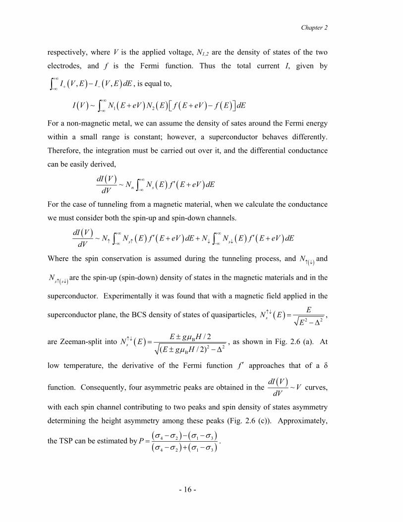
superconductor. Experimentally it was found that with a magnetic field applied in the
superconductor plane, the BCS density of states of quasiparticles, ( )2 2sEN E
E↑↓ =
− Δ,
are Zeeman-split into ( ) B2 2
B
/ 2( / 2)
sE g HN E
E g Hμ
μ↑↓ ±
=± −Δ
, as shown in Fig. 2.6 (a). At
low temperature, the derivative of the Fermi function f ′ approaches that of a δ
function. Consequently, four asymmetric peaks are obtained in the ( ) ~dI V
VdV
curves,
with each spin channel contributing to two peaks and spin density of states asymmetry
determining the height asymmetry among these peaks (Fig. 2.6 (c)). Approximately,
the TSP can be estimated by ( ) ( )( ) ( )
4 2 1 3
4 2 1 3
Pσ σ σ σσ σ σ σ
− − −=
− + −.
- 16 -
Chapter 2
Fig. 2.6 Superconducting-ferromagnetic-metal tunneling[21]. (a) BCS density of states of a superconductor as a function of voltage in a magnetic field; (b) Temperature-dependent kernels for each spin channel in the integral expression for differential conductance; (c) Theoretical normalized conductance for each spin channel (dotted and dashed curves) and the total conductance (solid line).
In the simple BCS theory, neither the orbital depairing due to the applied field nor
spin-flip scattering due to the spin-orbit coupling (SOC) is included. A more
complicated DOS calculation was completed by Maki after taking these factors into
account[49,50],
( ) ( ) ( )( )1/ 22
0sgn Re
2 1s
s
N uN E Eu
↑↓ ±
±
⎛ ⎞⎜ ⎟=⎜ ⎟−⎝ ⎠
where u and u are implicitly defined by + − ( ) ( )1/ 2 1/ 22 21 1B u uE H uu b
u u
μ ς ±±±
±
⎛ ⎞−⎜ ⎟= + +⎜ ⎟Δ − −⎝ ⎠
∓
∓
∓ ,
is the energy gap of the superconductor, Δ ( )0sN is the normal density of states, ς is
the orbital depairing parameter, and b is the spin-orbit scattering parameter[51], In
each experiment with applied field and temperature known, the conductance curve is fit
- 17 -

Chapter 2
by Maki’s theory with , Δ ς , b and TS as fitting parameters. The TSP results can be
derived with high accuracy[52]. One of our typical TSP measurements and analysis are
shown in Fig. 3.7.
P
2.3 DEVICE PREPARATION All the films grown for the research are deposited on thermally oxidized 1-inch Si
wafers. The deposition system is equipped with several dc magnetron sputtering guns, a
plasma oxidation source, and an ion beam sputter source with a five target turret and an
electron-beam evaporation source shown in Fig. 2.7. Every time after opening the
chamber and loading cleaned Si substrates, the system is usually baked for 8~10 hours
at 120 °C, and the chamber thereafter reaches a base pressure of better than 10-8 Torr.
With the capacity of 24 substrates, any gas mixture among Ar, O2 and N2, and more
than 11 targets, the system allows to explore materials intensively and to optimize
structures efficiently.
The deposition conditions vary depending on the desired materials. Metallic films
are usually deposited with an Ar atmosphere at a pressure of 3 mTorr, and oxide
barriers are normally grown by reactive sputtering in an Ar/O2 mixture with an optimal
ratio between 97/3 and 95/5. Small permanent magnets with a field about 100 Oe are
placed above the substrate to set the moments direction in magnetic layer, especially to
establish the exchange bias.
There are two ways to make the final measurable devices: one is directly patterning
the film with in situ shadow masks; the other is patterning the devices from uniformly
deposited films using optical or ebeam lithography in a clean room. (Fig. 2.7)
2.3.1 Shadow Masked Devices
The film deposition and device patterning process is fully automated by computer. By
controlling a motor inside the chamber, both the substrate platter and the mask platter
- 18 -
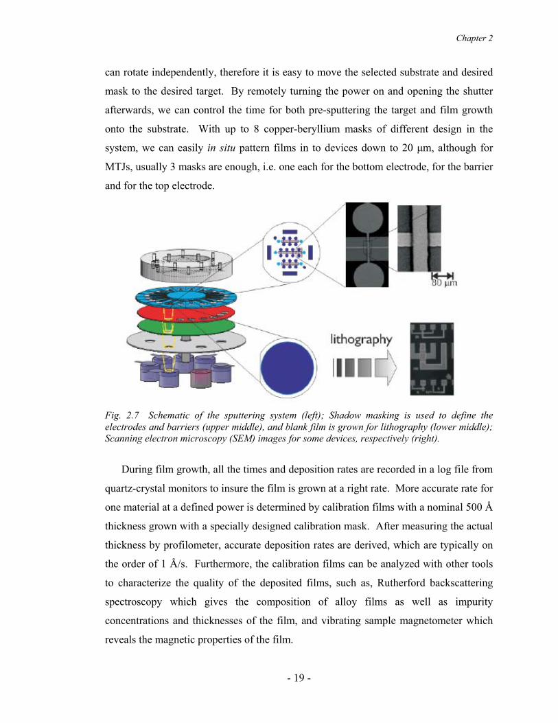
Chapter 2
can rotate independently, therefore it is easy to move the selected substrate and desired
mask to the desired target. By remotely turning the power on and opening the shutter
afterwards, we can control the time for both pre-sputtering the target and film growth
onto the substrate. With up to 8 copper-beryllium masks of different design in the
system, we can easily in situ pattern films in to devices down to 20 μm, although for
MTJs, usually 3 masks are enough, i.e. one each for the bottom electrode, for the barrier
and for the top electrode.
Fig. 2.7 Schematic of the sputtering system (left); Shadow masking is used to define the electrodes and barriers (upper middle), and blank film is grown for lithography (lower middle); Scanning electron microscopy (SEM) images for some devices, respectively (right).
During film growth, all the times and deposition rates are recorded in a log file from
quartz-crystal monitors to insure the film is grown at a right rate. More accurate rate for
one material at a defined power is determined by calibration films with a nominal 500 Å
thickness grown with a specially designed calibration mask. After measuring the actual
thickness by profilometer, accurate deposition rates are derived, which are typically on
the order of 1 Å/s. Furthermore, the calibration films can be analyzed with other tools
to characterize the quality of the deposited films, such as, Rutherford backscattering
spectroscopy which gives the composition of alloy films as well as impurity
concentrations and thicknesses of the film, and vibrating sample magnetometer which
reveals the magnetic properties of the film.
- 19 -

Chapter 2
2.3.2 Nano-Pillar Devices
Devices used for the STT studies are fabricated by ebeam lithography and standard
optical lithography. Films were grown with the same technique, however, without use
of any shadow masks. Before being brought into the clean room, samples are usually
annealed at an optimal condition, which is determined by the thermal stability and TMR
of the shadow-masked larger devices with identical multilayered structures. It takes
four major steps to fabricate the devices with a size of ~100 nm.
(i). Alignment Mark. Bilayers of photoresist (SPR670 600nm/PMGI-SFG 50nm)
are used in this step to make an undercut for ease of later liftoff. After the resists spin
and bake, they are exposed with an alignment mark mask for 1.5 seconds with 1000 W
in a contact printer. Develop the exposed resist in Optiyield developer for 45 seconds,
and deposit Ta 5 nm/Au 65 nm metal layers where thin Ta is used to increase the
adhesion. Finally, dissolve the resist with NMP and liftoff the metal, which generates
four alignment marks with size of 10×10 μm2 at each of the four corners across the
wafer.
(ii). Device Region and Bottom Electrode. Device fabrication regions with full
stack of the film are defined by ebeam lithography. After resist spinning, exposing and
developing, resist islands with bottom electrode shape remain on the wafer. Using the
resist as a hard mask, the rest of the metal layers are ion-milled to etch through the
whole film stack, thus a matrix of separated regions for later device fabrication is
formed. This process is precisely monitored by secondary ion mass spectroscopy
(SIMS). After a complete etching, Al2O3 of the same thickness as the totally etched
layers is deposited in situ by ion beam deposition (IBD). Liftoff with swabbing and
ultrasonic agitation in N-Methyl-2-Pyrrolidone (NMP), the device fabrication regions
and bottom electrodes are defined.
(iii). Tunnel Junction. Small junctions of sizes from 50×100 to 90×270 nm2 are
fabricated by ebeam lithography. Bialyers of ebeam resist (HSQ 85 nm/Duramide 40
nm) are spun onto the substrate, with each of them baked at 100 °C and 175 °C for 30
seconds. After developing, HSQ resist islands with the desired tunnel junction shape
and size remain on the wafer. Oxygen reactive ion etching treatment transfers the HSQ
- 20 -

Chapter 2
pattern onto Duramide, which also creates a slight undercut there. With HSQ/Duramide
as a hard mask, an ion-mill is used to etch through the film to the pinned ferromagnetic
layer. The ion beam starts with an incident angle between 0 to 10 degrees from
perpendicular to the surface, followed by a sidewall cleaning roughly with 2× time of
the etching. The un-etched bottom layers beneath tunneling barrier serve as bottom
electrode, and small pillars defined by the resist islands are the active tunnel junctions.
Al2O3 is then deposited with the same thickness as the etched depth. After liftoff, small
holes on top of the pillars, namely tunnel junctions, are opened for making top
electrodes.
(iv). Electrical Contact. The surface is first de-scummed with O2 plasma for 40
seconds with a pressure of 500 Torr, and then the contact metal (Ta 5 nm/Au 180 nm) is
deposited. After resist spinning, exposing, and developing, the patterns of both the top
and bottom contacts are defined. Ion-mill is used to etch away the rest of the Ta/Au
stack, and the electrical contacts are generated. Finally, resist is removed by swabbing
and ultrasonic agitation with NMP.
- 21 -

Chapter 2
REFERENCES:
[1] S. Parkin, X. Jiang, C. Kaiser, A. Panchula, K. Roche, and M. Samant,
"Magnetically Engineered Spintronic Sensors and Memory," Proc. IEEE 91, 661
(2003).
[2] M. Julliere, "Tunneling between ferromagnetic films," Phys. Lett. A 54, 225
(1975).
[3] S. Maekawa and U. Gafvert, "Electron tunneling between ferromagnetic films,"
IEEE Trans. Magn. 18, 707 (1982).
[4] J. Nowak and J. Rauluszkiewicz, "Spin dependent electron tunneling between
ferromagnetic films," J. Magn. Magn. Mater. 109, 79 (1992).
[5] T. Miyazaki and N. Tezuka, "Giant magnetic tunneling effect in Fe/Al2O3/Fe
junction," J. Magn. Magn. Mater. 139, L231 (1995).
[6] J. S. Moodera, L. R. Kinder, T. M. Wong, and R. Meservey, "Large
Magnetoresistance at Room Temperature in Ferromagnetic Thin Film Tunnel
Junctions," Phys. Rev. Lett. 74, 3273 (1995).
[7] P. LeClair, J. T. Kohlhepp, C. H. van de Vin, H. Wieldraaijer, H. J. M. Swagten,
W. J. M. de Jonge, A. H. Davis, J. M. MacLaren, J. S. Moodera, and R. Jansen,
"Band Structure and Density of States Effects in Co-Based Magnetic Tunnel
Junctions," Phys. Rev. Lett. 88, 107201 (2002).
[8] J. S. Moodera, J. Nowak, and R. J. M. van de Veerdonk, "Interface Magnetism
and Spin Wave Scattering in Ferromagnet-Insulator-Ferromagnet Tunnel
Junctions," Phys. Rev. Lett. 80, 2941 (1998).
[9] S. Yuasa, T. Nagahama, and Y. Suzuki, "Spin-Polarized Resonant Tunneling in
Magnetic Tunnel Junctions," Science 297, 234 (2002).
[10] D. Wang, C. Nordman, J. M. Daughton, Z. Qian, and J. Fink, "70% TMR at
Room Temperature for SDT Sandwich Junctions With CoFeB as Free and
Reference Layers," IEEE Trans. Magn. 40, 2269 (2004).
[11] J. J. Yang, C. Ji, Y. A. Chang, X. Ke, and M. S. Rzchowski, "Over 70%
tunneling magnetoresistance at room temperature for a CoFe and AlOx based
magnetic tunnel junction," Appl. Phys. Lett. 89, 202502 (2006).
- 22 -
Chapter 2
[12] A. M. Bratkovsky, "Tunneling of electrons in conventional and half-metallic
systems: Towards very large magnetoresistance," Phys. Rev. B 56, 2344 (1997).
[13] A. M. Bratkovsky, "Assisted tunneling in ferromagnetic junctions and half-
metallic oxides," Appl. Phys. Lett. 72, 2334 (1998).
[14] J. M. De Teresa, Barth, eacute, A. my, egrave, A. Fert, J. P. Contour, F.
Montaigne, ccedil, ois, and P. Seneor, "Role of Metal-Oxide Interface in
Determining the Spin Polarization of Magnetic Tunnel Junctions," Science 286,
507 (1999).
[15] C. T. Tanaka, J. Nowak, and J. S. Moodera, "Spin-polarized tunneling in a half-
metallic ferromagnet," J. Appl. Phys. 86, 6239 (1999).
[16] W. H. Butler, X.-G. Zhang, T. C. Schulthess, and J. M. MacLaren, "Spin-
dependent tunneling conductance of Fe|MgO|Fe sandwiches," Phys. Rev. B 63,
054416 (2001).
[17] J. Mathon and A. Umerski, "Theory of tunneling magnetoresistance of an
epitaxial Fe/MgO/Fe(001) junction," Phys. Rev. B 63, 220403 (2001).
[18] S. S. P. Parkin, C. Kaiser, A. F. Panchula, P. Rice, M. G. Samant, S.-H. Yang,
and B. Hughes, "Giant tunneling magnetoresistance at room temperature with
MgO (100) tunnel barriers," Nature Materials 3, 862 (2004).
[19] S. Yuasa, T. Nagahama, A. Fukushima, Y. Suzuki, and K. Ando, "Giant room-
temperature magnetoresistance in single-crystal Fe/MgO/Fe magnetic tunnel
junctions," Nature Materials 3, 868 (2004).
[20] S. Ikeda, J. Hayakawa, Y. Ashizawa, Y. M. Lee, K. Miura, H. Hasegawa, M.
Tsunoda, F. Matsukura, and H. Ohno, "Tunnel magnetoresistance of 604% at
300K by suppression of Ta diffusion in CoFeB/MgO/CoFeB pseudo-spin-valves
annealed at high temperature," Appl. Phys. Lett. 93, 082508 (2008).
[21] R. Meservey and P. M. Tedrow, "Spin-polarized electron tunneling," Phys. Rep.
238, 173 (1994).
[22] C. Kaiser, S. van Dijken, S.-H. Yang, H. Yang, and S. S. P. Parkin, "Role of
Tunneling Matrix Elements in Determining the Magnitude of the Tunneling
Spin Polarization of 3d Transition Metal Ferromagnetic Alloys," Phys. Rev. Lett.
94, 247203 (2005).
- 23 -
Chapter 2
[23] E. Y. Tsymbal, K. D. Belashchenko, J. P. Velev, S. S. Jaswal, M. v.
Schilfgaarde, I. I. Oleynik, and D. A. Stewart, "Interface effects in spin-
dependent tunneling," Prog. Mater. Sci. 52, 401 (2007).
[24] J. C. Slonczewski, "Conductance and exchange coupling of two ferromagnets
separated by a tunneling barrier," Phys. Rev. B 39, 6995 (1989).
[25] S. Zhang, P. M. Levy, A. C. Marley, and S. S. P. Parkin, "Quenching of
Magnetoresistance by Hot Electrons in Magnetic Tunnel Junctions," Phys. Rev.
Lett. 79, 3744 (1997).
[26] J. Klein, C. Hofener, S. Uhlenbruck, L. Alff, B. Buchner, and R. Gross, "On the
nature of grain boundaries in the colossal magnetoresistance manganites,"
Europhys. Lett. 47, 371 (1999).
[27] J. Zhang and R. M. White, "Voltage dependence of magnetoresistance in spin
dependent tunneling junctions," J. Appl. Phys. 83, 6512 (1998).
[28] L. Berger, "Emission of spin waves by a magnetic multilayer traversed by a
current," Phys. Rev. B 54 (13), 9353 (1996).
[29] J. C. Slonczewski, "Current-driven excitation of magnetic multilayers," J. Magn.
Magn. Mater. 159, L1-L7 (1996).
[30] J. A. Katine, F. J. Albert, R. A. Buhrman, E. B. Myers, and D. C. Ralph,
"Current-Driven Magnetization Reversal and Spin-Wave Excitations in
Co/Cu/Co Pillars," Phys. Rev. Lett. 84 (14), 3149-3152 (2000).
[31] E. B. Myers, D. C. Ralph, J. A. Katine, R. N. Louie, and R. A. Buhrman,
"Current-Induced Switching of Domains in Magnetic Multilayer Devices,"
Science 285, 867-870 (1999).
[32] M. Tsoi, A. G. M. Jansen, J. Bass, W.-C. Chiang, V. Tsoi, and P. Wyder,
"Generation and detection of phase-coherent current-driven magnons in
magnetic multilayers," Nature 406, 46 (2000).
[33] J. Z. Sun, "Spin-current interaction with a monodomain magnetic body: A model
study," Phys. Rev. B 62 (1), 570 (2000).
[34] J. Xiao, A. Zangwill, and M. D. Stiles, "Macrospin models of spin transfer
dynamics," Phys. Rev. B 72 (1), 014446 (2005).
- 24 -
Chapter 2
[35] J. Hayakawa, S. Ikeda, Y. M. Lee, R. SasaKi, T. Meguro, F. Matsukura, H.
Takahashi, and H. Ohno, "Current-Driven Magnetization Switching in
CoFeB/MgO/CoFeB Magnetic Tunnel Junctions," Jpn. J. Appl. Phys. 44 (41),
L1267-L1270 (2005).
[36] H. Kubota, A. Fukushima, Y. Ootani, S. Yuasa, K. Ando, H. Maehara, K.
Tsunekawa, D. D. Djayaprawira, N. Watanabe, and Y. Suzuki, "Evaluation of
Spin-Transfer Switching in CoFeB/MgO/CoFeB Magnetic Tunnel Junctions,"
Jpn. J. Appl. Phys. 44 (40), L1237-L1240 (2005).
[37] G. Bertotti, C. Serpico, I. D. Mayergoyz, A. Magni, M. d'Aquino, and R. Bonin,
"Magnetization Switching and Microwave Oscillations in Nanomagnets Driven
by Spin-Polarized Currents," Phys. Rev. Lett. 94, 127206- (2005).
[38] O. Boulle, V. Cros, J. Grollier, L. G. Pereira, C. Deranlot, F. Petroff, G. Faini, J.
Barnas, and A. Fert, "Shaped angular dependence of the spin-transfer torque and
microwave generation without magnetic field," Nat. Phys. 3, 492 (2007).
[39] A. M. Deac, A. Fukushima, H. Kubota, H. Maehara, Y. Suzuki, S. Yuasa, Y.
Nagamine, K. Tsunekawa, D. D. Djayaprawira, and N. Watanabe, "Bias-driven
high-power microwave emission from MgO-based tunnel magnetoresistance
devices," Nat. Phys. 4, 803 (2008).
[40] S. Kaka, M. R. Pufall, W. H. Rippard, T. J. Silva, S. E. Russek, and J. A. Katine,
"Mutual phase-locking of microwave spin torque nano-oscillators," Nature 437,
389 (2005).
[41] S. I. Kiselev, J. C. Sankey, I. N. Krivorotov, N. C. Emley, R. J. Schoelkopf, R.
A. Buhrman, and D. C. Ralph, "Microwave oscillations of a nanomagnet driven
by a spin-polarized current," Nature 425, 380 (2003).
[42] S. M. Rezende, F. M. de Aguiar, R. L. Rodriguez-Suarez, and A. Azevedo,
"Mode Locking of Spin Waves Excited by Direct Currents in Microwave Nano-
oscillators," Phys. Rev. Lett. 98, 087202 (2007).
[43] D. Houssameddine, U. Ebels, B. Delaet, B. Rodmacq, I. Firastrau, F. Ponthenier,
M. Brunet, C. Thirion, J. P. Michel, L. Prejbeanu-Buda, M. C. Cyrille, O. Redon,
and B. Dieny, "Spin-torque oscillator using a perpendicular polarizer and a
planar free layer," Nat. Mater. 6, 447 (2007).
- 25 -

Chapter 2
[44] A. V. Nazarov, H. M. Olson, H. Cho, K. Nikolaev, Z. Gao, S. Stokes, and B. B.
Pant, "Spin transfer stimulated microwave emission in MgO magnetic tunnel
junctions," Appl. Phys. Lett. 88, 162504 (2006).
[45] Y. S. Dedkov, U. Rudiger, and G. Guntherodt, "Evidence for the half-metallic
ferromagnetic state of Fe3O4 by spin-resolved photoelectron spectroscopy,"
Phys. Rev. B 65, 064417 (2002).
[46] R. J. Soulen, Jr., J. M. Byers, M. S. Osofsky, B. Nadgorny, T. Ambrose, S. F.
Cheng, P. R. Broussard, C. T. Tanaka, J. Nowak, J. S. Moodera, A. Barry, J. M.
Coey, nbsp, and D, "Measuring the Spin Polarization of a Metal with a
Superconducting Point Contact," Science 282, 85 (1998).
[47] C. Kaiser, A. F. Panchula, and S. S. P. Parkin, "Finite Tunneling Spin
Polarization at the Compensation Point of Rare-Earth-Metal--Transition-Metal
Alloys," Phys. Rev. Lett. 95, 047202 (2005).
[48] C. Kaiser and S. S. P. Parkin, "Spin polarization in
ferromagnet/insulator/superconductor structures with the superconductor on top
of the barrier," Appl. Phys. Lett. 84, 3582 (2004).
[49] K. Maki, "Pauli paramagnetism and superconducting state II," Prog. Theor. Phys.
32, 29 (1964).
[50] R. Meservey, P. M. Tedrow, and R. C. Bruno, "Tunneling measurements on
spin-paired superconductors with spin-orbit scattering," Phys. Rev. B 11, 4224
(1975).
[51] P. Fulde, "High field superconductivity in thin films," Adv. Phys. 22, 667 (1973).
[52] D. C. Worledge and T. H. Geballe, "Maki analysis of spin-polarized tunneling in
an oxide ferromagnet," Phys. Rev. B 62, 447 (2000).
- 26 -
Chapter 3
Chapter 3
ENHANCED TUNNELING MAGNETORESISTANCE FROM AMORPHOUS COFE ALLOY
- 27 -

Chapter 3
3.1 INTRODUCTION
As discussed in Chapter 2, the tunneling magnetoresistance (TMR) effect[1-4] in
magnetic tunnel junctions (MTJs) is of great importance both scientifically and
technologically. The MTJ not only provides an excellent platform to study the
fundamental physics of spin dependent tunneling, but also plays a central role in many
of the most useful spintronic devices including high-performance solid-state magnetic
random access memories (MRAM) and magnetic sensors[5]. It is now generally
accepted that TMR is very sensitive to the electronic structures of the electrodes and the
tunnel barrier, and to interfacial bonding between them[6,7]. Spin polarization can be
obtained from first-principle calculations, and it can be dependent on the tunneling
direction. Experiments showing the influence of crystalline anisotropy of spin
polarization on TMR have been reported[8]. A clear relationship between electrode
crystal structure and junction magnetotransport properties was also presented utilizing
Al2O3 based MTJs with Co electrodes of different crystalline phases[9]. However, in all
these work, changing the orientation of the electrodes is usually made by engineering
the buffer layers on which both the electrodes and barrier were grown. This
compromises the results of the TMR and spin polarization comparison among different
crystal structures and makes them inconclusive because TMR can also be significantly
influenced by underlayers, especially when the MTJs are annealed at elevated
temperatures.
Of particular interest technologically are amorphous ferromagnetic electrodes which
may allow for more uniform magnetic switching of devices fabricated at sub-100-nm
dimensions. Recently, ferromagnetic CoFe alloys made amorphous by the addition of
boron have become of special interest because MTJs incorporating them show the
highest TMR values at room temperature of any magnetic electrode. This is found for
MTJs formed with either amorphous Al2O3[10] or crystalline MgO tunnel barriers[3,11-
13]. Whether boron plays a direct role in increasing the TMR is however unclear.
Previous studies have also considered the effect of crystallization of CoFeB alloys via
annealing on tunneling spin polarization and TMR[14,15], but they are complicated by
the diffusion of B within the structures.
- 28 -

Chapter 3
A common method to make a normally crystalline metallic material amorphous or
glassy is by quenching it from its liquid state[16,17]. However, most simple metals will
crystallize at room temperature even at the very highest cooling rates. It is possible, in
many cases, to prevent crystallization by the incorporation of small amounts of solute
atoms which are either much smaller (e.g. B, C, Si) or much larger (e.g. Mo, Hf, Zr)
than the host elements[17]. Here it is shown that normally crystalline bcc CoFe alloys
can be made amorphous without the use of any additives and that the spin polarization
of the tunneling current and the associated TMR are correspondingly increased. The
observation of amorphous and crystalline CoFe without changing any other film-growth
conditions except its thickness provides a suitable platform to compare the TSP of one
material in two different structures. The TMR enhancement resulting from the
amorphization of a crystalline electrode emphasizes the crucial role of the electrode and
barrier interface in determining the spin dependent tunneling.
3.2 MATERIALS AND METHODS
The films were prepared using a combination of ion beam and magnetron sputtering at
ambient temperature. The structure of the thin Co70Fe30 layer was studied with high
resolution cross-section transmission electron microscopy (TEM) on multilayered films
composed of five repetitions of the sequence [44 Al2O3/tSCF SCF/100 CFB] where the
numbers are nominal thicknesses in ångström. The thin sandwiched Co70Fe30 (SCF)
layer’s thickness tSCF is 15, 20, 30, 40, and 50 Å (bottom to top), and the CFB denotes
an amorphous CoFeB layer. The repetitions are capped with 50 Ta/50 Ru and are
deposited on 100 Ta/250 Ir22Mn78/4 Co49Fe21BB30/35 Co70Fe30. Several different
compositions of the CFB layer were used. In particular, Co63Fe27B10 B (CFB10) and
Co49Fe21BB30 (CFB30) were chosen to have lower and higher crystallization
temperatures, respectively, than the maximum anneal temperature TA used in these
studies (300 °C). As can be seen clearly in Fig. 3.1(a, b) the SCF layer is amorphous
when its thickness is ≤20 Å but is crystalline when ≥30 Å. The amorphous to
crystallization transition as a function of the SCF layer thickness, which is one of the
- 29 -

Chapter 3
main points of this chapter, can also be unambiguously revealed by electron diffraction
images. These images clearly show the difference between the crystalline and
amorphous phases of the SCF layer, even though the diffraction spots in the images are
inevitably broadened by finite size effects due to the small volume used to obtain these
images (2 nm × 2 nm × thickness-of-sample (~10 nm)). Selected area electron
diffraction shows that when the SCF layer is crystalline it exhibits a bcc structure.
Electron energy loss spectroscopy (EELS)[18] was carried out using high resolution
scanning TEM to check whether B might have diffused into the SCF layer, thereby
stabilizing an amorphous state. No evidence for this was found within the spatial
resolution of the EELS (~5 Å). In any case, an added complication is that the SCF does
not wet the Al2O3 layer on which it is deposited[19,20]. Thus the SCF grows initially as
a discontinuous islanded layer, forming a continuous film only when it reaches a
thickness of ~20 Å. In cross-section, EELS will therefore see through portions of both
the SCF and CFB layers at the boundary between these layers. However, on annealing
EELS showed no change in the B profile (at 300 °C), making diffusion of B into the
SCF layer during deposition at ambient temperatures unlikely.
To check whether the morphology of the SCF layer deposited on Al2O3 plays a role
in stabilizing its amorphous structure, multilayered structures were grown in which the
SCF layers are sandwiched on either side by amorphous CFB30 layers without any
Al2O3 layers, such as, 100 Ta/250 Ir20Mn80/100 CFB30/[tCoFe=5, 10, …, and 40
SCF/100 CFB30]8/50 Ta/50 Ru. The SCF layers wet well on metals and are unlikely to
form islands, even in the thickness of just several ångstroms. TEM image (Fig. 3.2)
indicates that the SCF layers are amorphous for thicknesses up to 20 Å and crystalline
for layers above 25 Å thick, a strikingly similar dependence to that for SCF layers
deposited directly on Al2O3. This confirms that the amorphous nature of the thin SCF
layers comes from being sandwiched between two amorphous layers, not islands
formation in amorphous hosts.
- 30 -

Chapter 3
Fig. 3.1 High-resolution cross-section transmission electron microscopy images of 100 Ta/250 Ir22Mn78/4 Co49Fe21B30/35 Co70Fe30/[44 Al2O3/tSCF SCF/100 CFB]5/50 Ta/50 Ru with tSCF of 15, 20, 30, 40, and 50 Å; (a) CFB=CFB30, as deposited; (b) high magnification of a portion of (a), together with diffractograms of the four regions indicated by black square outlines in the figure. These regions are taken from (bottom to top) 20 Å SCF, 100 Å CFB30, 30 Å SCF, and 100 Å CFB30: the amorphous to crystalline transition as a function of thickness of the SCF layer is clearly revealed; (c) CFB=CFB10 annealed at 260 °C. The thicknesses (in Å) of the SCF, Al2O3, and CFB layers are labeled in green, yellow, and orange, respectively.
Interestingly, the CFB10 alloy has a much lower crystallization temperature than
CFB30 so allowing its crystallization at modest temperatures. Indeed, the TEM in Fig.
3.1(c) shows that the CFB10 has become crystalline after an anneal treatment at 260 °C.
Moreover, this induces crystallization of the SCF layers which were previously
amorphous. By contrast the CFB30 alloys remains amorphous even to 300 °C, and the
thin SCF layers remain amorphous.
- 31 -

Chapter 3
Fig. 3.2 As-deposited all-metal sample, 100 Ta/250 Ir20Mn80/100 CFB30/[tSCF=5, 10, 15, …, and 40 SCF/100 CFB30]8/50 Ta/50 Ru. The thicknesses (in Å) of the SCF, Al2O3, and CFB30 layers are labeled in green, yellow, and orange, respectively.
Thus, it is concluded that thin CoFe layers can be stabilized in an amorphous state
by sandwiching them on either side with various amorphous layers, whether insulating
or metallic, and that they display an amorphous to crystalline transition above a critical
thickness of ~25 Å. Similar results have previously been found that thin Fe films grown
on suitable substrates (eg. Y, Gd, Zr, etc.) at room temperature or below initially form
an amorphous phase up to a critical thickness of ~23 Å, and a rapid transformation to a
nanocrystalline structure throughout the total Fe layer occurs on further increasing its
thickness[21-23]. According to thermodynamic models, the amorphous-to-crystalline
transition of CoFe results from a competition between changes in the free energy of the
volume and the interfaces of the respective structures. Due to an interfacial-interaction-
induced strain relaxation, the amorphous/amorphous interface generally has a lower
- 32 -
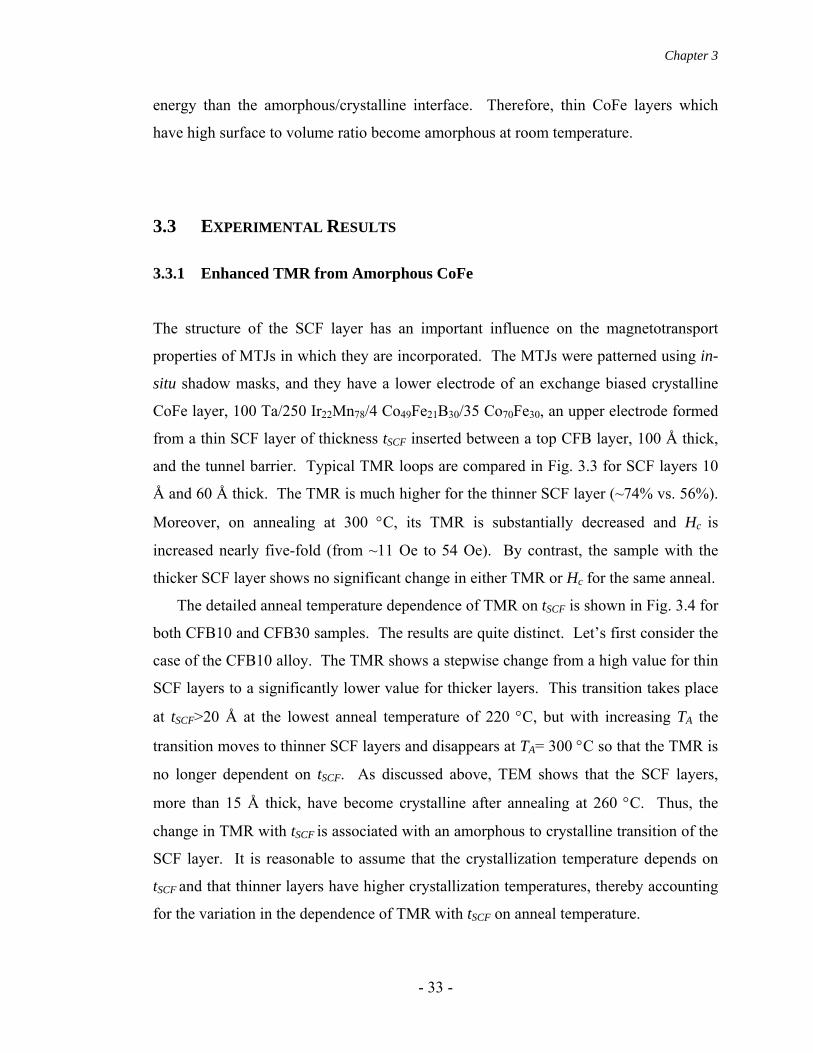
Chapter 3
energy than the amorphous/crystalline interface. Therefore, thin CoFe layers which
have high surface to volume ratio become amorphous at room temperature.
3.3 EXPERIMENTAL RESULTS
3.3.1 Enhanced TMR from Amorphous CoFe
The structure of the SCF layer has an important influence on the magnetotransport
properties of MTJs in which they are incorporated. The MTJs were patterned using in-
situ shadow masks, and they have a lower electrode of an exchange biased crystalline
CoFe layer, 100 Ta/250 Ir22Mn78/4 Co49Fe21BB30/35 Co70Fe30, an upper electrode formed
from a thin SCF layer of thickness tSCF inserted between a top CFB layer, 100 Å thick,
and the tunnel barrier. Typical TMR loops are compared in Fig. 3.3 for SCF layers 10
Å and 60 Å thick. The TMR is much higher for the thinner SCF layer (~74% vs. 56%).
Moreover, on annealing at 300 °C, its TMR is substantially decreased and Hc is
increased nearly five-fold (from ~11 Oe to 54 Oe). By contrast, the sample with the
thicker SCF layer shows no significant change in either TMR or Hc for the same anneal.
The detailed anneal temperature dependence of TMR on tSCF is shown in Fig. 3.4 for
both CFB10 and CFB30 samples. The results are quite distinct. Let’s first consider the
case of the CFB10 alloy. The TMR shows a stepwise change from a high value for thin
SCF layers to a significantly lower value for thicker layers. This transition takes place
at tSCF>20 Å at the lowest anneal temperature of 220 °C, but with increasing TA the
transition moves to thinner SCF layers and disappears at TA= 300 °C so that the TMR is
no longer dependent on tSCF. As discussed above, TEM shows that the SCF layers,
more than 15 Å thick, have become crystalline after annealing at 260 °C. Thus, the
change in TMR with tSCF is associated with an amorphous to crystalline transition of the
SCF layer. It is reasonable to assume that the crystallization temperature depends on
tSCF and that thinner layers have higher crystallization temperatures, thereby accounting
for the variation in the dependence of TMR with tSCF on anneal temperature.
- 33 -

Chapter 3
-900 -600 -300 0 3000
20
40
60
-100 0 1000
20
40
60
-100 0 1000
20
40
60
80
tSCF=60
H (Oe)
0
20
40
60
80
240°C 300°C
(b)
tSCF=10
TMR
(%)
TMR
(%)
H (Oe)TM
R (%
)
H (Oe)
Ta (100)/Ir22Mn78 (250)
Co70Fe30 (35) Co49Fe21B30 (4)
Al2O3 (24)
CFB10 or CFB30 (100) SCF (tSCF)
Ta (50)/Ru (50)
(a)
Fig. 3.3 (a) Schematic of the magnetic tunnel junction structure; (b) Major and minor (inset)
TMR loops for CFB10 samples with tSCF = 10 and 60 Å. Blue solid and red open circles denote
results after the samples are annealed at 240 °C and 300 °C, respectively.
In contrast, the dependence of TMR on tSCF for the CFB30 samples varies little with
TA (Fig. 3.4). At each anneal temperature the TMR displays a peak at tSCF~25 Å, and
then decreases to a constant value for thicker SCF layers. This is consistent with the
TEM results where the crystallinity of the SCF layer is not affected by annealing due to
the high crystallization temperature of CFB30. Note that the initial increase in TMR
with tSCF is due to the low spin polarization of the high boron content CFB30 alloy and
the initial islanded growth of the metal SCF layer on the alumina layer[24].
- 34 -

Chapter 3
50607080
220°C
50607080
240°C
50607080
TMR
(%) 260°C
50607080
280°C
0 10 20 30 40 50 60 704050607080
tSCF
(Å)
300°C
30456075
30456075
30456075
30456075
1530456075
CFB10
CFB30
Fig. 3.4 Dependence of TMR on the SCF thickness at various anneal temperatures for CFB10 (solid circle) and CFB30 (open circle) samples.
The amorphous to crystalline transition of the SCF layer is manifested as a dramatic
variation in Hc of CFB10 based MTJs, as shown in Fig. 3.5. When the SCF layer is thin
and amorphous Hc is small and independent of its thickness (see data for TA=220 °C).
However, when thin SCF layers are made crystalline by thermal annealing, Hc is
increased by almost an order of magnitude (after annealing at 300 °C) and becomes
similar to that of very thick SCF layers, which are crystalline as deposited. It is well
known that amorphous ferromagnetic materials are magnetically soft[25]. It is also well
- 35 -
Chapter 3
established that Hc of thin ferromagnetic layers increases strongly with the diameter D
of the crystalline grains (as ~D6)[26-28]. Thus, the dependence of Hc on tSCF and on TA
is readily understood from an amorphous to crystalline transition of the SCF layer and
0 10 20 30 40 50 60 700
10
20
30
40
Hc (O
e)
tSCF (Å)
CFB30
0
20
40
60
80
100
220°C 240°C 260°C 280°C 300°C
CFB10
Fig. 3.5 Dependence of Hc on the SCF thickness at various anneal temperatures for CFB10 (upper) and CFB30 (lower) samples.
CFB10 layer. When the SCF layer is thin, and amorphous as deposited, the entire free
layer crystallizes all at the same time leading to large grains whose size will be
determined by nucleation and grain growth processes within the combination of the
SCF and CFB10 layers. The underlying alumina layer will play no significant role
since it is amorphous. As the SCF layer is increased in thickness and crystallizes, the
grain size of the as-deposited SCF layer will be limited by its comparatively small
thickness (20-30 Å). (Note that the grain size of thin film layers typically varies as the
layer thickness). On annealing the CFB10 layer will crystallize but its grain size will be
templated by that of the underlying crystalline SCF layer. As tSCF is increased, its grain
size and thus the grain size of the overlying CFB10 layer on crystallization will increase
and thereby increase Hc.
- 36 -

Chapter 3
220 240 260 280 30040455055606570
20Å60Å
TM
R (%
)
TA (°C)
CFB30
505560657075
CFB10
Fig. 3.6 Dependence of TMR on anneal temperature for CFB10 (upper) and CFB30 (lower) samples with tSCF = 20 Å (red circle) and 60 Å (blue circle). The dashed lines are guides to the eye.
The dependence of Hc on tSCF for MTJs with CFB30 layers is quite similar to that
with CFB10 layers annealed at the lowest anneal temperature considered (220 °C) (Fig.
3.5). However, there is almost no change in the dependence of Hc on tSCF on annealing
up to 300 °C since the CFB30 alloy remains amorphous at these anneal temperatures.
Thus, it can be concluded that the dependence of Hc on tSCF is largely determined by the
structure and grain size of the SCF layer, and that, at these comparatively low anneal
temperatures, there is little grain growth during annealing.
An important question is whether the thickness of the SCF layer tA-C at which the
amorphous to crystalline transition takes place is correlated with the thickness tc at
which the SCF layer becomes continuous[29]. tc can be estimated from the SCF
thickness at which the TMR reaches its maximum value (assuming that tc<tA-C). Thus,
it can be estimated that tc~20-25 Å for growth of SCF on Al2O3 but only ~10-15 Å for
growth on Co40Fe40BB20 (see Section 3.3.3). Since tA-C is similar for SCF layers grown
on insulating Al2O3 and metallic CFB layers, it can be concluded that tA-C is not simply
related to tc.
- 37 -
Chapter 3
The dependence of TMR on TA is summarized in Fig. 3.6 for free layers with
representative thicknesses of 20 and 60 Å thick SCF layers for the CFB10 and CFB30
alloys, respectively. For both CFB alloys the TMR is much higher for the 20 Å
amorphous as compared to the 60 Å crystalline SCF layer. Only for the thinner CFB10
alloy is any significant variation in TMR with TA observed. In this case, the TMR
decreases on annealing to the value found for thick SCF layers, which are crystalline as
deposited.
3.3.2 Increased TSP from Amorphous CoFe
It has been discussed that when amorphous SCF layers are integrated into MTJs with
amorphous alumina tunnel barriers, significantly higher TMR is observed compared to
when these layers are crystalline. In this section, tunneling spin polarization (TSP) will
be directly compared for both amorphous and crystalline CoFe alloys using
superconducting tunneling spectroscopy (STS). It is well established that the
magnetoresistance effect in MTJs derives from spin dependent tunneling, and is largely
determined by TSP. The magnitude of TMR can be formulated in terms of the TSP for
the two corresponding ferromagnetic (FM) electrodes, P1 and P2, as
[30]. The TSP can be obtained by measuring the STS from
superconductor/insulator/FM structures[31,32]. Indeed, it is found that the TSP is
significantly enhanced for amorphous CoFe compared to its crystalline counterpart,
consistent with the previous measurements of TMR.
(1 2 1 22 / 1TMR PP PP= − )
Two sets of STS samples were deposited with the basic structure: thermally
oxidized Si substrate/45 Al95Si5/32 Al2O3/tSCF SCF /100 CFB10, or CFB30/50 Ta/50
Ru. The thickness tSCF of the SCF layer varies from 0 to 70 Å. The superconducting
layer was formed from 45-Å-thick Al95Si5, where a small amount of Si is added to
increase the Al superconducting transition temperature[31]. The STS measurements
were conducted at ~0.250 K in a magnetic field of 2 T applied in the film plane for as-
deposited samples, and after annealing the samples at a series of temperatures from 220
°C to 300 °C. The annealing was carried out in vacuum (~5×10⁻⁸ Torr) in a 1 T
- 38 -

Chapter 3
magnetic field applied along the easy axis which was set by a small in-plane magnetic
field during film deposition.
In the STS measurement, the quasi-particle density of states (DOS) in the
superconducting Al95Si5 is Zeeman-split into spin-polarized states in the presence of a
large magnetic field, thereby serving as an analyzer for the spin-polarized current. By
detailed fitting of the conductance versus voltage curves, the TSP can be extracted with
high precision[33]. Typical STS data of the tunnel junctions, 45 Al95Si5/32 Al2O3/tSCF
SCF/100 CFB10/50 Ta/50 Ru, are shown in Fig. 3.7 for tSCF = 25 and 70 Å. Four
pronounced peaks, labeled as σ1, σ2, σ3, and σ4, are observed in each curve, which
originate from contributions of the spin-up (σ1, σ3) and spin-down (σ2, σ4) states
respectively. A rough estimate of the TSP value can be derived from the following
equation[32], ( ) ( )( ) ( )
4 2 1 3
4 2 1 3
Pσ σ σ σσ σ σ σ
− − −=
− + −. Thus, from the relative magnitudes of σ1, σ2,
σ3, and σ4, it can be clearly seen that: (i) for the as-deposited samples, a 25 Å thick SCF
layer gives significantly higher TSP than that of a 70 Å thickness, i.e. the amorphous
SCF has enhanced TSP compared to the crystalline SCF; (ii) upon annealing at 300 °C,
the TSP values of both samples decrease and become similar to each other. More
accurate TSP values can be obtained by fitting the data, taking into account orbital
depairing and spin-orbit scattering in the Al95Si5 superconductor. As shown by the solid
lines in Fig. 3.7, excellent agreement with experiments is achieved using Maki’s
theory[34], The TSP of the amorphous 25 Å SCF is 55.2% whereas the TSP of the
crystalline 70 Å SCF is only 48.0%, for the as-deposited samples. By contrast, the TSP
values of the two samples become comparable after annealing at 300 °C, namely, 39.1%
and 36.2%, respectively.
The detailed dependence of TSP on tSCF at various anneal temperatures for both the
CFB10 and CFB30 samples are depicted in Fig. 3.8. For the CFB10 samples, the TSP
of the as-deposited devices shows a peak around tSCF ~25 Å, and decreases to a
significantly lower value for thicker layers. After annealing at elevated temperatures,
the position of the peak moves to thinner SCF layers, and almost disappears after the
300 °C anneal, resulting in a slight dependence of TSP on tSCF. The tSCF dependence of
- 39 -
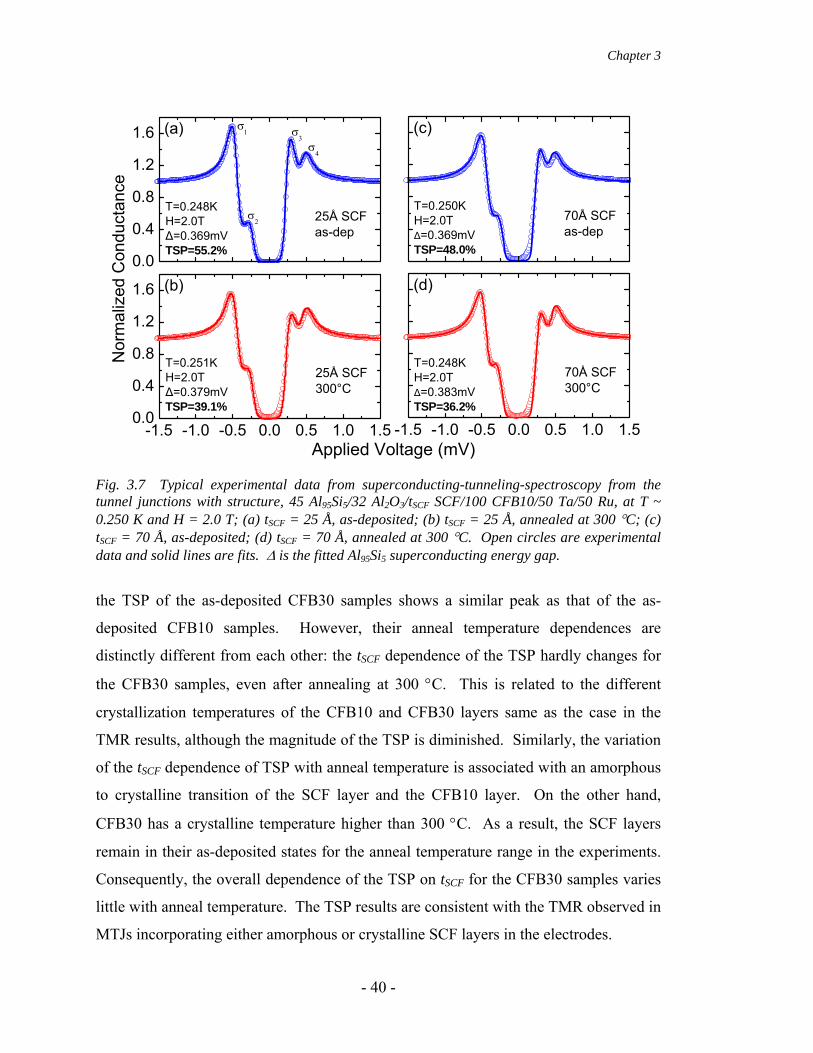
Chapter 3
-1.5 -1.0 -0.5 0.0 0.5 1.0 1.50.0
0.4
0.8
1.2
1.6
0.0
0.4
0.8
1.2
1.6N
orm
aliz
ed C
ondu
ctan
ce
T=0.251KH=2.0TΔ=0.379mVTSP=39.1%
T=0.248KH=2.0TΔ=0.369mVTSP=55.2%
σ4
σ3
σ2
(b)
(a)
σ1
25Å SCFas-dep
25Å SCF300°C
-1.5 -1.0 -0.5 0.0 0.5 1.0 1.5
T=0.250KH=2.0TΔ=0.369mVTSP=48.0%
T=0.248KH=2.0TΔ=0.383mVTSP=36.2%
(d)
(c)
70Å SCFas-dep
70Å SCF300°C
Applied Voltage (mV)
Fig. 3.7 Typical experimental data from superconducting-tunneling-spectroscopy from the tunnel junctions with structure, 45 Al95Si5/32 Al2O3/tSCF SCF/100 CFB10/50 Ta/50 Ru, at T ~ 0.250 K and H = 2.0 T; (a) tSCF = 25 Å, as-deposited; (b) tSCF = 25 Å, annealed at 300 °C; (c) tSCF = 70 Å, as-deposited; (d) tSCF = 70 Å, annealed at 300 °C. Open circles are experimental data and solid lines are fits. Δ is the fitted Al95Si5 superconducting energy gap.
the TSP of the as-deposited CFB30 samples shows a similar peak as that of the as-
deposited CFB10 samples. However, their anneal temperature dependences are
distinctly different from each other: the tSCF dependence of the TSP hardly changes for
the CFB30 samples, even after annealing at 300 °C. This is related to the different
crystallization temperatures of the CFB10 and CFB30 layers same as the case in the
TMR results, although the magnitude of the TSP is diminished. Similarly, the variation
of the tSCF dependence of TSP with anneal temperature is associated with an amorphous
to crystalline transition of the SCF layer and the CFB10 layer. On the other hand,
CFB30 has a crystalline temperature higher than 300 °C. As a result, the SCF layers
remain in their as-deposited states for the anneal temperature range in the experiments.
Consequently, the overall dependence of the TSP on tSCF for the CFB30 samples varies
little with anneal temperature. The TSP results are consistent with the TMR observed in
MTJs incorporating either amorphous or crystalline SCF layers in the electrodes.
- 40 -
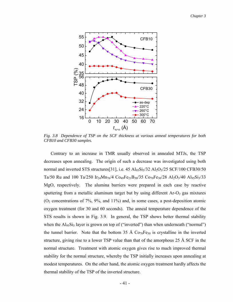
Chapter 3
0 10 20 30 40 50 60 7016
24
32
40
48
56
tSCF (Å)
TSP
(%)
CFB30
35
40
45
50
55 CFB10
as-dep 220°C 260°C 300°C
Fig. 3.8 Dependence of TSP on the SCF thickness at various anneal temperatures for both CFB10 and CFB30 samples.
Contrary to an increase in TMR usually observed in annealed MTJs, the TSP
decreases upon annealing. The origin of such a decrease was investigated using both
normal and inverted STS structures[31], i.e. 45 Al95Si5/32 Al2O3/25 SCF/100 CFB30/50
Ta/50 Ru and 100 Ta/250 Ir24Mn76/4 Co49Fe21BB30/35 Co70Fe30/28 Al2O3/40 Al95Si5/33
MgO, respectively. The alumina barriers were prepared in each case by reactive
sputtering from a metallic aluminum target but by using different Ar-O2 gas mixtures
(O2 concentrations of 7%, 9%, and 11%) and, in some cases, a post-deposition atomic
oxygen treatment (for 30 and 60 seconds). The anneal temperature dependence of the
STS results is shown in Fig. 3.9. In general, the TSP shows better thermal stability
when the Al95Si5 layer is grown on top of (“inverted”) than when underneath (“normal”)
the tunnel barrier. Note that the bottom 35 Å Co70Fe30 is crystalline in the inverted
structure, giving rise to a lower TSP value than that of the amorphous 25 Å SCF in the
normal structure. Treatment with atomic oxygen gives rise to much improved thermal
stability for the normal structure, whereby the TSP initially increases upon annealing at
modest temperatures. On the other hand, the atomic oxygen treatment hardly affects the
thermal stability of the TSP of the inverted structure.
- 41 -
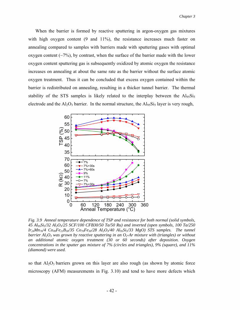
Chapter 3
When the barrier is formed by reactive sputtering in argon-oxygen gas mixtures
with high oxygen content (9 and 11%), the resistance increases much faster on
annealing compared to samples with barriers made with sputtering gases with optimal
oxygen content (~7%), by contrast, when the surface of the barrier made with the lower
oxygen content sputtering gas is subsequently oxidized by atomic oxygen the resistance
increases on annealing at about the same rate as the barrier without the surface atomic
oxygen treatment. Thus it can be concluded that excess oxygen contained within the
barrier is redistributed on annealing, resulting in a thicker tunnel barrier. The thermal
stability of the STS samples is likely related to the interplay between the Al95Si5
electrode and the Al2O3 barrier. In the normal structure, the Al95Si5 layer is very rough,
0 60 120 180 240 300 3600
10203040506070
R (k
Ω)
Anneal Temperature (°C)
354045505560
7% 7%+30s 7%+60s 9% 11% 7% 7%+30s
TSP
(%)
Fig. 3.9 Anneal temperature dependence of TSP and resistance for both normal (solid symbols, 45 Al95Si5/32 Al2O3/25 SCF/100 CFB30/50 Ta/50 Ru) and inverted (open symbols, 100 Ta/250 Ir24Mn76/4 Co49Fe21B30/35 Co70Fe30/28 Al2O3/40 Al95Si5/33 MgO) STS samples. The tunnel barrier Al2O3 was grown by reactive sputtering in an O2-Ar mixture with (triangles) or without an additional atomic oxygen treatment (30 or 60 seconds) after deposition. Oxygen concentrations in the sputter gas mixture of 7% (circles and triangles), 9% (square), and 11% (diamond) were used.
so that Al2O3 barriers grown on this layer are also rough (as shown by atomic force
microscopy (AFM) measurements in Fig. 3.10) and tend to have more defects which
- 42 -

Chapter 3
can facilitate oxygen redistribution upon annealing. During annealing the bottom
Al95Si5 will absorb oxygen from the Al2O3 barrier and form a thicker barrier, giving rise
to a pronounced increase of the sample resistance upon annealing (Fig. 3.9). The
possibility that the resistance increase could be due to the formation of boron oxide
from the diffusion of boron on annealing was ruled out by EELS measurements. No
significant boron diffusion was observed for anneal treatments up to 300 °C.
1.87 nm
0.00 nm
(a)
(b)
3.33 nm
0.00 nm
Fig. 3.10 Atomic force microscopy images (AFM) for Al2O3 barriers (a) in normal structure, 45 Al95Si5/32 Al2O3; (b) in inverted structure, 100 Ta/250 Ir22Mn78/6 Co40Fe40B20/35 Co70Fe30/32 Al2O3. Both the barriers were deposited in the optimal condition with an Ar-O2 (93/7) mixture. Clear grains with RMS ~ 0.395 nm in the normal structure and much smoother surface with RMS ~ 0.190 nm in the inverted structure were observed.
The supposed redistribution of oxygen from the barrier to the AlSi on annealing
could lead to a lack of oxygen at the Al2O3/CoFe interface and thereby account for the
observed decrease of the TSP at high annealing temperatures. Thus, adding extra
oxygen at the Al2O3/CoFe interface by a post-deposition atomic oxygen treatment
would make the TSP more thermally stable. This treatment is not possible in the
inverted structure. Rather, adding oxygen at the Al2O3/Al95Si5 interface can hardly
- 43 -
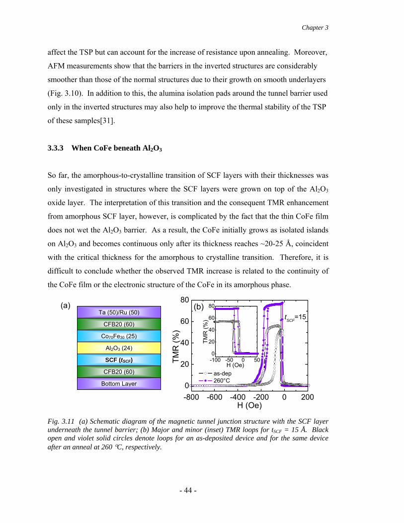
Chapter 3
affect the TSP but can account for the increase of resistance upon annealing. Moreover,
AFM measurements show that the barriers in the inverted structures are considerably
smoother than those of the normal structures due to their growth on smooth underlayers
(Fig. 3.10). In addition to this, the alumina isolation pads around the tunnel barrier used
only in the inverted structures may also help to improve the thermal stability of the TSP
of these samples[31].
3.3.3 When CoFe beneath Al2O3
So far, the amorphous-to-crystalline transition of SCF layers with their thicknesses was
only investigated in structures where the SCF layers were grown on top of the Al2O3
oxide layer. The interpretation of this transition and the consequent TMR enhancement
from amorphous SCF layer, however, is complicated by the fact that the thin CoFe film
does not wet the Al2O3 barrier. As a result, the CoFe initially grows as isolated islands
on Al2O3 and becomes continuous only after its thickness reaches ~20-25 Å, coincident
with the critical thickness for the amorphous to crystalline transition. Therefore, it is
difficult to conclude whether the observed TMR increase is related to the continuity of
the CoFe film or the electronic structure of the CoFe in its amorphous phase.
-100 -50 0 500
20
40
60
80
-800 -600 -400 -200 0 2000
20
40
60
80
H (Oe)
as-dep 260°C
(b)tSCF=15
TMR
(%)
TMR
(%)
H (Oe)
Bottom Layer
SCF (tSCF) CFB20 (60)
Al2O3 (24)
CFB20 (60) Co70Fe30 (25)
Ta (50)/Ru (50) (a)
Fig. 3.11 (a) Schematic diagram of the magnetic tunnel junction structure with the SCF layer underneath the tunnel barrier; (b) Major and minor (inset) TMR loops for tSCF = 15 Å. Black open and violet solid circles denote loops for an as-deposited device and for the same device after an anneal at 260 °C, respectively.
- 44 -

Chapter 3
In this section, it is reported that the tunneling magnetoresistance is significantly
higher when a thin amorphous CoFe layer is deposited underneath an Al2O3 tunnel
barrier. This geometry allows for the growth of continuous layers of CoFe even when
just a few ångstroms thick. Magnetotransport measurements in combination with cross-
sectional transmission electron microscopy indicate that the TMR increase is related to
the crystallinity rather than the continuity of the CoFe film.
The thin film structures were deposited with the same techniques as previous work.
The fabricated MTJs had the following structures (from bottom to top): 100 Ta/250
Ir22Mn78/4 Co49Fe21BB30/5 Co70Fe30/60 CFB20/tSCF SCF/24 Al2O3/25 Co70Fe30/60 CFB20
/50 Ta/50 Ru (Fig. 3.11), where CFB20 denotes an amorphous Co40Fe40B20B layer, and
tSCF is the thickness of the SCF layer. The TMR measurements were conducted at room
temperature. Typical resistance vs. magnetic field loops are plotted in Fig. 3.11 for the
sample with tSCF = 15 Å, both as-deposited and after an anneal at 260 °C. The anneal
significantly improves the exchange coupling between the bottom magnetic layers and
the IrMn layer, giving rise to a very high TMR of nearly 80%. The detailed SCF
thickness dependence of the TMR at various anneal temperatures is shown in Fig. 3.12.
A similar stepwise feature is clearly seen in each TMR vs. tSCF curve. The TMR values
are considerably higher when tSCF < 20-25 Å than when tSCF > 35-40 Å, with the
transition from high to low TMR values occuring at tSCF ~ 30 Å. Note that the slightly
lower TMR values at tSCF = 0 result from non-existing coverage of the SCF layer on the
bottom CFB20 layer, which has a smaller tunneling spin polarization compared to
CoFe. On the other hand, the maximum TMR value obtained at tSCF ~ 15 Å indicates
that the SCF layer becomes continuous by at least this thickness. Therefore, the
enhanced TMR for tSCF < ~ 20-25 Å cannot be explained by the continuity of the SCF
layer.
- 45 -
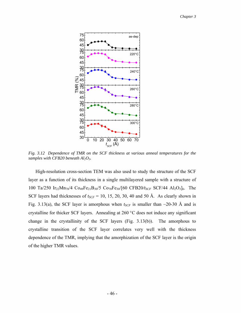
Chapter 3
30456075
as-dep
30456075
220°C
30456075
240°C
30456075
TMR
(%)
260°C
30456075
280°C
0 10 20 30 40 50 60 7030456075
tSCF (Å)
300°C
Fig. 3.12 Dependence of TMR on the SCF thickness at various anneal temperatures for the samples with CFB20 beneath Al2O3.
High-resolution cross-section TEM was also used to study the structure of the SCF
layer as a function of its thickness in a single multilayered sample with a structure of
100 Ta/250 Ir22Mn78/4 Co49Fe21BB30/5 Co70Fe30/[60 CFB20/tSCF SCF/44 Al2O3]6. The
SCF layers had thicknesses of tSCF = 10, 15, 20, 30, 40 and 50 Å. As clearly shown in
Fig. 3.13(a), the SCF layer is amorphous when tSCF is smaller than ~20-30 Å and is
crystalline for thicker SCF layers. Annealing at 260 °C does not induce any significant
change in the crystallinity of the SCF layers (Fig. 3.13(b)). The amorphous to
crystalline transition of the SCF layer correlates very well with the thickness
dependence of the TMR, implying that the amorphization of the SCF layer is the origin
of the higher TMR values.
- 46 -
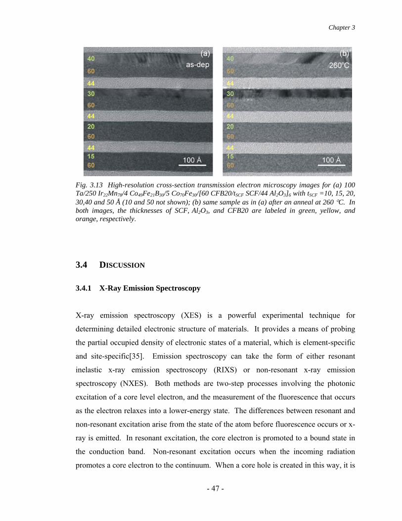
Chapter 3
Fig. 3.13 High-resolution cross-section transmission electron microscopy images for (a) 100 Ta/250 Ir22Mn78/4 Co49Fe21B30/5 Co70Fe30/[60 CFB20/tSCF SCF/44 Al2O3]6 with tSCF =10, 15, 20, 30,40 and 50 Å (10 and 50 not shown); (b) same sample as in (a) after an anneal at 260 °C. In both images, the thicknesses of SCF, Al2O3, and CFB20 are labeled in green, yellow, and orange, respectively.
3.4 DISCUSSION
3.4.1 X-Ray Emission Spectroscopy
X-ray emission spectroscopy (XES) is a powerful experimental technique for
determining detailed electronic structure of materials. It provides a means of probing
the partial occupied density of electronic states of a material, which is element-specific
and site-specific[35]. Emission spectroscopy can take the form of either resonant
inelastic x-ray emission spectroscopy (RIXS) or non-resonant x-ray emission
spectroscopy (NXES). Both methods are two-step processes involving the photonic
excitation of a core level electron, and the measurement of the fluorescence that occurs
as the electron relaxes into a lower-energy state. The differences between resonant and
non-resonant excitation arise from the state of the atom before fluorescence occurs or x-
ray is emitted. In resonant excitation, the core electron is promoted to a bound state in
the conduction band. Non-resonant excitation occurs when the incoming radiation
promotes a core electron to the continuum. When a core hole is created in this way, it is
- 47 -
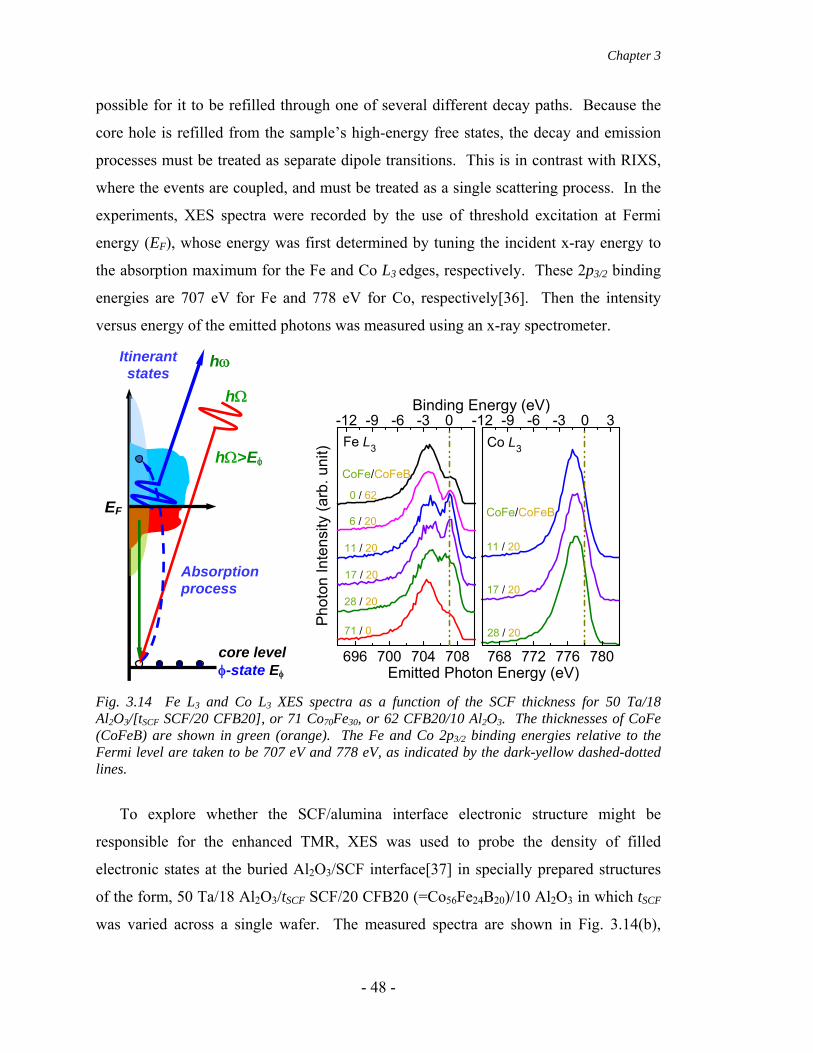
Chapter 3
possible for it to be refilled through one of several different decay paths. Because the
core hole is refilled from the sample’s high-energy free states, the decay and emission
processes must be treated as separate dipole transitions. This is in contrast with RIXS,
where the events are coupled, and must be treated as a single scattering process. In the
experiments, XES spectra were recorded by the use of threshold excitation at Fermi
energy (EF), whose energy was first determined by tuning the incident x-ray energy to
the absorption maximum for the Fe and Co L3 edges, respectively. These 2p3/2 binding
energies are 707 eV for Fe and 778 eV for Co, respectively[36]. Then the intensity
versus energy of the emitted photons was measured using an x-ray spectrometer.
696 700 704 708
-12 -9 -6 -3 0 -12 -9 -6 -3 0 3
CoFe/CoFeB
CoFe/CoFeB
Co L3
Pho
ton
Inte
nsity
(arb
. uni
t)
0 / 62
6 / 20
71 / 0
28 / 20
17 / 20
11 / 20
Emitted Photon Energy (eV)
Fe L3
768 772 776 780
28 / 20
17 / 20
11 / 20
Binding Energy (eV)
core level φ-state Eφ
Absorption process
EF
hΩ
hω
hΩ>Eφ
Itinerant states
Fig. 3.14 Fe L3 and Co L3 XES spectra as a function of the SCF thickness for 50 Ta/18 Al2O3/[tSCF SCF/20 CFB20], or 71 Co70Fe30, or 62 CFB20/10 Al2O3. The thicknesses of CoFe (CoFeB) are shown in green (orange). The Fe and Co 2p3/2 binding energies relative to the Fermi level are taken to be 707 eV and 778 eV, as indicated by the dark-yellow dashed-dotted lines.
To explore whether the SCF/alumina interface electronic structure might be
responsible for the enhanced TMR, XES was used to probe the density of filled
electronic states at the buried Al2O3/SCF interface[37] in specially prepared structures
of the form, 50 Ta/18 Al2O3/tSCF SCF/20 CFB20 (=Co56Fe24BB20)/10 Al2O3 in which tSCF
was varied across a single wafer. The measured spectra are shown in Fig. 3.14(b),
- 48 -

Chapter 3
where the valence band binding energies relative to EF are indicated. The broad,
featureless Co spectra are similar to those previously found in bulk Co and in Co/Cu
multilayers[37]. However, the Fe spectra show a feature near EF whose intensity is
significantly increased in the thickness range where the SCF is observed to be
amorphous. Moreover, since the intensity of this feature is strongest for the thinnest
SCF layers and this feature is weak in thick CFB20 layers, it can be concluded that this
feature results from modifications to the electronic structure at the Al2O3/SCF interface.
3.4.2 Band Structure Calculations
To understand whether the higher TMR of the amorphous SCF layers arises from
changes in the bulk electronic structure of this layer, density functional electronic states
were calculated for both crystalline (a bcc random solid solution) and amorphous
structures of Co70F30. These calculations reveal substantial differences in the band
structure of crystalline and glassy forms of bulk Co-Fe alloys, but a decreased spin
polarization of the electrons at the Fermi energy, inconsistent with experimental results.
In order to understand the impact of the crystallinity of the CoFe electrode on its
electronic structure and consequently its spin polarization, the density functional
electronic states of Co70F30 in two structures, bcc random solid solution and amorphous
(i.e. a glass), were calculated using the Projector Augmented Wave[38,39] method as
implemented in the Vienna Ab-initio Simulation Package (VASP)[40]. The density
functional was treated in the Generalized Gradient Approximation (GGA)[41] and all
calculations were spin polarized with collinear moments. The bcc structure was created
by random placement of 29 Fe and 67 Co atoms on bcc lattice sites (3×3×3
conventional fcc cells with large Bain strain). The atomic positions, cell volume, and
cell shape were relaxed to their local meta-stable equilibrium values using a conjugate
gradient method. The energy and forces in the relaxation process were computed with a
single k-point at Γ point. Construction of the amorphous structure began with random
packing of hard spheres with a packing ratio of 0.30. The structure was equilibrated
with VASP molecular dynamics (MD) for 2 ps at an expanded volume (about 8% larger
than equilibrium) at a temperature of 2000 K. The sample was then homogeneously
- 49 -

Chapter 3
compressed to create five samples with higher densities that were then partially
equilibrated by MD for 0.4 ps. The energies of these samples were used to determine
the equilibrium volume at 2000 K. The sample nearest the equilibrium volume was
scaled to the equilibrium volume and equilibrated for another 2 ps. Equilibration was
followed by an instantaneous quench to zero temperature. All the coordinates of the
quenched sample (cell size, cell shape, and atomic positions) were then relaxed to
values that locally minimized the energy. Similar procedures have been shown to yield
glass structures for Fe based glasses that compare well to measured partial pair
distribution functions[42,43].
-2-1012
-1.0 -0.5 0.0 0.5 1.0-10123
Fe d
-10123
Parti
al D
OS
(/at
om/e
V) Fe s
*10-2
-6 -4 -2 0 2-2-1012
Co d
Binding Energy (eV)
Co s
Fig. 3.15 Spin-resolved s- and d- partial density of states for Fe and Co in amorphous (blue and navy) and bcc crystalline (red and pink) Co70Fe30 alloy structures.
The k-point-converged densities of electronic states that were projected into angular
momentum components on atomic spheres are depicted in Fig. 3.15. Both the s- and d-
states of the CoFe alloy experience significant changes in band structure and partial
DOS when it is amorphized. The distinctive features in the energy dependence of the s-
and d- partial DOS for bcc CoFe are washed out in the amorphous state[44,45] and the
net spin polarization of the DOS at EF is slightly reduced. Therefore, the observed
TMR increase for an amorphous CoFe electrode cannot be accounted for by a larger
spin polarization of the s-electron DOS at the Fermi level, contrary to what has been
reported by Paluskar et al. for amorphous CoFeB[15].
- 50 -

Chapter 3
As an aside, it is revealed that the fluctuations in the moments of the Fe atoms from
site to site are substantially increased in the amorphous structure as compared to the
crystalline structure[45], as shown in Fig. 3.16. The Co atom moments, which vary
little in the crystalline structure, also show significant site-to-site variations in the
amorphous structure but these are smaller than those of the Fe atoms. This
demonstrates the greater sensitivity of the Fe moment to its local chemical and
structural environment.
0 10 20 30 40 50 60 70 80 90 1001.51.82.12.42.73.0
Fe in bcc Fe in amorphous Co in bcc Co in amorphous
Fe
Spi
n M
omen
t (μ B)
Atom
Co
Fig. 3.16 Spin moment of each atom in the computational ensemble for amorphous or bcc crystalline Co70Fe30. The horizontal axis indicates the label of the individual Fe and Co atoms in the calculations.
3.4.3 Explanation
Small changes in the atomic structure at the interface between a tunnel barrier and the
magnetic electrodes can give rise to significant changes in the interface density of states
and hence the spin-dependent tunneling conductance[7]. In a simple tight-binding
model, spin dependent tunneling in MTJs is largely determined by the atomic structure
and bonding at the interface, via the interplay between the on-site atomic energies and
bonding strength[7]. Amorphizing the normally crystalline CoFe alloy can introduce
significant changes in both electronic and atomic structures due to atomic relaxation.
The hopping integral with nearest-neighbors, on-site potential, and bonding strength
with oxygen can all be dramatically modified for interfacial atoms. Therefore, it may
not be surprising that the TMR and TSP values are significantly influenced by whether
the CoFe is amorphous or crystalline. Moreover, the XES strongly indicates both that
the interface electronic structure is significantly altered compared to the bulk and that
the Fe states play a dominant role. An additional peak is observed in the Fe spectrum,
- 51 -

Chapter 3
whose intensity is maximized for thicknesses at which the SCF layer is amorphous. On
the other hand, the Co partial DOS does not show a significant dependence on the SCF
thickness. The strong dependence of the partial DOS of the Fe 3d band on the thickness
of the SCF layer is consistent with the notion that Fe is more easily affected by
structural changes of the CoFe, as revealed by ab initio calculations in Fig. 3.16.
Material variations have explored in the composition of the SCF layer from pure Co to
pure Fe and it is found that the highest TMR values for amorphous SCF layers with
compositions is near Co70Fe30. It is believed that the chemical bonding at the SCF
interface with alumina is important[6]. Stronger bonding with oxygen is expected for
Fe as compared to Co at the alumina interface from bond energy considerations, and
stronger bonding with oxygen can also be expected at the interface for amorphous CoFe
since atoms are no longer restricted by the crystalline order, which helps spin dependent
tunneling and increases the tunneling spin polarization[6]. It is reasonable for us to
speculate that this difference could be accentuated when the ferromagnetic electrode is
in an amorphous compared to a crystalline state due to atomic relaxation. Therefore, it
is proposed that the enhanced TMR may rather be attributed to changes at the
SCF/Al2O3 interface upon the CoFe amorphization.
- 52 -
Chapter 3
3.5 SUMMARY
Using cross-section transmission electron microscopy it is shown that films of CoFe
alloys, sandwiched between two conventional amorphous materials, undergo an
amorphous-to-crystalline transition at a critical thickness of ~25-30 Å. When these
amorphous layers are integrated into magnetic tunnel junctions with amorphous alumina
tunnel barriers, significantly higher tunneling magnetoresistance and tunneling spin
polarization are found compared to when these layers are made crystalline, e.g. by
heating or by thickening them. Ab initio electronic structure calculations show
substantial differences in the band structure of crystalline and amorphous forms of bulk
CoFe alloys. However, the calculated spin polarization at the Fermi energy is reduced
when CoFe is amorphous, contrary to an explanation of the experimental observation in
terms of the bulk electronic states in bcc and amorphous CoFe. The calculations also
reveal the greater sensitivity of the Fe moment to its local chemical and structural
environment. Indeed, x-ray emission spectroscopy shows a significant increase in the
Fe, but not the Co, 3d density of states at the Fermi energy for thin amorphous CoFe
layers. Therefore, it is postulated that the increased tunneling magnetoresistance is
likely due to changes in interfacial bonding at the alumina/CoFe interface caused by
amorphization induced atomic relaxation.
- 53 -

Chapter 3
REFERENCES:
[1] T. Miyazaki and N. Tezuka, "Giant magnetic tunneling effect in Fe/Al2O3/Fe
junction," J. Magn. Magn. Mater. 139, L231 (1995).
[2] J. S. Moodera, L. R. Kinder, T. M. Wong, and R. Meservey, "Large
Magnetoresistance at Room Temperature in Ferromagnetic Thin Film Tunnel
Junctions," Phys. Rev. Lett. 74, 3273 (1995).
[3] S. S. P. Parkin, C. Kaiser, A. F. Panchula, P. Rice, M. G. Samant, S.-H. Yang,
and B. Hughes, "Giant tunneling magnetoresistance at room temperature with
MgO (100) tunnel barriers," Nature Materials 3, 862 (2004).
[4] E. Y. Tsymbal, O. N. Mryasov, and P. R. LeClair, "Spin-dependent tunnelling in
magnetic tunnel junctions," J. Phys. C: Condens. Matter 15, R109 (2003).
[5] S. Parkin, X. Jiang, C. Kaiser, A. Panchula, K. Roche, and M. Samant,
"Magnetically Engineered Spintronic Sensors and Memory," Proc. IEEE 91, 661
(2003).
[6] C. Kaiser, S. van Dijken, S.-H. Yang, H. Yang, and S. S. P. Parkin, "Role of
Tunneling Matrix Elements in Determining the Magnitude of the Tunneling
Spin Polarization of 3d Transition Metal Ferromagnetic Alloys," Phys. Rev. Lett.
94, 247203 (2005).
[7] E. Y. Tsymbal, K. D. Belashchenko, J. P. Velev, S. S. Jaswal, M. v.
Schilfgaarde, I. I. Oleynik, and D. A. Stewart, "Interface effects in spin-
dependent tunneling," Prog. Mater. Sci. 52, 401 (2007).
[8] S. Yuasa, E. T. T. Sato, Y. Suzuki, H. Yamamori, K. Ando, and T. Katayama,
"Magnetic tunnel junctions with single-crystal electrodes: A crystal anisotropy
of tunnel magneto-resistance," Europhys. Lett. 52, 344 (2000).
[9] P. LeClair, J. T. Kohlhepp, C. H. van de Vin, H. Wieldraaijer, H. J. M. Swagten,
W. J. M. de Jonge, A. H. Davis, J. M. MacLaren, J. S. Moodera, and R. Jansen,
"Band Structure and Density of States Effects in Co-Based Magnetic Tunnel
Junctions," Phys. Rev. Lett. 88, 107201 (2002).
- 54 -

Chapter 3
[10] D. Wang, C. Nordman, J. M. Daughton, Z. Qian, and J. Fink, "70% TMR at
Room Temperature for SDT Sandwich Junctions With CoFeB as Free and
Reference Layers," IEEE Trans. Magn. 40, 2269 (2004).
[11] D. D. Djayaprawira, K. Tsunekawa, M. Nagai, H. Maehara, S. Yamagata, N.
Watanabe, S. Yuasa, Y. Suzuki, and K. Ando, "230% room-temperature
magnetoresistance in CoFeB/MgO/CoFeB magnetic tunnel junctions," Appl.
Phys. Lett. 86, 092502 (2005).
[12] S. Ikeda, J. Hayakawa, Y. Ashizawa, Y. M. Lee, K. Miura, H. Hasegawa, M.
Tsunoda, F. Matsukura, and H. Ohno, "Tunnel magnetoresistance of 604% at
300K by suppression of Ta diffusion in CoFeB/MgO/CoFeB pseudo-spin-valves
annealed at high temperature," Appl. Phys. Lett. 93, 082508 (2008).
[13] S. Yuasa, T. Nagahama, A. Fukushima, Y. Suzuki, and K. Ando, "Giant room-
temperature magnetoresistance in single-crystal Fe/MgO/Fe magnetic tunnel
junctions," Nature Materials 3, 868 (2004).
[14] S. X. Huang, T. Y. Chen, and C. L. Chien, "Spin polarization of amorphous
CoFeB determined by point-contact Andreev reflection," Appl. Phys. Lett. 92,
242509 (2008).
[15] P. V. Paluskar, J. J. Attema, G. A. d. Wijs, S. Fiddy, E. Snoeck, J. T. Kohlhepp,
H. J. M. Swagten, R. A. d. Groot, and B. Koopmans, "Spin Tunneling in
Junctions with Disordered Ferromagnets," Phys. Rev. Lett. 100, 057205 (2008).
[16] H. A. Davies and M. R. J. Gibbs, "Amorphous Alloys," Handbook of
Magnetism and Advanced Magnetic Materials, Edited by Helmut Kronmuller
and Stuart Parkin (Willey, 2007) p. 1861.
[17] A. L. Greer, "Metallic Glasses," Science 267, 1947 (1995).
[18] EELS studies were carried out using a JEOL 2010F STEM (200 keV field
emission electron gun; energy resolution ~1.2 eV) using a high spatial resolution
(~5 Å diameter) probe and a Gatan Infina 1000 spectrometer. No evidence for B
diffusion into the SCF layer was found.
[19] C. T. Campbell, "Ultrathin metal films and particles on oxide surfaces: structural,
electronic and chemisorptive properties," Surf. Sci. Rep. 27, 1 (1997).
- 55 -

Chapter 3
[20] H. Yang, S.-H. Yang, and S. S. P. Parkin, "Crossover from Kondo-Assisted
Suppression to Co-Tunneling Enhancement of Tunneling Magnetoresistance via
Ferromagnetic Nanodots in MgO Tunnel Barriers," Nano Lett. 8, 340 (2007).
[21] S. Handschuh, J. Landes, U. Köbler, C. Sauer, G. Kisters, A. Fuss, and W. Zinn,
"Magnetic properties of amorphous Fe in Fe/Y layered structures," J. Magn.
Magn. Mat. 119, 254 (1993).
[22] U. Herr, "Metastable phases in interface controlled materials," Contemp. Phys.
41, 93 (2000).
[23] J. Landes, C. Sauer, B. Kabius, and W. Zinn, "Critical thickness of the
amorphous-nanocrystalline transition in Gd/Fe film structures," Phys. Rev. B 44,
8342 (1991).
[24] C. T. Campbell, "Ultrathin metal films and particles on oxide surfaces:
Structural, electronic and chemisorptive properties," Surf. Sci. Rep. 27 (1-3), 1-
111 (1997).
[25] G. Herzer, "Anisotropies in soft magnetic nanocrystalline alloys," J. Magn.
Magn. Mat. 294, 99 (2005).
[26] E. Kita, N. Tsukuhara, H. Sato, K. Ota, H. Yangaihara, H. Tanimoto, and N.
Ikeda, "Structure and random anisotropy in single-phase Ni nanocrystals," Appl.
Phys. Lett. 88, 152501 (2006).
[27] H. R. Liu, B. J. Qu, T. L. Ren, L. T. Liu, H. L. Xie, C. X. Li, and W. J. Ku,
"High-sensitivity GMR with low coercivity in top-IrMn spin-valves," J. Magn.
Magn. Mat. 267, 386 (2003).
[28] J. F. Loffler, H.-B. Braun, and W. Wagner, "Magnetic Correlations in
Nanostructured Ferromagnets," Phys. Rev. Lett. 85, 1990 (2000).
[29] M. Hu, S. Noda, and H. Komiyama, "Amorphous-to-crystalline transition during
the early stages of thin film growth of Cr on SiO[sub 2]," J. Appl. Phys. 93,
9336 (2003).
[30] M. Julliere, "Tunneling between ferromagnetic films," Phys. Lett. A 54, 225
(1975).
- 56 -
Chapter 3
[31] C. Kaiser and S. S. P. Parkin, "Spin polarization in
ferromagnet/insulator/superconductor structures with the superconductor on top
of the barrier," Appl. Phys. Lett. 84, 3582 (2004).
[32] R. Meservey and P. M. Tedrow, "Spin-polarized electron tunneling," Phys. Rep.
238, 173 (1994).
[33] D. J. Monsma and S. S. P. Parkin, "Spin polarization of tunneling current from
ferromagnet/Al2O3 interfaces using copper-doped aluminum superconducting
films," Appl. Phys. Lett. 77, 720 (2000).
[34] D. C. Worledge and T. H. Geballe, "Maki analysis of spin-polarized tunneling in
an oxide ferromagnet," Phys. Rev. B 62, 447 (2000).
[35] A. Kotani and S. Shin, "Resonant inelastic x-ray scattering spectra for electrons
in solids," Rev. Mod. Phys. 73, 203 (2001).
[36] J. C. Fuggle and N. Martensson, "Core-level binding energies in metals," J.
Electron Spectrosc. Relat. Phenom. 21, 275 (1980).
[37] A. Nilsson, J. Stohr, T. Wiell, M. Alden, P. Bennich, N. Wassdahl, M. G.
Samant, S. S. P. Parkin, N. Martensson, J. Nordgren, B. Johansson, and H. L.
Skriver, "Determination of the electronic density of states near buried interfaces:
Application to Co/Cu multilayers," Phys. Rev. B 54, 2917 (1996).
[38] P. E. Blochl, "Projector augmented-wave method," Phys. Rev. B 50, 17953
(1994).
[39] G. Kresse and D. Joubert, "From ultrasoft pseudopotentials to the projector
augmented-wave method," Phys. Rev. B 59, 1758 (1999).
[40] VASP is an ab initio simulation package developed at the University of Vienna
in Vienna, Austria. For details see http://cms.mpi.univie.ac.at/vasp/.
[41] J. P. Perdew and Y. Wang, "Accurate and simple analytic representation of the
electron-gas correlation energy," Phys. Rev. B 45, 13244 (1992).
[42] M. Fuentes-Cabrera, D. Nicholson, M. Widom, Y. Wang, and M. Mihalkovic,
"Ab-Initio Study of the Diffusion Coefficients in Fe-Based Liquids," Mater. Res.
Soc. Symp. Proc. 806, MM3.8 (2003).
[43] M. Mihalkovic and M. Widom, "Ab initio calculations of cohesive energies of
Fe-based glass-forming alloys," Phys. Rev. B 70, 144107 (2004).
- 57 -

Chapter 3
[44] M. Gradhand, C. Heiliger, P. Zahn, and I. Mertig, "Tunneling magnetoresistance
with amorphous electrodes," Phys. Rev. B 77, 134403 (2008).
[45] I. Turek and J. Hafner, "Magnetism of amorphous iron: From ferromagnetism to
antiferromagnetism and spin-glass behavior," Phys. Rev. B 46, 247 (1992).
- 58 -
Chapter 4
Chapter 4
TUNNELING ANISOTROPIC MAGNETORESISTANCE IN MAGNETIC TUNNEL JUNCTIONS WITH 3D TRANSITION
METALS
- 59 -
Chapter 4
4.1 INTRODUCTION
As discussed in previous chapters, magnetic tunnel junctions (MTJs) can exhibit very
large changes in resistance when the relative alignment of the electrode moments is
switched[1], and this tunneling magnetoresistance (TMR) is largely determined by the
spin polarization of the tunneling current, which is a consequence, not simply of the
spin polarized density of states (DOS) of the ferromagnetic electrodes, but also of the
tunneling matrix elements[2,3], and the spin-dependent decay of the electron
wavefunctions across the tunnel barrier[4-7]. It is also well established that the
interface between electrode and barrier plays a crucial role in the spin-dependent
tunneling process. Although using electrodes formed from the 3d transition metal (TM)
ferromagnets, such as Co-Fe alloys, and tunnel barriers formed from Al2O3 and MgO,
high TMR values of up to ~70% and ~600% are observed at room temperature[8-12],
respectively, many aspects of TMR remain poorly understood despite extensive
experimental and theoretical efforts. Of particular interest is the influence of the
detailed electronic structure of the MTJ on the bias voltage dependence of the spin-
polarized tunneling. One way to probe such an effect is to consider the angular
dependence of the tunneling resistance, or the tunneling anisotropic magnetoresistance
(TAMR) when the electrode’s moments are rotated in large magnetic fields.
On the other hand, the effect of spin-orbit coupling (SOC) on the tunneling process
was usually neglected due to the complexity that it would add to an already complicated
problem. SOC was incorporated in the calculations of TMR of
GaMnAs/GaAlAs/GaMnAs tunnel junctions by Brey et al.[13], and it was found that
the junction resistance depends on the angle between the current flow direction and the
electrode magnetization direction due to strong SOC. A large TAMR effect was
recently observed in distinctly different MTJs formed from semiconductor
heterostructures in which the ferromagnetic electrodes are formed from Mn doped
GaAs[14-16]. The obtained high TAMR effect in MTJs with only one single
ferromagnetic layer shows a rich phenomenology that could open new directions in
realizing the sensing and memory functionality. SOC plays an important role in the
Ga(Mn,As) so that the TAMR effect could be attributed to a significant anisotropy in
- 60 -

Chapter 4
the DOS linked to the magnetization direction along different crystal axes[14-16].
Although SOC is much weaker in TMs, a small TAMR effect has been predicted for
tunnel junctions with TM electrodes[17,18]. Calculations by Shick et al. predict that
the anisotropic DOS in hcp Co electrodes can lead to TAMR of ~ 0.3-1.3%[18].
Another important factor that needs to be taken into consideration is the resonant
interface states, which can produce sizeable TAMR effect due to SOC induced resonant
surface band shift via the Rashba effect when the magnetization direction changes[17].
These calculations did not, however, consider the detailed bias nor angular dependence
of the TAMR effect. In this chapter, the TAMR effect is studied in MTJs with CoFe
electrodes as the moments are rotated from in-plane to out-of-plane in sufficiently large
magnetic fields that the moments are nearly parallel to one another. A complex angular
dependence of the tunneling resistance is found with two fold and four fold components
which vary strongly with bias voltage. Distinctly different TAMR behaviors are
obtained for devices formed from highly textured crystalline MgO(001) and amorphous
Al2O3. A tight-binding model shows that a four fold angular dependence can be
explained by the presence of an interface resonant state which affects the transmission
of the contributing tunneling states through a spin-orbit interaction. In addition, the
TAMR effect from tunnel junctions with antiferromagnetic CrMo electrode will also be
briefly discussed.
4.2 EXPERIMENTS AND RESULTS
4.2.1 Samples and Measurement Setup
As introduced in Chapter 2, MTJs were fabricated on thermally oxidized Si substrates
using a combination of ion-beam and magnetron sputtering at ambient temperature. A
small in-plane magnetic field was applied during deposition to define the easy axis of
the magnetic films. In situ shadow masks were used to pattern junctions of
~ 280 80 mμ× in area. After deposition, the devices were annealed at 26 for 30
minutes in a 1T field. Two types of MTJs, with CoFe ferromagnetic electrodes and
0 C°
- 61 -

Chapter 4
either a MgO or Al2O3 tunnel barrier, were fabricated with the following structures
(from bottom to top): 100 MgO/ 50 Ta/ 250 Ir22Mn78/ 3 Co49Fe21BB30/ 60 Co70Fe30/ 34
MgO/ 25 Co70Fe30/ 150 Co49Fe21B30B / 100 Ta, and 100 TaN/ 75 Ta/ 250 Ir24Mn76/ 5
Co49Fe21BB30/ 40 Co70Fe30/ 25 Al2O3/ 20 Co70Fe30/ 100 Co49Fe21B30B / 50 Ta/ 75 Ru, where
the numbers are nominal layer thicknesses in Å.
Fig. 4.1 Schematic diagram of the TAMR measurement setup. Mixer adds the dc bias voltage and a small ac voltage together, and applies the total voltage across the tunnel junction. Lock-in amplifier is used to measure the dynamic resistance at various dc bias voltages.
Magnetotransport measurements, both dc and ac, were carried out at 10 K in a low
temperature cryostat equipped with a sample rotator and a superconducting magnet. An
ac lock-in technique was used to measure the dynamic resistance RD = dV/dI of the
tunnel junctions, with a modulation amplitude of 8 mV rms at 1001 Hz. A dc bias
voltage was simultaneously applied during the dV/dI measurement, with positive bias
corresponding to current flowing from bottom to top. The experimental geometry was
such that the magnetic field H , the normal to the film plane n , and the magnetic easy
axis were arranged in the same plane (Fig. 4.1). The field direction was fixed during the
experiment and the sample was rotated so that the field direction was rotated from in-
plane to out-of-plane. The dc and dynamic resistances were measured, using a four-
point technique, as a function of the angle θ between H and n . θ values of 0 , 18 ,
and 36 correspond to magnetic fields perpendicular to the film plane, while 90 and
correspond to fields along the in-plane easy axis direction.
° 0°
0° °
270°
- 62 -

Chapter 4
-1.0 -0.5 0.0 0.5 1.0
1.0
2.0
3.0
4.0
5.0
0.5
1.0
1.5
2.0
25
50
75
100
-0.9-0.6-0.30.0 0.3 0.6 0.9
100
200
300
400
Al2O3 MgO
MgOAl2O3dI/d
V (1
0-3Ω
−1)
TMR
(%)
V (volts)
V (volts)Fig. 4.2 The bias dependence of differential conductance for the MgO (red line) and Al2O3 (gray line) MTJs in a perpendicular field of 7 T at 10 K. The inset shows the bias dependence of the differential TMR at 10 K.
Fig. 4.2 depicts the differential conductance, dI/dV, as a function of bias voltage at
10 K in a perpendicular field of 7 T (θ = 0º), for MTJs with Al2O3 and MgO tunnel
barriers, respectively. Data at θ = 90º closely resemble those at θ = 0º. The inset in Fig.
4.2 shows the corresponding bias dependence of the differential TMR, defined as
( ) ( )( )AP
APP
dVdIdVdIdVdI −
. Here dI/dV is measured in an in-plane field; P and AP stand for
parallel and antiparallel alignment of the CoFe moments, respectively. Zero-bias TMR
values of 377% and 89% were obtained for the MTJs with MgO and Al2O3 barriers,
respectively, indicating the high quality of these devices.
4.2.2 TAMR Results
Distinct TAMR effects were observed for CoFe/MgO/CoFe and CoFe/Al2O3/CoFe
tunnel junctions; typical data at zero bias voltage are shown in Fig. 4.3, where dynamic
resistance dV/dI are normalized to their minimum values. For the MgO tunnel junction,
the resistance is larger when the field is perpendicular to the film plane than when the
field is in the film plane, giving rise to a TAMR ratio of ~ 0.3%. However, for the
Al2O3 sample, the TAMR effect is smaller than that in the MgO junction, and more
- 63 -
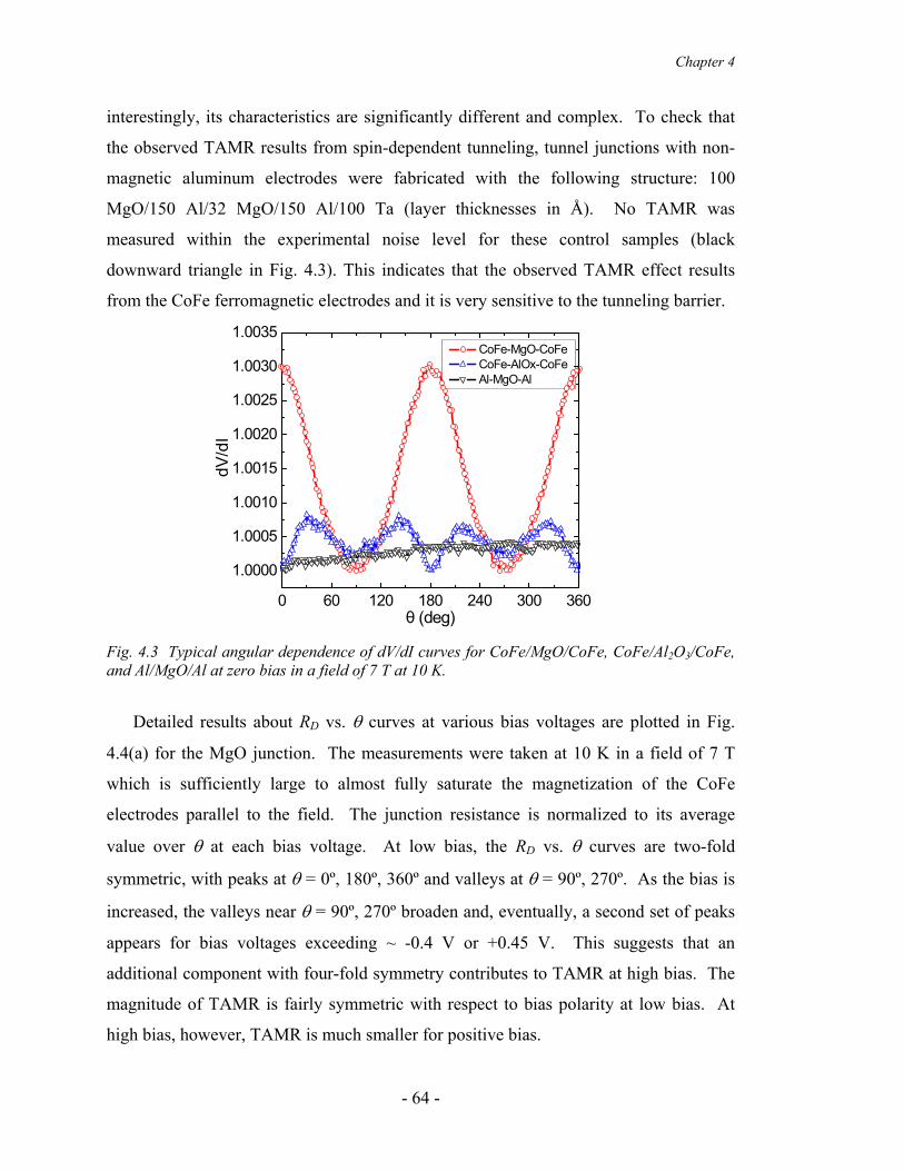
Chapter 4
interestingly, its characteristics are significantly different and complex. To check that
the observed TAMR results from spin-dependent tunneling, tunnel junctions with non-
magnetic aluminum electrodes were fabricated with the following structure: 100
MgO/150 Al/32 MgO/150 Al/100 Ta (layer thicknesses in Å). No TAMR was
measured within the experimental noise level for these control samples (black
downward triangle in Fig. 4.3). This indicates that the observed TAMR effect results
from the CoFe ferromagnetic electrodes and it is very sensitive to the tunneling barrier.
CoFe-MgO-CoFe CoFe-AlOx-CoFe Al-MgO-Al
0 60 120 180 240 300 360
1.0000
1.0005
1.0010
1.0015
1.0020
1.0025
1.0030
1.0035
dV/d
I
θ (deg) Fig. 4.3 Typical angular dependence of dV/dI curves for CoFe/MgO/CoFe, CoFe/Al2O3/CoFe, and Al/MgO/Al at zero bias in a field of 7 T at 10 K.
Detailed results about RD vs. θ curves at various bias voltages are plotted in Fig.
4.4(a) for the MgO junction. The measurements were taken at 10 K in a field of 7 T
which is sufficiently large to almost fully saturate the magnetization of the CoFe
electrodes parallel to the field. The junction resistance is normalized to its average
value over θ at each bias voltage. At low bias, the RD vs. θ curves are two-fold
symmetric, with peaks at θ = 0º, 180º, 360º and valleys at θ = 90º, 270º. As the bias is
increased, the valleys near θ = 90º, 270º broaden and, eventually, a second set of peaks
appears for bias voltages exceeding ~ -0.4 V or +0.45 V. This suggests that an
additional component with four-fold symmetry contributes to TAMR at high bias. The
magnitude of TAMR is fairly symmetric with respect to bias polarity at low bias. At
high bias, however, TAMR is much smaller for positive bias.
- 64 -
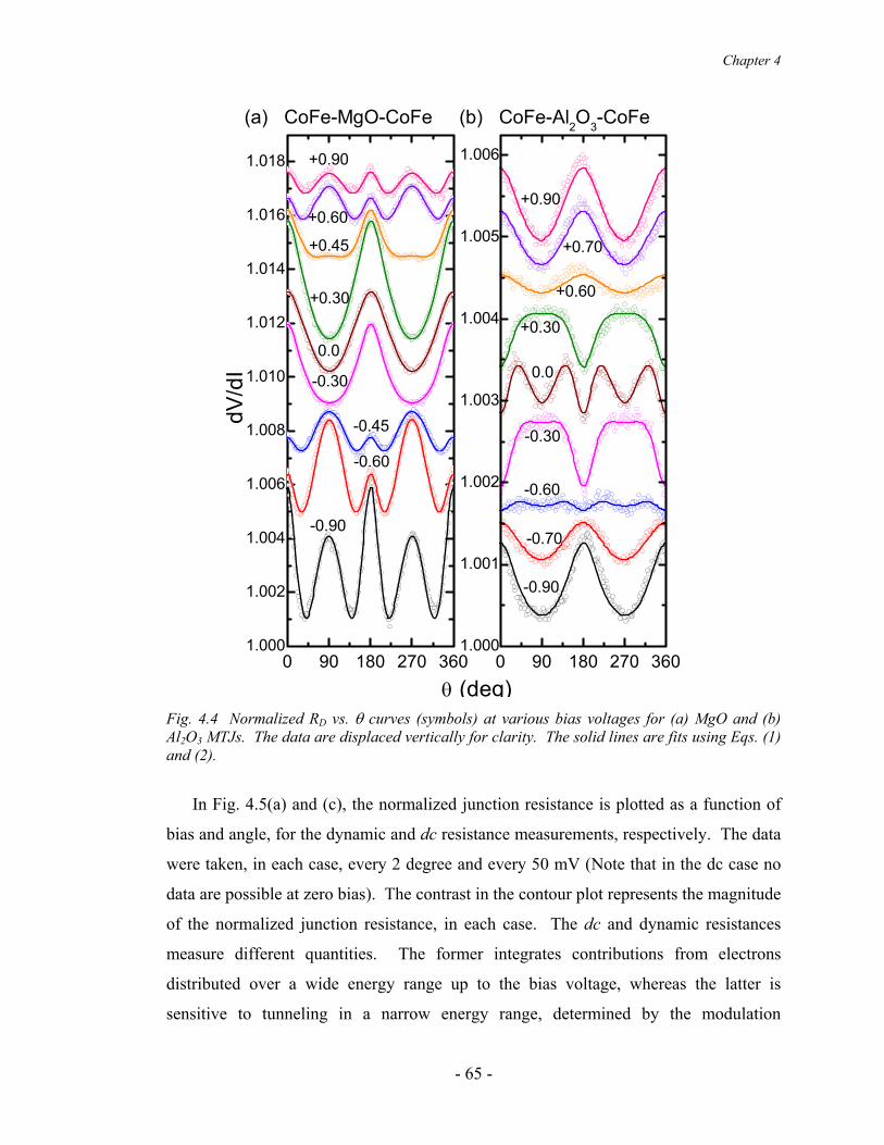
Chapter 4
0 90 180 270 3601.000
1.002
1.004
1.006
1.008
1.010
1.012
1.014
1.016
1.018 +0.90
+0.60
+0.45
+0.30
-0.30
0.0
-0.45
-0.60
-0.90
θ (deg)
dV/d
I
0 90 180 270 3601.000
1.001
1.002
1.003
1.004
1.005
1.006
(a) CoFe-MgO-CoFe (b) CoFe-Al2O3-CoFe
-0.90
-0.70
-0.60
-0.30
0.0
+0.30
+0.60
+0.70
+0.90
Fig. 4.4 Normalized RD vs. θ curves (symbols) at various bias voltages for (a) MgO and (b) Al2O3 MTJs. The data are displaced vertically for clarity. The solid lines are fits using Eqs. (1) and (2).
In Fig. 4.5(a) and (c), the normalized junction resistance is plotted as a function of
bias and angle, for the dynamic and dc resistance measurements, respectively. The data
were taken, in each case, every 2 degree and every 50 mV (Note that in the dc case no
data are possible at zero bias). The contrast in the contour plot represents the magnitude
of the normalized junction resistance, in each case. The dc and dynamic resistances
measure different quantities. The former integrates contributions from electrons
distributed over a wide energy range up to the bias voltage, whereas the latter is
sensitive to tunneling in a narrow energy range, determined by the modulation
- 65 -

Chapter 4
amplitude (here, ~24 mV, peak to peak). The ac measurement clearly accentuates the
dependence of the TAMR effect on both voltage and angle, as shown in Fig. 4.5. For
this reason, the discussion will be focused on the dynamic resistance data.
For the MgO barrier, RD shows valleys at θ = 90º, 270º at low bias, which are seen
as dark areas in Fig. 4.5(a). The emergence of a second set of peaks can be clearly
distinguished above a threshold voltage of ~ -0.4 V and +0.45 V, for negative and
positive voltages, respectively. Note that this distinctive change in the angular
dependence is obscured in the dc resistance plot. Above this threshold voltage the
angular dependence shows clear evidence for some four-fold character.
The TAMR effect of the Al2O3 junction has distinctly different characteristics
compared with that of the MgO junction, as shown in Fig. 4.4(b) and 4.5(b) and (d).
Generally speaking, the TAMR magnitude is much smaller than that of the MgO
junction. In the low bias regime, the RD vs. θ curve contains a four-fold symmetric
component with minima at θ = 0º and 90º. As the bias increases, the curve becomes
largely two-fold symmetric. Below ~ ±0.6 V, the curve has a maximum at θ = 90º and a
minimum at θ = 0º. Above ~ ±0.6 V, however, the positions for the resistance extrema
are reversed, i.e., the maximum is at θ = 0º and the minimum is at θ = 90º. These
features are clearly seen in Fig. 4.5(b). Note that the basic characteristics of the contour
plots shown in Fig. 4.5 do not change with field for the explored range from 5 to 9 T.
The RD vs.θ curve at a given bias can be fitted using the following equations:
( ) ( )
)2(sin
cos4cossincos
)1(4cos2cos 1420
θφπθ
φφ
φφθ
HMH
AAAR
s
D
−=
++= −
where φ is the angle between the CoFe magnetization direction and the film normal
direction after taking into account the demagnetization field; Mn s is the saturation
magnetization of CoFe; A0, A2, and A4 are fitting parameters. The ratios A2/A0 and
A4/A0 can be understood as half of the TAMR magnitude of the components with two-
and four-fold symmetries, respectively. Their signs are related to the positions of the
resistance extrema in the RD vs.θ curves. Assuming SMπ4 = 1.93 T, excellent
agreement between data and fits are obtained (see Fig. 4.4). A2/A0 and A4/A0 values,
- 66 -
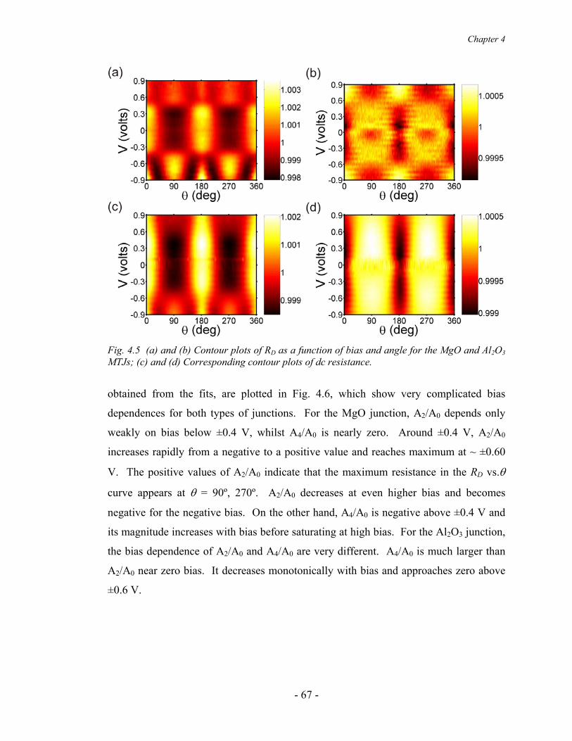
Chapter 4
Fig. 4.5 (a) and (b) Contour plots of RD as a function of bias and angle for the MgO and Al2O3 MTJs; (c) and (d) Corresponding contour plots of dc resistance.
obtained from the fits, are plotted in Fig. 4.6, which show very complicated bias
dependences for both types of junctions. For the MgO junction, A2/A0 depends only
weakly on bias below ±0.4 V, whilst A4/A0 is nearly zero. Around ±0.4 V, A2/A0
increases rapidly from a negative to a positive value and reaches maximum at ~ ±0.60
V. The positive values of A2/A0 indicate that the maximum resistance in the RD vs.θ
curve appears at θ = 90º, 270º. A2/A0 decreases at even higher bias and becomes
negative for the negative bias. On the other hand, A4/A0 is negative above ±0.4 V and
its magnitude increases with bias before saturating at high bias. For the Al2O3 junction,
the bias dependence of A2/A0 and A4/A0 are very different. A4/A0 is much larger than
A2/A0 near zero bias. It decreases monotonically with bias and approaches zero above
±0.6 V.
- 67 -

Chapter 4
-1.0 -0.5 0.0 0.5 1.0
-0.200
-0.100
0.000
0.100 CoFe-MgO-CoFe A2/A0
A4/A
0
A 2,4/A
0 (%)
-1.0 -0.5 0.0 0.5 1.0
-0.050
-0.025
0.000
0.025
0.050
CoFe-Al2O
3-CoFe
A2/A
0
A4/A0
(b)
V (volts)
(a)
Fig. 4.6 (a) and (b) Fitting parameters A2/A0 (solid circles) and A4/A0 (open squares) as a function of bias for the MgO and Al2O3 MTJs.
In contrast, A2/A0 shows a more complex bias dependence. It initially increases with
bias up to ±0.2 V. After that it shows a relatively weak bias dependence before starting
to decrease for bias exceeding ±0.5 V. A2/A0 changes sign at ~ ±0.6 V and becomes
negative at high bias. Note that in the low bias regime below ±0.4 V, A2/A0 and A4/A0
have opposite signs for the MTJs with MgO and Al2O3 barriers. This means that the
angular dependence of RD is out of phase for the two types of tunnel junctions.
4.2.3 Inelastic Electron Tunneling Spectroscopy
Inelastic electron tunneling spectroscopy (IETS) was first developed by Jacklevic and
Lambe[19]. It is a very powerful technique to study the electronic structure of chemical
compounds, as well as the detailed electronic nature of the metal/insulator interfaces
between. Spectroscopic studies of defects, impurities, magnons, and phonons have been
carried out to investigate the tunneling processes which are extremely sensitive to the
characteristics of density of states at barrier/electrode interface in a MTJ[20]. Usually,
the number of electrons tunneling inelastically is orders of magnitude smaller than those
tunneling elastically which dominate the tunneling conductance and can be well
modeled by Simmons’ equation[21]. Therefore, it is hard to find any clue about the
inelastic tunneling process in the normal I-V or conductance-V curves because the
- 68 -
Chapter 4
background from elastic tunneling is so dominating that it overwhelms any possible
spectroscopic signal from inelastic process. However, second order derivatives of the
conductance vs. voltage can often reveal peaks at which energies such inelastic
tunneling channels open.
Lock-in amplifiers were used to measure the second harmonic of the ac current (I2f)
flowing through the tunnel junctions. The amplitude (Vac) and frequency of the ac
modulation are 3-5 mV rms and 1001 Hz, respectively. Applying a dc bias voltage
superimposed with this small ac modulation signal ( )cosacV tω across a MTJ, the
flowing current can be written as,
( ) ( )
( )
( )
2
22 2
2
2 22 2
2 2
cos
1cos cos ...2
1 1cos cos 2 ...4 4
dc dc
dc dc dc
f f
dc ac
dc ac acV V
dc ac ac acV V V
I I
I V I V V t
dI d II V V t V tdV dV
dI d I d II V V t V VdV dV dV
ω
ω ω
tω ω
= +
= + + +
= + + +
Therefore, the amplitude of the first harmonics is proportional to the first-derivative
term, and the second harmonics is proportional to the second-derivative term which can
be easily detected by a lock-in amplifier. The IETS signal 2d I dV 2 , which is measured
as 22 f acI V , for the two tunnel junctions are plotted in the inset of Fig. 4.7. If the
tunneling electrons have a free-electron-like parabolic band, the IETS signal is expected
to vary linearly with bias[22]. The deviation from the parabolic band is seen by
subtracting a linear background from the IETS data, as shown in Fig. 4.7. The peak
structures at low bias around zero are due to magnon and phonon scatterings. For the
MgO junction, characteristic structures are observed around ±0.4 V and ±0.6 V,
coincident with the threshold voltages where significant changes in A2/A0 and/or A4/A0
occur. These structures might result from the electronic structure of the interface states
in the MgO tunnel junctions. For the Al2O3 MTJ, the high bias features are less
pronounced, especially at positive bias, the position of the peak moves to lower voltage.
These results clearly illustrate the electrode/barrier interface difference between the
MgO and Al2O3 tunneling junctions.
- 69 -
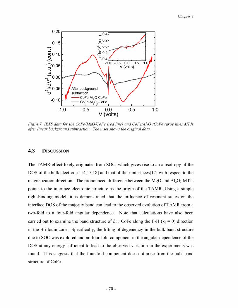
Chapter 4
-1.0 -0.5 0.0 0.5 1.0
-0.10
-0.05
0.00
0.05
0.10
0.15
0.20
d2 I/dV
2 (a.u
.) (c
orr.)
V (volts)
CoFe-MgO-CoFe CoFe-Al2O3-CoFe
After backgroundsubtraction
-1.0 -0.5 0.0 0.5 1.0-0.4
-0.2
0.0
0.2
0.4
d2 I/dV2 (a
.u.)
V (volts)
Fig. 4.7 IETS data for the CoFe/MgO/CoFe (red line) and CoFe/Al2O3/CoFe (gray line) MTJs after linear background subtraction. The inset shows the original data.
4.3 DISCUSSION
The TAMR effect likely originates from SOC, which gives rise to an anisotropy of the
DOS of the bulk electrodes[14,15,18] and that of their interfaces[17] with respect to the
magnetization direction. The pronounced difference between the MgO and Al2O3 MTJs
points to the interface electronic structure as the origin of the TAMR. Using a simple
tight-binding model, it is demonstrated that the influence of resonant states on the
interface DOS of the majority band can lead to the observed evolution of TAMR from a
two-fold to a four-fold angular dependence. Note that calculations have also been
carried out to examine the band structure of bcc CoFe along the Γ-H (k|| = 0) direction
in the Brillouin zone. Specifically, the lifting of degeneracy in the bulk band structure
due to SOC was explored and no four-fold component in the angular dependence of the
DOS at any energy sufficient to lead to the observed variation in the experiments was
found. This suggests that the four-fold component does not arise from the bulk band
structure of CoFe.
- 70 -

Chapter 4
In the calculations, the Δ1 majority-spin band in bcc CoFe[4] is modeled by a one-
dimensional tight-binding band. Consider the case when this band is coupled to a
minority resonant state localized at the interface via SOC described by the parameter λ.
The anisotropy in the conductance is determined by the anisotropy of the interface DOS
of the majority Δ1 band, which can be found from the corresponding interface Green’s
function, g(E). By solving Dyson’s equation it is found that
02 2
0
( )( ) (3)1 ( ) ( ) cosr
g Eg Eg E g Eλ φ
=−
where g0(E) is the interface Green’s function of the majority band in the absence of
SOC[3] and ( ) ( ) 10r rg E E E iγ −= − + is the Green’s function of the resonant level with
Er and γ0 being the resonance energy and width, respectively.
0 90 180 270 3600.99
1.00
1.01
1.02
1.03
1.04
-0.2
-0.407
-0.6
DO
S (a
.u.)
φ (deg)
Fig. 4.8 Angular dependence of the interface DOS of the majority band (in arbitrary units) for several energies E near the resonant energy Er = −0.4 eV. Energies are given in eV. The majority band has width 4 eV and is centered at 0.6 eV. The width of the resonant state γ0 = 10 meV, and the spin-orbit coupling parameter λ = 50 meV.
Fig. 4.8 shows the interface DOS of the majority band, ( )Im gρ π= − , as a
function of φ for several energies near the resonant level which is chosen to lie at Er =
- 71 -
Chapter 4
−0.4 eV. Away from the resonance, the angular dependence of the interface DOS has
two-fold symmetry. This two-fold angular dependence changes sign near the resonant
energy. Associated with this sign change is the onset of a significant four-fold angular
variation. Since the tunneling current will largely be determined by the interface DOS
of the majority Δ1 channel, this same variation will appear in the RD measurement when
the window of applied bias passes the resonance.
It is known that the bcc Fe(001) surface supports a minority-spin surface state[23].
The relevant interface state is present in Fe(001)/MgO/Fe tunnel junctions, as indicated
by theory and experiment[3,4,24]. A similar resonant state is likely present at the bcc
CoFe(001) surface and the CoFe(001)/MgO interface. Using a rigid band model to
estimate the change in the Fermi energy due to the increase in valence of CoFe as
compared to Fe it is found that the position of the interface resonant state for
Co70Fe30(001)/MgO interface is ~0.4 eV below the Fermi energy. This is consistent
with the observation of significant four-fold symmetry for bias beyond ~ -0.4 V or
+0.45 V for MgO based MTJs, as shown in Fig. 4.4.
Somebody might argue that electron states located at 0.4 eV below the Fermi level
cannot contribute to tunneling since the electron transmission through an energy barrier
decays exponentially with increasing barrier height. This, however, is a simple picture,
which is not in general valid. This picture is applicable only when the electron
tunneling can be described within a free-electron, single-band model. In general, the
efficiency of tunneling is controlled by evanescent states, arising from the complex
band structure of the insulator, and the energy dependence of their decay constant.[25]
For the case of Fe and other bcc ferromagnetic alloys such as the CoFe alloy used in the
experiments with MgO tunnel barriers, it has been shown (see, for example, Fig. 8 of
Butler et al.) that the electron decay constant does not vary significantly for states near
the Fermi energy, and that states at 0.4 eV and at even lower energies below the Fermi
level contribute significantly to tunneling. It is correct to point out that the tunneling in
the experiments is dominated by the CoFe majority Δ1 states for the case of CoFe/MgO.
It is proposed that these states are mixed with the known minority resonant state due to
SOC, and the tight-binding model then produces the angular variation in the DOS
shown in Fig. 4.8.
- 72 -
Chapter 4
It should be emphasized that the model assumes that the majority spin-polarized
states dominate the tunneling conductance, in particular, g(E) in Eq. (3) is the interface
Green’s function component corresponding to the majority band, not the minority
resonant states. Therefore, the experiments probe the effect of the resonance states on
the transmission of the majority Δ1 channel, not the transmission directly from the
resonant states. The latter contribution could indeed show up in the bias dependence of
the TMR although likely only for thin barriers. With increasing barrier thickness, the
contribution from resonant transmission through the minority resonant channel was
shown by Stroscio et al. to decrease quickly[23] and would not therefore be expected to
be reflected in the bias dependence of the TMR in the experiments where the barriers
are relatively thick. By contrast, the effect of the admixture of the resonant state with
the Δ1 states should be independent of the barrier thickness. Thus, it is reasonable to
conclude that the resonant state can influence the TAMR which is a small effect
(~0.5%) but not necessarily the bias voltage dependence of the TMR, which in these
samples is ~350%. The measured bias voltage dependence of TMR on the sample is
consistent with that reported by the groups of Ohno et al. and Yuasa et al. who also
report TMR values consistent with these.
Modeling of the CoFe/Al2O3 tunnel junction is not straightforward due to the
amorphous nature of the barrier. In this case, the tunneling is not dominated by one
conduction channel as in the MgO case. In addition, the electronic structure of the
CoFe/Al2O3 interface may be much more complex as compared to the CoFe/MgO
interface. For Al2O3 based MTJs a similar effect may occur due to the possibility of a
narrow majority interface resonant band derived from excess oxygen at the interface[3].
It is predicted that this band lies close to the Fermi level and is strongly transmitting.
An analysis based on a model similar to that above reveals that an interface resonant
DOS also has a significant four-fold angular variation when coupled to a bulk band via
SOC. This is consistent with the observation of a strong four-fold dependence of the
variation observed in Al2O3 at low bias in Fig. 4.4. In the case of CoFe/MgO tunnel
junction, since the transmission is dominated by the majority Δ1 states, the tight-binding
model captures the basic physics of the experimental observation; however, in the case
- 73 -

Chapter 4
of the CoFe/Al2O3 tunnel junction, one has to consider contributions from more than
one band, which is beyond the scope of the model.
4.4 OTHER RESULTS
The TAMR effect with other 3d transition metals, such as antiferromagnetic CrMo
alloy, was also investigated in MgO based tunnel junctions. Since the lattice size of this
bcc alloy is very close to that of bcc Fe, epitaxial growth of a multilayered structure
with MgO can be obtained. Samples were grown and annealed with the same
techniques as discussed before. Four sets of tunnel junctions were fabricated with the
following structures (from bottom to top): 100 MgO/50 Ta/250 Ir24Mn76/60 X/~32
MgO/100 Y/50 Ta/75 Ru, where the numbers are film thicknesses given in Ångström,
and X and Y are either Co70Fe30 or Cr85Mo15. These four types of X/MgO/Y structures
will be referred as CoFe/MgO/CoFe, CrMo/MgO/CoFe, CoFe/MgO/CrMo, and
CrMo/MgO/CrMo, for short. The measurement setup was similar to that used in the
previous section, except that only dc tunneling resistance was studied. The experiments
were also carried out at 10 K. A bias voltage was applied across the tunnel junction,
giving rise to a current flowing perpendicular to the film plane. For positive bias
voltages, the current flows from the bottom electrode to the top electrode. The
experimental geometry and the definition of the angle are the same as before, i.e., θ
values of 0 , 18 , and correspond to magnetic fields perpendicular to the film
plane, whilst
° 0° 360°
θ values of and correspond to fields parallel to the in-plane
easy axis.
90° 270°
Fig. 4.9 depicts the differential conductance dI/dV as a function of bias at 10 K in a
perpendicular field of 7 T. The dI/dV curves are reasonably symmetric for
CoFe/MgO/CoFe and CrMo/MgO/CrMo tunnel junctions. On the other hand, larger
asymmetry in dI/dV is obtained for CoFe/MgO/CrMo and CrMo/MgO/CoFe junctions.
In these junctions, the conductance is always smaller when the electrons tunnel from the
CrMo layer into the CoFe layer. This may be related to the lack of a 1Δ state near the
- 74 -

Chapter 4
Fermi level in the Cr85Mo15 electrode[26] since the decay rate of the 1Δ state is the
slowest in MgO barriers and contributes most to the tunneling conductance. The insets
of Fig. 4.9 show the I-V curves of these devices, and the high
indicators for high quality tunnel junctions.
ly nonlinear curves are the
-0.8-0.6-0.4-0.2 0.0 0.2 0.4 0.6 0.80.60.91.21.51.82.12.42.73.03.3
-0.9 -0.6 -0.3 0.0 0.3 0.6 0.9-1.5
-1.0
-0.5
0.0
0.5
1.0
1.5
I (m
A)
V (volts)
CoFe/MgO/CoFe
dI/d
V (1
0-3Ω
-1)
-0.8-0.6-0.4-0.2 0.0 0.2 0.4 0.6 0.80.0
0.5
1.0
1.5
2.0
2.5
3.0
-0.9 -0.6 -0.3 0.0 0.3 0.6 0.9
-0.6
-0.3
0.0
0.3
0.6
0.9
Voltage (V)
I (m
A)
V (volts)
CrMo/MgO/CoFe
-0.8-0.6-0.4-0.2 0.0 0.2 0.4 0.6 0.80.00.51.01.52.02.53.03.54.04.5
-0.9 -0.6 -0.3 0.0 0.3 0.6 0.9-1.6
-1.2
-0.8
-0.4
0.0
0.4
0.8
1.2
1.6
I (m
A)
V (volts)
CrMo/MgO/CrMo-0.8-0.6-0.4-0.2 0.0 0.2 0.4 0.6 0.8
0.0
0.5
1.0
1.5
2.0
2.5
3.0
-0.9 -0.6 -0.3 0.0 0.3 0.6 0.9-1.2
-0.9
-0.6
-0.3
0.0
0.3
0.6
I (m
A)
V (volts)
CoFe/MgO/CrMo
Fe, oFe/MgO/CrMo, and CrMo/MgO/CrMo tunnel junctions. The insets show the I-V curves of
the tunnel j
Fig. 4.9 Bias dependence of differential conductance for CoFe/MgO/CoFe, CrMo/MgO/CoC
unctions. The measurements were taken at 10 K in a perpendicular field of 7 T.
Distinct TAMR effects were observed at 10 K for the four types of tunnel junctions,
as shown in Fig. 4.10. In these measurements, a large (7 T) magnetic field was used to
align the moments of both electrodes along the field direction. For the
CoFe/MgO/CoFe junctions (Fig. 4.10(a)), the resistance is larger when the field is
perpendicular to the film plane than when the field is in-plane, giving rise to a TAMR
ratio of ~0.6%. As the bias increases, the valleys in the R-θ curve broadens near θ = 90º
and 270º (field in-plane). Eventually, a second set of peaks appears at large bias, same
as discussed previously. If both the CoFe electrodes are replaced by CrMo (Fig.
- 75 -

Chapter 4
4.10(d)), the basic characteristic of TAMR effect becomes reversed, i.e. maximum
peaks occur at θ = 90º and 270º now. Although smaller than that in CoFe/MgO/CoFe,
the TAMR effect in CrMo/MgO/CrMo shows fairly symmetric characteristics with
respect to bias voltage, and the R-θ curves only display twofold symmetry. In contrast
with CoFe/MgO/CoFe, no TAMR effect is discernible in CrMo/MgO/CrMo at the low
e, (b) CrMo/MgO/CoFe, (c) CoFe/MgO/CrMo, and (d) CrMo/MgO/CrMo tunnel junctions.
s an
antiferromagnetic material[27], which should be not responsive to a field of 7 T.
bias.
Fig. 4.10 Contour plots for the angular dependence of normalized dc resistance at 10 K in a field of 7 T at various bias voltages for (a) CoFe/MgO/CoF
(d). CrMo/MgO/CrMo
(b). CrMo/MgO/CoFe (a). CoFe/MgO/CoFe
(c). CoFe/MgO/CrMo
If either the bottom or top CoFe electrode is replaced by CrMo (Fig. 4.10(b) and (c)),
the bias dependence of the TAMR effect will change sign accordingly. Namely, when
electrons emerge from CoFe electrode, the TAMR effect has a peak at θ = 180º,
however, when electrons emerge from CrMo, the TAMR effect has a peak at θ = 90º.
The CrMo caused TAMR effect is somewhat unexpected since CrMo i
- 76 -

Chapter 4
0 60 120 180 240 300 360
1.000
1.001
1.002
1.003
1.004
Δ
R/R
θ (deg)
-0.90V -0.75V -0.30V +0.10V +0.30V +0.40V +0.50V +0.75V
0 60 120 180 240 300 3601.000
1.001
1.002
1.003
1.004
1.005
1.006
1.007
Δ
R/R
θ (deg)
-0.90V -0.60V -0.30V -0.10V +0.30V +0.50V +0.80V +0.90V
0 60 120 180 240 300 360
1.000
1.001
1.002
1.003
1.004
1.005
1.006
Δ
R/R
θ (deg)
-0.90V -0.30V -0.15V -0.10V -0.05V +0.05V +0.30V +0.90V
0 60 120 180 240 300 3601.000
1.001
1.002
1.003
1.004
1.005
1.006
Δ
R/R
θ (deg)
-0.90V -0.60V -0.30V -0.10V +0.30V +0.50V +0.80V +0.90V
(a) (b)
(c) (d)
Fig. 4.11 Angular dependence of normalized resistance at 10 K in a field of 7 T at various bias voltages for (a) CoFe/MgO/0 CoFe/CrMo, (b) CoFe/MgO/5 CoFe/CrMo, (c) CoFe/MgO/10 CoFe/CrMo, and (d) CoFe/MgO/15 CoFe/CrMo tunnel junctions. The curves are displaced vertically for clarity.
To make sure this sign reversal of the TAMR is not an artifact, CoFe/MgO/CrMo
tunnel junctions with a CoFe interface layer inserted between MgO and CrMo were also
fabricated and measured. It was found that an interface layer as thin as 10 Å was
sufficient to recover the bias dependence of TAMR, similar to that of CoFe/MgO/CoFe
tunnel junctions as shown in Fig. 4.11. This indicates that the observed reversal of the
TAMR effect from CrMo is very sensitive to the properties of the interface between the
barrier and the CrMo.
- 77 -

Chapter 4
The Bloch states in bcc CoFe and CrMo can have Δ1, Δ5, Δ2, or Δ2’ symmetry. In a
CoFe/MgO/CoFe tunnel junction, the Bloch state with Δ1 symmetry decays much
slower than the other states inside the MgO barrier. As a result, the tunneling
conductance is dominated by the Δ1 state. Therefore, the TAMR observed in these
tunnel junctions reflects only the anisotropy of the Δ1 state which has been fully
discussed in the previous section. The observation of a reversed TAMR effect in the
CrMo/MgO/CrMo tunnel junctions is interesting, although it is difficult to explain. For
bcc CrMo, the Bloch state with Δ1 symmetry is located at energy above the Fermi level
from the calculations with an absence of SOC. After considering the spin-orbit
interactions, bands with different symmetries mix with each other. As a result, a
marginal density of Δ1 states can exist near the Fermi level. However, the tunneling
process is still mainly dominated by other states rather than Δ1 at various bias voltages.
Therefore, in a sense, it is not so surprising that the TAMR effect is reversed in CrMo
compared to that in CoFe. Yet it is indeed surprising that the TAMR effect comes from
an antiferromagnetic material, since its antiparallel magnetic moments in the bulk film
should remain unresponsive to the applied field. To account for this effect, it might be
reasonable to assume that there exist some loose spins at the CrMo/MgO interface,
when the sample rotates in a magnetic field, these spins will change their orientation.
Due to the SOC, the spin orientation change might affect the interface density of states
contributing most to the tunneling conductance. Actually, field dependence of the
TAMR effect was also studied, and it was found that a field as small as about 1 T can
saturate the TAMR signal for each bias voltage, which means that these loose spins at
the interface are indeed very soft.
- 78 -
Chapter 4
4.5 SUMMARY
A tunneling anisotropic magnetoresistance effect has been observed in magnetic tunnel
junctions with 3d transition metal ferromagnetic electrodes for both crystalline and
amorphous tunnel barriers, despite the weak spin-orbit coupling in these systems.
Complex dependences of the junction resistance on the bias voltage and angle are
found, which are distinctly different for MgO and Al2O3 tunnel barriers. A tight-
binding model suggests that the TAMR effect derives from the anisotropy in the
interface density of states of the majority band due to mixing with a resonant state via
spin-orbit coupling. In addition, a puzzling reversed TAMR effect from CrMo has also
been observed and its mechanism requires further investigation and understanding.
- 79 -

Chapter 4
REFERENCES:
[1] S. Parkin, X. Jiang, C. Kaiser, A. Panchula, K. Roche, and M. Samant,
"Magnetically Engineered Spintronic Sensors and Memory," Proc. IEEE 91, 661
(2003).
[2] C. Kaiser, S. van Dijken, S.-H. Yang, H. Yang, and S. S. P. Parkin, "Role of
Tunneling Matrix Elements in Determining the Magnitude of the Tunneling
Spin Polarization of 3d Transition Metal Ferromagnetic Alloys," Phys. Rev.
Lett. 94, 247203 (2005).
[3] E. Y. Tsymbal, K. D. Belashchenko, J. P. Velev, S. S. Jaswal, M. v.
Schilfgaarde, I. I. Oleynik, and D. A. Stewart, "Interface effects in spin-
dependent tunneling," Prog. Mater. Sci. 52, 401 (2007).
[4] W. H. Butler, X.-G. Zhang, T. C. Schulthess, and J. M. MacLaren, "Spin-
dependent tunneling conductance of Fe|MgO|Fe sandwiches," Phys. Rev. B 63,
054416 (2001).
[5] S. S. P. Parkin, C. Kaiser, A. F. Panchula, P. Rice, M. G. Samant, S.-H. Yang,
and B. Hughes, "Giant tunneling magnetoresistance at room temperature with
MgO (100) tunnel barriers," Nature Materials 3, 862 (2004).
[6] S. Yuasa, T. Nagahama, A. Fukushima, Y. Suzuki, and K. Ando, "Giant room-
temperature magnetoresistance in single-crystal Fe/MgO/Fe magnetic tunnel
junctions," Nature Materials 3, 868 (2004).
[7] J. Mathon and A. Umerski, "Theory of tunneling magnetoresistance of an
epitaxial Fe/MgO/Fe(001) junction," Phys. Rev. B 63, 220403 (2001).
[8] T. Miyazaki and N. Tezuka, "Giant magnetic tunneling effect in Fe/Al2O3/Fe
junction," J. Magn. Magn. Mater. 139, L231 (1995).
[9] J. Hayakawa, S. Ikeda, Y. M. Lee, F. Matsukura, and H. Ohno, "Effect of high
annealing temperature on giant tunnel magnetoresistance ratio of
CoFeB/MgO/CoFeB magnetic tunnel junctions," Appl. Phys. Lett. 89, 232510
(2006).
- 80 -
Chapter 4
[10] J. J. Yang, C. Ji, Y. A. Chang, X. Ke, and M. S. Rzchowski, "Over 70%
tunneling magnetoresistance at room temperature for a CoFe and AlOx based
magnetic tunnel junction," Appl. Phys. Lett. 89, 202502 (2006).
[11] S. Ikeda, J. Hayakawa, Y. Ashizawa, Y. M. Lee, K. Miura, H. Hasegawa, M.
Tsunoda, F. Matsukura, and H. Ohno, "Tunnel magnetoresistance of 604% at
300K by suppression of Ta diffusion in CoFeB/MgO/CoFeB pseudo-spin-valves
annealed at high temperature," Appl. Phys. Lett. 93, 082508 (2008).
[12] D. Wang, C. Nordman, J. M. Daughton, Z. Qian, and J. Fink, "70% TMR at
Room Temperature for SDT Sandwich Junctions With CoFeB as Free and
Reference Layers," IEEE Trans. Magn. 40, 2269 (2004).
[13] L. Brey, C. Tejedor, and J. Fernandez-Rossier, "Tunnel magnetoresistance in
GaMnAs: Going beyond Julliere formula," Appl. Phys. Lett. 85, 1996 (2004).
[14] C. Gould, C. Ruster, T. Jungwirth, E. Girgis, G. M. Schott, R. Giraud, K.
Brunner, G. Schmidt, and L. W. Molenkamp1, "Tunneling anisotropic
magnetoresistance: A spin-valve-like tunnel magnetoresistance using a single
magnetic layer," Phys. Rev. Lett. 93, 117203 (2004).
[15] C. Ruster, C. Gould, T. Jungwirth, J. Sinova, G. M. Schott, R. Giraud, K.
Brunner, G. Schmidt, and L. W. Molenkamp, "Very Large Tunneling
Anisotropic Magnetoresistance of a (Ga,Mn)As/GaAs/(Ga,Mn)As Stack," Phys.
Rev. Lett. 94, 027203 (2005).
[16] H. Saito, S. Yuasa, and K. Ando, "Origin of the Tunnel Anisotropic
Magnetoresistance in Ga1-xMnxAs/ZnSe/Ga1-xMnxAs Magnetic Tunnel
Junctions of II-VI/III-V Heterostructures," Phys. Rev. Lett. 95, 086604 (2005).
[17] A. N. Chantis, K. D. Belashchenko, E. Y. Tsymbal, and M. van Schilfgaarde,
"Tunneling Anisotropic Magnetoresistance Driven by Resonant Surface States:
First-Principles Calculations on an Fe(001) Surface," Phys. Rev. Lett. 98,
046601 (2007).
[18] A. B. Shick, F. Maca, J. Masek, and T. Jungwirth, "Prospect for room
temperature tunneling anisotropic magnetoresistance effect: Density of states
anisotropies in CoPt systems," Phys. Rev. B 73, 024418 (2006).
- 81 -
Chapter 4
[19] R. C. Jaklevic and J. Lambe, "Molecular Vibration Spectra by Electron
Tunneling," Phys. Rev. Lett. 17, 1139 (1966).
[20] J. S. Moodera, J. Nowak, and R. J. M. van de Veerdonk, "Interface Magnetism
and Spin Wave Scattering in Ferromagnet-Insulator-Ferromagnet Tunnel
Junctions," Phys. Rev. Lett. 80, 2941 (1998).
[21] J. G. Simmons, "Generalized Formula for the Electric Tunnel Effect between
Similar Electrodes Separated by a Thin Insulating Film," J. Appl. Phys. 34, 1793
(1963).
[22] Y. Ando, T. Miyakoshi, M. Oogane, T. Miyazaki, H. Kubota, K. Ando, and S.
Yuasa, "Spin-dependent tunneling spectroscopy in single-crystal Fe/MgO/Fe
tunnel junctions," Appl. Phys. Lett. 87, 142502 (2005).
[23] J. A. Stroscio, D. T. Pierce, A. Davies, R. J. Celotta, and M. Weinert,
"Tunneling Spectroscopy of bcc (001) Surface States," Phys. Rev. Lett. 75, 2960
(1995).
[24] C. Tiusan, J. Faure-Vincent, C. Bellouard, M. Hehn, E. Jouguelet, and A.
Schuhl, "Interfacial Resonance State Probed by Spin-Polarized Tunneling in
Epitaxial Fe/MgO/Fe Tunnel Junctions," Phys. Rev. Lett. 93, 106602 (2004).
[25] P. Mavropoulos, N. Papanikolaou, and P. H. Dederichs, "Complex Band
Structure and Tunneling through Ferromagnet /Insulator /Ferromagnet
Junctions," Phys. Rev. Lett. 85, 1088 (2000).
[26] T. Nagahama, S. Yuasa, E. Tamura, and Y. Suzuki, "Spin-Dependent Tunneling
in Magnetic Tunnel Junctions with a Layered Antiferromagnetic Cr(001)
Spacer: Role of Band Structure and Interface Scattering," Phys. Rev. Lett. 95,
086602 (2005).
[27] H. Zabel, "Magnetism of chromium at surfaces, at interfaces and in thin films,"
J. Phys. C: Condens. Matter 11, 9303 (1999).
- 82 -

Chapter 5
Chapter 5
SPIN TRANSFER TORQUE INDUCED MICROWAVE EMISSION FROM MGO BASED TUNNEL JUNCTIONS
- 83 -

Chapter 5
5.1 INTRODUCTION
When a dc spin-polarized current flows through a thin ferromagnetic layer, due to the
spin-transfer torque (STT) effect, it exerts a torque on the local moments[1,2]. STT
effects were usually measured in current-perpendicular-to-plane nanopillar samples, as
discussed in Chapter 2. In magnetic sandwich structures, such as spin-valves and
magnetic tunnel junctions (MTJs), the direction of magnetization of one magnetic layer
is fixed either by exchange bias or synthetic antiferromagnetic coupling and is thus
called pinned layer (PL); however, the moments in the other electrode of thinner layer
can be manipulated via STT, thus it is usually called the free layer (FL). Experimental
observations of STT effects include static measurements of the resistance change due to
magnetization switching by the spin torque[3-5]. Under certain conditions, STT can
induce steady-state precessional excitation modes of the magnetic layer[6-11]. Most
importantly, the frequency of these modes changes with the dc current, potentially
tunable by 1 or 2 orders of magnitude (~1-100 GHz), and can be turned on and off (slew
rate) very rapidly (~1-10 ns)[12]. The precession of the free layer moment results in a
change in the resistance of the structure. Thus, this unique phenomenon opens the
possibility for the development of new classes of radio-frequency (rf) devices, such as
frequency-tunable microwave sources and filters. This effect has mostly been studied,
to date, in metallic structures. Narrow linewidths Δf have been obtained at low
temperature when the FL and PL were at a large angle to each other (Δf=10 MHz at 4.2
K)[13], or the PL consisted of a synthetic antiferromagnet (Δf=3-15 MHz at 150 K)[14].
However, both the resistance and magnetoresistance of spin-valves are small so that the
output power is very limited. Power levels of no more than ~1 nW have been observed,
which is too small for most practical applications. The recent observation of giant
tunneling magnetoresistance (TMR) in MTJs with MgO tunnel barriers[15], which have
much higher resistance and TMR than spin-valves, suggests the possibility of
correspondingly higher rf power output due to the much larger resistance change in the
tunnel junctions during the precession[16-18]. The potential achievement of both
narrow bandwidth and high power from the excitations in these MTJs highlights their
promising usefulness for controllable microwave generation.
- 84 -

Chapter 5
Here, it is demonstrated that high microwave intensity is emitted at room
temperature from MgO based MTJs which exhibit TMR values of ~100% and
resistance-area products (RA) of ~4~5 Ω×μm2. The peak amplitude and the peak
frequency have a threshold dependence on the dc bias voltage. However, it is also
found that the spectral features vary significantly from device to device. It is speculated
that these variations are due to non-uniform spatial magnetic excitation arising from
inhomogeneous current flow through the tunnel barrier.
5.2 SAMPLES AND EXPERIMENTS
The MTJs were deposited on thermally oxidized Si substrates using a combination of
ion-beam and magnetron sputtering at ambient temperature. After deposition, the films
were annealed at 300 oC for 30 minutes in a 1 T in-plane field. Using e-beam
lithography, ion milling, and optical lithography as discussed in chapter two, nanopillar
devices were patterned into various sizes from 50×100 to 90×270 nm2 always with an
aspect ratio of 1:2 or 1:3. For such small devices, it is crucial to make the tunnel barrier
both thin and of high quality, otherwise the device is so resistive that the current density
is low and STT effect is significantly reduced. Therefore, a RA of about 1 Ωμm2 is
desired. The MTJs are comprised of the following structure, 75 Ta/200 Cu/50 Ta/120
Ir22Mn78/6 Co40Fe40BB20/30 Co70Fe30/7 Ru /27 Co70Fe30/11 MgO/20 Co40Fe40B20B /50
Ta/50 Ru, where the numbers are nominal thicknesses in Ångström. The PL, i.e. the
bottom electrode below the barrier, is an exchange biased synthetic anti-ferromagnet,
and the FL is formed from 2 nm Co40Fe40BB20. Secondary ion mass spectroscopy was
used to monitor the etching process so that milling stops just before IrMn layer;
therefore, both the FL and PL are fully patterned. A bottom thin copper layer was used
to increase the conductivity. Although dozens of devices from the same wafer were
measured, the reported main results are from 80×160 nm elliptical junctions. 2
The measurement setup has four Helmholtz coils providing an in-plane field up to
1500Oe in any direction. Microwave probes with a bandwidth from dc to 40 GHz
(GGB Industries PicoProbes GS type) were used to contact the electrodes of each
- 85 -

Chapter 5
device. To reduce the microwave emission loss, several special efforts were made
during the fabrication process, such as, the bottom electrodes are isolated from each
other, the overlap capacitance between the electrodes was minimized by using a single,
very small contact finger that extended to the top of the tunnel barrier, and gold contact
pads were connected to the MTJ via planar gold contact with negligible resistance. The
characteristic impedance, Z0, of the measured transmission line was 50 Ω. A dc bias
voltage was applied through a bias tee (5550B Picosecond Pulse Labs), where positive
voltage means electrons flow from the PL to the FL which prefers the parallel state.
Reversing the voltage and current prefers the anti-parallel state. The rf emission signal
was measured using a spectrum analyzer (PSA E4448A Agilent Technologies) and an
external low-noise amplifier with a bandwidth of 100 MHz to 18GHz. The microwave
emission power will be defined by the voltage spectral density in units of /nV Hz .
Top
Bottom
G
S
Ground
Spectrum Analyzer
Amplifier
dc MTJ
Electrodes Overlap
Fig. 5.1 Schematic illustration of the measurement setup for the detection of spin transfer torque induced microware emission.
To approximate the actual microwave emission generated in the MTJs from the
detected spectrum in a spectrum analyzer, three issues should be of particular attention.
First is the signal loss in the longest transmission line used in the setup, which connects
the probes to the bias tee. Using a network analyzer, the transmission coefficient, S21,
can be measured up to 40 GHz and is shown in Fig 5.2. Below about 10 GHz, the loss
is up to 6-7 dB. Second is the subtraction of environmental noise sources. The
subtraction was done by subtracting the noise spectral powers at zero bias from the
measured spectrum at each bias voltage. With all the other experimental conditions
same, a noise spectrum is measured and recorded at zero bias, and then the desired bias
- 86 -

Chapter 5
voltage is applied and another spectrum is measured. Afterwards, the first spectrum is
subtracted from the second one, and the result is saved as the spectrum under such
experimental conditions. This procedure also removes thermal Johnson noise and the
noise from the amplifier. After considering these two factors, the remaining issue is
how much microwave emission enters the probes from the MTJs.
0 5 10 15 20 25 30 35 40-25
-20
-15
-10
-5
0S
21 (d
B)
Frequency (GHz)
Transmission Coefficient
Fig. 5.2 Transmission coefficient of microwave signals at various frequencies in the transmission line used in the setup.
G
S Amp.
Spectrum Analyzer
Fig. 5.3 Circuit model of the measurement setup for the detection of spin transfer torque induced microware emission, where Rsub is the resistance of Si substrate underneath the electrodes, Cpad is the capacitance between electrode and Si substrate, RMTJ is the resistance of MTJ, Coverlap is the overlap capacitance between top contact and bottom contact which is minimized by an extended finger.
Due to the impedance mismatch between the probe and the MTJ, it is inevitable that
some of the STT induced microwave emission is lost in coupling to the probes. The
reduced factor for the input to the probes is mainly determined by the MTJ’s resistance
and the overlap capacitance of the top and bottom contacts. The circuitry of the
measurement setup can be modeled as in Fig. 5.3. Since Rsub is very large and the CMTJ
is very small due to the tiny size of the nanopillar, they can thus be neglected for
CoverlapRMTJ CMTJ
Cpad
Cpad
Rsub
- 87 -
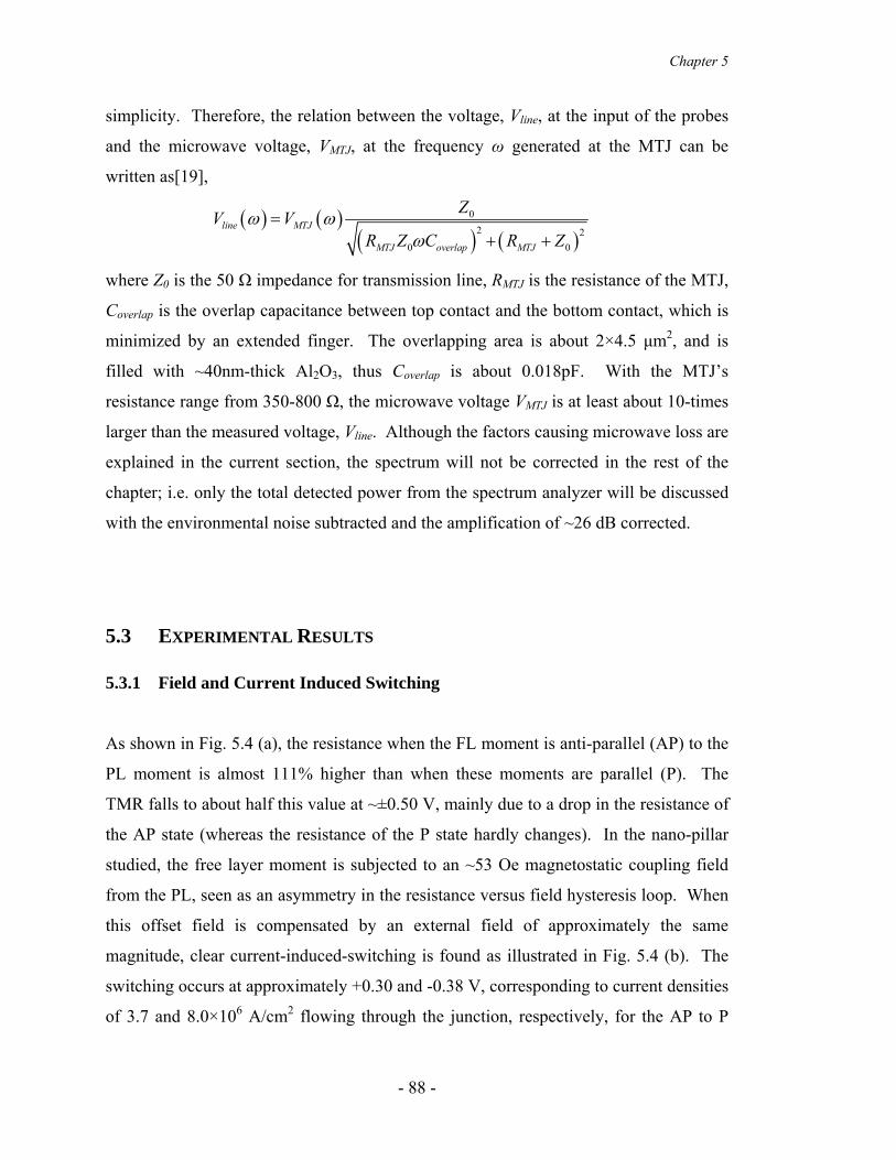
Chapter 5
simplicity. Therefore, the relation between the voltage, Vline, at the input of the probes
and the microwave voltage, VMTJ, at the frequency ω generated at the MTJ can be
written as[19],
( ) ( )( ) ( )
02 2
0 0
line MTJ
MTJ overlap MTJ
ZV VR Z C R Z
ω ωω
=+ +
where Z0 is the 50 Ω impedance for transmission line, RMTJ is the resistance of the MTJ,
Coverlap is the overlap capacitance between top contact and the bottom contact, which is
minimized by an extended finger. The overlapping area is about 2×4.5 μm2, and is
filled with ~40nm-thick Al2O3, thus Coverlap is about 0.018pF. With the MTJ’s
resistance range from 350-800 Ω, the microwave voltage VMTJ is at least about 10-times
larger than the measured voltage, Vline. Although the factors causing microwave loss are
explained in the current section, the spectrum will not be corrected in the rest of the
chapter; i.e. only the total detected power from the spectrum analyzer will be discussed
with the environmental noise subtracted and the amplification of ~26 dB corrected.
5.3 EXPERIMENTAL RESULTS
5.3.1 Field and Current Induced Switching
As shown in Fig. 5.4 (a), the resistance when the FL moment is anti-parallel (AP) to the
PL moment is almost 111% higher than when these moments are parallel (P). The
TMR falls to about half this value at ~±0.50 V, mainly due to a drop in the resistance of
the AP state (whereas the resistance of the P state hardly changes). In the nano-pillar
studied, the free layer moment is subjected to an ~53 Oe magnetostatic coupling field
from the PL, seen as an asymmetry in the resistance versus field hysteresis loop. When
this offset field is compensated by an external field of approximately the same
magnitude, clear current-induced-switching is found as illustrated in Fig. 5.4 (b). The
switching occurs at approximately +0.30 and -0.38 V, corresponding to current densities
of 3.7 and 8.0×10⁶ A/cm2 flowing through the junction, respectively, for the AP to P
- 88 -
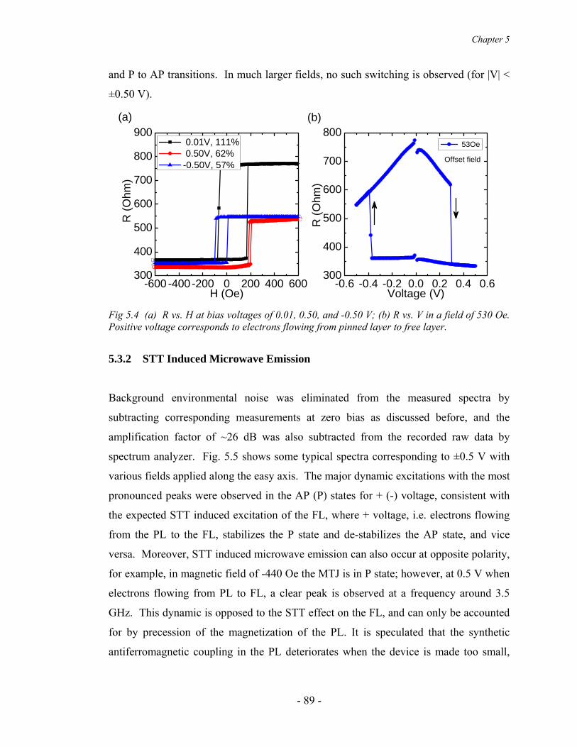
Chapter 5
and P to AP transitions. In much larger fields, no such switching is observed (for |V| <
±0.50 V).
-0.6 -0.4 -0.2 0.0 0.2 0.4 0.6300
400
500
600
700
800 53Oe
R (O
hm)
Voltage (V)
Offset field
-600 -400-200 0 200 400 600300
400
500
600
700
800
900
R
(Ohm
)
H (Oe)
0.01V, 111% 0.50V, 62% -0.50V, 57%
(a) (b)
Fig 5.4 (a) R vs. H at bias voltages of 0.01, 0.50, and -0.50 V; (b) R vs. V in a field of 530 Oe. Positive voltage corresponds to electrons flowing from pinned layer to free layer.
5.3.2 STT Induced Microwave Emission
Background environmental noise was eliminated from the measured spectra by
subtracting corresponding measurements at zero bias as discussed before, and the
amplification factor of ~26 dB was also subtracted from the recorded raw data by
spectrum analyzer. Fig. 5.5 shows some typical spectra corresponding to ±0.5 V with
various fields applied along the easy axis. The major dynamic excitations with the most
pronounced peaks were observed in the AP (P) states for + (-) voltage, consistent with
the expected STT induced excitation of the FL, where + voltage, i.e. electrons flowing
from the PL to the FL, stabilizes the P state and de-stabilizes the AP state, and vice
versa. Moreover, STT induced microwave emission can also occur at opposite polarity,
for example, in magnetic field of -440 Oe the MTJ is in P state; however, at 0.5 V when
electrons flowing from PL to FL, a clear peak is observed at a frequency around 3.5
GHz. This dynamic is opposed to the STT effect on the FL, and can only be accounted
for by precession of the magnetization of the PL. It is speculated that the synthetic
antiferromagnetic coupling in the PL deteriorates when the device is made too small,
- 89 -

Chapter 5
even though it works excellently in larger devices. Therefore, the so called PL, is no
longer ideally fixed but still harder to switch and process than that of the FL.
2 4 6 8 10 10
5
10
15
20
2
480Oe 144Oe -180Oe -554Oe -770Oe
Pow
er (n
V/H
z0.5 )
Frequency (GHz)
-0.5V,90deg
2 4 6 8 10 120
5
10
15
20
786Oe 635Oe 327Oe 6Oe -440Oe
Pow
er (n
V/H
z0.5 )
Frequency (GHz)
0.5V,90deg(a) (b)
Fig. 5.5 Typical spectra corresponding to ±0.5 V with various fields applied along easy axis. With large positive fields MTJ is in AP state, and with large negative fields in P state as shown by magnetoresistance loop.
Several other striking characteristics can be clearly seen from Fig. 5.5, e.g. there
usually exist multiple complex peaks, and bandwidths of these peaks are generally
broad. For the highest peak at -0.5 V with a field -180 Oe, the full width at half
maximum (FWHM) is about 0.71 GHz. The lowest power level for all the curves is
about 0.5 nV/Hz0.5 and can be considered as the intrinsic noise of the MTJ which
includes magnetic and shot noise contributions. The spectrum can be nicely shown in a
contour plot as in Fig. 5.6. Clear emissions occur in the AP state at 0.5 V and in the P
state at -0.5 V, which means that they derive from the STT induced precession in the
FL. Besides these strong emissions, though weak, there still exist other FL generated
emissions. In the opposite polarity, additional weak emissions due to the precession of
PL are also noticeable at 0.5 V for P state and -0.5 V for AP state.
By fitting each spectral trace with multiple Lorentizian functions, the peak
frequency f, the FWHM linewidth Δf, and the integrated power P of each excitation
mode can be derived. Fig 5.7 shows the field dependence of the peak frequency and
FWHM at 0.50 V and -0.5 V. In the case of the AP state, two excitation modes are
clearly observed and analyzed from the contour plot Fig. 5.6. At constant voltage, all
- 90 -
Chapter 5
the peaks’ frequency f and FWHM linewidth Δf are tunable with H for both P and AP
states. Frequency, f, increases with H according to the Kittel formula[20],
γ ππ
= + + +( )( 42 k kf H H H H M )s
where γ is the gyromagnetic ratio, Hk the anisotropic field, Ms the magnetization.
Fig. 5.6 Contour plots of spectra corresponding to ±0.5 V with various fields applied along easy axis. Dotted white lines divide the plots into P and AP state. Black downward arrow on right shows the field sweeping direction. Colorbar shows microwave power level in the unit of nV/Hz0.5.
Fig 5.7 Field dependence of peak frequency (open circle) and FWHM (solid triangle) at (a) 0.50 V and (b) -0.5 V.
However, the best fitting results with the Kittel equation always give much smaller
values of 4πMs than that in bulk Co40Fe40BB20, which is about 12 kOe. For example,
fitting to the peak AP 1 and P give a 4πMsts of 4.0 kOe and 3.2 kOe respectively. The
linewidth of the lower frequency mode (AP 1 ) does not change much with field. By
contrast, the higher frequency mode (AP 2 ) only shows weak dependence of the
linewidth in the low field regime. It becomes much broader in a field around 700 Oe
st
nd
200 300 400 500 600 700 8003.54.04.55.05.56.06.57.07.5
f (G
Hz)
H (Oe)
0.5V
0.30.60.91.21.51.82.12.42.73.0
Δf (
GH
z)
AP 1st
-800-700-600-500-400-300-200-1002.5
3.0
3.5
4.0
4.5
5.0
5.5
6.0
f (G
Hz)
H (Oe)
-0.5V
0.2
0.4
0.6
0.8
1.0
1.2
AP 2nd
Δf (
GH
z)
P
(a) (b)
- 91 -
Chapter 5
and the linewidth turns narrower again in the even higher field regime. For the
excitation mode in the P state, the linewidth is quite similar to that in AP 1 when the
field is larger than 200 Oe and it becomes much larger in a smaller field.
st
Fig. 5.8 shows the frequency f, FWHM linewidth Δf, and integrated power P as a
function of the bias voltage for the two excitation modes in the anti-parallel state with a
magnetic field of 236 Oe applied along the easy axis. From the voltage dependence of
power (Fig. 5.8(c)), the microwave emission is small when the bias voltage is low.
With increasing voltage, once above a threshold voltage around 0.3 V, the emission
power starts increasing dramatically. Finally a total power of about 3 nW can be easily
obtained even under modest bias conditions. The direction of the field is crucial to the
peak’s intensity, and a 10° field deviation around easy axis can increase the emission
power by a factor of 10, but this does not mean that more deviation always results in
larger emission although the largest emission does usually occur when the field is
applied along hard axis so that the cone angle of the precession is maximized, thus
giving rise to maximal resistance change in the device. Therefore, total power that is
delivered to a 50 Ω load can be as high as ~30 nW.
The bias dependence of the emission frequency (Fig. 5.8(a)) shows that the
frequency remains almost constant when the voltage is below the threshold value and
starts to decrease when the voltage exceeds the threshold, which demonstrates that the
frequency of the oscillator can be tuned only by an electrical voltage. The analysis of f
versus bias voltage confirms that the microwave emission peaks in Fig. 5.6(a) are
indeed steady state excitations above the critical threshold voltage and not thermally
excited ferromagnetic resonance modes (T-FMR). According to theory[21,22] and
experiment[14], the transition from T-FMR to steady state in-plane precession (IPP) can
be inferred from the evolution of the frequency f, linewidth Δf, and the output power P
of the microwave emission as a function of increasing bias voltage. The frequency of
the T-FMR mode is expected to change little at small voltages, but decrease moderately
near the critical voltage Vc, consistent with the spin-wave theory[10,23] and the
macrospin simulations[24]. This red-shift in frequency with bias voltage is a
characteristic of an IPP mode where the magnetization precesses around the sub-
threshold static equilibrium position[21,22]. If the device is driven harder by bias
- 92 -
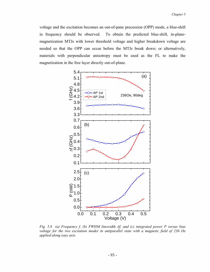
Chapter 5
voltage and the excitation becomes an out-of-pane precession (OPP) mode, a blue-shift
in frequency should be observed. To obtain the predicted blue-shift, in-plane-
magnetization MTJs with lower threshold voltage and higher breakdown voltage are
needed so that the OPP can occur before the MTJs break down; or alternatively,
materials with perpendicular anisotropy must be used as the FL to make the
magnetization in the free layer directly out-of-plane.
0.10.20.30.40.50.60.7
Δf (
GH
z)
3.33.63.94.24.54.85.15.4
AP 1st AP 2nd
f (
GH
z)
236Oe, 90deg
0.0 0.1 0.2 0.3 0.4 0.50.00.51.01.52.02.5
P (n
W)
Voltage (V)
(a)
(b)
(c)
Fig. 5.8 (a) Frequency f, (b) FWHM linewidth Δf, and (c) integrated power P versus bias voltage for the two excitation modes in antiparallel state with a magnetic field of 236 Oe applied along easy axis.
- 93 -

Chapter 5
By contrast, linewidth Δf versus bias voltage shows a minimum, and the occurrence
of the minimum is accompanied by an abrupt increase in power and a decrease in f, as
observed in Fig. 5.8. For the AP 1st mode, a relatively broad linewidth of ~0.45 GHz is
observed. The linewidth then narrows as the voltage in increased and reaches a
minimum at about 0.3 V, the same as determined from the current-induced-switching in
Fig. 5.4. As the voltage is increased further past this minimum point, a dramatic
broadening in the linewidth is seen. This characteristic is more pronounced in the AP
2nd mode than that in AP 1st mode (Fig. 5.8(b)). The initial narrowing in linewidth can
be understood from stochastic arguments. Below threshold, the dynamical state is
dominated by amplitude and phase fluctuations due to thermal noise, which results in
the broad spectral traces observed. As the current is increased, the amplitude of
precession increases and, as a consequence, the trajectories become more immune to
amplitude fluctuations which scale with temperature and not amplitude. In the limit of
large amplitude motion, in which only phase noise contributes, the spectral linewidth
can be estimated from stochastic spin-wave theory[24]. For the linewidth broadening
past the linewidth minimum, it is speculated to result from higher-order nonlinear
effects[14].
5.3.3 Sensitive Spectrum
Obtaining a nice microwave spectrum is nontrivial, and it is found that the spectrum can
vary dramatically from device to device, even for some identical-looking tunnel
junctions. For example, Fig. 5.9 shows both the field and current induced switching for
two devices, which are nominally same in both size and structure, and furthermore, they
are also close to each other on the same wafer. From these static measurements, the
behavior of both devices is almost identical: very similar resistance, TMR, coercivity
Hc, dipolar coupling, and even very close threshold voltage for current induced
switching. By contrast, their microwave emission spectra are distinctly different. For
Device II, a clear STT induced excitation is seen, though it only manifests itself near the
boundary between P and AP state where the FL becomes most easily excited by spin-
torque with the assistance of the applied field. However, for Device I, no such clear
- 94 -

Chapter 5
and nice microwave emission is detected, except some low frequency noise and some
non-coherent excitations with very broad linewidth at the AP/P state boundary which
might come from STT amplified magnetic noises at this critical point of field switching.
Therefore, there exist some non-obvious factors which can strongly influence
microwave emission, but field and current switching are not very much sensitive to.
The significant influence of the barrier roughness on the microwave emission has been
directly investigated using transmission electron microscopy (TEM). Two nominal
identical wafers with same multilayered structure are fabricated under same conditions.
However, from spectrum measurement, it turned out that the yield of obtaining clear
STT induced emission from one sample is far lower that the other one. TEM was
carried out on two typical devices, each on one wafer, using focused ion beam to cross-
section the active MTJs. The images show that the tunneling barrier of the sample with
low yield is much rougher than that of the other sample with high yield.
-0.6 -0.4 -0.2 0.0 0.2 0.4 0.6
1200
1500
1800
2100
2400
2700
3000
R (O
hm)
V (Volt)
Device I Device II
-600 -400-200 0 200 400 600
1200
1500
1800
2100
2400
2700
3000
R (O
hm)
H (Oe)
111% 113%
(a) (b)
Fig 5.9 (a) Field switching and (b) current induced switching of two nominally identical devices. Magnetoresistance loops are measured at 0.01 V, and voltage switching loops are obtained with magnetic fields applied to cancel the dipolar coupling, or the offset field in (a), respectively. Red (blue) curves are for Device I (II).
- 95 -
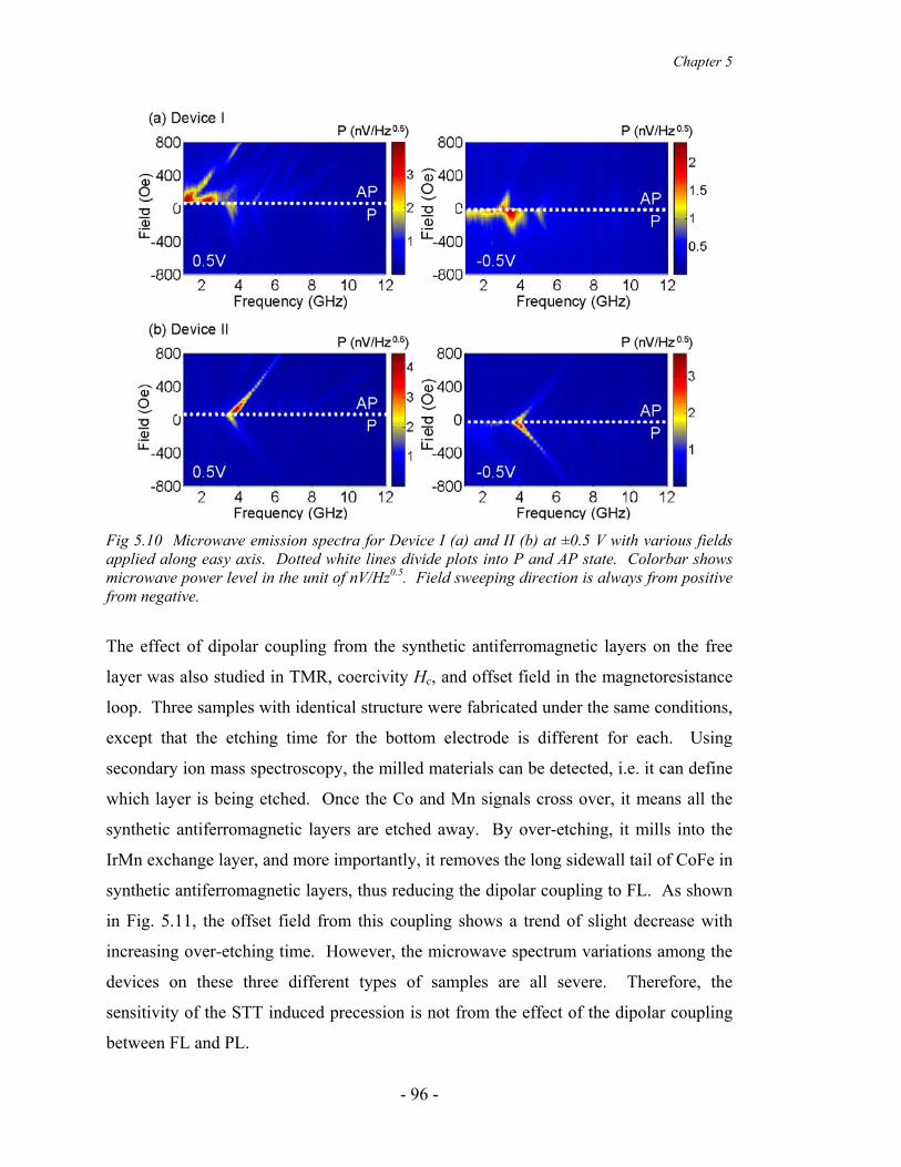
Chapter 5
Fig 5.10 Microwave emission spectra for Device I (a) and II (b) at ±0.5 V with various fields applied along easy axis. Dotted white lines divide plots into P and AP state. Colorbar shows microwave power level in the unit of nV/Hz0.5. Field sweeping direction is always from positive from negative.
The effect of dipolar coupling from the synthetic antiferromagnetic layers on the free
layer was also studied in TMR, coercivity Hc, and offset field in the magnetoresistance
loop. Three samples with identical structure were fabricated under the same conditions,
except that the etching time for the bottom electrode is different for each. Using
secondary ion mass spectroscopy, the milled materials can be detected, i.e. it can define
which layer is being etched. Once the Co and Mn signals cross over, it means all the
synthetic antiferromagnetic layers are etched away. By over-etching, it mills into the
IrMn exchange layer, and more importantly, it removes the long sidewall tail of CoFe in
synthetic antiferromagnetic layers, thus reducing the dipolar coupling to FL. As shown
in Fig. 5.11, the offset field from this coupling shows a trend of slight decrease with
increasing over-etching time. However, the microwave spectrum variations among the
devices on these three different types of samples are all severe. Therefore, the
sensitivity of the STT induced precession is not from the effect of the dipolar coupling
between FL and PL.
- 96 -
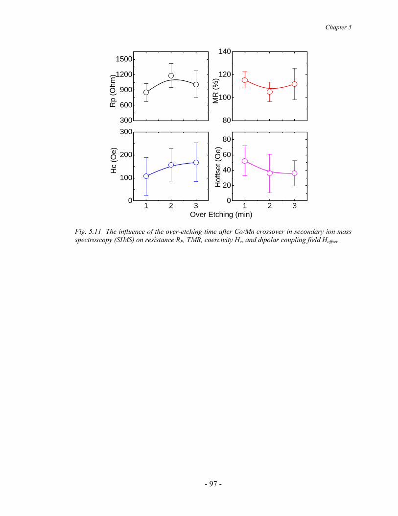
Chapter 5
300
600
900
1200
1500
Rp
(Ohm
)80
100
120
140
MR
(%)
1 2 30
100
200
300
Hc
(Oe)
Over Etching (min)1 2 3
0
20
40
60
80
Hof
fset
(Oe)
Fig. 5.11 The influence of the over-etching time after Co/Mn crossover in secondary ion mass spectroscopy (SIMS) on resistance RP, TMR, coercivity Hc, and dipolar coupling field Hoffset.
- 97 -

Chapter 5
5.4 DISCUSSION AND COMMENT
It has been demonstrated that current induced precessional excitations can produce
microwaves with power levels one to two orders of magnitude higher than in spin-valve
structures. The observation of much higher rf power emission from state of the art
MTJs is of high technological interest. Moreover, clear evidence has been found for the
STT induced excitation modes whose frequency, linewidth and power vary substantially
with applied field and bias voltage. The detailed control and understanding of the
frequency, linewidth and emission power is critical. In particular, it is important to
identify the factors which broaden the linewidth in MTJs, whether external, i.e. thermal,
or intrinsic.
From the experimental observations, the nature of the broad linewidth can be
hypothesized and a few comments will be discussed. In all these small nanopillar
samples, to control the resistance in a desirable low regime, the tunneling barriers have
to be very thin, only of about 1 nm thick. Roughness is inevitable in such ultrathin
tunnel barriers. In such a thin barrier, even a weak nonuniformity in barrier thickness
would cause strong local variations of the current density across the sample, which
could reduce the coherence of the magnetization dynamics and lead to a
nonhomogeneous excitation mode profile. The frequency of such a nonhomogeneous
mode differs then from a homogeneously excited mode, due to different dipolar and
exchange contributions[25]. Therefore, broad linewidth develops in the microwave
emission spectrum. The low magnetization values from the frequency fitting with field
could possibly be due to the nonhomogeneous excitations, which can not be well
accounted for by Kittel equation[23,26]. Studies in micromagnetic simulations might
reveal some more details about the nature of the linewidth broadening in these high
TMR samples. The complex physical processes behind this behavior are worthy of
further investigation. Despite of all the challenges, the experimental results clearly
demonstrate the high potential of MgO based MTJs as nano-oscillators for tunable rf
emission.
- 98 -
Chapter 5
REFERENCES:
[1] L. Berger, "Emission of spin waves by a magnetic multilayer traversed by a
current," Phys. Rev. B 54 (13), 9353 (1996).
[2] J. C. Slonczewski, "Current-driven excitation of magnetic multilayers," J. Magn.
Magn. Mater. 159, L1-L7 (1996).
[3] J. A. Katine, F. J. Albert, R. A. Buhrman, E. B. Myers, and D. C. Ralph,
"Current-Driven Magnetization Reversal and Spin-Wave Excitations in
Co/Cu/Co Pillars," Phys. Rev. Lett. 84 (14), 3149-3152 (2000).
[4] J. Hayakawa, S. Ikeda, Y. M. Lee, R. SasaKi, T. Meguro, F. Matsukura, H.
Takahashi, and H. Ohno, "Current-Driven Magnetization Switching in
CoFeB/MgO/CoFeB Magnetic Tunnel Junctions," Jpn. J. Appl. Phys. 44 (41),
L1267-L1270 (2005).
[5] H. Kubota, A. Fukushima, Y. Ootani, S. Yuasa, K. Ando, H. Maehara, K.
Tsunekawa, D. D. Djayaprawira, N. Watanabe, and Y. Suzuki, "Evaluation of
Spin-Transfer Switching in CoFeB/MgO/CoFeB Magnetic Tunnel Junctions,"
Jpn. J. Appl. Phys. 44 (40), L1237-L1240 (2005).
[6] G. Bertotti, C. Serpico, I. D. Mayergoyz, A. Magni, M. d'Aquino, and R. Bonin,
"Magnetization Switching and Microwave Oscillations in Nanomagnets Driven
by Spin-Polarized Currents," Phys. Rev. Lett. 94, 127206- (2005).
[7] O. Boulle, V. Cros, J. Grollier, L. G. Pereira, C. Deranlot, F. Petroff, G. Faini, J.
Barnas, and A. Fert, "Shaped angular dependence of the spin-transfer torque and
microwave generation without magnetic field," Nat. Phys. 3, 492 (2007).
[8] S. Kaka, M. R. Pufall, W. H. Rippard, T. J. Silva, S. E. Russek, and J. A. Katine,
"Mutual phase-locking of microwave spin torque nano-oscillators," Nature 437,
389 (2005).
[9] S. I. Kiselev, J. C. Sankey, I. N. Krivorotov, N. C. Emley, R. J. Schoelkopf, R.
A. Buhrman, and D. C. Ralph, "Microwave oscillations of a nanomagnet driven
by a spin-polarized current," Nature 425, 380 (2003).
- 99 -
Chapter 5
[10] S. M. Rezende, F. M. de Aguiar, R. L. Rodriguez-Suarez, and A. Azevedo,
"Mode Locking of Spin Waves Excited by Direct Currents in Microwave Nano-
oscillators," Phys. Rev. Lett. 98, 087202 (2007).
[11] M. Tsoi, A. G. M. Jansen, J. Bass, W.-C. Chiang, V. Tsoi, and P. Wyder,
"Generation and detection of phase-coherent current-driven magnons in
magnetic multilayers," Nature 406, 46 (2000).
[12] I. N. Krivorotov, N. C. Emley, J. C. Sankey, S. I. Kiselev, D. C. Ralph, and R.
A. Buhrman, "Time-Domain Measurements of Nanomagnet Dynamics Driven
by Spin-Transfer Torques," Science 307, 228 (2005).
[13] I. N. Krivorotov, D. V. Berkov, N. L. Gorn, N. C. Emley, J. C. Sankey, D. C.
Ralph, and R. A. Buhrman, "Large-amplitude coherent spin waves excited by
spin-polarized current in nanoscale spin valves," Phys. Rev. B 76, 024418
(2007).
[14] Q. Mistral, J.-V. Kim, T. Devolder, P. Crozat, C. Chappert, J. A. Katine, M. J.
Carey, and K. Ito, "Current-driven microwave oscillations in current
perpendicular-to-plane spin-valve nanopillars," Appl. Phys. Lett. 88, 192507
(2006).
[15] S. S. P. Parkin, C. Kaiser, A. F. Panchula, P. Rice, M. G. Samant, S.-H. Yang,
and B. Hughes, "Giant tunneling magnetoresistance at room temperature with
MgO (100) tunnel barriers," Nature Materials 3, 862 (2004).
[16] A. M. Deac, A. Fukushima, H. Kubota, H. Maehara, Y. Suzuki, S. Yuasa, Y.
Nagamine, K. Tsunekawa, D. D. Djayaprawira, and N. Watanabe, "Bias-driven
high-power microwave emission from MgO-based tunnel magnetoresistance
devices," Nat. Phys. 4, 803 (2008).
[17] D. Houssameddine, U. Ebels, B. Delaet, B. Rodmacq, I. Firastrau, F. Ponthenier,
M. Brunet, C. Thirion, J. P. Michel, L. Prejbeanu-Buda, M. C. Cyrille, O.
Redon, and B. Dieny, "Spin-torque oscillator using a perpendicular polarizer and
a planar free layer," Nat. Mater. 6, 447 (2007).
[18] A. V. Nazarov, H. M. Olson, H. Cho, K. Nikolaev, Z. Gao, S. Stokes, and B. B.
Pant, "Spin transfer stimulated microwave emission in MgO magnetic tunnel
junctions," Appl. Phys. Lett. 88, 162504 (2006).
- 100 -

Chapter 5
[19] A. V. Nazarov, K. Nikolaev, Z. Gao, H. Cho, and D. Song, "Microwave
generation in MgO magnetic tunnel junctions due to spin transfer effects
(invited)," J. Appl. Phys. 103, 07A503 (2008).
[20] C. Kittel, "Introduction to Solid State Physics," (John Wiley & Sons, 2005).
[21] J.-V. Kim, Q. Mistral, C. Chappert, V. S. Tiberkevich, and A. N. Slavin, "Line
Shape Distortion in a Nonlinear Auto-Oscillator Near Generation Threshold:
Application to Spin-Torque Nano-Oscillators," Phys. Rev. Lett. 100, 167201
(2008).
[22] V. Tiberkevich, A. Slavin, and J.-V. Kim, "Microwave power generated by a
spin-torque oscillator in the presence of noise," Appl. Phys. Lett. 91, 192506
(2007).
[23] A. N. Slavin and P. Kabos, "Approximate theory of microwave generation in a
current-driven magnetic nanocontact magnetized in an arbitrary direction," IEEE
Trans. Magn. 41, 1264 (2005).
[24] J.-V. Kim, "Stochastic theory of spin-transfer oscillator linewidths," Phys. Rev.
B 73, 174412 (2006).
[25] B. A. Kalinikos and A. N. Slavin, "Theory of dipole-exchange spin wave
spectrum for ferromagnetic films with mixed exchange boundary conditions," J.
Phys. C 19, 7013 (1986).
[26] K.-J. Lee, A. Deac, O. Redon, J.-P. Nozieres, and B. Dieny, "Excitations of
incoherent spin-waves due to spin-transfer torque," Nat. Mater. 3, 877 (2004).
- 101 -
Chapter 5
- 102 -

Chapter 6
Chapter 6
CONCLUSIONS AND SUGGESTIONS FOR FURTHER RESEARCH
- 103 -

Chapter 6
6.1 CONCLUSIONS
The research performed in this dissertation was aimed at deepening the understanding
of spin polarized current phenomena in magnetic tunnel junctions, with emphasis on
both tunneling magnetoresistance and spin-transfer torque effect. Increased tunneling
magnetoresistance from amorphous CoFe was studied. Cross-section transmission
electron microscopy revealed that films of CoFe alloys, sandwiched between two
conventional amorphous materials, undergo an amorphous-to-crystalline transition at a
critical thickness of ~25-30 Å. With these thin amorphous layers as an electrode in
Al2O3 magnetic tunnel junctions, significant enhancement in tunneling
magnetoresistance and tunneling spin polarization was found compared to when
crystalline layers were used. To understand this phenomenon, both x-ray emission
spectroscopy and ab initio calculations were carried out to investigate the electronic
structures of both amorphous and crystalline CoFe. Although calculation results of
crystalline and amorphous forms of bulk CoFe alloys show substantial differences in
their band structures, the calculated spin polarization at the Fermi energy is reduced for
amorphous, contrary to an explanation of the experimental observation in terms of the
bulk electronic states. From the calculations, it is also found that the spin moment of
the Fe element is more sensitive to its local chemical and structural environment.
Indeed, x-ray emission spectroscopy shows a significant increase in the Fe, but not the
Co, 3d density of states at the Fermi energy for thin amorphous CoFe layers. Therefore,
it is reasonable to postulate that the increased tunneling magnetoresistance is likely due
to changes in electronic structure and interfacial bonding at the Al2O3/CoFe interface
caused by amorphization induced atomic relaxation.
The tunneling anisotropic magnetoresistance of MgO and Al2O3 tunnel junctions
with 3d transition metal alloys was investigated. Despite the small effect due to weak
spin-orbit coupling in these systems, complex dependences of the junction resistance on
the bias voltage and angle were found, which are distinctly different for MgO and Al2O3
tunnel barriers. A tight-binding model suggests that the tunneling anisotropic effect
derives from the anisotropy in the interface density of states of the majority band due to
mixing with a resonant state via spin-orbit coupling. Moreover, a puzzling reversal in
- 104 -

Chapter 6
tunneling anisotropic magnetoresistance effect from CrMo has also been observed.
Further work will be required to investigate and understand this effect from an
antiferromagnetic material.
Besides the studies in tunneling magnetoresistance effect, spin transfer torque
induced microwave emission from magnetic tunnel junctions has been explored. It is
shown that, compared to spin-valves, much higher microwave power is emitted from
nano-fabricated tunnel junctions with MgO tunnel barriers which exhibit high tunneling
magnetoresistance at low resistance-area values. However, accompanied with the
increased power, it is also found that the linewidth of the emission is usually large, and
the spectral features vary sensitively from device to device. Preliminary investigations
suggest that both the broad linewidth and the variations in the spectrum are possibly due
to non-uniform spatial magnetic excitation arising from inhomogeneous current flow
through the tunnel barrier, since the barrier is so thin that any film roughness would
cause severe variation in the local resistance and current flow.
The results discussed in this dissertation are of importance in both physics and
technology. The studies in the tunneling magnetoresistance deepen the understanding
of the complicated spin dependent tunneling process in magnetic tunnel junctions, and
the research in spin transfer torque has the potential to be relevant for device
applications such as STT-RAM and rf nano-oscillator. Spintronic devices using
magnetic tunnel junctions have been successfully incorporated in recording read heads,
thus continuing to dramtically lower the price and increase the storage capacity of hard
disk drives. The 16Mbit MRAM has been released to the market and a 32Mbit STT-
RAM has just been demonstrated and its commercial availability seems imminent.
Beyond these, innovative Racetrack Memory has been proposed and is being researched
to use spin polarized currents to move magnetic domains along a nanowire, where as
current is passed through the domains pass by magnetic read/write heads positioned
near the wire so that patterns of bits can be read or written. If it is developed
successfully, Racetrack Memory would offer storage density higher than comparable
solid-state memory devices like Flash RAM and similar to conventional disk drives, but
with much higher read/write performance. All these promising prospects make it,
- 105 -

Chapter 6
together with MRAM and STT-RAM, one of a number of new technologies vying to
become a universal memory in the future.
6.2 SUGGESTIONS FOR FURTHER RESEARCH
Some unresolved issues in this dissertation are worthy of further investigations. For
example, large tunneling anisotropic magnetoresistance is desirable at room temperature
for potential applications in information storage and field sensing, especially when only
a single ferromagnetic layer is present. To achieve this, materials with strong spin-orbit
coupling, e.g. Co/Pt multilayers, should be explored. In Cr based systems, where spin
density waves play a very important role in their transport properties, correlating the
tunneling anisotropic magnetoresistance with the spin density wave will be an
interesting experimental topic. In the area of spin transfer torque, there remain many
exploratory topics that are still unresolved. Lowering the critical current density to
switch the free layer is of immediate and critical importance, and many materials with
perpendicular magnetic anisotropy are being studied. A clever design of the device
structure with the commonly used materials may also be a solution. Further increase in
the rf emission power is desired, and a complete understanding of the broad emission
linewidth is both scientifically and technologically critical to this research field.
Besides the above, many other topics are of great interest. Successful demonstration
of spin logic devices will enrich the applications of spintronics. Nonlocal lateral
devices and three terminal devices could open a new door to integrate spintronics with
conventional CMOS technology. Electrical field control of magnetism is certainly very
attractive, such as in multiferroic materials that are both ferroelectric and magnetic. The
combination of spintronics with exotic oxides is quite challenging, but extremely
stimulating. Research on these topics will establish fundamentally new approaches to
understand and control the wealth of electronic, spin, and collective mode excitations
associated with complex oxide interfaces.
- 106 -

Appendix
APPENDIX: LIST OF ACRONYMS
AF (FM) Antiferromagnetic (Ferromagnetic)
AFM Atomic Force Microscopy
AP (P) Antiparallel (Parallel)
CFB CoFeB Alloy
CFB10 Co63Fe27BB10
CFB20 Co40Fe40BB20
CFB30 Co49Fe21BB30
DOS Density of States
EELS Electron Energy Loss Spectroscopy
FL (PL) Free (Pinned) Layer
FM (AF) Ferromagnetic (Antiferromagnetic)
FMR Ferromagnetic Resonance
FWHM Full Width at Half Maximum
GGA Generalized Gradient Approximation
GMR Giant Magnetoresistance
IBD Ion Beam Deposition
IETS Inelastic Electron Tunneling Spectroscopy
IPP (OPP) In-Plane (Out-of-Plane) Procession
LLG Landau-Lifshitz-Gilbert
MD Molecular Dynamics
MRAM Magnetic Random Access Memory
MTJ Magnetic Tunnel Junction
NMP N-Methyl-2-Pyrrolidone
NXES Non-resonant X-ray Emission Spectroscopy
OPP (IPP) Out-of-Plane (In-Plane) Procession
P (AP) Parallel (Antiparallel)
PL (FL) Pinned (Free) Layer
RA Resistance-Area Product
RBS Rutherford Backscattering Spectroscopy
- 107 -

Appendix
RF Radio-Frequency
RIXS Resonant Inelastic X-ray Emission Spectroscopy
SCF Sandwiched CoFe Layer
SEM Scanning Electron Microscopy
SIMS Secondary Ion Mass Spectrometry
SOC Spin Orbit Coupling
SQUID Superconducting Quantum Interference Device
STS Superconducting Tunneling Spectroscopy
STT Spin Transfer Torque
TAMR Tunneling Anisotropic Magnetoresistance
TEM Transmission Electron Microscopy
T-FMR Thermally Excited Ferromagnetic Resonance
TM Transition Metal
TMR Tunneling Magnetoresistance
TSP Tunneling Spin Polarization
VASP Vienna Ab-initio Simulation Package
VSM Vibrating Sample Magnetometry
XES X-ray Emission Spectroscopy
XPS X-ray Photoelectron Spectroscopy
XRD X-ray Diffraction
- 108 -