spin accumulation in coupled quantum dots with ferromagnetic and superconducting electrodes
TRANSCRIPT
ARTICLE IN PRESS
Physica B 403 (2008) 3125– 3129
Contents lists available at ScienceDirect
Physica B
0921-45
doi:10.1
� Corr
E-m
journal homepage: www.elsevier.com/locate/physb
Spin accumulation in coupled quantum dots with ferromagneticand superconducting electrodes
Hui Pan a,�, Rong Lu b
a Department of Physics, Beijing University of Aeronautics and Astronautics, Beijing 100083, Chinab Center for Advanced Study, Tsinghua University, Beijing 100084, China
a r t i c l e i n f o
Article history:
Received 4 March 2008
Received in revised form
17 March 2008
Accepted 24 March 2008
PACS:
73.23.�b
73.63.Kv
72.25.Dc
74.45.þc
Keywords:
Spin accumulation
Coupled quantum dots
Andreev reflection
Ferromagnetic electrodes
26/$ - see front matter & 2008 Elsevier B.V. A
016/j.physb.2008.03.022
esponding author. Fax: +86 10 82317935.
ail address: [email protected] (H. Pan).
a b s t r a c t
We theoretically investigate the spin accumulation in two parallel coupled quantum dots (QDs) with
ferromagnetic and superconducting electrodes. Due to the ferromagnetic lead, the spin accumulation
appears on the resonance of Andreev reflection. The spin accumulation in each of the two QDs can be
controlled by the gate voltage. The sign of the spin accumulation is also controllable by tuning the bias.
Furthermore, tuning the magnetic flux can exchange the amplitude of the spin accumulation in the two
QDs. The Aharonov–Bohm oscillation effects also provides a way to control the spin accumulation
of each QD.
& 2008 Elsevier B.V. All rights reserved.
1. Introduction
In the resonant tunneling through a quantum dot (QD) system,the phase coherence of electrons can be sustained. Interferenceexperiments with an Aharonov–Bohm (AB) ring containing oneQD have been done to detect the quantum phase coherence [1–5].More recently, an AB interferometer containing two coupled QDswith a QD inserted in each arm has been studied in experiments[6,7]. In such parallel-coupled double quantum dot (DQD) system,the two coupled QDs can form the bonding and antibondingstates. The possibility to control each of the two QDs separatelymakes the quantum transport phenomena rich and varied [8–10].As a controllable two-level system, the DQD system thereforebecomes one of the promising candidates as a quantum bit inquantum computation based on solid-state devices [11].
On the other hand, the superconductor coupled mesoscopichybrid systems have become an interesting field in recent yearsbecause of both the fundamental physics and the potentialapplications for future nanoelectronics [12–17]. The Andreevreflection happens at the normal-metal/superconductor (N/S)
ll rights reserved.
interface [18]. Another interesting hybrid system consists offerromagnet (F) and superconductor (S) leads coupled with anormal QD (F/QD/S). The left ferromagnetic lead introduces spin-dependent tunneling rates between the lead and the centralregion. This results in a nonzero net spin in the central region,which is called as the spin accumulation or spin imbalance. Anefficient method for writing spin in the F/QD/S system has beenprovided based on the spin-accumulation mechanism caused bythe Andreev reflection [19]. The spin accumulation affects severaltransport properties, such as magnetoresistance, differentialresistance, and the zero-bias anomaly [20,21]. Therefore, the spinaccumulation can be detected through the related experiments.The spin-flip effects on the F/QD/S system has also been studiedtheoretically and a double-peak resonance has been found [22].
However, the spin accumulations in the parallel-coupled DQDsystems are still less studied. Can the spin accumulation in each ofthe two QDs be controlled by the gate voltage and the magneticflux? Motivated by this, we investigate the spin accumulation inthe F/DQD/S system in this work. In the context of intensiveresearch and impressive progress in F/S hybrid structures [23], theproposed F/DQD/S system should be feasible with up-to-datenanotechnology. Furthermore, the spin coherence time in semi-conductors is orders longer than charge coherence time, whichcan exceed 100 ns at low temperature [24,25]. We look forward to
ARTICLE IN PRESS
H. Pan, R. Lu / Physica B 403 (2008) 3125–31293126
hearing the relevant experimental response. By using the none-quilibrium Green’s function (NGF) techniques [19,26–28], we haveanalyzed the spin accumulation in the two QDs. The spinaccumulation in the two QDs can be easily controlled by the gatevoltage. The sign of the spin accumulation is also controllable bytuning the bias. Furthermore, tuning the magnetic flux can swapthe spin accumulation status of the two QDs. The spin accumula-tion also shows the AB oscillations with the magnetic flux, whichprovides another way to control the spin accumulation of the QDs.
The rest of this paper is organized as follows. In Section 2 wepresent the model Hamiltonian and derive the formula of theelectron occupation number and the spin accumulation in eachQD by using the NGF technique. In Section 3 we study the effectsof the gate voltage, the bias, and the magnetic flux on the spinaccumulation in the QDs. The control of the magnitude and sign ofthe spin accumulation are discussed in detail. Finally, a briefsummary is given in Section 4.
2. Physical model and formula
In the F/DQD/S system under consideration, an AB ringcontaining two coupled QDs, with one QD inserted in each arm,is connected with one ferromagnetic and one superconductinglead. The system is modeled by the following Hamiltonian
H ¼ HL þ HR þ HD þ HT, (1)
where
HL ¼Xks
ð�k þ sMÞayksaks, (2)
HR ¼Xps
�pbypsbps þX
p
½Dbyp"by
�p# þ H:c:�, (3)
HD ¼X
s;i¼1;2
ðei � eVgiÞdy
isdis �Xs
ðtceiydy1sd2s þ H:c:Þ, (4)
HT ¼X
ks;i¼1;2
ðtLiseifLi dyisaks þ H:c:Þ
þX
ps;i¼1;2
ðtRieifRi dyisbps þ H:c:Þ. (5)
HL describes the left ferromagnetic lead under the mean-fieldapproximation with an internal magnetic moment ~M. The tiltangle between the magnetic moment and the F/DQD interface hasbeen chosen to be zero [19,22]. HR is the standard BCSHamiltonian for the right superconducting lead with the energygap D. HD models the parallel-coupled DQDs where dyis ðdisÞ
represents the creation (annihilation) operator of the electron inthe QD i ði ¼ 1;2Þwith spin s and energy ei. tc denotes the interdotcoupling strength. The phase shift due to the total magnetic fluxthreading into the AB ring is assumed to be f ¼ 2pðfR þ fLÞ=f0,where fL ðfRÞ is the magnetic flux threading the left (right)subring and f0 ¼ hc=e. The flux difference between the left andright subrings is y ¼ pðfR � fLÞ=f0. HT represents the tunnelingcoupling between the DQD and leads. Because of the rightsuperconducting lead, it is convenient to use the 4� 4 Namburepresentation to include the physics of Andreev reflection. Thematrix of the hopping elements is defined as
ta ¼
ta1eifa1 0 0 0
0 �t�a1e�ifa1 0 0
0 0 ta2eifa2 0
0 0 0 �t�a2e�ifa2
0BBBB@
1CCCCA, (6)
where tai is the hopping strength and fL1 ¼ �fL2 ¼ �fR1 ¼
fR2 ¼ �f=4.
The retarded and lesser Green’s function are defined as
Grðt; t0Þ ¼ �iyðt � t0ÞhfCðtÞ;Cyðt0Þgi, (7)
and
Goðt; t0Þ ¼ ihCyðt0ÞCðtÞi, (8)
respectively, with the operator C ¼ ðdy1"; d1#; dy
2";d2#Þy. Let grð�Þ
and Grð�Þ denote the Fourier-transformed retarded Green’s func-
tion of the QD without and with the coupling to the leads. In theNambu representation, grð�Þ can be written as
½grð�Þ��1
¼
�� e1" þ i0þ 0 tceiy 0
0 �þ e1# þ i0þ 0 �tce�iy
tce�iy 0 �� e2" þ i0þ 0
0 �tceiy 0 �þ e2# þ i0þ
0BBBBBB@
1CCCCCCA
.
(9)
The retarded self-energies for the left ferromagnet and rightsuperconductor leads under the wide-bandwidth approximationare derived as [29]
RrLðeÞ ¼
Xk
t�LgrkðeÞtL
¼ �i
2
GL1" 0
ffiffiffiffiffiffiffiffiffiffiffiffiffiffiffiffiGL
1"GL2"
qeif=2 0
0 GL1# 0
ffiffiffiffiffiffiffiffiffiffiffiffiffiffiffiffiGL
1#GL2#
qe�if=2
ffiffiffiffiffiffiffiffiffiffiffiffiffiffiffiffiGL
1"GL2"
qe�if=2 0 GL
2" 0
0ffiffiffiffiffiffiffiffiffiffiffiffiffiffiffiffiGL
1#GL2#
qeif=2 0 GL
2#
0BBBBBBBBBB@
1CCCCCCCCCCA
,
ð10Þ
and
RrRðeÞ ¼
Xk
t�RgrpðeÞtR
¼ �i
2rð�Þ
GR1 �GR
1e�if=2D�
ffiffiffiffiffiffiffiffiffiffiffiGR
1GR2
qe�if=2 �
ffiffiffiffiffiffiffiffiffiffiffiGR
1GR2
q D�
�GR1eif=2D
�GR
1 �
ffiffiffiffiffiffiffiffiffiffiffiGR
1GR2
q D�
ffiffiffiffiffiffiffiffiffiffiffiGR
1GR2
qeif=2
ffiffiffiffiffiffiffiffiffiffiffiGR
1GR2
qeif=2 �
ffiffiffiffiffiffiffiffiffiffiffiGR
1GR2
q D�
GR2 �GR
2eif=2D�
�
ffiffiffiffiffiffiffiffiffiffiffiGR
1GR2
q D�
ffiffiffiffiffiffiffiffiffiffiffiGR
1GR2
qe�if=2 �GR
2e�if=2D�
GR2
0BBBBBBBBBBBB@
1CCCCCCCCCCCCA
,
ð11Þ
where grkðpÞðeÞ is the exact Green function of the left (right) lead
without the coupling to the DQD. The factor rRð�Þ is defined as [29]
rRð�Þ ¼ j�j=ffiffiffiffiffiffiffiffiffiffiffiffiffiffiffiffiffiffiffið�2 � D2Þ
qfor j�j4D and rRð�Þ ¼ �=i
ffiffiffiffiffiffiffiffiffiffiffiffiffiffiffiffiffiffiffiðD2 � �2Þ
qfor
j�joD. GLis is the linewidth function defined by GL
is ¼ 2prLst�LitLi
with rLs being the spin-dependent density of states of thecorresponding left lead, which represents the coupling betweenthe ith QD and the left ferromagnetic lead. With the definition of
the spin polarization of the left lead P � ðGLi" � GL
i#Þ=ðGLi" þ GL
i#Þ, the
coupling can be expressed as GLi" ¼ GL
i ð1þ PÞ and GLi# ¼ GL
i ð1� PÞ
with GLi ¼ ðG
Li" þ GL
i#Þ=2. Similarly, GRi is the linewidth function
defined by GRi ¼ 2prRt�RitRi, where rR is the density of states in the
right lead when it is in normal state.By using the Dyson equation, the retarded Green function of
the system can be obtained as
Grð�Þ ¼ ½grð�Þ�1
� Rrð�Þ��1, (12)
where
Rrð�Þ ¼ RrLð�Þ þ Rr
Rð�Þ. (13)

ARTICLE IN PRESS
H. Pan, R. Lu / Physica B 403 (2008) 3125–3129 3127
The lesser Green function of the system can be obtained by usingthe Keldysh equation
Goð�Þ ¼ Gr
ð�ÞRoð�ÞGað�Þ, (14)
where
Roð�Þ ¼Xa¼L;R
Roa ð�Þ ¼
Xa¼L;R
fað�Þ½Raað�Þ � Rr
að�Þ�, (15)
and Raa ¼ ðR
raÞy. fa is the 4� 4 Fermi distribution function matrix
in the generalized Nambu representation with f a;ij ¼ dijf ð�þ
ð�1ÞimaÞ. The chemical potentials are mL ¼ eV and mR ¼ 0, with eV
the bias. The expectation values of the electron occupationnumber nis ¼ dyisdis are given by
hn1"i ¼
Zdo2p
Im Go11, (16)
hn1#i ¼ 1�
Zdo2p
Im Go22. (17)
Similarly, hn2"i and hn2#i can be calculated from Go33 and Go
44,respectively. The spin accumulation is defined as
Dni ¼ hni"i � hni#i. (18)
In the following calculations, we take D ¼ 1 as the energy unit andset _ ¼ e ¼ 1.
3. Results and discussions
In this section, we perform the numerical calculations at zerotemperature. The dependence of the electron occupation number
0.00
0.25
0.50
0.0
0.5
1.00.0
0.5
1.0
Δn1,2
<n1σ>
<n2σ>
Vg/Δ
-0.6 0.60.40.20.0-0.2-0.4
-0.6 0.60.40.20.0-0.2-0.4
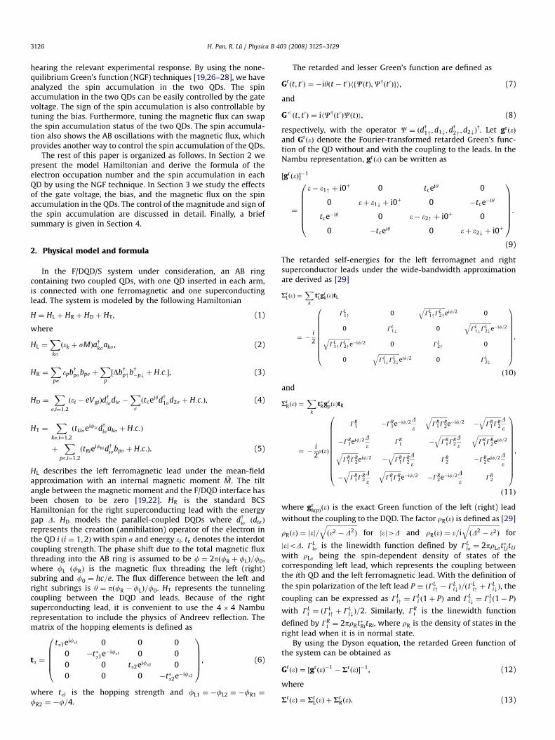
Fig. 1. (a) hn1si and (b) hn2si vs Vg for spin-up (solid line) and spin-down (dashed line) e
(f) are the corresponding ones at V ¼ �0:4. Other parameters are GL1" ¼ GL
2" ¼ 0:015, G
hnisi and the corresponding spin accumulation Dni for QD i
(i ¼ 1;2) on the gate voltage Vg, the bias V, and the magnetic fluxf are discussed in detail. Fig. 1 presents the dependence of hnii
and Dni on Vg at e1 ¼ �e2 ¼ 0:2 for V ¼ 0:4 and �0:4, respectively.We first discuss the case of V ¼ 0:4. There is a step from 0 to 1 inhn1si at Vg ¼ e1 � V ¼ �0:2 as shown in Fig. 1(a), indicating anelectron filling when e1 lines up with the chemical potentials mL ofthe ferromagnetic lead. In the curve for hn2si as shown in Fig. 1(b),the step is shifted to Vg ¼ e2 � V ¼ �0:6. In these curves, tworesonant dips emerge whose positions are pinned at Vg ¼ 0 and0:2 in hn1si, and at Vg ¼ �0:2 and 0 in hn2si, respectively.Furthermore, ni" and ni# are separated dramatically at these dips.These spin accumulations arecaused by the Andreev reflections.When e1 (e2) lines up with mR at Vg ¼ �0:2 (Vg ¼ 0:2), resonantAndreev reflection may occur in which a spin-up and a spin-downelectron in QD can leak into the superconductor lead by forming aCooper pair. When Vg ¼ 0, e1 and e2 are symmetrical about mR andare both below mL, which can also lead to Andreev reflection. Anelectron incident with appropriate energy can tunnel from the leftlead into the QD state e1 (e2), and then can be Andreev reflected asa hole back to the QD state e2 (e1). Since the ferromagnetic leadcan provide more spin-up electrons than spin-down electrons, thespin-down electrons will be depleted by the spin-up electrons inthe process of Andreev reflection, resulting in a spin accumulationDni40 in the QDs. As shown in Fig. 1(c), QD 1 or 2 can be spinpolarized at Vg ¼ 0:2 or �0:2, respectively. Furthermore, both QD1 and 2 can be spin polarized at Vg ¼ 0. It means that whether thespin accumulation in each of the two QDs can be easily controlledby Vg. For the case of V ¼ �0:4 as shown in Fig. 1(d)–(f), a Cooperpair is converted into a spin-up and a spin-down electron in the
0.0
0.5
1.0
0.0
0.5
1.0
-0.50
-0.25
0.00
Vg/Δ-0.6 0.60.40.20.0-0.2-0.4
-0.6 0.60.40.20.0-0.2-0.4
lectrons at V ¼ 0:4. (c) Dn1 (solid line) and Dn2 (dashed line) vs Vg at V ¼ 0:4. (d) toL1# ¼ GL
2# ¼ 0:05, GR1 ¼ GR
2 ¼ 0:1.
ARTICLE IN PRESS
-0.6
-0.2
0.0
0.2
-0.4
0.0
0.4
-0.4
0.0
0.4
-0.4
0.0
0.4
-0.2
0.0
0.2
-0.4
0.0
0.4
Δn1,2
eV/ΔeV/Δ0.60.40.20.0-0.2-0.4 -0.6 0.60.40.20.0-0.2-0.4
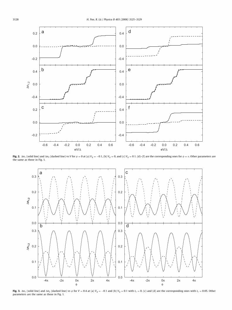
Fig. 2. Dn1 (solid line) and Dn2 (dashed line) vs V for f ¼ 0 at (a) Vg ¼ �0:1, (b) Vg ¼ 0, and (c) Vg ¼ 0:1. (d)–(f) are the corresponding ones for f ¼ p. Other parameters are
the same as those in Fig. 1.
0.0
0.1
0.2
0.3
0.0
0.1
0.2
0.3
0.0
0.1
0.2
0.3
-4π 4π2π0π-2π0.0
0.1
0.2
0.3
Δn1,2
Δn1,2
φ-4π 4π2π0π-2π
φ
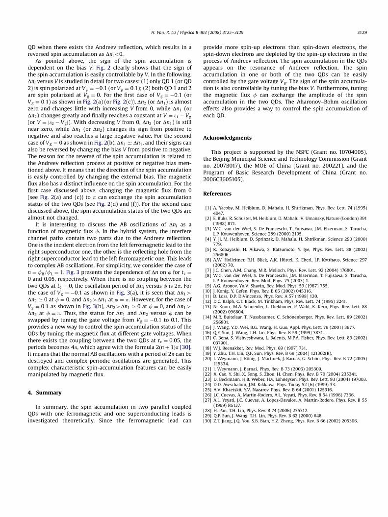
Fig. 3. Dn1 (solid line) and Dn2 (dashed line) vs f for V ¼ 0:4 at (a) Vg ¼ �0:1 and (b) Vg ¼ 0:1 with tc ¼ 0. (c) and (d) are the corresponding ones with tc ¼ 0:05. Other
parameters are the same as those in Fig. 1.
H. Pan, R. Lu / Physica B 403 (2008) 3125–31293128
ARTICLE IN PRESS
H. Pan, R. Lu / Physica B 403 (2008) 3125–3129 3129
QD when there exists the Andreev reflection, which results in areversed spin accumulation as Dnio0.
As pointed above, the sign of the spin accumulation isdependent on the bias V. Fig. 2 clearly shows that the sign ofthe spin accumulation is easily controllable by V. In the following,Dni versus V is studied in detail for two cases: (1) only QD 1 (or QD2) is spin polarized at Vg ¼ �0:1 (or Vg ¼ 0:1); (2) both QD 1 and 2are spin polarized at Vg ¼ 0. For the first case of Vg ¼ �0:1 (orVg ¼ 0:1) as shown in Fig. 2(a) (or Fig. 2(c)), Dn2 (or Dn1) is almostzero and changes little with increasing V from 0, while Dn1 (orDn2) changes greatly and finally reaches a constant at V ¼ e1 � Vg
(or V ¼ je2 � Vgj). With decreasing V from 0, Dn2 (or Dn1) is stillnear zero, while Dn1 (or Dn2) changes its sign from positive tonegative and also reaches a large negative value. For the secondcase of Vg ¼ 0 as shown in Fig. 2(b), Dn1 ’ Dn1, and their signs canalso be reversed by changing the bias V from positive to negative.The reason for the reverse of the spin accumulation is related tothe Andreev reflection process at positive or negative bias men-tioned above. It means that the direction of the spin accumulationis easily controlled by changing the external bias. The magneticflux also has a distinct influence on the spin accumulation. For thefirst case discussed above, changing the magnetic flux from 0(see Fig. 2(a) and (c)) to p can exchange the spin accumulationstatus of the two QDs (see Fig. 2(d) and (f)). For the second casediscussed above, the spin accumulation status of the two QDs arealmost not changed.
It is interesting to discuss the AB oscillations of Dni as afunction of magnetic flux f. In the hybrid system, the interferechannel paths contain two parts due to the Andreev reflection.One is the incident electron from the left ferromagnetic lead to theright superconductor one, the other is the reflecting hole from theright superconductor lead to the left ferromagnetic one. This leadsto complex AB oscillations. For simplicity, we consider the case ofn ¼ fR=fL ¼ 1. Fig. 3 presents the dependence of Dn on f for tc ¼
0 and 0.05, respectively. When there is no coupling between thetwo QDs at tc ¼ 0, the oscillation period of Dni versus f is 2p. Forthe case of Vg ¼ �0:1 as shown in Fig. 3(a), it is seen that Dn14Dn2 ’ 0 at f ¼ 0, and Dn24Dn1 at f ¼ p. However, for the case ofVg ¼ 0:1 as shown in Fig. 3(b), Dn24Dn1 ’ 0 at f ¼ 0, and Dn14Dn2 at f ¼ p. Thus, the status for Dn1 and Dn2 versus f can beswapped by tuning the gate voltage from Vg ¼ �0:1 to 0.1. Thisprovides a new way to control the spin accumulation status of theQDs by tuning the magnetic flux at different gate voltages. Whenthere exists the coupling between the two QDs at tc ¼ 0:05, theperiods becomes 4p, which agree with the formula 2ðnþ 1Þp [30].It means that the normal AB oscillations with a period of 2p can bedestroyed and complex periodic oscillations are generated. Thiscomplex characteristic spin-accumulation features can be easilymanipulated by magnetic flux.
4. Summary
In summary, the spin accumulation in two parallel coupledQDs with one ferromagnetic and one superconducting leads isinvestigated theoretically. Since the ferromagnetic lead can
provide more spin-up electrons than spin-down electrons, thespin-down electrons are depleted by the spin-up electrons in theprocess of Andreev reflection. The spin accumulation in the QDsappears on the resonance of Andreev reflection. The spinaccumulation in one or both of the two QDs can be easilycontrolled by the gate voltage Vg. The sign of the spin accumula-tion is also controllable by tuning the bias V. Furthermore, tuningthe magnetic flux f can exchange the amplitude of the spinaccumulation in the two QDs. The Aharonov–Bohm oscillationeffects also provides a way to control the spin accumulation ofeach QD.
Acknowledgments
This project is supported by the NSFC (Grant no. 10704005),the Beijing Municipal Science and Technology Commission (Grantno. 2007B017), the MOE of China (Grant no. 200221), and theProgram of Basic Research Development of China (Grant no.2006CB605105).
References
[1] A. Yacoby, M. Heiblum, D. Mahalu, H. Shtrikman, Phys. Rev. Lett. 74 (1995)4047.
[2] E. Buks, R. Schuster, M. Heiblum, D. Mahalu, V. Umansky, Nature (London) 391(1998) 871.
[3] W.G. van der Wiel, S. De Franceschi, T. Fujisawa, J.M. Elzerman, S. Tarucha,L.P. Kouwenhoven, Science 289 (2000) 2105.
[4] Y. Ji, M. Heiblum, D. Sprinzak, D. Mahalu, H. Shtrikman, Science 290 (2000)779.
[5] K. Kobayashi, H. Aikawa, S. Katsumoto, Y. Iye, Phys. Rev. Lett. 88 (2002)256806.
[6] A.W. Holleitner, R.H. Blick, A.K. Huttel, K. Eberl, J.P. Kotthaus, Science 297(2002) 70.
[7] J.C. Chen, A.M. Chang, M.R. Melloch, Phys. Rev. Lett. 92 (2004) 176801.[8] W.G. van der Wiel, S. De Franceschi, J.M. Elzerman, T. Fujisawa, S. Tarucha,
L.P. Kouwenhoven, Rev. Mod. Phys. 75 (2003) 1.[9] A.G. Aronov, Yu.V. Shavin, Rev. Mod. Phys. 59 (1987) 755.
[10] J. Konig, Y. Gefen, Phys. Rev. B 65 (2002) 045316.[11] D. Loss, D.P. DiVincenzo, Phys. Rev. A 57 (1998) 120.[12] D.C. Ralph, C.T. Black, M. Tinkham, Phys. Rev. Lett. 74 (1995) 3241.[13] N. Knorr, M.A. Schneider, L. Diekhoner, P. Wahl, K. Kern, Phys. Rev. Lett. 88
(2002) 096804.[14] M.R. Buitelaar, T. Nussbaumer, C. Schonenberger, Phys. Rev. Lett. 89 (2002)
256801.[15] J. Wang, Y.D. Wei, B.G. Wang, H. Guo, Appl. Phys. Lett. 79 (2001) 3977.[16] Q.F. Sun, J. Wang, T.H. Lin, Phys. Rev. B 59 (1999) 3831.[17] C. Bena, S. Vishveshwara, L. Balents, M.P.A. Fisher, Phys. Rev. Lett. 89 (2002)
037901.[18] W.J. Beenakker, Rev. Mod. Phys. 69 (1997) 731.[19] Y. Zhu, T.H. Lin, Q.F. Sun, Phys. Rev. B 69 (2004) 121302(R).[20] I. Weymann, J. Konig, J. Martinek, J. Barnas, G. Schon, Phys. Rev. B 72 (2005)
115334.[21] I. Weymann, J. Barnas, Phys. Rev. B 73 (2006) 205309.[22] X. Cao, Y. Shi, X. Song, S. Zhou, H. Chen, Phys. Rev. B 70 (2004) 235341.[23] D. Beckmann, H.B. Weber, H.v. Lohneysen, Phys. Rev. Lett. 93 (2004) 197003.[24] D.D. Awschalom, J.M. Kikkawa, Phys. Today 52 (6) (1999) 33.[25] A.V. Khaetskii, Y.V. Nazarov, Phys. Rev. B 64 (2001) 125316.[26] J.C. Cuevas, A. Martin-Rodero, A.L. Yeyati, Phys. Rev. B 54 (1996) 7366.[27] A.L. Yeyati, J.C. Cuevas, A. Lopez-Davalos, A. Martin-Rodero, Phys. Rev. B 55
(1999) R6137.[28] H. Pan, T.H. Lin, Phys. Rev. B 74 (2006) 235312.[29] Q.F. Sun, J. Wang, T.H. Lin, Phys. Rev. B 62 (2000) 648.[30] Z.T. Jiang, J.Q. You, S.B. Bian, H.Z. Zheng, Phys. Rev. B 66 (2002) 205306.